EP2257601B1 - High molecular extinction coefficient metal dyes - Google Patents
High molecular extinction coefficient metal dyes Download PDFInfo
- Publication number
- EP2257601B1 EP2257601B1 EP09714128.7A EP09714128A EP2257601B1 EP 2257601 B1 EP2257601 B1 EP 2257601B1 EP 09714128 A EP09714128 A EP 09714128A EP 2257601 B1 EP2257601 B1 EP 2257601B1
- Authority
- EP
- European Patent Office
- Prior art keywords
- dye
- formula
- layer
- compound
- alkyl
- Prior art date
- Legal status (The legal status is an assumption and is not a legal conclusion. Google has not performed a legal analysis and makes no representation as to the accuracy of the status listed.)
- Active
Links
- 0 CC(*C(C1*C2C1)=C13)=C1OC(*)C(*)OC3=C2[Al]C Chemical compound CC(*C(C1*C2C1)=C13)=C1OC(*)C(*)OC3=C2[Al]C 0.000 description 6
Images
Classifications
-
- C—CHEMISTRY; METALLURGY
- C07—ORGANIC CHEMISTRY
- C07F—ACYCLIC, CARBOCYCLIC OR HETEROCYCLIC COMPOUNDS CONTAINING ELEMENTS OTHER THAN CARBON, HYDROGEN, HALOGEN, OXYGEN, NITROGEN, SULFUR, SELENIUM OR TELLURIUM
- C07F15/00—Compounds containing elements of Groups 8, 9, 10 or 18 of the Periodic Table
- C07F15/0006—Compounds containing elements of Groups 8, 9, 10 or 18 of the Periodic Table compounds of the platinum group
- C07F15/0046—Ruthenium compounds
- C07F15/0053—Ruthenium compounds without a metal-carbon linkage
-
- C—CHEMISTRY; METALLURGY
- C09—DYES; PAINTS; POLISHES; NATURAL RESINS; ADHESIVES; COMPOSITIONS NOT OTHERWISE PROVIDED FOR; APPLICATIONS OF MATERIALS NOT OTHERWISE PROVIDED FOR
- C09B—ORGANIC DYES OR CLOSELY-RELATED COMPOUNDS FOR PRODUCING DYES, e.g. PIGMENTS; MORDANTS; LAKES
- C09B57/00—Other synthetic dyes of known constitution
- C09B57/10—Metal complexes of organic compounds not being dyes in uncomplexed form
-
- H—ELECTRICITY
- H10—SEMICONDUCTOR DEVICES; ELECTRIC SOLID-STATE DEVICES NOT OTHERWISE PROVIDED FOR
- H10K—ORGANIC ELECTRIC SOLID-STATE DEVICES
- H10K85/00—Organic materials used in the body or electrodes of devices covered by this subclass
- H10K85/30—Coordination compounds
- H10K85/341—Transition metal complexes, e.g. Ru(II)polypyridine complexes
- H10K85/344—Transition metal complexes, e.g. Ru(II)polypyridine complexes comprising ruthenium
-
- H—ELECTRICITY
- H01—ELECTRIC ELEMENTS
- H01G—CAPACITORS; CAPACITORS, RECTIFIERS, DETECTORS, SWITCHING DEVICES, LIGHT-SENSITIVE OR TEMPERATURE-SENSITIVE DEVICES OF THE ELECTROLYTIC TYPE
- H01G9/00—Electrolytic capacitors, rectifiers, detectors, switching devices, light-sensitive or temperature-sensitive devices; Processes of their manufacture
- H01G9/20—Light-sensitive devices
- H01G9/2004—Light-sensitive devices characterised by the electrolyte, e.g. comprising an organic electrolyte
- H01G9/2013—Light-sensitive devices characterised by the electrolyte, e.g. comprising an organic electrolyte the electrolyte comprising ionic liquids, e.g. alkyl imidazolium iodide
-
- H—ELECTRICITY
- H01—ELECTRIC ELEMENTS
- H01G—CAPACITORS; CAPACITORS, RECTIFIERS, DETECTORS, SWITCHING DEVICES, LIGHT-SENSITIVE OR TEMPERATURE-SENSITIVE DEVICES OF THE ELECTROLYTIC TYPE
- H01G9/00—Electrolytic capacitors, rectifiers, detectors, switching devices, light-sensitive or temperature-sensitive devices; Processes of their manufacture
- H01G9/20—Light-sensitive devices
- H01G9/2027—Light-sensitive devices comprising an oxide semiconductor electrode
- H01G9/2031—Light-sensitive devices comprising an oxide semiconductor electrode comprising titanium oxide, e.g. TiO2
-
- H—ELECTRICITY
- H01—ELECTRIC ELEMENTS
- H01G—CAPACITORS; CAPACITORS, RECTIFIERS, DETECTORS, SWITCHING DEVICES, LIGHT-SENSITIVE OR TEMPERATURE-SENSITIVE DEVICES OF THE ELECTROLYTIC TYPE
- H01G9/00—Electrolytic capacitors, rectifiers, detectors, switching devices, light-sensitive or temperature-sensitive devices; Processes of their manufacture
- H01G9/20—Light-sensitive devices
- H01G9/2059—Light-sensitive devices comprising an organic dye as the active light absorbing material, e.g. adsorbed on an electrode or dissolved in solution
-
- Y—GENERAL TAGGING OF NEW TECHNOLOGICAL DEVELOPMENTS; GENERAL TAGGING OF CROSS-SECTIONAL TECHNOLOGIES SPANNING OVER SEVERAL SECTIONS OF THE IPC; TECHNICAL SUBJECTS COVERED BY FORMER USPC CROSS-REFERENCE ART COLLECTIONS [XRACs] AND DIGESTS
- Y02—TECHNOLOGIES OR APPLICATIONS FOR MITIGATION OR ADAPTATION AGAINST CLIMATE CHANGE
- Y02E—REDUCTION OF GREENHOUSE GAS [GHG] EMISSIONS, RELATED TO ENERGY GENERATION, TRANSMISSION OR DISTRIBUTION
- Y02E10/00—Energy generation through renewable energy sources
- Y02E10/50—Photovoltaic [PV] energy
- Y02E10/542—Dye sensitized solar cells
-
- Y—GENERAL TAGGING OF NEW TECHNOLOGICAL DEVELOPMENTS; GENERAL TAGGING OF CROSS-SECTIONAL TECHNOLOGIES SPANNING OVER SEVERAL SECTIONS OF THE IPC; TECHNICAL SUBJECTS COVERED BY FORMER USPC CROSS-REFERENCE ART COLLECTIONS [XRACs] AND DIGESTS
- Y02—TECHNOLOGIES OR APPLICATIONS FOR MITIGATION OR ADAPTATION AGAINST CLIMATE CHANGE
- Y02E—REDUCTION OF GREENHOUSE GAS [GHG] EMISSIONS, RELATED TO ENERGY GENERATION, TRANSMISSION OR DISTRIBUTION
- Y02E10/00—Energy generation through renewable energy sources
- Y02E10/50—Photovoltaic [PV] energy
- Y02E10/549—Organic PV cells
Definitions
- the present invention relates to ligands of dyes, in particular of organometallic dyes, that can be used as sensitizers. Furthermore, the present invention relates to the field of photoelectric conversion devices, in particular dye-sensitized solar cells (DSC).
- DSC dye-sensitized solar cells
- DSCs Dye sensitised solar cells
- sensitizers photosensitive dye molecules
- transition metal oxides transition metal oxides
- These properties have given these cells high prospects in the photovoltaic business.
- Prof. Michael Grätzel at the Institutnique Fédérale de Lausanne developed a technological breakthrough in these cells. Since then, DSCs have gradually become a research topic of high interest in the field of solar cells ( Nature 1991, 353, 737 ).
- DSCs used as sensitizers in DSCs are key elements and have a significant impact on stability as well as the device performance, in particular the efficiency.
- DSCs based on bipyridine ruthenium dyes have been developed significantly ( P. Wang, C. Klein, R. Humphry-Baker, S.M. Zakeeruddin and M. Grätzel, J. Am. Chem. Soc., 2004,127, 808 .).
- EP 1985669 A1 ( WO 2007/091525 A1 ) suggests a way to improve the absorbance of the transition metal complex and to impart stability to a nucleophilic reagent to a sensitizer dye.
- the dye improves a bathochromatic effect in absorption.
- This way consists to provide to a divalent transition metal complex comprising a bipyridine ligand substituted by a conjugated system, a vinylene moiety, between the substituent aryl (thienyl or aminothienyl) and the bipyridine ligand.
- WO 2007/071792 A1 discloses sensitizing dyes for solar cells having bipyridine and terpyridine ligands, wherein a poly- or thiophene group is conjugated to one pyridine of the ligand directly or through a spacer. This spacer between the ligand and the poly- or thiophene group is required for improving the electroconversion efficiency of solar cells, namely the efficiency of electron transfer between the sensitizer dye and the solid electrical conductor.
- a dense arrangement of the dye molecules on said surface is expected to increase light absorption and reduce the risk of corrosion and other kind of abrasion of the semiconductor and/or photoelectrode surface.
- a dense arrangement of dye molecules also allows a reduction of the porosity of the surface an also of the overall thickness of the semiconductor layer at the photoanode,
- the present invention addresses the objectives of providing new dyes with low production cost, and high stability, resulting in photovoltaic conversion devices having improved characteristics, such as high energy conversion efficiency.
- the present invention addresses the problems depicted above.
- the present inventors provide novel compounds useful in the preparation of dyes, as well as the dyes comprising these compounds as ligands.
- the dyes obtained according to the invention have high molar extinction coefficients.
- the compounds disclosed are useful in the preparation of sensitizing dyes of DSCs.
- the dyes of the present invention show a particularly pronounced strong red-shift response when absorbed on the photoelectrode surface, typically a TiO 2 surface. In this way more light in the red spectrum of solar light can be utilized for the generation of electricity.
- dye molecules are absorbed in a very densely and tightly, in an ordered arrangement.
- dye molecules are arranged next to each other with aromatic rings of the antenna ligand of the dyes being in a ⁇ -stacked, superimposed relationship. In this way, a particularly dense arrangement is obtained, which further increases light absorption per surface area.
- the inventors believe that the ⁇ -stacking interaction can be positively influenced by using, in the antenna ligand (also known as ancillary ligand) a system of condensed rings, such as condensed thiophene rings.
- the antenna ligand also known as ancillary ligand
- a system of condensed rings such as condensed thiophene rings.
- the planarity of the ligand is increased and a increased stacking can be obtained.
- a dense layer obtained by ⁇ -stacking may also be obtained with antenna ligands based on a bipyridine substituted with chains of aromatic rings comprising and not comprising heteroatoms. Due to the dense stacking of the dye molecules on the photoelectrode and/or semiconductor surface, the thickness of the dye-carrying layer and/or the porosity can be reduced while still maintaining a high light absorption.
- the present invention relates to bipyridine compounds, which are substituted with one or more aromatic hydrocarbons comprising at least one heteroatom.
- the invention provides a use of a compound of formula (1) as a ligand in a metal-containing sensitizing dye, wherein R 1 represents a group which comprises one or more aromatic hydrocarbon moieties selected from the group of the moieties of formulae (4) to (13) or a combination of two or more thereof:
- the invention provides a dye of formula (35) M L 1 L 2 (L 3 ) 2 (35) wherein:
- the present invention provides a photoelectric conversion device comprising a compound of formula (1) wherein R 1 represents a group which comprises one or more aromatic hydrocarbon moieties selected from the group of the moieties of formulae (4) to (13) or a combination of two or more thereof:
- the dyes of the present invention have several advantages. Their production cost is low, they are obtained in high yield and are easy to purify. Furthermore, the molecular design of the dyes of the invention can be easily modified. In particular, the position of R 1 can be easily varied by using the disclosed moieties (2)-(33), preferably (2)-(13), and by selecting any combination comprising two or more of these moieties. More than 85% absorbed light-to-electricity conversion efficiency and higher than 10 % overall cell (energy) conversion efficiency are achieved when the exemplary dyes are used as sensitizers in DSCs. The said dyes have thus a good light-to-electricity conversion performance.
- the present invention relates to bipyridine compounds, which are substituted with one or more aromatic hydrocarbons comprising at least one heteroatom.
- the aromatic hydrocarbon is preferably a further substituted or unsubstituted aryl.
- the heteroatoms provided in said aromatic hydrocarbon are selected from S and O.
- R 1 represents a group which comprises one or more aromatic hydrocarbon moieties selected from the group of moieties of formulae (2) to (33), the moieties of formulae (2), (3) and (14)-(33) not forming part of the invention or a combination of two or more thereof:
- the aryl is preferably an aromatic heterocycle or a system of two, three, four or more fused rings, at least one of which is an aromatic ring comprising at least one heteroatom.
- the moiety R 1 represents the aromatic hydrocarbon, of which the moieties of formulae (4)-(13) represent preferred embodiments, the moieties of formulae (2), (3) and (14) to (33) not forming part of the invention.
- the substituents of the bipyridine compounds of the invention preferably has from 4-50 carbon atoms and 1-30 heteroatoms, more preferably 4-35 carbons and 1-20 heteroatoms, and most preferably 6-25 carbons and 1-10 heteroatoms.
- Preferred heteroatoms are selected from halogen, Se, O and S, more preferably from O and S.
- a and B may be the same (both O or both S) or different (one O and one S).
- a and B are different, meaning that when A is an oxygen atom, B is a sulphur atom and when A is sulfur, B is oxygen.
- substituent R 2 of the compound of formula (1) above it is indicated that said amine, acyl, carboxyl, sulfinyl, alkyl, alkenyl, alkynyl, and aryl may be further substituted.
- Further substituents may be selected from C1-10 alkyl, C2-10 alkenyl, C2-10 alkynyl, which again may be linear, branched or cyclic, and from a mono-or bicyclic C6-C15 aryl.
- further substituent's may also be selected from hydroxyl, sulfhydryl, nitrile, cyanate, and isocyanate. Any alkyl, alkenyl, alkynyl and aryl (also the one of R 2 , not considering the further substituent) may or may not be partially or totally halogenated.
- any alkyl, alkenyl and/or alkynyl mentioned herein is linear or branched.
- Substituents R 2 represent, independently, hydrogen (H), alkyl, alkoxy, cycloalkyl, alkyl halide, halogen, heterocycle, with n ⁇ 0; and, R 3 to R 24 represent, independently, hydrogen (H), hydroxyl, alkyl, cycloalkyl, alkoxy, aryloxy, aralkyl, alkylthio, alkyl halide or halogen.
- the compound of the present invention is selected from a compound of any one of formula (II)-(IV), compounds of formulae (I) and (V)-(VII) not forming part of the invention, below: wherein R 2 is as defined above.
- R 2 comprises from 0-25 carbons and from 0-10 heteroatoms.
- R 2 comprises from 1-15 carbons and from 0-5 heteroatoms, more preferably 1-10 carbons and 0-3 heteroatoms, wherein heteroatoms are defined as above for the moiety - R 1 , -R 2 .
- -R 2 is an alkyl, an alkenyl, an alkynyl or an aryl, in particular an alkyl, an alkenyl, or an alkynyl.
- the present invention provides the use of the compound of the invention as a ligand in an organometallic compound, as a ligand in a dye, as a ligand in a sensitizing compound, and/or as a ligand in a metal-containing sensitizing dye.
- the present invention provides the use of the compounds of the invention as a structural component of a dye and/or as structural a component of an organometallic compound.
- the invention also provides the use of the compounds of the invention as a structural component of a dye of a dye-sensitized photoelectric conversion device.
- the compounds of the invention are useful in the preparation of dyes, organometallic compounds and/or of sensitizers.
- the compounds thus preferably form a structural component of such dyes, organometallic compounds and/or sensitizers, respectively.
- the bipyridine compounds of the invention are used as ligands in dyes, organometallic compounds and/or sensitizers.
- the dyes, organometallic compounds and/or sensitizers comprising the compounds of the invention may, in turn, be used in photoelectric conversion devices. They may in particular be used as sensitizing dyes in such devices, for example.
- the present invention relates to dyes of formula (35): M L 1 L 2 (L 3 ) 2 (35), wherein L 1 is a compound according to the invention.
- the present invention relates to a dye of formula (35): M L 1 L 2 (L 3 ) 2 (35) wherein:
- M is Ru (ruthenium).
- L 2 is an anchoring ligand, which has the purpose of anchoring the dye of formula (35) on a surface of choice.
- the anchoring ligand comprises a structural unit suitable for binding to the metal M and one, two or more anchoring groups. The skilled person will thus select the binding unit and the anchoring group in dependence of the surface to which the overall dye is to be anchored.
- the anchoring ligand L 2 is a bi-pyridine compound of formula (36): wherein R 30 and R 31 are independently one from the other selected fromalkyl, alkenyl, alkynyl, aryl, said alkyl, alkenyl and/or aryl being substituted or unsubstituted, and from anchoring groups which may, for example, be selected from -COOH, -PO 3 H 2 , -PO 4 H 2 , - SO 3 H 2 , SO 4 H 2 , -CONHOH - , acetylacetonate, deprotonated forms of the aforementioned, and chelating anchoring groups with ⁇ -conducting character; with the proviso that at least one of the substituents R 30 and R 31 comprises an anchoring group.
- R 30 and R 31 are independently one from the other selected fromalkyl, alkenyl, alkynyl, aryl, said alkyl, alkenyl and/or aryl being substituted or
- R 30 and R 31 can be an alkyl, alkenyl, alkynyl and/or aryl which is substituted with an anchoring group as cited above, for example.
- L 2 is a bi-pyridine ligand of formula (37) wherein A 1 and A 2 are optional and, if present, are independently selected from an aromatic mono- or bicyclic ring system optionally comprising one or more heteroatoms, and R 32 and R 33 are independently selected from H and from the anchoring groups -COOH, -PO 3 H 2 , - PO 4 H 2 , -SO 3 H 2 , SO 4 H 2 , -CONHOH - , acetylacetonate, deprotonated forms of the aforementioned, and chelating anchoring groups with ⁇ -conducting character; provided that at least one of R 32 and R 33 is an anchoring group.
- a 1 and A 2 may thus be absent, in which case at least one anchoring group, R 32 and/or R 33 , is connected directly to the bipyridine structure of formula (37).
- Examples for the moieties A 1 and A 2 if present, are phenyl and thiophene.
- Examples of chelating anchoring groups with ⁇ -conducting character are oxyme, dioxyme, hydroxyquinoline, salicylate, and ⁇ -keto-enolate groups.
- the present invention provides organometallic compounds selected from the compounds (41)-(43), the compounds (40) and (44) not forming part of the invention, below:
- the present invention relates to the use of dyes and/or organometallic compounds as defined herein as a sensitizer in a dye-sensitized photoelectric conversion device.
- the present invention relates to photoelectric conversion devices.
- the photoelectric conversion device is preferably a photovoltaic cell, in particular a solar cell, capable of converting electromagnetic radiation, in particular visible, infrared and/or UV light, in particular sunlight, into electrical current.
- the photoelectric conversion device is a dye-sensitized conversion device, in particular a dye-sensitized solar cell (DSC).
- DSC dye-sensitized solar cell
- the present invention relates to a photoelectric conversion device comprising a compound, an organometallic compound, a dye, and/or a sensitizer of the invention.
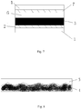
- the device comprises a light absorption layer 3 comprising a semiconductor material 4 and, absorbed thereto, a layer 7 comprising a dye according to invention or a dye comprising the compound of the invention.
- the semiconductor material 4 comprises a porous structure.
- the porous structure is illustrated by the zigzag line in Figure 8 .
- the device of the invention preferably further comprises at least one substrate 1, an electrode 2 and a counter electrode 7, and a charge transport layer 6, said charge transport layer being provided between said counter electrode and said dye layer 5.
- the substrate layer 1 is preferably a transparent substrate layer selected from glass or plastic. Although there are two, a top and a bottom substrate layer 1 shown in Figure 7 , devices with only one, a top or a bottom transparent substrate layer are also encompassed. Generally, the substrate is then on the side of the counter electrode 7.
- Exemplary plastic substrates are polyethylene terephthalate, polyethylene naphthalate (PEN), polycarbonate, polypropylene, polyimide, 3-acetyl cellulose, and polyethersulfone (PES).
- the conductive layer 2 may be provided by of one of Indium tin oxide (ITO), tin oxide fluoride (FTO), ZnO-Ga 2 O 3 , ZnO-Al 2 O 3 , tin-oxide, antimony tin oxide (ATO) and zinc oxide, for example.
- ITO Indium tin oxide
- FTO tin oxide fluoride
- ZnO-Ga 2 O 3 ZnO-Al 2 O 3
- tin-oxide antimony tin oxide
- ATO antimony tin oxide
- zinc oxide for example.
- the device of the present invention comprises a semiconductor layer (4).
- This layer may be constituted by a single layer or by several layers, generally has an overall thickness of up to 100 ⁇ m, for example up to 60 ⁇ m.
- the device of the invention comprises a layer 4 comprising a semiconductor material, wherein said semiconductor layer has a thickness of smaller than 20 ⁇ m.
- the semiconductor layer 4 with a thickness of smaller than 20 microns may also consist of a single layer or comprise two or more separate layers, for example sub-layers.
- the sub-layers are arranged one above the other, each sub-layer being in continuous contact with the respective one or two neighboring sub-layers.
- the semiconductor layer may comprise a base semiconductor layer having a comparatively low porosity and thereon a comparatively high porosity semiconductor layer, wherein the sensitizers will preferably or to a larger extent be absorbed on the semiconductor material in the high porosity sub-layer.
- the different layers may have different porosity, for example they may be prepared from nanoparticles of different size, but preferably the sizes remain in the ranges given further below.
- the thickness of the entire semiconductor layer, including all potential sub-layers, is preferably ⁇ 20 ⁇ m, more preferably ⁇ 17 ⁇ m, even more preferably ⁇ 15 and most preferably ⁇ 13 ⁇ m.
- the semiconductor material layer 4 may comprises a semiconductor material selected from Si, TiO 2 , SnO 2 , ZnO, WO 3 , Nb 2 O 5 , and TiSrO 3 , which all are exemplary semiconductor materials for the purpose of the invention.
- the semiconductor material layer 4 comprises a porous layer made of semiconductor nanoparticles, for example nanoparticles made of the semiconductor materials above.
- the average diameter of the semiconductor nanoparticles preferably lies in the range of 0.5 nm - 2000 nm, preferably 1-1000 nm, more preferably 2-500 nm, most preferably 5-100 nm.
- the dye is provided in the form of a dye layer 5, which comprises dye molecules according to the present invention, in particular dyes comprising a compound as defined by formula (1), and/or dyes as defined by formula (35), for example the exemplary dyes according to formulae (40)-(44).
- the dye molecules are preferably anchored by way of their anchoring group on the surface of the porous nanoparticle layer 4 and form a monomolecular layer thereon.
- the charge transport layer 6 preferably comprises (a) an electrically conductive hole and/or electron transporting material or (b) an electrolyte. If the charges are transported by said electrically conductive hole and/or electron transporting material, electrons and/or holes move by electronic motion, instead of diffusion of charged molecules.
- electrically conductive layers are preferably based on organic compounds, including polymers. Accordingly, layer 6 may be an electron and/or hole conducting material.
- the charge transport layer is an electrolyte, which is preferred, it comprises a redox-couple.
- Preferred examples of redox couples suitable for dye sensitized solar cells are the I-/I 3 - couple or the SeCN-/Se(CN) 3 - redox couple.
- the electrolyte preferably comprises one or more ionic liquids.
- Ionic liquids are generally defined by the fact that they have a melting point of 100°C or lower.
- anions of suitable ionic liquids may be selected from I - , Br - , Cl - , [N(CN) 2 ] - , [N(SO 2 CF 3 ) 2 ] - , [PF 6 ] - , [BF 4 ] - , [NO 3 ] - , [C(CN) 3 ] - , [B(CN) 4 ] - , [CF 3 COO] - , [ClO 4 ] - , [BF 3 CF 3 ] - , [CF 3 SO 3 ] - , [CF 3 F 2 SO 3 ] - , [CH 3 H 2 SO 3 ] - , [(CF 3 SO 2 ) 2 N] - , [(C 2 H 5 SO 2 ) 2 N] -
- Cations of ionic liquids according to the invention may, for example, be selected from compounds having structures as shown below:
- Preferred substituents of the organic cations shown above are disclosed in WO2007/093961 , on pages 5-7. The preferred cations defined on these pages are entirely incorporated herein by reference.
- the most preferred substituents R are independently selected from H and C1-C15 alkyl. Substituents are selected so that indicated positive charge is obtained.
- alkyl, alkenyl or alkynyl referred to in this specification may be linear, branched or cyclic. Linear alkyls, alkenyls and alkynyls are preferred.
- the electrolyte of the device of the invention may comprise two or more ionic liquids.
- the electrolyte is substantially free of a solvent.
- substantially free of a solvent means that there is less than 5vol.% of added solvent, preferably no added solvent.
- the counter electrode 7 is may comprise or consist of Pt, Au, Ni, Cu, Ag, In, Ru, Pd, Rh, Ir, Os, C, conductive polymer or a combination comprising two or more of the aforementioned.
- conductive polymers from which a suitable counter electrode material may be selected are polymers comprising polyaniline, polypyrrole, polythiophene, polybenzene and acetylene.
- the present invention provides a DSC comprising one or two transparent substrate layers 1, a conductive layer 2, a light absorption layer 3, a charge transport layer 6 and counter electrode 7.
- Said conductive layer 2, said light absorption layer 3, said electrolyte layer 6 and said counter electrode 7 are preferably connected in order, for example between two transparent substrate layers 1.
- the said light absorption layer 3 comprises a semiconductor nanoparticle layer 4 and a dye layer 5.
- the said semiconductor nanoparticle layer 4 is preferably connected with the said conductive layer 2 and the said dyes layer 5 is connected with the said charge transport layer 6.
- 2-Hexylfuran was synthesized according to a literature method ( Sheu, J.-H.; Yen, C.-F.; Huang, H.-C.; Hong, Y.-L. V. J. Org. Chem. 1989, 54, 5126 ).
- 2-Hexylfuran (2.20 g, 14.45 mmol) was dissolved in 40 mL of anhydrous THF and cooled to -78 °C. After addition of n- butyllithium (Aldrich) (6.90 mL, 2.5 M in hexane, 17.34 mmol), the solution was stirred under Ar at -78 °C for 1 h.
- n-Butyllithium (6.94 mmol) was slowly added dropwise to a solution of 5-octylthieno[3,2- b ]thiophene (5.94 mmol) in anhydrous THF at ⁇ 78 °C under Ar. The mixture was stirred at this temperature for 30 min and then for 1.5 h at room temperature followed, after cooling to ⁇ 78 °C, by the addition of tributylstannyl chloride (7.52 mmol). After stirring for 4 h at room temperature, the reaction was terminated by adding a saturated NH 4 Cl aqueous solution. The mixture was extracted with CH 2 Cl 2 and dried over MgSO 4 .
- Compound 1a is obtained from Aldrich.
- Compound 1b corresponds to ligand L1 obtained in Example 1 (1.) above.
- the dyes of formulae (41)-(44) were synthesized using corresponding starting materials instead of 1b according to an analogues procedure. For example, by using the octylthieno[3,2-b]thiophen bipyridine ligand (L2) obtained in Example 1 (3.) above, instead of L1 of Example 1, dye (41) of the present invention is obtained.
- a screen-printed double layer film of TiO 2 particles was used as photoanode.
- a 7 ⁇ m thick film of 20 nm sized TiO 2 particles was first printed on the fluorine-doped SnO 2 conducting glass electrode and further coated by a 5 ⁇ m thick second layer of 400 nm sized light scattering anatase particles. Fabrication procedure for nanocrystalline TiO 2 particles and photoanode with nanostructure double layers of TiO 2 has been reported. ( Wang P. et al., Enhance the Performance of Dye-Sensitized Solar Cells by Co-grafting Amphiphilic Sensitizer and Hexadecylmalonic Acid on TiO2 Nanocrystals, J. Phys. Chem. B., 107, 2003, 14336 ).
- the TiO 2 electrodes were immersed into a solution containing 300 ⁇ M of dye (40), and, in another device, dye (41), in tert-butanol and acetonitrile (volume ratio 1:1) for 16 h.
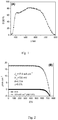
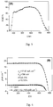
- the dye molecules of the present invention when absorbed on the TiO 2 exhibit a particularly pronounced red-shift, substantially increasing the spectrum of the light absorbed by the light-absorbing surface (here: TiO 2 and absorbed dye). This substantial increase in the red shift could not be expected from the light absorption spectrum of the dyes e in solution.
- dye molecules are particularly densely arranged on the semiconductor surface.
- ⁇ -stacking of the dyes of the invention when absorbed on the surface explains the strong high absorption of light in the red part of the light spectrum and of the dense arrangement of dye molecules.
- the double layered, nanocrystalline TiO 2 film electrode was assembled with a thermally platinized conducting glass electrode.
- the two electrodes were separated by a 35 ⁇ m thick hotmelt ring and sealed up by heating.
- the internal space was filled with an electrolyte consisting of: 1.0 M 1,3-dimethylimidazolium iodide, 0.05 M LiI, 0.1 M guanidinium thiocyanate, 30 mM I 2 , 0.5 M tert -butylpyridine in the mixture of the solvents acetonitrile and valeronitrile (85/15, v/v). After that, the electrolyte-injection hole was sealed.
- an electrolyte consisting of: 1.0 M 1,3-dimethylimidazolium iodide, 0.05 M LiI, 0.1 M guanidinium thiocyanate, 30 mM I 2 , 0.5 M tert -butylpyridine in the mixture of the solvents acetonitrile and valeronitrile (85/15, v/v).
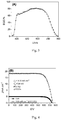
- the short circuit photocurrent density ( J sc ), open circuit photovoltage ( V oc ), and fill factor ( ff ) of the device with dye (20) under AM 1.5 full sunlight (100 mW/cm 2 ) are 17.8 mA cm -2 , 725 mV, and 0.734, respectively, yielding an overall conversion efficiency ( ⁇ ) of 9.5 %.
- Table 1 Photovoltaic device parameters of DSCs According to the Invention dye Open-circuit photovoltage (mV) Short-circuit photocurrent density (mA/cm 2 ) Fill factor ff Conversion efficiency (%) 40 725 17.80 0.734 9.5 41 760 17.87 0.776 10.5 44 728 18.33 0.752 10.0
- the particularly positive results obtained with dye (41) is due to the increased ⁇ -stacking of the dye on the surface of the photoanode, which in is due to the high planarity of the bipyridine antenna ligand substituted with a substituted condensed system of thiophene rings.
- the present invention thus provides ways of increasing the propensity of dye molecules to arrange in an advantageous way on the semiconductor and/or photoelectrode surface.
Landscapes
- Chemical & Material Sciences (AREA)
- Engineering & Computer Science (AREA)
- Organic Chemistry (AREA)
- Power Engineering (AREA)
- Materials Engineering (AREA)
- Crystallography & Structural Chemistry (AREA)
- Inorganic Chemistry (AREA)
- Microelectronics & Electronic Packaging (AREA)
- Chemical Kinetics & Catalysis (AREA)
- Electrochemistry (AREA)
- Hybrid Cells (AREA)
- Photovoltaic Devices (AREA)
Applications Claiming Priority (2)
| Application Number | Priority Date | Filing Date | Title |
|---|---|---|---|
| CN2008100504012A CN101235214B (zh) | 2008-02-27 | 2008-02-27 | 有机钌染料及染料敏化太阳能电池 |
| PCT/IB2009/050800 WO2009107100A2 (en) | 2008-02-27 | 2009-02-27 | High molecular extinction coefficient metal dyes |
Publications (2)
| Publication Number | Publication Date |
|---|---|
| EP2257601A2 EP2257601A2 (en) | 2010-12-08 |
| EP2257601B1 true EP2257601B1 (en) | 2019-04-10 |
Family
ID=39919136
Family Applications (1)
| Application Number | Title | Priority Date | Filing Date |
|---|---|---|---|
| EP09714128.7A Active EP2257601B1 (en) | 2008-02-27 | 2009-02-27 | High molecular extinction coefficient metal dyes |
Country Status (6)
| Country | Link |
|---|---|
| US (1) | US9716240B2 (enExample) |
| EP (1) | EP2257601B1 (enExample) |
| JP (1) | JP5491419B2 (enExample) |
| KR (1) | KR20100132508A (enExample) |
| CN (1) | CN101235214B (enExample) |
| WO (1) | WO2009107100A2 (enExample) |
Families Citing this family (31)
| Publication number | Priority date | Publication date | Assignee | Title |
|---|---|---|---|---|
| EP2351116A1 (en) * | 2008-11-11 | 2011-08-03 | Ecole Polytechnique Fédérale de Lausanne (EPFL) | Novel anchoring ligands for sensitizers of dye-sensitized photovoltaic devices |
| CN101412855B (zh) * | 2008-12-04 | 2011-09-28 | 中国科学院长春应用化学研究所 | 含推S,Se或Te电子基团的联吡啶钌染料及其在染料敏化太阳电池中的应用 |
| KR101050470B1 (ko) * | 2010-04-05 | 2011-07-20 | 삼성에스디아이 주식회사 | 루테늄 착체 및 이를 이용한 염료감응 태양전지 |
| WO2011125024A1 (en) | 2010-04-05 | 2011-10-13 | Ecole Polytechnique Federale De Lausanne (Epfl) | Improved electrode |
| JP5590552B2 (ja) * | 2010-04-13 | 2014-09-17 | 国立大学法人広島大学 | 色素増感型光電変換素子 |
| KR101181262B1 (ko) * | 2010-05-18 | 2012-09-10 | 에스에프씨 주식회사 | 유기염료 및 이를 이용한 염료감응 태양전지 |
| KR101175207B1 (ko) | 2010-05-18 | 2012-08-20 | 에스에프씨 주식회사 | 유기염료 및 이를 이용한 염료감응 태양전지 |
| KR101188803B1 (ko) | 2010-05-20 | 2012-10-09 | (주)씨에스엘쏠라 | 염료 감응 태양 전지용 루테늄계 염료 및 이로부터 제조된 염료 감응 태양 전지 |
| DE102010046412B4 (de) | 2010-09-23 | 2022-01-13 | Merck Patent Gmbh | Metall-Ligand Koordinationsverbindungen |
| DE102010054525A1 (de) | 2010-12-15 | 2012-04-26 | Merck Patent Gmbh | Organische Elektrolumineszenzvorrichtung |
| DE102010055902A1 (de) | 2010-12-23 | 2012-06-28 | Merck Patent Gmbh | Organische Elektrolumineszenzvorrichtung |
| US9923152B2 (en) | 2011-03-24 | 2018-03-20 | Merck Patent Gmbh | Organic ionic functional materials |
| CN102201539A (zh) * | 2011-04-22 | 2011-09-28 | 华北电力大学 | 一种反向结构聚合物太阳电池及其制备方法 |
| KR101323866B1 (ko) * | 2011-04-29 | 2013-10-31 | (주)씨에스엘쏠라 | 신규한 염료 감응 태양 전지용 염료 및 이로부터 제조된 염료 감응 태양 전지 |
| JP6223961B2 (ja) | 2011-05-12 | 2017-11-01 | メルク パテント ゲーエムベーハー | 有機イオン性機能材料、組成物および電子素子 |
| TWI462916B (zh) * | 2011-05-16 | 2014-12-01 | Univ Nat Chiao Tung | 用於染料敏化太陽能電池的釕錯合物光敏染料 |
| DE102012016192A1 (de) | 2011-08-19 | 2013-02-21 | Merck Patent Gmbh | Neue Materialien für organische Elektrolumineszenzvorrichtungen |
| CN102417511B (zh) * | 2011-09-22 | 2013-08-21 | 西北师范大学 | 酰腙锌卟啉及其配合物的合成和应用 |
| WO2013084029A1 (en) | 2011-12-08 | 2013-06-13 | Ecole Polytechnique Federale De Lausanne (Epfl) | Semiconductor electrode comprising a blocking layer |
| WO2014077230A1 (ja) | 2012-11-16 | 2014-05-22 | 田中貴金属工業株式会社 | 使用済み色素溶液からのRu錯体色素の回収方法 |
| JP6407877B2 (ja) | 2012-11-20 | 2018-10-17 | メルク パテント ゲーエムベーハー | 電子素子の製造のための高純度溶媒における調合物 |
| EP2822009A1 (en) | 2013-07-01 | 2015-01-07 | Ecole Polytechnique Fédérale de Lausanne (EPFL) | Solar cell and process for producing the same |
| EP2846371A1 (en) | 2013-09-10 | 2015-03-11 | Ecole Polytechnique Fédérale de Lausanne (EPFL) | Inverted solar cell and process for producing the same |
| CN103554996B (zh) * | 2013-10-11 | 2016-03-02 | 华中科技大学 | 含阳离子的钌络合物染料及其制备的染料敏化太阳能电池 |
| EP2896660A1 (en) | 2014-01-16 | 2015-07-22 | Ecole Polytechnique Federale De Lausanne (Epfl) | Hole transporting and light absorbing material for solid state solar cells |
| EP2903047A1 (en) | 2014-01-31 | 2015-08-05 | Ecole Polytechnique Fédérale de Lausanne (EPFL) | Hole transporting and light absorbing material for solid state solar cells |
| EP2966703A1 (en) | 2014-07-11 | 2016-01-13 | Ecole Polytechnique Fédérale de Lausanne (EPFL) | Template enhanced organic inorganic perovskite heterojunction photovoltaic device |
| US20170301479A1 (en) | 2014-09-10 | 2017-10-19 | Ecole Polytechnique Federale De Lausanne (Epfl) | Photodetector |
| EP3065190A1 (en) | 2015-03-02 | 2016-09-07 | Ecole Polytechnique Fédérale de Lausanne (EPFL) | Small molecule hole transporting material for optoelectronic and photoelectrochemical devices |
| EP3157025A1 (en) | 2015-10-15 | 2017-04-19 | g2e glass2energy SA | Porphyrin-based sensitizer for dye-sensitized solar cell |
| LT6540B (lt) | 2016-09-19 | 2018-06-25 | Kauno technologijos universitetas | Skyles transportuojančios organinės molekulės, turinčios enamino grupių, skirtos optoelektroniniams bei fotoelektroniniams prietaisams |
Family Cites Families (6)
| Publication number | Priority date | Publication date | Assignee | Title |
|---|---|---|---|---|
| FR2895409A1 (fr) | 2005-12-23 | 2007-06-29 | Commissariat Energie Atomique | Complexes sensibilisateurs, leur procede de preparation, materiau hybride inorganique-organique semiconducteur les comprenant, et cellule photovoltaique comprenant ce materiau |
| US8106198B2 (en) * | 2006-02-08 | 2012-01-31 | Shimane Prefectural Government | Photosensitizer dye |
| TWI319424B (en) * | 2006-05-11 | 2010-01-11 | Univ Nat Central | Photosensitizer dye |
| WO2009020098A1 (ja) * | 2007-08-08 | 2009-02-12 | Nippon Kayaku Kabushiki Kaisha | パイ電子共役系を拡張した色素増感型太陽電池用増感色素 |
| EP2053618A1 (en) | 2007-10-25 | 2009-04-29 | Sony Corporation | A dye including an anchoring group in its molecular structure |
| CN101910322A (zh) | 2007-12-26 | 2010-12-08 | 株式会社东进世美肯 | 新型Ru-型敏化剂及其制备方法 |
-
2008
- 2008-02-27 CN CN2008100504012A patent/CN101235214B/zh not_active Expired - Fee Related
-
2009
- 2009-02-27 WO PCT/IB2009/050800 patent/WO2009107100A2/en not_active Ceased
- 2009-02-27 JP JP2010548237A patent/JP5491419B2/ja not_active Expired - Fee Related
- 2009-02-27 US US12/735,942 patent/US9716240B2/en not_active Expired - Fee Related
- 2009-02-27 KR KR1020107021375A patent/KR20100132508A/ko not_active Ceased
- 2009-02-27 EP EP09714128.7A patent/EP2257601B1/en active Active
Non-Patent Citations (1)
| Title |
|---|
| None * |
Also Published As
| Publication number | Publication date |
|---|---|
| JP5491419B2 (ja) | 2014-05-14 |
| JP2011513530A (ja) | 2011-04-28 |
| WO2009107100A2 (en) | 2009-09-03 |
| US20110062541A1 (en) | 2011-03-17 |
| WO2009107100A3 (en) | 2010-04-22 |
| CN101235214A (zh) | 2008-08-06 |
| KR20100132508A (ko) | 2010-12-17 |
| CN101235214B (zh) | 2012-07-04 |
| EP2257601A2 (en) | 2010-12-08 |
| US9716240B2 (en) | 2017-07-25 |
Similar Documents
| Publication | Publication Date | Title |
|---|---|---|
| EP2257601B1 (en) | High molecular extinction coefficient metal dyes | |
| EP2253030B9 (en) | Organic sensitizers | |
| US8445697B2 (en) | Squarylium dyes including an anchoring group | |
| US20090107552A1 (en) | Novel Dyes | |
| CN101570644B (zh) | 以多种杂环及其衍生物作为共轭单元的纯有机染料和由其制备的染料敏化太阳电池 | |
| EP3080206B9 (en) | Porphyrin based sensitizer for dye-sensitized solar cell | |
| KR101472308B1 (ko) | 신규한 루테늄계 염료 및 이의 제조방법 | |
| US9679702B2 (en) | Dye comprising a chromophore to which an acyloin group is attached | |
| Cogal et al. | Asymmetric phthalocyanine derivatives containing 4-carboxyphenyl substituents for dye-sensitized solar cells | |
| CN101429346B (zh) | 以多杂环衍生物作为共轭单元的有机染料和由其制备的染料敏化太阳能电池 | |
| CN101538416B (zh) | 金属有机染料、染料敏化电极、太阳能电池和反应器 | |
| CN101412855B (zh) | 含推S,Se或Te电子基团的联吡啶钌染料及其在染料敏化太阳电池中的应用 | |
| KR100969676B1 (ko) | 신규한 줄로리딘계 염료 및 이의 제조방법 | |
| KR100996236B1 (ko) | 신규한 루테늄계 염료 및 이의 제조방법 | |
| EP2720238A1 (en) | Dye-sensitized solar cells, metal complex dyes therefor, and methods for making such dyes | |
| CN101440222A (zh) | 含硒吩的联吡啶钌染料及其在染料敏化太阳电池中的应用 | |
| Bisht | NIR active squaraine dyes for dye-sensitized solar cells: modulating aggregation, orientation and electronic properties of the dyes |
Legal Events
| Date | Code | Title | Description |
|---|---|---|---|
| PUAI | Public reference made under article 153(3) epc to a published international application that has entered the european phase |
Free format text: ORIGINAL CODE: 0009012 |
|
| 17P | Request for examination filed |
Effective date: 20100924 |
|
| AK | Designated contracting states |
Kind code of ref document: A2 Designated state(s): AT BE BG CH CY CZ DE DK EE ES FI FR GB GR HR HU IE IS IT LI LT LU LV MC MK MT NL NO PL PT RO SE SI SK TR |
|
| AX | Request for extension of the european patent |
Extension state: AL BA RS |
|
| DAX | Request for extension of the european patent (deleted) | ||
| 17Q | First examination report despatched |
Effective date: 20130527 |
|
| STAA | Information on the status of an ep patent application or granted ep patent |
Free format text: STATUS: EXAMINATION IS IN PROGRESS |
|
| GRAP | Despatch of communication of intention to grant a patent |
Free format text: ORIGINAL CODE: EPIDOSNIGR1 |
|
| STAA | Information on the status of an ep patent application or granted ep patent |
Free format text: STATUS: GRANT OF PATENT IS INTENDED |
|
| INTG | Intention to grant announced |
Effective date: 20180725 |
|
| GRAJ | Information related to disapproval of communication of intention to grant by the applicant or resumption of examination proceedings by the epo deleted |
Free format text: ORIGINAL CODE: EPIDOSDIGR1 |
|
| STAA | Information on the status of an ep patent application or granted ep patent |
Free format text: STATUS: EXAMINATION IS IN PROGRESS |
|
| GRAP | Despatch of communication of intention to grant a patent |
Free format text: ORIGINAL CODE: EPIDOSNIGR1 |
|
| STAA | Information on the status of an ep patent application or granted ep patent |
Free format text: STATUS: GRANT OF PATENT IS INTENDED |
|
| INTC | Intention to grant announced (deleted) | ||
| INTG | Intention to grant announced |
Effective date: 20181008 |
|
| RAP1 | Party data changed (applicant data changed or rights of an application transferred) |
Owner name: ECOLE POLYTECHNIQUE FEDERALE DE LAUSANNE (EPFL) |
|
| RIN1 | Information on inventor provided before grant (corrected) |
Inventor name: GAO, FEIFEI Inventor name: GRAETZEL, MICHAEL Inventor name: WANG, YUAN Inventor name: ZAKEERUDDIN, SHAIK, MOHAMMED Inventor name: WANG, PENG Inventor name: ZHANG, JING |
|
| GRAJ | Information related to disapproval of communication of intention to grant by the applicant or resumption of examination proceedings by the epo deleted |
Free format text: ORIGINAL CODE: EPIDOSDIGR1 |
|
| STAA | Information on the status of an ep patent application or granted ep patent |
Free format text: STATUS: EXAMINATION IS IN PROGRESS |
|
| GRAS | Grant fee paid |
Free format text: ORIGINAL CODE: EPIDOSNIGR3 |
|
| STAA | Information on the status of an ep patent application or granted ep patent |
Free format text: STATUS: GRANT OF PATENT IS INTENDED |
|
| INTC | Intention to grant announced (deleted) | ||
| GRAP | Despatch of communication of intention to grant a patent |
Free format text: ORIGINAL CODE: EPIDOSNIGR1 |
|
| GRAA | (expected) grant |
Free format text: ORIGINAL CODE: 0009210 |
|
| STAA | Information on the status of an ep patent application or granted ep patent |
Free format text: STATUS: THE PATENT HAS BEEN GRANTED |
|
| INTG | Intention to grant announced |
Effective date: 20190219 |
|
| AK | Designated contracting states |
Kind code of ref document: B1 Designated state(s): AT BE BG CH CY CZ DE DK EE ES FI FR GB GR HR HU IE IS IT LI LT LU LV MC MK MT NL NO PL PT RO SE SI SK TR |
|
| REG | Reference to a national code |
Ref country code: GB Ref legal event code: FG4D |
|
| REG | Reference to a national code |
Ref country code: CH Ref legal event code: EP Ref country code: AT Ref legal event code: REF Ref document number: 1118591 Country of ref document: AT Kind code of ref document: T Effective date: 20190415 |
|
| REG | Reference to a national code |
Ref country code: DE Ref legal event code: R096 Ref document number: 602009057824 Country of ref document: DE |
|
| REG | Reference to a national code |
Ref country code: IE Ref legal event code: FG4D |
|
| REG | Reference to a national code |
Ref country code: NL Ref legal event code: MP Effective date: 20190410 |
|
| REG | Reference to a national code |
Ref country code: LT Ref legal event code: MG4D |
|
| REG | Reference to a national code |
Ref country code: AT Ref legal event code: MK05 Ref document number: 1118591 Country of ref document: AT Kind code of ref document: T Effective date: 20190410 |
|
| PG25 | Lapsed in a contracting state [announced via postgrant information from national office to epo] |
Ref country code: NL Free format text: LAPSE BECAUSE OF FAILURE TO SUBMIT A TRANSLATION OF THE DESCRIPTION OR TO PAY THE FEE WITHIN THE PRESCRIBED TIME-LIMIT Effective date: 20190410 |
|
| PG25 | Lapsed in a contracting state [announced via postgrant information from national office to epo] |
Ref country code: NO Free format text: LAPSE BECAUSE OF FAILURE TO SUBMIT A TRANSLATION OF THE DESCRIPTION OR TO PAY THE FEE WITHIN THE PRESCRIBED TIME-LIMIT Effective date: 20190710 Ref country code: PT Free format text: LAPSE BECAUSE OF FAILURE TO SUBMIT A TRANSLATION OF THE DESCRIPTION OR TO PAY THE FEE WITHIN THE PRESCRIBED TIME-LIMIT Effective date: 20190910 Ref country code: LT Free format text: LAPSE BECAUSE OF FAILURE TO SUBMIT A TRANSLATION OF THE DESCRIPTION OR TO PAY THE FEE WITHIN THE PRESCRIBED TIME-LIMIT Effective date: 20190410 Ref country code: FI Free format text: LAPSE BECAUSE OF FAILURE TO SUBMIT A TRANSLATION OF THE DESCRIPTION OR TO PAY THE FEE WITHIN THE PRESCRIBED TIME-LIMIT Effective date: 20190410 Ref country code: ES Free format text: LAPSE BECAUSE OF FAILURE TO SUBMIT A TRANSLATION OF THE DESCRIPTION OR TO PAY THE FEE WITHIN THE PRESCRIBED TIME-LIMIT Effective date: 20190410 Ref country code: SE Free format text: LAPSE BECAUSE OF FAILURE TO SUBMIT A TRANSLATION OF THE DESCRIPTION OR TO PAY THE FEE WITHIN THE PRESCRIBED TIME-LIMIT Effective date: 20190410 Ref country code: HR Free format text: LAPSE BECAUSE OF FAILURE TO SUBMIT A TRANSLATION OF THE DESCRIPTION OR TO PAY THE FEE WITHIN THE PRESCRIBED TIME-LIMIT Effective date: 20190410 |
|
| PG25 | Lapsed in a contracting state [announced via postgrant information from national office to epo] |
Ref country code: GR Free format text: LAPSE BECAUSE OF FAILURE TO SUBMIT A TRANSLATION OF THE DESCRIPTION OR TO PAY THE FEE WITHIN THE PRESCRIBED TIME-LIMIT Effective date: 20190711 Ref country code: PL Free format text: LAPSE BECAUSE OF FAILURE TO SUBMIT A TRANSLATION OF THE DESCRIPTION OR TO PAY THE FEE WITHIN THE PRESCRIBED TIME-LIMIT Effective date: 20190410 Ref country code: LV Free format text: LAPSE BECAUSE OF FAILURE TO SUBMIT A TRANSLATION OF THE DESCRIPTION OR TO PAY THE FEE WITHIN THE PRESCRIBED TIME-LIMIT Effective date: 20190410 Ref country code: BG Free format text: LAPSE BECAUSE OF FAILURE TO SUBMIT A TRANSLATION OF THE DESCRIPTION OR TO PAY THE FEE WITHIN THE PRESCRIBED TIME-LIMIT Effective date: 20190710 |
|
| PG25 | Lapsed in a contracting state [announced via postgrant information from national office to epo] |
Ref country code: AT Free format text: LAPSE BECAUSE OF FAILURE TO SUBMIT A TRANSLATION OF THE DESCRIPTION OR TO PAY THE FEE WITHIN THE PRESCRIBED TIME-LIMIT Effective date: 20190410 Ref country code: IS Free format text: LAPSE BECAUSE OF FAILURE TO SUBMIT A TRANSLATION OF THE DESCRIPTION OR TO PAY THE FEE WITHIN THE PRESCRIBED TIME-LIMIT Effective date: 20190810 |
|
| REG | Reference to a national code |
Ref country code: DE Ref legal event code: R097 Ref document number: 602009057824 Country of ref document: DE |
|
| PG25 | Lapsed in a contracting state [announced via postgrant information from national office to epo] |
Ref country code: EE Free format text: LAPSE BECAUSE OF FAILURE TO SUBMIT A TRANSLATION OF THE DESCRIPTION OR TO PAY THE FEE WITHIN THE PRESCRIBED TIME-LIMIT Effective date: 20190410 Ref country code: RO Free format text: LAPSE BECAUSE OF FAILURE TO SUBMIT A TRANSLATION OF THE DESCRIPTION OR TO PAY THE FEE WITHIN THE PRESCRIBED TIME-LIMIT Effective date: 20190410 Ref country code: CZ Free format text: LAPSE BECAUSE OF FAILURE TO SUBMIT A TRANSLATION OF THE DESCRIPTION OR TO PAY THE FEE WITHIN THE PRESCRIBED TIME-LIMIT Effective date: 20190410 Ref country code: DK Free format text: LAPSE BECAUSE OF FAILURE TO SUBMIT A TRANSLATION OF THE DESCRIPTION OR TO PAY THE FEE WITHIN THE PRESCRIBED TIME-LIMIT Effective date: 20190410 Ref country code: SK Free format text: LAPSE BECAUSE OF FAILURE TO SUBMIT A TRANSLATION OF THE DESCRIPTION OR TO PAY THE FEE WITHIN THE PRESCRIBED TIME-LIMIT Effective date: 20190410 |
|
| PLBE | No opposition filed within time limit |
Free format text: ORIGINAL CODE: 0009261 |
|
| STAA | Information on the status of an ep patent application or granted ep patent |
Free format text: STATUS: NO OPPOSITION FILED WITHIN TIME LIMIT |
|
| PG25 | Lapsed in a contracting state [announced via postgrant information from national office to epo] |
Ref country code: IT Free format text: LAPSE BECAUSE OF FAILURE TO SUBMIT A TRANSLATION OF THE DESCRIPTION OR TO PAY THE FEE WITHIN THE PRESCRIBED TIME-LIMIT Effective date: 20190410 |
|
| 26N | No opposition filed |
Effective date: 20200113 |
|
| PG25 | Lapsed in a contracting state [announced via postgrant information from national office to epo] |
Ref country code: TR Free format text: LAPSE BECAUSE OF FAILURE TO SUBMIT A TRANSLATION OF THE DESCRIPTION OR TO PAY THE FEE WITHIN THE PRESCRIBED TIME-LIMIT Effective date: 20190410 |
|
| PG25 | Lapsed in a contracting state [announced via postgrant information from national office to epo] |
Ref country code: SI Free format text: LAPSE BECAUSE OF FAILURE TO SUBMIT A TRANSLATION OF THE DESCRIPTION OR TO PAY THE FEE WITHIN THE PRESCRIBED TIME-LIMIT Effective date: 20190410 |
|
| REG | Reference to a national code |
Ref country code: CH Ref legal event code: PL |
|
| REG | Reference to a national code |
Ref country code: BE Ref legal event code: MM Effective date: 20200229 |
|
| PG25 | Lapsed in a contracting state [announced via postgrant information from national office to epo] |
Ref country code: LU Free format text: LAPSE BECAUSE OF NON-PAYMENT OF DUE FEES Effective date: 20200227 Ref country code: MC Free format text: LAPSE BECAUSE OF FAILURE TO SUBMIT A TRANSLATION OF THE DESCRIPTION OR TO PAY THE FEE WITHIN THE PRESCRIBED TIME-LIMIT Effective date: 20190410 |
|
| PG25 | Lapsed in a contracting state [announced via postgrant information from national office to epo] |
Ref country code: LI Free format text: LAPSE BECAUSE OF NON-PAYMENT OF DUE FEES Effective date: 20200229 Ref country code: CH Free format text: LAPSE BECAUSE OF NON-PAYMENT OF DUE FEES Effective date: 20200229 |
|
| PG25 | Lapsed in a contracting state [announced via postgrant information from national office to epo] |
Ref country code: IE Free format text: LAPSE BECAUSE OF NON-PAYMENT OF DUE FEES Effective date: 20200227 |
|
| PG25 | Lapsed in a contracting state [announced via postgrant information from national office to epo] |
Ref country code: BE Free format text: LAPSE BECAUSE OF NON-PAYMENT OF DUE FEES Effective date: 20200229 |
|
| PGFP | Annual fee paid to national office [announced via postgrant information from national office to epo] |
Ref country code: GB Payment date: 20220223 Year of fee payment: 14 Ref country code: DE Payment date: 20220217 Year of fee payment: 14 |
|
| PG25 | Lapsed in a contracting state [announced via postgrant information from national office to epo] |
Ref country code: MT Free format text: LAPSE BECAUSE OF FAILURE TO SUBMIT A TRANSLATION OF THE DESCRIPTION OR TO PAY THE FEE WITHIN THE PRESCRIBED TIME-LIMIT Effective date: 20190410 Ref country code: CY Free format text: LAPSE BECAUSE OF FAILURE TO SUBMIT A TRANSLATION OF THE DESCRIPTION OR TO PAY THE FEE WITHIN THE PRESCRIBED TIME-LIMIT Effective date: 20190410 |
|
| PGFP | Annual fee paid to national office [announced via postgrant information from national office to epo] |
Ref country code: FR Payment date: 20220216 Year of fee payment: 14 |
|
| PG25 | Lapsed in a contracting state [announced via postgrant information from national office to epo] |
Ref country code: MK Free format text: LAPSE BECAUSE OF FAILURE TO SUBMIT A TRANSLATION OF THE DESCRIPTION OR TO PAY THE FEE WITHIN THE PRESCRIBED TIME-LIMIT Effective date: 20190410 |
|
| REG | Reference to a national code |
Ref country code: DE Ref legal event code: R082 Ref document number: 602009057824 Country of ref document: DE Representative=s name: KARAKATSANIS, GEORGIOS, DR., DE |
|
| REG | Reference to a national code |
Ref country code: DE Ref legal event code: R119 Ref document number: 602009057824 Country of ref document: DE |
|
| GBPC | Gb: european patent ceased through non-payment of renewal fee |
Effective date: 20230227 |
|
| PG25 | Lapsed in a contracting state [announced via postgrant information from national office to epo] |
Ref country code: GB Free format text: LAPSE BECAUSE OF NON-PAYMENT OF DUE FEES Effective date: 20230227 |
|
| PG25 | Lapsed in a contracting state [announced via postgrant information from national office to epo] |
Ref country code: GB Free format text: LAPSE BECAUSE OF NON-PAYMENT OF DUE FEES Effective date: 20230227 Ref country code: FR Free format text: LAPSE BECAUSE OF NON-PAYMENT OF DUE FEES Effective date: 20230228 Ref country code: DE Free format text: LAPSE BECAUSE OF NON-PAYMENT OF DUE FEES Effective date: 20230901 |