EP2257601B1 - High molecular extinction coefficient metal dyes - Google Patents
High molecular extinction coefficient metal dyes Download PDFInfo
- Publication number
- EP2257601B1 EP2257601B1 EP09714128.7A EP09714128A EP2257601B1 EP 2257601 B1 EP2257601 B1 EP 2257601B1 EP 09714128 A EP09714128 A EP 09714128A EP 2257601 B1 EP2257601 B1 EP 2257601B1
- Authority
- EP
- European Patent Office
- Prior art keywords
- dye
- formula
- layer
- compound
- alkyl
- Prior art date
- Legal status (The legal status is an assumption and is not a legal conclusion. Google has not performed a legal analysis and makes no representation as to the accuracy of the status listed.)
- Active
Links
- 229910052751 metal Inorganic materials 0.000 title claims description 10
- 239000002184 metal Substances 0.000 title claims description 10
- 239000000975 dye Substances 0.000 title description 105
- 230000008033 biological extinction Effects 0.000 title description 4
- 150000001875 compounds Chemical class 0.000 claims description 47
- 239000003446 ligand Substances 0.000 claims description 39
- 239000004065 semiconductor Substances 0.000 claims description 35
- 238000006243 chemical reaction Methods 0.000 claims description 29
- 125000001424 substituent group Chemical group 0.000 claims description 27
- 125000000217 alkyl group Chemical group 0.000 claims description 25
- 238000004873 anchoring Methods 0.000 claims description 22
- ROFVEXUMMXZLPA-UHFFFAOYSA-N Bipyridyl Chemical compound N1=CC=CC=C1C1=CC=CC=N1 ROFVEXUMMXZLPA-UHFFFAOYSA-N 0.000 claims description 19
- 229910052736 halogen Inorganic materials 0.000 claims description 19
- 150000002367 halogens Chemical class 0.000 claims description 19
- 239000000463 material Substances 0.000 claims description 19
- 125000003118 aryl group Chemical group 0.000 claims description 18
- 229910052717 sulfur Inorganic materials 0.000 claims description 18
- UFHFLCQGNIYNRP-UHFFFAOYSA-N Hydrogen Chemical compound [H][H] UFHFLCQGNIYNRP-UHFFFAOYSA-N 0.000 claims description 17
- 125000003342 alkenyl group Chemical group 0.000 claims description 17
- 125000000304 alkynyl group Chemical group 0.000 claims description 17
- 229910052739 hydrogen Inorganic materials 0.000 claims description 17
- 239000001257 hydrogen Substances 0.000 claims description 17
- 229910052760 oxygen Inorganic materials 0.000 claims description 17
- 125000003545 alkoxy group Chemical group 0.000 claims description 15
- 150000001350 alkyl halides Chemical class 0.000 claims description 15
- 125000000753 cycloalkyl group Chemical group 0.000 claims description 15
- 230000031700 light absorption Effects 0.000 claims description 11
- 230000001235 sensitizing effect Effects 0.000 claims description 11
- 239000002904 solvent Substances 0.000 claims description 11
- 239000003792 electrolyte Substances 0.000 claims description 10
- 125000002887 hydroxy group Chemical group [H]O* 0.000 claims description 10
- 239000000758 substrate Substances 0.000 claims description 10
- 125000002029 aromatic hydrocarbon group Chemical group 0.000 claims description 9
- 125000004414 alkyl thio group Chemical group 0.000 claims description 8
- 125000003710 aryl alkyl group Chemical group 0.000 claims description 8
- 125000004104 aryloxy group Chemical group 0.000 claims description 8
- 125000004432 carbon atom Chemical group C* 0.000 claims description 8
- 125000003178 carboxy group Chemical group [H]OC(*)=O 0.000 claims description 7
- 125000000623 heterocyclic group Chemical group 0.000 claims description 7
- 239000002608 ionic liquid Substances 0.000 claims description 7
- 150000001335 aliphatic alkanes Chemical class 0.000 claims description 6
- POILWHVDKZOXJZ-ARJAWSKDSA-M (z)-4-oxopent-2-en-2-olate Chemical compound C\C([O-])=C\C(C)=O POILWHVDKZOXJZ-ARJAWSKDSA-M 0.000 claims description 4
- 229910018828 PO3H2 Inorganic materials 0.000 claims description 4
- 125000004429 atom Chemical group 0.000 claims description 3
- 239000010410 layer Substances 0.000 description 62
- GWEVSGVZZGPLCZ-UHFFFAOYSA-N Titan oxide Chemical compound O=[Ti]=O GWEVSGVZZGPLCZ-UHFFFAOYSA-N 0.000 description 25
- 125000005842 heteroatom Chemical group 0.000 description 20
- 239000000203 mixture Substances 0.000 description 11
- YMWUJEATGCHHMB-UHFFFAOYSA-N Dichloromethane Chemical compound ClCCl YMWUJEATGCHHMB-UHFFFAOYSA-N 0.000 description 10
- 150000002902 organometallic compounds Chemical class 0.000 description 10
- 229910052707 ruthenium Inorganic materials 0.000 description 10
- 239000000243 solution Substances 0.000 description 9
- CSNNHWWHGAXBCP-UHFFFAOYSA-L Magnesium sulfate Chemical compound [Mg+2].[O-][S+2]([O-])([O-])[O-] CSNNHWWHGAXBCP-UHFFFAOYSA-L 0.000 description 8
- KJTLSVCANCCWHF-UHFFFAOYSA-N Ruthenium Chemical compound [Ru] KJTLSVCANCCWHF-UHFFFAOYSA-N 0.000 description 8
- HEDRZPFGACZZDS-MICDWDOJSA-N Trichloro(2H)methane Chemical compound [2H]C(Cl)(Cl)Cl HEDRZPFGACZZDS-MICDWDOJSA-N 0.000 description 8
- 238000004519 manufacturing process Methods 0.000 description 8
- 239000002105 nanoparticle Substances 0.000 description 8
- 239000007787 solid Substances 0.000 description 8
- RTZKZFJDLAIYFH-UHFFFAOYSA-N Diethyl ether Chemical compound CCOCC RTZKZFJDLAIYFH-UHFFFAOYSA-N 0.000 description 7
- YTPLMLYBLZKORZ-UHFFFAOYSA-N Thiophene Chemical group C=1C=CSC=1 YTPLMLYBLZKORZ-UHFFFAOYSA-N 0.000 description 7
- 230000015572 biosynthetic process Effects 0.000 description 7
- VLKZOEOYAKHREP-UHFFFAOYSA-N n-Hexane Chemical compound CCCCCC VLKZOEOYAKHREP-UHFFFAOYSA-N 0.000 description 7
- 238000003786 synthesis reaction Methods 0.000 description 7
- WEVYAHXRMPXWCK-UHFFFAOYSA-N Acetonitrile Chemical compound CC#N WEVYAHXRMPXWCK-UHFFFAOYSA-N 0.000 description 6
- 0 CC(*C(C1*C2C1)=C13)=C1OC(*)C(*)OC3=C2[Al]C Chemical compound CC(*C(C1*C2C1)=C13)=C1OC(*)C(*)OC3=C2[Al]C 0.000 description 6
- OKKJLVBELUTLKV-UHFFFAOYSA-N Methanol Chemical compound OC OKKJLVBELUTLKV-UHFFFAOYSA-N 0.000 description 6
- 238000002360 preparation method Methods 0.000 description 6
- 238000001228 spectrum Methods 0.000 description 6
- 238000005160 1H NMR spectroscopy Methods 0.000 description 5
- -1 aminothienyl Chemical group 0.000 description 5
- 239000011521 glass Substances 0.000 description 5
- 238000000034 method Methods 0.000 description 5
- 239000011541 reaction mixture Substances 0.000 description 5
- XOLBLPGZBRYERU-UHFFFAOYSA-N tin dioxide Chemical compound O=[Sn]=O XOLBLPGZBRYERU-UHFFFAOYSA-N 0.000 description 5
- XLYOFNOQVPJJNP-UHFFFAOYSA-N water Substances O XLYOFNOQVPJJNP-UHFFFAOYSA-N 0.000 description 5
- HEDRZPFGACZZDS-UHFFFAOYSA-N Chloroform Chemical compound ClC(Cl)Cl HEDRZPFGACZZDS-UHFFFAOYSA-N 0.000 description 4
- MZRVEZGGRBJDDB-UHFFFAOYSA-N N-Butyllithium Chemical compound [Li]CCCC MZRVEZGGRBJDDB-UHFFFAOYSA-N 0.000 description 4
- VYPSYNLAJGMNEJ-UHFFFAOYSA-N Silicium dioxide Chemical compound O=[Si]=O VYPSYNLAJGMNEJ-UHFFFAOYSA-N 0.000 description 4
- XLOMVQKBTHCTTD-UHFFFAOYSA-N Zinc monoxide Chemical compound [Zn]=O XLOMVQKBTHCTTD-UHFFFAOYSA-N 0.000 description 4
- VSCWAEJMTAWNJL-UHFFFAOYSA-K aluminium trichloride Chemical compound Cl[Al](Cl)Cl VSCWAEJMTAWNJL-UHFFFAOYSA-K 0.000 description 4
- 229910052943 magnesium sulfate Inorganic materials 0.000 description 4
- 239000002245 particle Substances 0.000 description 4
- 239000000741 silica gel Substances 0.000 description 4
- 229910002027 silica gel Inorganic materials 0.000 description 4
- HEMHJVSKTPXQMS-UHFFFAOYSA-M Sodium hydroxide Chemical compound [OH-].[Na+] HEMHJVSKTPXQMS-UHFFFAOYSA-M 0.000 description 3
- 238000001720 action spectrum Methods 0.000 description 3
- 125000002252 acyl group Chemical group 0.000 description 3
- 150000001412 amines Chemical class 0.000 description 3
- 239000007864 aqueous solution Substances 0.000 description 3
- 150000004945 aromatic hydrocarbons Chemical class 0.000 description 3
- 229910052799 carbon Inorganic materials 0.000 description 3
- 238000004440 column chromatography Methods 0.000 description 3
- 125000004122 cyclic group Chemical group 0.000 description 3
- 229910052741 iridium Inorganic materials 0.000 description 3
- 125000001997 phenyl group Chemical group [H]C1=C([H])C([H])=C(*)C([H])=C1[H] 0.000 description 3
- 239000002244 precipitate Substances 0.000 description 3
- 229910052703 rhodium Inorganic materials 0.000 description 3
- 229910052710 silicon Inorganic materials 0.000 description 3
- 239000002356 single layer Substances 0.000 description 3
- 125000000475 sulfinyl group Chemical group [*:2]S([*:1])=O 0.000 description 3
- 125000006732 (C1-C15) alkyl group Chemical group 0.000 description 2
- 125000004169 (C1-C6) alkyl group Chemical group 0.000 description 2
- MOZHJALYAPTCFZ-UHFFFAOYSA-N 1-thieno[3,2-b]thiophen-5-yloctan-1-one Chemical compound S1C=CC2=C1C=C(C(=O)CCCCCCC)S2 MOZHJALYAPTCFZ-UHFFFAOYSA-N 0.000 description 2
- XBLCAKKYMZVLPU-UHFFFAOYSA-N 2-hexylfuran Chemical compound CCCCCCC1=CC=CO1 XBLCAKKYMZVLPU-UHFFFAOYSA-N 0.000 description 2
- QNOZTNXXLYQRPC-UHFFFAOYSA-N 4-(2-octylthieno[3,2-b]thiophen-5-yl)-2-[4-(2-octylthieno[3,2-b]thiophen-5-yl)pyridin-2-yl]pyridine Chemical compound C=1C(C=2SC=3C=C(CCCCCCCC)SC=3C=2)=CC=NC=1C1=CC(C=2SC=3C=C(SC=3C=2)CCCCCCCC)=CC=N1 QNOZTNXXLYQRPC-UHFFFAOYSA-N 0.000 description 2
- GNCHJLGLCHMRCV-UHFFFAOYSA-N 4-(5-hexylfuran-2-yl)-2-[4-(5-hexylfuran-2-yl)pyridin-2-yl]pyridine Chemical compound O1C(CCCCCC)=CC=C1C1=CC=NC(C=2N=CC=C(C=2)C=2OC(CCCCCC)=CC=2)=C1 GNCHJLGLCHMRCV-UHFFFAOYSA-N 0.000 description 2
- KIIHBDSNVJRWFY-UHFFFAOYSA-N 4-bromo-2-(4-bromopyridin-2-yl)pyridine Chemical compound BrC1=CC=NC(C=2N=CC=C(Br)C=2)=C1 KIIHBDSNVJRWFY-UHFFFAOYSA-N 0.000 description 2
- GKCDKORPLHNARQ-UHFFFAOYSA-N 5-octylthieno[3,2-b]thiophene Chemical compound S1C=CC2=C1C=C(CCCCCCCC)S2 GKCDKORPLHNARQ-UHFFFAOYSA-N 0.000 description 2
- NLXLAEXVIDQMFP-UHFFFAOYSA-N Ammonia chloride Chemical compound [NH4+].[Cl-] NLXLAEXVIDQMFP-UHFFFAOYSA-N 0.000 description 2
- IJGRMHOSHXDMSA-UHFFFAOYSA-N Atomic nitrogen Chemical compound N#N IJGRMHOSHXDMSA-UHFFFAOYSA-N 0.000 description 2
- IAZDPXIOMUYVGZ-WFGJKAKNSA-N Dimethyl sulfoxide Chemical compound [2H]C([2H])([2H])S(=O)C([2H])([2H])[2H] IAZDPXIOMUYVGZ-WFGJKAKNSA-N 0.000 description 2
- VEXZGXHMUGYJMC-UHFFFAOYSA-N Hydrochloric acid Chemical compound Cl VEXZGXHMUGYJMC-UHFFFAOYSA-N 0.000 description 2
- JUJWROOIHBZHMG-UHFFFAOYSA-N Pyridine Chemical compound C1=CC=NC=C1 JUJWROOIHBZHMG-UHFFFAOYSA-N 0.000 description 2
- XUIMIQQOPSSXEZ-UHFFFAOYSA-N Silicon Chemical compound [Si] XUIMIQQOPSSXEZ-UHFFFAOYSA-N 0.000 description 2
- NINIDFKCEFEMDL-UHFFFAOYSA-N Sulfur Chemical group [S] NINIDFKCEFEMDL-UHFFFAOYSA-N 0.000 description 2
- DKGAVHZHDRPRBM-UHFFFAOYSA-N Tert-Butanol Chemical compound CC(C)(C)O DKGAVHZHDRPRBM-UHFFFAOYSA-N 0.000 description 2
- GCTFWCDSFPMHHS-UHFFFAOYSA-M Tributyltin chloride Chemical compound CCCC[Sn](Cl)(CCCC)CCCC GCTFWCDSFPMHHS-UHFFFAOYSA-M 0.000 description 2
- 150000001768 cations Chemical class 0.000 description 2
- 229920001940 conductive polymer Polymers 0.000 description 2
- 239000004020 conductor Substances 0.000 description 2
- 239000012043 crude product Substances 0.000 description 2
- XLJMAIOERFSOGZ-UHFFFAOYSA-M cyanate Chemical compound [O-]C#N XLJMAIOERFSOGZ-UHFFFAOYSA-M 0.000 description 2
- 238000002330 electrospray ionisation mass spectrometry Methods 0.000 description 2
- 239000003480 eluent Substances 0.000 description 2
- 230000007613 environmental effect Effects 0.000 description 2
- 239000012948 isocyanate Substances 0.000 description 2
- 150000002513 isocyanates Chemical class 0.000 description 2
- 230000007774 longterm Effects 0.000 description 2
- 125000002496 methyl group Chemical group [H]C([H])([H])* 0.000 description 2
- ZKATWMILCYLAPD-UHFFFAOYSA-N niobium pentoxide Chemical compound O=[Nb](=O)O[Nb](=O)=O ZKATWMILCYLAPD-UHFFFAOYSA-N 0.000 description 2
- 150000002825 nitriles Chemical class 0.000 description 2
- 239000012044 organic layer Substances 0.000 description 2
- 239000004033 plastic Substances 0.000 description 2
- 229920003023 plastic Polymers 0.000 description 2
- 229920000642 polymer Polymers 0.000 description 2
- 229910052702 rhenium Inorganic materials 0.000 description 2
- 239000010703 silicon Substances 0.000 description 2
- 125000006850 spacer group Chemical group 0.000 description 2
- SKRWFPLZQAAQSU-UHFFFAOYSA-N stibanylidynetin;hydrate Chemical compound O.[Sn].[Sb] SKRWFPLZQAAQSU-UHFFFAOYSA-N 0.000 description 2
- 238000003756 stirring Methods 0.000 description 2
- 238000000967 suction filtration Methods 0.000 description 2
- 125000003396 thiol group Chemical group [H]S* 0.000 description 2
- 229910052723 transition metal Inorganic materials 0.000 description 2
- 150000003624 transition metals Chemical class 0.000 description 2
- RIOQSEWOXXDEQQ-UHFFFAOYSA-N triphenylphosphine Chemical compound C1=CC=CC=C1P(C=1C=CC=CC=1)C1=CC=CC=C1 RIOQSEWOXXDEQQ-UHFFFAOYSA-N 0.000 description 2
- 239000011787 zinc oxide Substances 0.000 description 2
- HBENZIXOGRCSQN-VQWWACLZSA-N (1S,2S,6R,14R,15R,16R)-5-(cyclopropylmethyl)-16-[(2S)-2-hydroxy-3,3-dimethylpentan-2-yl]-15-methoxy-13-oxa-5-azahexacyclo[13.2.2.12,8.01,6.02,14.012,20]icosa-8(20),9,11-trien-11-ol Chemical compound N1([C@@H]2CC=3C4=C(C(=CC=3)O)O[C@H]3[C@@]5(OC)CC[C@@]2([C@@]43CC1)C[C@@H]5[C@](C)(O)C(C)(C)CC)CC1CC1 HBENZIXOGRCSQN-VQWWACLZSA-N 0.000 description 1
- 125000000008 (C1-C10) alkyl group Chemical group 0.000 description 1
- 125000003837 (C1-C20) alkyl group Chemical group 0.000 description 1
- KEQXNNJHMWSZHK-UHFFFAOYSA-L 1,3,2,4$l^{2}-dioxathiaplumbetane 2,2-dioxide Chemical compound [Pb+2].[O-]S([O-])(=O)=O KEQXNNJHMWSZHK-UHFFFAOYSA-L 0.000 description 1
- ARSMIBSHEYKMJT-UHFFFAOYSA-M 1,3-dimethylimidazolium iodide Chemical compound [I-].CN1C=C[N+](C)=C1 ARSMIBSHEYKMJT-UHFFFAOYSA-M 0.000 description 1
- WSNDAYQNZRJGMJ-UHFFFAOYSA-N 2,2,2-trifluoroethanone Chemical compound FC(F)(F)[C]=O WSNDAYQNZRJGMJ-UHFFFAOYSA-N 0.000 description 1
- JFJNVIPVOCESGZ-UHFFFAOYSA-N 2,3-dipyridin-2-ylpyridine Chemical compound N1=CC=CC=C1C1=CC=CN=C1C1=CC=CC=N1 JFJNVIPVOCESGZ-UHFFFAOYSA-N 0.000 description 1
- MVDKKZZVTWHVMC-UHFFFAOYSA-N 2-hexadecylpropanedioic acid Chemical compound CCCCCCCCCCCCCCCCC(C(O)=O)C(O)=O MVDKKZZVTWHVMC-UHFFFAOYSA-N 0.000 description 1
- GIFWAJGKWIDXMY-UHFFFAOYSA-N 2-octylthiophene Chemical group CCCCCCCCC1=CC=CS1 GIFWAJGKWIDXMY-UHFFFAOYSA-N 0.000 description 1
- UUIMDJFBHNDZOW-UHFFFAOYSA-N 2-tert-butylpyridine Chemical compound CC(C)(C)C1=CC=CC=N1 UUIMDJFBHNDZOW-UHFFFAOYSA-N 0.000 description 1
- 125000006374 C2-C10 alkenyl group Chemical group 0.000 description 1
- 125000003358 C2-C20 alkenyl group Chemical group 0.000 description 1
- VEXZGXHMUGYJMC-UHFFFAOYSA-M Chloride anion Chemical compound [Cl-] VEXZGXHMUGYJMC-UHFFFAOYSA-M 0.000 description 1
- 229910005143 FSO2 Inorganic materials 0.000 description 1
- KRHYYFGTRYWZRS-UHFFFAOYSA-M Fluoride anion Chemical compound [F-] KRHYYFGTRYWZRS-UHFFFAOYSA-M 0.000 description 1
- 229910010084 LiAlH4 Inorganic materials 0.000 description 1
- 229910014332 N(SO2CF3)2 Inorganic materials 0.000 description 1
- 238000005481 NMR spectroscopy Methods 0.000 description 1
- RFFFKMOABOFIDF-UHFFFAOYSA-N Pentanenitrile Chemical compound CCCCC#N RFFFKMOABOFIDF-UHFFFAOYSA-N 0.000 description 1
- 229920012266 Poly(ether sulfone) PES Polymers 0.000 description 1
- 239000004642 Polyimide Substances 0.000 description 1
- 239000004743 Polypropylene Substances 0.000 description 1
- 229910004074 SiF6 Inorganic materials 0.000 description 1
- 229910008559 TiSrO3 Inorganic materials 0.000 description 1
- 229910007470 ZnO—Al2O3 Inorganic materials 0.000 description 1
- 229910007674 ZnO—Ga2O3 Inorganic materials 0.000 description 1
- ASIIQTABPIPDFG-UHFFFAOYSA-L [Sn+2]=O.[F-].[F-] Chemical compound [Sn+2]=O.[F-].[F-] ASIIQTABPIPDFG-UHFFFAOYSA-L 0.000 description 1
- 238000005299 abrasion Methods 0.000 description 1
- 238000002835 absorbance Methods 0.000 description 1
- 238000010521 absorption reaction Methods 0.000 description 1
- 238000000862 absorption spectrum Methods 0.000 description 1
- 229940081735 acetylcellulose Drugs 0.000 description 1
- 230000002378 acidificating effect Effects 0.000 description 1
- HSFWRNGVRCDJHI-UHFFFAOYSA-N alpha-acetylene Natural products C#C HSFWRNGVRCDJHI-UHFFFAOYSA-N 0.000 description 1
- 150000001450 anions Chemical class 0.000 description 1
- 238000013459 approach Methods 0.000 description 1
- 238000000149 argon plasma sintering Methods 0.000 description 1
- QVGXLLKOCUKJST-UHFFFAOYSA-N atomic oxygen Chemical group [O] QVGXLLKOCUKJST-UHFFFAOYSA-N 0.000 description 1
- 125000002619 bicyclic group Chemical group 0.000 description 1
- 239000003054 catalyst Substances 0.000 description 1
- 230000003197 catalytic effect Effects 0.000 description 1
- 229920002301 cellulose acetate Polymers 0.000 description 1
- 229910001914 chlorine tetroxide Inorganic materials 0.000 description 1
- 230000021615 conjugation Effects 0.000 description 1
- 238000001816 cooling Methods 0.000 description 1
- 229910052802 copper Inorganic materials 0.000 description 1
- 238000005260 corrosion Methods 0.000 description 1
- 230000007797 corrosion Effects 0.000 description 1
- 238000013461 design Methods 0.000 description 1
- 238000009792 diffusion process Methods 0.000 description 1
- 230000000694 effects Effects 0.000 description 1
- 230000005611 electricity Effects 0.000 description 1
- 239000007772 electrode material Substances 0.000 description 1
- 230000005670 electromagnetic radiation Effects 0.000 description 1
- 238000005265 energy consumption Methods 0.000 description 1
- 238000005516 engineering process Methods 0.000 description 1
- 125000005678 ethenylene group Chemical group [H]C([*:1])=C([H])[*:2] 0.000 description 1
- 125000002534 ethynyl group Chemical group [H]C#C* 0.000 description 1
- 239000000706 filtrate Substances 0.000 description 1
- 239000002803 fossil fuel Substances 0.000 description 1
- 229910052732 germanium Inorganic materials 0.000 description 1
- 229910052737 gold Inorganic materials 0.000 description 1
- ZJYYHGLJYGJLLN-UHFFFAOYSA-N guanidinium thiocyanate Chemical compound SC#N.NC(N)=N ZJYYHGLJYGJLLN-UHFFFAOYSA-N 0.000 description 1
- 238000010438 heat treatment Methods 0.000 description 1
- 230000005525 hole transport Effects 0.000 description 1
- 239000012943 hotmelt Substances 0.000 description 1
- 230000006872 improvement Effects 0.000 description 1
- 229910052738 indium Inorganic materials 0.000 description 1
- AMGQUBHHOARCQH-UHFFFAOYSA-N indium;oxotin Chemical compound [In].[Sn]=O AMGQUBHHOARCQH-UHFFFAOYSA-N 0.000 description 1
- 238000002347 injection Methods 0.000 description 1
- 239000007924 injection Substances 0.000 description 1
- 230000003993 interaction Effects 0.000 description 1
- 229910052742 iron Inorganic materials 0.000 description 1
- 229910052745 lead Inorganic materials 0.000 description 1
- 239000007788 liquid Substances 0.000 description 1
- 239000012280 lithium aluminium hydride Substances 0.000 description 1
- 238000002844 melting Methods 0.000 description 1
- 230000008018 melting Effects 0.000 description 1
- SNVLJLYUUXKWOJ-UHFFFAOYSA-N methylidenecarbene Chemical group C=[C] SNVLJLYUUXKWOJ-UHFFFAOYSA-N 0.000 description 1
- GRVDJDISBSALJP-UHFFFAOYSA-N methyloxidanyl Chemical compound [O]C GRVDJDISBSALJP-UHFFFAOYSA-N 0.000 description 1
- 125000002950 monocyclic group Chemical group 0.000 description 1
- GVOISEJVFFIGQE-YCZSINBZSA-N n-[(1r,2s,5r)-5-[methyl(propan-2-yl)amino]-2-[(3s)-2-oxo-3-[[6-(trifluoromethyl)quinazolin-4-yl]amino]pyrrolidin-1-yl]cyclohexyl]acetamide Chemical compound CC(=O)N[C@@H]1C[C@H](N(C)C(C)C)CC[C@@H]1N1C(=O)[C@@H](NC=2C3=CC(=CC=C3N=CN=2)C(F)(F)F)CC1 GVOISEJVFFIGQE-YCZSINBZSA-N 0.000 description 1
- 239000002159 nanocrystal Substances 0.000 description 1
- 239000002086 nanomaterial Substances 0.000 description 1
- 229910052759 nickel Inorganic materials 0.000 description 1
- 229910052757 nitrogen Inorganic materials 0.000 description 1
- 239000012434 nucleophilic reagent Substances 0.000 description 1
- REEZZSHJLXOIHL-UHFFFAOYSA-N octanoyl chloride Chemical compound CCCCCCCC(Cl)=O REEZZSHJLXOIHL-UHFFFAOYSA-N 0.000 description 1
- 150000002892 organic cations Chemical class 0.000 description 1
- 150000002894 organic compounds Chemical class 0.000 description 1
- 125000002524 organometallic group Chemical group 0.000 description 1
- 229910052762 osmium Inorganic materials 0.000 description 1
- 239000001301 oxygen Substances 0.000 description 1
- 125000004430 oxygen atom Chemical group O* 0.000 description 1
- 229910052763 palladium Inorganic materials 0.000 description 1
- QJPQVXSHYBGQGM-UHFFFAOYSA-N palladium;triphenylphosphane Chemical compound [Pd].C1=CC=CC=C1P(C=1C=CC=CC=1)C1=CC=CC=C1.C1=CC=CC=C1P(C=1C=CC=CC=1)C1=CC=CC=C1 QJPQVXSHYBGQGM-UHFFFAOYSA-N 0.000 description 1
- VLTRZXGMWDSKGL-UHFFFAOYSA-M perchlorate Chemical compound [O-]Cl(=O)(=O)=O VLTRZXGMWDSKGL-UHFFFAOYSA-M 0.000 description 1
- 125000000843 phenylene group Chemical group C1(=C(C=CC=C1)*)* 0.000 description 1
- 229910052697 platinum Inorganic materials 0.000 description 1
- 229920000767 polyaniline Polymers 0.000 description 1
- 229920000515 polycarbonate Polymers 0.000 description 1
- 239000004417 polycarbonate Substances 0.000 description 1
- 239000011112 polyethylene naphthalate Substances 0.000 description 1
- 239000005020 polyethylene terephthalate Substances 0.000 description 1
- 229920000139 polyethylene terephthalate Polymers 0.000 description 1
- 229920001721 polyimide Polymers 0.000 description 1
- 229920001155 polypropylene Polymers 0.000 description 1
- 229920000128 polypyrrole Polymers 0.000 description 1
- 229920000123 polythiophene Polymers 0.000 description 1
- UMJSCPRVCHMLSP-UHFFFAOYSA-N pyridine Natural products COC1=CC=CN=C1 UMJSCPRVCHMLSP-UHFFFAOYSA-N 0.000 description 1
- MCJGNVYPOGVAJF-UHFFFAOYSA-N quinolin-8-ol Chemical compound C1=CN=C2C(O)=CC=CC2=C1 MCJGNVYPOGVAJF-UHFFFAOYSA-N 0.000 description 1
- 239000002994 raw material Substances 0.000 description 1
- 230000009467 reduction Effects 0.000 description 1
- 238000010992 reflux Methods 0.000 description 1
- 238000011160 research Methods 0.000 description 1
- 230000027756 respiratory electron transport chain Effects 0.000 description 1
- 230000004044 response Effects 0.000 description 1
- 238000002390 rotary evaporation Methods 0.000 description 1
- YGSDEFSMJLZEOE-UHFFFAOYSA-M salicylate Chemical compound OC1=CC=CC=C1C([O-])=O YGSDEFSMJLZEOE-UHFFFAOYSA-M 0.000 description 1
- 229960001860 salicylate Drugs 0.000 description 1
- 229920006395 saturated elastomer Polymers 0.000 description 1
- 125000001824 selenocyanato group Chemical group *[Se]C#N 0.000 description 1
- 229910052709 silver Inorganic materials 0.000 description 1
- 159000000000 sodium salts Chemical group 0.000 description 1
- 238000001179 sorption measurement Methods 0.000 description 1
- 239000007858 starting material Substances 0.000 description 1
- 239000011593 sulfur Substances 0.000 description 1
- VJYJJHQEVLEOFL-UHFFFAOYSA-N thieno[3,2-b]thiophene Chemical compound S1C=CC2=C1C=CS2 VJYJJHQEVLEOFL-UHFFFAOYSA-N 0.000 description 1
- 125000001544 thienyl group Chemical group 0.000 description 1
- 229930192474 thiophene Natural products 0.000 description 1
- 229910052718 tin Inorganic materials 0.000 description 1
- 229910001887 tin oxide Inorganic materials 0.000 description 1
- 238000004448 titration Methods 0.000 description 1
- 229910000314 transition metal oxide Inorganic materials 0.000 description 1
- OGZAPKLCAUALTI-UHFFFAOYSA-N tributyl-(2-octylthieno[3,2-b]thiophen-5-yl)stannane Chemical compound S1C([Sn](CCCC)(CCCC)CCCC)=CC2=C1C=C(CCCCCCCC)S2 OGZAPKLCAUALTI-UHFFFAOYSA-N 0.000 description 1
- JGMWITPXIMSEKS-UHFFFAOYSA-N tributyl-(5-hexylfuran-2-yl)stannane Chemical compound CCCCCCC1=CC=C([Sn](CCCC)(CCCC)CCCC)O1 JGMWITPXIMSEKS-UHFFFAOYSA-N 0.000 description 1
- ZNOKGRXACCSDPY-UHFFFAOYSA-N tungsten(VI) oxide Inorganic materials O=[W](=O)=O ZNOKGRXACCSDPY-UHFFFAOYSA-N 0.000 description 1
Images
Classifications
-
- H—ELECTRICITY
- H10—SEMICONDUCTOR DEVICES; ELECTRIC SOLID-STATE DEVICES NOT OTHERWISE PROVIDED FOR
- H10K—ORGANIC ELECTRIC SOLID-STATE DEVICES
- H10K85/00—Organic materials used in the body or electrodes of devices covered by this subclass
- H10K85/30—Coordination compounds
- H10K85/341—Transition metal complexes, e.g. Ru(II)polypyridine complexes
- H10K85/344—Transition metal complexes, e.g. Ru(II)polypyridine complexes comprising ruthenium
-
- C—CHEMISTRY; METALLURGY
- C07—ORGANIC CHEMISTRY
- C07F—ACYCLIC, CARBOCYCLIC OR HETEROCYCLIC COMPOUNDS CONTAINING ELEMENTS OTHER THAN CARBON, HYDROGEN, HALOGEN, OXYGEN, NITROGEN, SULFUR, SELENIUM OR TELLURIUM
- C07F15/00—Compounds containing elements of Groups 8, 9, 10 or 18 of the Periodic Table
- C07F15/0006—Compounds containing elements of Groups 8, 9, 10 or 18 of the Periodic Table compounds of the platinum group
- C07F15/0046—Ruthenium compounds
- C07F15/0053—Ruthenium compounds without a metal-carbon linkage
-
- C—CHEMISTRY; METALLURGY
- C09—DYES; PAINTS; POLISHES; NATURAL RESINS; ADHESIVES; COMPOSITIONS NOT OTHERWISE PROVIDED FOR; APPLICATIONS OF MATERIALS NOT OTHERWISE PROVIDED FOR
- C09B—ORGANIC DYES OR CLOSELY-RELATED COMPOUNDS FOR PRODUCING DYES, e.g. PIGMENTS; MORDANTS; LAKES
- C09B57/00—Other synthetic dyes of known constitution
- C09B57/10—Metal complexes of organic compounds not being dyes in uncomplexed form
-
- H—ELECTRICITY
- H01—ELECTRIC ELEMENTS
- H01G—CAPACITORS; CAPACITORS, RECTIFIERS, DETECTORS, SWITCHING DEVICES, LIGHT-SENSITIVE OR TEMPERATURE-SENSITIVE DEVICES OF THE ELECTROLYTIC TYPE
- H01G9/00—Electrolytic capacitors, rectifiers, detectors, switching devices, light-sensitive or temperature-sensitive devices; Processes of their manufacture
- H01G9/20—Light-sensitive devices
- H01G9/2004—Light-sensitive devices characterised by the electrolyte, e.g. comprising an organic electrolyte
- H01G9/2013—Light-sensitive devices characterised by the electrolyte, e.g. comprising an organic electrolyte the electrolyte comprising ionic liquids, e.g. alkyl imidazolium iodide
-
- H—ELECTRICITY
- H01—ELECTRIC ELEMENTS
- H01G—CAPACITORS; CAPACITORS, RECTIFIERS, DETECTORS, SWITCHING DEVICES, LIGHT-SENSITIVE OR TEMPERATURE-SENSITIVE DEVICES OF THE ELECTROLYTIC TYPE
- H01G9/00—Electrolytic capacitors, rectifiers, detectors, switching devices, light-sensitive or temperature-sensitive devices; Processes of their manufacture
- H01G9/20—Light-sensitive devices
- H01G9/2027—Light-sensitive devices comprising an oxide semiconductor electrode
- H01G9/2031—Light-sensitive devices comprising an oxide semiconductor electrode comprising titanium oxide, e.g. TiO2
-
- H—ELECTRICITY
- H01—ELECTRIC ELEMENTS
- H01G—CAPACITORS; CAPACITORS, RECTIFIERS, DETECTORS, SWITCHING DEVICES, LIGHT-SENSITIVE OR TEMPERATURE-SENSITIVE DEVICES OF THE ELECTROLYTIC TYPE
- H01G9/00—Electrolytic capacitors, rectifiers, detectors, switching devices, light-sensitive or temperature-sensitive devices; Processes of their manufacture
- H01G9/20—Light-sensitive devices
- H01G9/2059—Light-sensitive devices comprising an organic dye as the active light absorbing material, e.g. adsorbed on an electrode or dissolved in solution
-
- Y—GENERAL TAGGING OF NEW TECHNOLOGICAL DEVELOPMENTS; GENERAL TAGGING OF CROSS-SECTIONAL TECHNOLOGIES SPANNING OVER SEVERAL SECTIONS OF THE IPC; TECHNICAL SUBJECTS COVERED BY FORMER USPC CROSS-REFERENCE ART COLLECTIONS [XRACs] AND DIGESTS
- Y02—TECHNOLOGIES OR APPLICATIONS FOR MITIGATION OR ADAPTATION AGAINST CLIMATE CHANGE
- Y02E—REDUCTION OF GREENHOUSE GAS [GHG] EMISSIONS, RELATED TO ENERGY GENERATION, TRANSMISSION OR DISTRIBUTION
- Y02E10/00—Energy generation through renewable energy sources
- Y02E10/50—Photovoltaic [PV] energy
- Y02E10/542—Dye sensitized solar cells
-
- Y—GENERAL TAGGING OF NEW TECHNOLOGICAL DEVELOPMENTS; GENERAL TAGGING OF CROSS-SECTIONAL TECHNOLOGIES SPANNING OVER SEVERAL SECTIONS OF THE IPC; TECHNICAL SUBJECTS COVERED BY FORMER USPC CROSS-REFERENCE ART COLLECTIONS [XRACs] AND DIGESTS
- Y02—TECHNOLOGIES OR APPLICATIONS FOR MITIGATION OR ADAPTATION AGAINST CLIMATE CHANGE
- Y02E—REDUCTION OF GREENHOUSE GAS [GHG] EMISSIONS, RELATED TO ENERGY GENERATION, TRANSMISSION OR DISTRIBUTION
- Y02E10/00—Energy generation through renewable energy sources
- Y02E10/50—Photovoltaic [PV] energy
- Y02E10/549—Organic PV cells
Definitions
- the present invention relates to ligands of dyes, in particular of organometallic dyes, that can be used as sensitizers. Furthermore, the present invention relates to the field of photoelectric conversion devices, in particular dye-sensitized solar cells (DSC).
- DSC dye-sensitized solar cells
- DSCs Dye sensitised solar cells
- sensitizers photosensitive dye molecules
- transition metal oxides transition metal oxides
- These properties have given these cells high prospects in the photovoltaic business.
- Prof. Michael Grätzel at the Institutnique Fédérale de Lausanne developed a technological breakthrough in these cells. Since then, DSCs have gradually become a research topic of high interest in the field of solar cells ( Nature 1991, 353, 737 ).
- DSCs used as sensitizers in DSCs are key elements and have a significant impact on stability as well as the device performance, in particular the efficiency.
- DSCs based on bipyridine ruthenium dyes have been developed significantly ( P. Wang, C. Klein, R. Humphry-Baker, S.M. Zakeeruddin and M. Grätzel, J. Am. Chem. Soc., 2004,127, 808 .).
- EP 1985669 A1 ( WO 2007/091525 A1 ) suggests a way to improve the absorbance of the transition metal complex and to impart stability to a nucleophilic reagent to a sensitizer dye.
- the dye improves a bathochromatic effect in absorption.
- This way consists to provide to a divalent transition metal complex comprising a bipyridine ligand substituted by a conjugated system, a vinylene moiety, between the substituent aryl (thienyl or aminothienyl) and the bipyridine ligand.
- WO 2007/071792 A1 discloses sensitizing dyes for solar cells having bipyridine and terpyridine ligands, wherein a poly- or thiophene group is conjugated to one pyridine of the ligand directly or through a spacer. This spacer between the ligand and the poly- or thiophene group is required for improving the electroconversion efficiency of solar cells, namely the efficiency of electron transfer between the sensitizer dye and the solid electrical conductor.
- a dense arrangement of the dye molecules on said surface is expected to increase light absorption and reduce the risk of corrosion and other kind of abrasion of the semiconductor and/or photoelectrode surface.
- a dense arrangement of dye molecules also allows a reduction of the porosity of the surface an also of the overall thickness of the semiconductor layer at the photoanode,
- the present invention addresses the objectives of providing new dyes with low production cost, and high stability, resulting in photovoltaic conversion devices having improved characteristics, such as high energy conversion efficiency.
- the present invention addresses the problems depicted above.
- the present inventors provide novel compounds useful in the preparation of dyes, as well as the dyes comprising these compounds as ligands.
- the dyes obtained according to the invention have high molar extinction coefficients.
- the compounds disclosed are useful in the preparation of sensitizing dyes of DSCs.
- the dyes of the present invention show a particularly pronounced strong red-shift response when absorbed on the photoelectrode surface, typically a TiO 2 surface. In this way more light in the red spectrum of solar light can be utilized for the generation of electricity.
- dye molecules are absorbed in a very densely and tightly, in an ordered arrangement.
- dye molecules are arranged next to each other with aromatic rings of the antenna ligand of the dyes being in a ⁇ -stacked, superimposed relationship. In this way, a particularly dense arrangement is obtained, which further increases light absorption per surface area.
- the inventors believe that the ⁇ -stacking interaction can be positively influenced by using, in the antenna ligand (also known as ancillary ligand) a system of condensed rings, such as condensed thiophene rings.
- the antenna ligand also known as ancillary ligand
- a system of condensed rings such as condensed thiophene rings.
- the planarity of the ligand is increased and a increased stacking can be obtained.
- a dense layer obtained by ⁇ -stacking may also be obtained with antenna ligands based on a bipyridine substituted with chains of aromatic rings comprising and not comprising heteroatoms. Due to the dense stacking of the dye molecules on the photoelectrode and/or semiconductor surface, the thickness of the dye-carrying layer and/or the porosity can be reduced while still maintaining a high light absorption.
- the present invention relates to bipyridine compounds, which are substituted with one or more aromatic hydrocarbons comprising at least one heteroatom.
- the invention provides a use of a compound of formula (1) as a ligand in a metal-containing sensitizing dye, wherein R 1 represents a group which comprises one or more aromatic hydrocarbon moieties selected from the group of the moieties of formulae (4) to (13) or a combination of two or more thereof:
- the invention provides a dye of formula (35) M L 1 L 2 (L 3 ) 2 (35) wherein:
- the present invention provides a photoelectric conversion device comprising a compound of formula (1) wherein R 1 represents a group which comprises one or more aromatic hydrocarbon moieties selected from the group of the moieties of formulae (4) to (13) or a combination of two or more thereof:
- the dyes of the present invention have several advantages. Their production cost is low, they are obtained in high yield and are easy to purify. Furthermore, the molecular design of the dyes of the invention can be easily modified. In particular, the position of R 1 can be easily varied by using the disclosed moieties (2)-(33), preferably (2)-(13), and by selecting any combination comprising two or more of these moieties. More than 85% absorbed light-to-electricity conversion efficiency and higher than 10 % overall cell (energy) conversion efficiency are achieved when the exemplary dyes are used as sensitizers in DSCs. The said dyes have thus a good light-to-electricity conversion performance.
- the present invention relates to bipyridine compounds, which are substituted with one or more aromatic hydrocarbons comprising at least one heteroatom.
- the aromatic hydrocarbon is preferably a further substituted or unsubstituted aryl.
- the heteroatoms provided in said aromatic hydrocarbon are selected from S and O.
- R 1 represents a group which comprises one or more aromatic hydrocarbon moieties selected from the group of moieties of formulae (2) to (33), the moieties of formulae (2), (3) and (14)-(33) not forming part of the invention or a combination of two or more thereof:
- the aryl is preferably an aromatic heterocycle or a system of two, three, four or more fused rings, at least one of which is an aromatic ring comprising at least one heteroatom.
- the moiety R 1 represents the aromatic hydrocarbon, of which the moieties of formulae (4)-(13) represent preferred embodiments, the moieties of formulae (2), (3) and (14) to (33) not forming part of the invention.
- the substituents of the bipyridine compounds of the invention preferably has from 4-50 carbon atoms and 1-30 heteroatoms, more preferably 4-35 carbons and 1-20 heteroatoms, and most preferably 6-25 carbons and 1-10 heteroatoms.
- Preferred heteroatoms are selected from halogen, Se, O and S, more preferably from O and S.
- a and B may be the same (both O or both S) or different (one O and one S).
- a and B are different, meaning that when A is an oxygen atom, B is a sulphur atom and when A is sulfur, B is oxygen.
- substituent R 2 of the compound of formula (1) above it is indicated that said amine, acyl, carboxyl, sulfinyl, alkyl, alkenyl, alkynyl, and aryl may be further substituted.
- Further substituents may be selected from C1-10 alkyl, C2-10 alkenyl, C2-10 alkynyl, which again may be linear, branched or cyclic, and from a mono-or bicyclic C6-C15 aryl.
- further substituent's may also be selected from hydroxyl, sulfhydryl, nitrile, cyanate, and isocyanate. Any alkyl, alkenyl, alkynyl and aryl (also the one of R 2 , not considering the further substituent) may or may not be partially or totally halogenated.
- any alkyl, alkenyl and/or alkynyl mentioned herein is linear or branched.
- Substituents R 2 represent, independently, hydrogen (H), alkyl, alkoxy, cycloalkyl, alkyl halide, halogen, heterocycle, with n ⁇ 0; and, R 3 to R 24 represent, independently, hydrogen (H), hydroxyl, alkyl, cycloalkyl, alkoxy, aryloxy, aralkyl, alkylthio, alkyl halide or halogen.
- the compound of the present invention is selected from a compound of any one of formula (II)-(IV), compounds of formulae (I) and (V)-(VII) not forming part of the invention, below: wherein R 2 is as defined above.
- R 2 comprises from 0-25 carbons and from 0-10 heteroatoms.
- R 2 comprises from 1-15 carbons and from 0-5 heteroatoms, more preferably 1-10 carbons and 0-3 heteroatoms, wherein heteroatoms are defined as above for the moiety - R 1 , -R 2 .
- -R 2 is an alkyl, an alkenyl, an alkynyl or an aryl, in particular an alkyl, an alkenyl, or an alkynyl.
- the present invention provides the use of the compound of the invention as a ligand in an organometallic compound, as a ligand in a dye, as a ligand in a sensitizing compound, and/or as a ligand in a metal-containing sensitizing dye.
- the present invention provides the use of the compounds of the invention as a structural component of a dye and/or as structural a component of an organometallic compound.
- the invention also provides the use of the compounds of the invention as a structural component of a dye of a dye-sensitized photoelectric conversion device.
- the compounds of the invention are useful in the preparation of dyes, organometallic compounds and/or of sensitizers.
- the compounds thus preferably form a structural component of such dyes, organometallic compounds and/or sensitizers, respectively.
- the bipyridine compounds of the invention are used as ligands in dyes, organometallic compounds and/or sensitizers.
- the dyes, organometallic compounds and/or sensitizers comprising the compounds of the invention may, in turn, be used in photoelectric conversion devices. They may in particular be used as sensitizing dyes in such devices, for example.
- the present invention relates to dyes of formula (35): M L 1 L 2 (L 3 ) 2 (35), wherein L 1 is a compound according to the invention.
- the present invention relates to a dye of formula (35): M L 1 L 2 (L 3 ) 2 (35) wherein:
- M is Ru (ruthenium).
- L 2 is an anchoring ligand, which has the purpose of anchoring the dye of formula (35) on a surface of choice.
- the anchoring ligand comprises a structural unit suitable for binding to the metal M and one, two or more anchoring groups. The skilled person will thus select the binding unit and the anchoring group in dependence of the surface to which the overall dye is to be anchored.
- the anchoring ligand L 2 is a bi-pyridine compound of formula (36): wherein R 30 and R 31 are independently one from the other selected fromalkyl, alkenyl, alkynyl, aryl, said alkyl, alkenyl and/or aryl being substituted or unsubstituted, and from anchoring groups which may, for example, be selected from -COOH, -PO 3 H 2 , -PO 4 H 2 , - SO 3 H 2 , SO 4 H 2 , -CONHOH - , acetylacetonate, deprotonated forms of the aforementioned, and chelating anchoring groups with ⁇ -conducting character; with the proviso that at least one of the substituents R 30 and R 31 comprises an anchoring group.
- R 30 and R 31 are independently one from the other selected fromalkyl, alkenyl, alkynyl, aryl, said alkyl, alkenyl and/or aryl being substituted or
- R 30 and R 31 can be an alkyl, alkenyl, alkynyl and/or aryl which is substituted with an anchoring group as cited above, for example.
- L 2 is a bi-pyridine ligand of formula (37) wherein A 1 and A 2 are optional and, if present, are independently selected from an aromatic mono- or bicyclic ring system optionally comprising one or more heteroatoms, and R 32 and R 33 are independently selected from H and from the anchoring groups -COOH, -PO 3 H 2 , - PO 4 H 2 , -SO 3 H 2 , SO 4 H 2 , -CONHOH - , acetylacetonate, deprotonated forms of the aforementioned, and chelating anchoring groups with ⁇ -conducting character; provided that at least one of R 32 and R 33 is an anchoring group.
- a 1 and A 2 may thus be absent, in which case at least one anchoring group, R 32 and/or R 33 , is connected directly to the bipyridine structure of formula (37).
- Examples for the moieties A 1 and A 2 if present, are phenyl and thiophene.
- Examples of chelating anchoring groups with ⁇ -conducting character are oxyme, dioxyme, hydroxyquinoline, salicylate, and ⁇ -keto-enolate groups.
- the present invention provides organometallic compounds selected from the compounds (41)-(43), the compounds (40) and (44) not forming part of the invention, below:
- the present invention relates to the use of dyes and/or organometallic compounds as defined herein as a sensitizer in a dye-sensitized photoelectric conversion device.
- the present invention relates to photoelectric conversion devices.
- the photoelectric conversion device is preferably a photovoltaic cell, in particular a solar cell, capable of converting electromagnetic radiation, in particular visible, infrared and/or UV light, in particular sunlight, into electrical current.
- the photoelectric conversion device is a dye-sensitized conversion device, in particular a dye-sensitized solar cell (DSC).
- DSC dye-sensitized solar cell
- the present invention relates to a photoelectric conversion device comprising a compound, an organometallic compound, a dye, and/or a sensitizer of the invention.
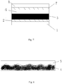
- the device comprises a light absorption layer 3 comprising a semiconductor material 4 and, absorbed thereto, a layer 7 comprising a dye according to invention or a dye comprising the compound of the invention.
- the semiconductor material 4 comprises a porous structure.
- the porous structure is illustrated by the zigzag line in Figure 8 .
- the device of the invention preferably further comprises at least one substrate 1, an electrode 2 and a counter electrode 7, and a charge transport layer 6, said charge transport layer being provided between said counter electrode and said dye layer 5.
- the substrate layer 1 is preferably a transparent substrate layer selected from glass or plastic. Although there are two, a top and a bottom substrate layer 1 shown in Figure 7 , devices with only one, a top or a bottom transparent substrate layer are also encompassed. Generally, the substrate is then on the side of the counter electrode 7.
- Exemplary plastic substrates are polyethylene terephthalate, polyethylene naphthalate (PEN), polycarbonate, polypropylene, polyimide, 3-acetyl cellulose, and polyethersulfone (PES).
- the conductive layer 2 may be provided by of one of Indium tin oxide (ITO), tin oxide fluoride (FTO), ZnO-Ga 2 O 3 , ZnO-Al 2 O 3 , tin-oxide, antimony tin oxide (ATO) and zinc oxide, for example.
- ITO Indium tin oxide
- FTO tin oxide fluoride
- ZnO-Ga 2 O 3 ZnO-Al 2 O 3
- tin-oxide antimony tin oxide
- ATO antimony tin oxide
- zinc oxide for example.
- the device of the present invention comprises a semiconductor layer (4).
- This layer may be constituted by a single layer or by several layers, generally has an overall thickness of up to 100 ⁇ m, for example up to 60 ⁇ m.
- the device of the invention comprises a layer 4 comprising a semiconductor material, wherein said semiconductor layer has a thickness of smaller than 20 ⁇ m.
- the semiconductor layer 4 with a thickness of smaller than 20 microns may also consist of a single layer or comprise two or more separate layers, for example sub-layers.
- the sub-layers are arranged one above the other, each sub-layer being in continuous contact with the respective one or two neighboring sub-layers.
- the semiconductor layer may comprise a base semiconductor layer having a comparatively low porosity and thereon a comparatively high porosity semiconductor layer, wherein the sensitizers will preferably or to a larger extent be absorbed on the semiconductor material in the high porosity sub-layer.
- the different layers may have different porosity, for example they may be prepared from nanoparticles of different size, but preferably the sizes remain in the ranges given further below.
- the thickness of the entire semiconductor layer, including all potential sub-layers, is preferably ⁇ 20 ⁇ m, more preferably ⁇ 17 ⁇ m, even more preferably ⁇ 15 and most preferably ⁇ 13 ⁇ m.
- the semiconductor material layer 4 may comprises a semiconductor material selected from Si, TiO 2 , SnO 2 , ZnO, WO 3 , Nb 2 O 5 , and TiSrO 3 , which all are exemplary semiconductor materials for the purpose of the invention.
- the semiconductor material layer 4 comprises a porous layer made of semiconductor nanoparticles, for example nanoparticles made of the semiconductor materials above.
- the average diameter of the semiconductor nanoparticles preferably lies in the range of 0.5 nm - 2000 nm, preferably 1-1000 nm, more preferably 2-500 nm, most preferably 5-100 nm.
- the dye is provided in the form of a dye layer 5, which comprises dye molecules according to the present invention, in particular dyes comprising a compound as defined by formula (1), and/or dyes as defined by formula (35), for example the exemplary dyes according to formulae (40)-(44).
- the dye molecules are preferably anchored by way of their anchoring group on the surface of the porous nanoparticle layer 4 and form a monomolecular layer thereon.
- the charge transport layer 6 preferably comprises (a) an electrically conductive hole and/or electron transporting material or (b) an electrolyte. If the charges are transported by said electrically conductive hole and/or electron transporting material, electrons and/or holes move by electronic motion, instead of diffusion of charged molecules.
- electrically conductive layers are preferably based on organic compounds, including polymers. Accordingly, layer 6 may be an electron and/or hole conducting material.
- the charge transport layer is an electrolyte, which is preferred, it comprises a redox-couple.
- Preferred examples of redox couples suitable for dye sensitized solar cells are the I-/I 3 - couple or the SeCN-/Se(CN) 3 - redox couple.
- the electrolyte preferably comprises one or more ionic liquids.
- Ionic liquids are generally defined by the fact that they have a melting point of 100°C or lower.
- anions of suitable ionic liquids may be selected from I - , Br - , Cl - , [N(CN) 2 ] - , [N(SO 2 CF 3 ) 2 ] - , [PF 6 ] - , [BF 4 ] - , [NO 3 ] - , [C(CN) 3 ] - , [B(CN) 4 ] - , [CF 3 COO] - , [ClO 4 ] - , [BF 3 CF 3 ] - , [CF 3 SO 3 ] - , [CF 3 F 2 SO 3 ] - , [CH 3 H 2 SO 3 ] - , [(CF 3 SO 2 ) 2 N] - , [(C 2 H 5 SO 2 ) 2 N] -
- Cations of ionic liquids according to the invention may, for example, be selected from compounds having structures as shown below:
- Preferred substituents of the organic cations shown above are disclosed in WO2007/093961 , on pages 5-7. The preferred cations defined on these pages are entirely incorporated herein by reference.
- the most preferred substituents R are independently selected from H and C1-C15 alkyl. Substituents are selected so that indicated positive charge is obtained.
- alkyl, alkenyl or alkynyl referred to in this specification may be linear, branched or cyclic. Linear alkyls, alkenyls and alkynyls are preferred.
- the electrolyte of the device of the invention may comprise two or more ionic liquids.
- the electrolyte is substantially free of a solvent.
- substantially free of a solvent means that there is less than 5vol.% of added solvent, preferably no added solvent.
- the counter electrode 7 is may comprise or consist of Pt, Au, Ni, Cu, Ag, In, Ru, Pd, Rh, Ir, Os, C, conductive polymer or a combination comprising two or more of the aforementioned.
- conductive polymers from which a suitable counter electrode material may be selected are polymers comprising polyaniline, polypyrrole, polythiophene, polybenzene and acetylene.
- the present invention provides a DSC comprising one or two transparent substrate layers 1, a conductive layer 2, a light absorption layer 3, a charge transport layer 6 and counter electrode 7.
- Said conductive layer 2, said light absorption layer 3, said electrolyte layer 6 and said counter electrode 7 are preferably connected in order, for example between two transparent substrate layers 1.
- the said light absorption layer 3 comprises a semiconductor nanoparticle layer 4 and a dye layer 5.
- the said semiconductor nanoparticle layer 4 is preferably connected with the said conductive layer 2 and the said dyes layer 5 is connected with the said charge transport layer 6.
- 2-Hexylfuran was synthesized according to a literature method ( Sheu, J.-H.; Yen, C.-F.; Huang, H.-C.; Hong, Y.-L. V. J. Org. Chem. 1989, 54, 5126 ).
- 2-Hexylfuran (2.20 g, 14.45 mmol) was dissolved in 40 mL of anhydrous THF and cooled to -78 °C. After addition of n- butyllithium (Aldrich) (6.90 mL, 2.5 M in hexane, 17.34 mmol), the solution was stirred under Ar at -78 °C for 1 h.
- n-Butyllithium (6.94 mmol) was slowly added dropwise to a solution of 5-octylthieno[3,2- b ]thiophene (5.94 mmol) in anhydrous THF at ⁇ 78 °C under Ar. The mixture was stirred at this temperature for 30 min and then for 1.5 h at room temperature followed, after cooling to ⁇ 78 °C, by the addition of tributylstannyl chloride (7.52 mmol). After stirring for 4 h at room temperature, the reaction was terminated by adding a saturated NH 4 Cl aqueous solution. The mixture was extracted with CH 2 Cl 2 and dried over MgSO 4 .
- Compound 1a is obtained from Aldrich.
- Compound 1b corresponds to ligand L1 obtained in Example 1 (1.) above.
- the dyes of formulae (41)-(44) were synthesized using corresponding starting materials instead of 1b according to an analogues procedure. For example, by using the octylthieno[3,2-b]thiophen bipyridine ligand (L2) obtained in Example 1 (3.) above, instead of L1 of Example 1, dye (41) of the present invention is obtained.
- a screen-printed double layer film of TiO 2 particles was used as photoanode.
- a 7 ⁇ m thick film of 20 nm sized TiO 2 particles was first printed on the fluorine-doped SnO 2 conducting glass electrode and further coated by a 5 ⁇ m thick second layer of 400 nm sized light scattering anatase particles. Fabrication procedure for nanocrystalline TiO 2 particles and photoanode with nanostructure double layers of TiO 2 has been reported. ( Wang P. et al., Enhance the Performance of Dye-Sensitized Solar Cells by Co-grafting Amphiphilic Sensitizer and Hexadecylmalonic Acid on TiO2 Nanocrystals, J. Phys. Chem. B., 107, 2003, 14336 ).
- the TiO 2 electrodes were immersed into a solution containing 300 ⁇ M of dye (40), and, in another device, dye (41), in tert-butanol and acetonitrile (volume ratio 1:1) for 16 h.
- the dye molecules of the present invention when absorbed on the TiO 2 exhibit a particularly pronounced red-shift, substantially increasing the spectrum of the light absorbed by the light-absorbing surface (here: TiO 2 and absorbed dye). This substantial increase in the red shift could not be expected from the light absorption spectrum of the dyes e in solution.
- dye molecules are particularly densely arranged on the semiconductor surface.
- ⁇ -stacking of the dyes of the invention when absorbed on the surface explains the strong high absorption of light in the red part of the light spectrum and of the dense arrangement of dye molecules.
- the double layered, nanocrystalline TiO 2 film electrode was assembled with a thermally platinized conducting glass electrode.
- the two electrodes were separated by a 35 ⁇ m thick hotmelt ring and sealed up by heating.
- the internal space was filled with an electrolyte consisting of: 1.0 M 1,3-dimethylimidazolium iodide, 0.05 M LiI, 0.1 M guanidinium thiocyanate, 30 mM I 2 , 0.5 M tert -butylpyridine in the mixture of the solvents acetonitrile and valeronitrile (85/15, v/v). After that, the electrolyte-injection hole was sealed.
- an electrolyte consisting of: 1.0 M 1,3-dimethylimidazolium iodide, 0.05 M LiI, 0.1 M guanidinium thiocyanate, 30 mM I 2 , 0.5 M tert -butylpyridine in the mixture of the solvents acetonitrile and valeronitrile (85/15, v/v).
- the short circuit photocurrent density ( J sc ), open circuit photovoltage ( V oc ), and fill factor ( ff ) of the device with dye (20) under AM 1.5 full sunlight (100 mW/cm 2 ) are 17.8 mA cm -2 , 725 mV, and 0.734, respectively, yielding an overall conversion efficiency ( ⁇ ) of 9.5 %.
- Table 1 Photovoltaic device parameters of DSCs According to the Invention dye Open-circuit photovoltage (mV) Short-circuit photocurrent density (mA/cm 2 ) Fill factor ff Conversion efficiency (%) 40 725 17.80 0.734 9.5 41 760 17.87 0.776 10.5 44 728 18.33 0.752 10.0
- the particularly positive results obtained with dye (41) is due to the increased ⁇ -stacking of the dye on the surface of the photoanode, which in is due to the high planarity of the bipyridine antenna ligand substituted with a substituted condensed system of thiophene rings.
- the present invention thus provides ways of increasing the propensity of dye molecules to arrange in an advantageous way on the semiconductor and/or photoelectrode surface.
Landscapes
- Chemical & Material Sciences (AREA)
- Organic Chemistry (AREA)
- Crystallography & Structural Chemistry (AREA)
- Inorganic Chemistry (AREA)
- Engineering & Computer Science (AREA)
- Materials Engineering (AREA)
- Hybrid Cells (AREA)
- Photovoltaic Devices (AREA)
Description
- The present invention relates to ligands of dyes, in particular of organometallic dyes, that can be used as sensitizers. Furthermore, the present invention relates to the field of photoelectric conversion devices, in particular dye-sensitized solar cells (DSC).
- The use of conventional fossil fuels as energy resource poses well-known environmental problems, as well as problems of shortage in the medium to long term. In order to solve the approaching energy crisis, a variety of attempts have been performed. Among the available alternatives, the solar energy, used in photovoltaic cells, is almost unlimited and environment-friendly compared to other forms of energy. The silicon solar cell dominates the photovoltaic business due to the high light-to-electricity conversion efficiency and due to the fact that the technology developed for many decades, is mature. However, silicon solar cells suffer from the disadvantages of a high cost of the production process, expensive raw materials and the difficulty of further increasing the efficiency of the cells.
- Dye sensitised solar cells (DSCs) make use of photosensitive dye molecules (sensitizers) and transition metal oxides, which perform the functions of absorbing visible light, producing electron - hole couples, and transporting the electron produced by light absorption, respectively. DSCs have many advantages, such as high efficiency, low production cost, low energy consumption during manufacturing, and environmental friendly production. These properties have given these cells high prospects in the photovoltaic business. In 1991, Prof. Michael Grätzel at the École Polytechnique Fédérale de Lausanne developed a technological breakthrough in these cells. Since then, DSCs have gradually become a research topic of high interest in the field of solar cells (Nature 1991, 353, 737).
- The dyes used as sensitizers in DSCs are key elements and have a significant impact on stability as well as the device performance, in particular the efficiency. DSCs based on bipyridine ruthenium dyes have been developed significantly (P. Wang, C. Klein, R. Humphry-Baker, S.M. Zakeeruddin and M. Grätzel, J. Am. Chem. Soc., 2004,127, 808.).
-
EP 1985669 A1 (WO 2007/091525 A1 ) suggests a way to improve the absorbance of the transition metal complex and to impart stability to a nucleophilic reagent to a sensitizer dye. The dye improves a bathochromatic effect in absorption. This way consists to provide to a divalent transition metal complex comprising a bipyridine ligand substituted by a conjugated system, a vinylene moiety, between the substituent aryl (thienyl or aminothienyl) and the bipyridine ligand. -
WO 2007/071792 A1 discloses sensitizing dyes for solar cells having bipyridine and terpyridine ligands, wherein a poly- or thiophene group is conjugated to one pyridine of the ligand directly or through a spacer. This spacer between the ligand and the poly- or thiophene group is required for improving the electroconversion efficiency of solar cells, namely the efficiency of electron transfer between the sensitizer dye and the solid electrical conductor. - Chen et al, (Advanced Materials, vol 19, no 22, (2007), pp 3888-3891) suggests that elongating the conjugation length of the anchoring or ancillary ligand (presence of an octyl-thiophene moiety) provides an improvement of the molar extinction coefficient of a metalorganic bipyridine dye.
- In view of the above, it is an objective of the present invention to provide dyes that are useful as sensitizers in DSCs, and which improve device characteristics such as conversion efficiency.
- In particular, it is an objective to provide dyes having high molar extinction coefficients, thus absorbing more light per dye molecule or per molar concentration. In this way, it is hoped to convert more light of the solar spectrum into electrical energy.
- It is an objective of the present invention to prepare dyes that are capable of providing a dense monolayer on the semiconductor and/or photoelectrode surface of a dye-sensitized solar cell. A dense arrangement of the dye molecules on said surface is expected to increase light absorption and reduce the risk of corrosion and other kind of abrasion of the semiconductor and/or photoelectrode surface. In general, it is an objective to increase long term stability of the solar cell. A dense arrangement of dye molecules also allows a reduction of the porosity of the surface an also of the overall thickness of the semiconductor layer at the photoanode,
- Another objective to provide a dye that, when absorbed on a semiconductor is capable of a absorbing as much light of the solar spectrum as possible. In particular, it is an objective to provide dyes that exhibit a pronounced red-shift when absorbed on the photoelectrode and/or semiconductor surface. It is an objective to provide a dye absorbing more photons in the red spectrum of light.
- Generally, it is an objective of the present invention to provide dyes having an increased propensity of arranging and/or being adsorbed on a semiconductor and/or photoelectrode surface of a dye-sensitized solar cell in a manner that positively affects the characteristics of the device, such as conversion efficiency, for example. In other words, it is an objective to judiciously arrange of dye molecules on the photoanode surface by the molecular designing of the structures of such dyes.
- Generally, the present invention addresses the objectives of providing new dyes with low production cost, and high stability, resulting in photovoltaic conversion devices having improved characteristics, such as high energy conversion efficiency.
The present invention addresses the problems depicted above. - The present inventors provide novel compounds useful in the preparation of dyes, as well as the dyes comprising these compounds as ligands. Remarkably, the dyes obtained according to the invention have high molar extinction coefficients. The compounds disclosed are useful in the preparation of sensitizing dyes of DSCs.
- Surprisingly, it is observed that the dyes of the present invention show a particularly pronounced strong red-shift response when absorbed on the photoelectrode surface, typically a TiO2 surface. In this way more light in the red spectrum of solar light can be utilized for the generation of electricity.
- Furthermore, without wishing to be bound by theory, a high degree in stacking is observed with the dyes of the present invention when absorbed on a photoelectrode and/or semiconductor surface. Accordingly, dye molecules are absorbed in a very densely and tightly, in an ordered arrangement. In the ordered arrangement, dye molecules are arranged next to each other with aromatic rings of the antenna ligand of the dyes being in a π-stacked, superimposed relationship. In this way, a particularly dense arrangement is obtained, which further increases light absorption per surface area.
- Without wishing to be bound by theory, the inventors believe that the π-stacking interaction can be positively influenced by using, in the antenna ligand (also known as ancillary ligand) a system of condensed rings, such as condensed thiophene rings. For example, by using a bipyridine ligand substituted with a substituted thieno[3,2-b]thiophenyl, the planarity of the ligand is increased and a increased stacking can be obtained. A dense layer obtained by π-stacking may also be obtained with antenna ligands based on a bipyridine substituted with chains of aromatic rings comprising and not comprising heteroatoms. Due to the dense stacking of the dye molecules on the photoelectrode and/or semiconductor surface, the thickness of the dye-carrying layer and/or the porosity can be reduced while still maintaining a high light absorption.
- Accordingly, the present invention relates to bipyridine compounds, which are substituted with one or more aromatic hydrocarbons comprising at least one heteroatom.
- In one aspect, the invention provides a use of a compound of formula (1)

wherein
R1 represents a group which comprises one or more aromatic hydrocarbon moieties selected from the group of the moieties of formulae (4) to (13) or a combination of two or more thereof:


- wherein n is ≥1;
- wherein A represents O or S; B represents O or S, the said A and B being selected independently one from the other;
- wherein R3 to R24 represent hydrogen (H), hydroxyl, alkyl, cycloalkyl, alkoxy, aryloxy, aralkyl, alkylthio, alkyl halide or halogen; and
- wherein substituents R2 represent hydrogen (H), alkane, alkoxy, cycloalkyl, alkyl- halide, halogen, heterocycle,

- with n ≥ 0.
- In another aspect, the invention provides a dye of formula (35)
M L1 L2 (L3)2 (35)
wherein: - M is the metal atom Ru;
- L1 is a ligand selected from a compound of formula (1)

wherein
R1 represents a group which comprises one or more aromatic hydrocarbon moieties selected from the group of the moieties of formulae (4) to (13) or a combination of two or more thereof:


- wherein n is ≥1;
- wherein A represents O or S; B represents O or S, the said A and B being selected independently one from the other;
- wherein R3 to R24 represent hydrogen (H), hydroxyl, alkyl, cycloalkyl, alkoxy, aryloxy, aralkyl, alkylthio, alkyl halide or halogen; and
- wherein substituents R2 represent hydrogen (H), alkane, alkoxy, cycloalkyl, alkylhalide, halogen, heterocycle,

- L2 is an anchoring ligand of formula (36):

- According to another aspect, the present invention provides a photoelectric conversion device comprising a compound of formula (1)

R1 represents a group which comprises one or more aromatic hydrocarbon moieties selected from the group of the moieties of formulae (4) to (13) or a combination of two or more thereof:


- wherein n is ≥1;
- wherein A represents O or S; B represents O or S, the said A and B being selected independently one from the other;
- wherein R3 to R24 represent hydrogen (H), hydroxyl, alkyl, cycloalkyl, alkoxy,
- aryloxy, aralkyl, alkylthio, alkyl halide or halogen; and
- wherein substituents R2 represent hydrogen (H), alkane, alkoxy, cycloalkyl, alkyl- halide, halogen, heterocycle,

- The dyes of the present invention have several advantages. Their production cost is low, they are obtained in high yield and are easy to purify. Furthermore, the molecular design of the dyes of the invention can be easily modified. In particular, the position of R1 can be easily varied by using the disclosed moieties (2)-(33), preferably (2)-(13), and by selecting any combination comprising two or more of these moieties. More than 85% absorbed light-to-electricity conversion efficiency and higher than 10 % overall cell (energy) conversion efficiency are achieved when the exemplary dyes are used as sensitizers in DSCs. The said dyes have thus a good light-to-electricity conversion performance.
- Further aspects and preferred embodiments of the invention are defined herein below and in the appended claims. Further features and advantages of the invention will become apparent to the skilled person from the description of the preferred embodiments given below.
-
-
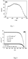
Figure 1 shows the photocurrent action spectrum of a DSC sensitized with the ruthenium dye (40) according to the present invention. -
Figure 2 shows the current density-voltage characteristics of a DSC with the ruthenium dye (40) according to the present invention. -
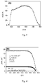
Figure 3 shows the photocurrent action spectrum of a DSC sensitized with the ruthenium dye (41) according to the present invention. -
Figure 4 shows the current density-voltage characteristics of a DSC with the ruthenium dye (41) according to the present invention. -
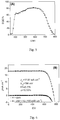
Figure 5 shows the photocurrent action spectrum of a DSC sensitized with the ruthenium dye (44) according to the present invention. -
Figure 6 shows the current density-voltage characteristics of a DSC with the ruthenium dye (44) according to the present invention. -
Figure 7 is a schematic representation of a DSC with a dye according to the present invention. -
Figure 8 is a schematic representation of thelight adsorption layer 3 shown inFigure 7 , comprising a semiconductor nanoparticle layer 4 and adye layer 5. - The present invention relates to bipyridine compounds, which are substituted with one or more aromatic hydrocarbons comprising at least one heteroatom. The aromatic hydrocarbon is preferably a further substituted or unsubstituted aryl. According to an embodiment, the heteroatoms provided in said aromatic hydrocarbon are selected from S and O.
- The present invention relates to compounds of formula (1):

R1 represents a group which comprises one or more aromatic hydrocarbon moieties selected from the group of moieties of formulae (2) to (33), the moieties of formulae (2), (3) and (14)-(33) not forming part of the invention or a combination of two or more thereof:


- wherein, if R1 comprises only the moiety of formula (3) not forming part of the invention, n for moiety of formula (3) is ≥2, and for all other R1 and with all other combinations of moieties formulae (2)-(33), the moieties of formulae (2), (3) and (14)-(33) not forming part of the invention, n is ≥1;
- wherein A represents O or S; B represents O or S, the said A and B being selected independently one from the other, with the proviso that in a compound where R1 is only moiety of formula (2) not forming part of the invention, n is 1 and R2 is alkyl, A is O;
- wherein, in moiety of formula (28) not forming part of the invention, X is selected from any one of C, Si, Ge, Sn or Pb;
- wherein substituents R2 represent, independently, hydrogen (H), halogen, hydroxyl, sulfhydryl, nitrile (-CN), cyanate, isocyanate, amine, acyl, carboxyl, sulfinyl, alkyl, alkenyl, alkynyl, and aryl, wherein said alkyl, alkenyl, alkynyl may be linear, branched or cyclic, and
- wherein said amine, acyl, carboxyl, sulfinyl, alkyl, alkenyl, alkynyl, and aryl may be further substituted, and
- wherein one or more carbon atom, for example one or more methylene carbon atom, in said alkyl, alkenyl, alkynyl, and aryl may be replaced by any heteroatom and/or group selected from the group of -O-, -C(O)-, -C(O)O-, -S-, -S(O)-, SO2-, -S(O)2O-, -N=, -P=,-NR'-, -PR'-, -P(O)(OR')-, -P(O)(OR')O-, -P(O)(NR'R')-, -P(O)(NR'R')O-, P(O)(NR'R')NR'-, -S(O)NR'-, and -S(O)2NR', with R' being H, a C1-C6 alkyl, optionally partially or totally perfluorinated, and/or a phenyl, or a monocyclic aromatic heterocycle, optionally partially or totally perfluorinated;
- wherein Ar is a substituted or unsubstituted ar-diyl devoid of any heteroatom; preferably, Ar comprises from 6 to 25 carbon atoms; preferably, Ar represents a substituted or unsubstituted phenylene;
- wherein R3 to R24 represent, independently, hydrogen (H), hydroxyl, alkyl, alkenyl, alkynyl, aryl, alkoxy, aryloxy, aralkyl, alkylthio, alkyl halide or halogen; and,
- wherein carbon atoms at
positions - The aryl is preferably an aromatic heterocycle or a system of two, three, four or more fused rings, at least one of which is an aromatic ring comprising at least one heteroatom. In the compound of formula (1), the moiety R1 represents the aromatic hydrocarbon, of which the moieties of formulae (4)-(13) represent preferred embodiments, the moieties of formulae (2), (3) and (14) to (33) not forming part of the invention.
- The substituents of the bipyridine compounds of the invention, that is, any entity -R1-R2, preferably has from 4-50 carbon atoms and 1-30 heteroatoms, more preferably 4-35 carbons and 1-20 heteroatoms, and most preferably 6-25 carbons and 1-10 heteroatoms. Preferred heteroatoms are selected from halogen, Se, O and S, more preferably from O and S.
- In a specific moiety of formulae (2)-(33) of the compounds of formula (1) according to the invention, the specific moieties of formulae (2), (3) and (14)-(33) not forming part of the invention, A and B may be the same (both O or both S) or different (one O and one S). Preferably, A and B are different, meaning that when A is an oxygen atom, B is a sulphur atom and when A is sulfur, B is oxygen.
- In a compound of formula (1), not forming part of the invention, where R1 is only moiety of formula (2) and R2 is as defined herein, A is O.
- In the compounds of formula (1) above, in case two moieties carrying substituent's with identical substituent number, for example a compound comprising moieties of formulae (2) and (26) or of formulae (2) and (32), moieties (2), (26) and (32) not forming part of the invention, both carrying a substituent R3 (and also a substituent R4), said identically numbered substituents may be the same or different. For example, on R3 of moiety of formula (2) may be hydrogen and R3 on moiety of formula (26) in the same compound and even in the same R1 may be methyl.
- In the substituent R2 of the compound of formula (1) above, it is indicated that said amine, acyl, carboxyl, sulfinyl, alkyl, alkenyl, alkynyl, and aryl may be further substituted. Further substituents may be selected from C1-10 alkyl, C2-10 alkenyl, C2-10 alkynyl, which again may be linear, branched or cyclic, and from a mono-or bicyclic C6-C15 aryl. At a carbon atom, further substituent's may also be selected from hydroxyl, sulfhydryl, nitrile, cyanate, and isocyanate. Any alkyl, alkenyl, alkynyl and aryl (also the one of R2, not considering the further substituent) may or may not be partially or totally halogenated.
- Preferably, any alkyl, alkenyl and/or alkynyl mentioned herein is linear or branched.
- Substituents R2 represent, independently, hydrogen (H), alkyl, alkoxy, cycloalkyl, alkyl halide, halogen, heterocycle,

R3 to R24 represent, independently, hydrogen (H), hydroxyl, alkyl, cycloalkyl, alkoxy, aryloxy, aralkyl, alkylthio, alkyl halide or halogen. - According to an embodiment, the compound of the present invention is selected from a compound of any one of formula (II)-(IV), compounds of formulae (I) and (V)-(VII) not forming part of the invention, below:


- According to an embodiment of the compounds of the invention, R2 comprises from 0-25 carbons and from 0-10 heteroatoms. Preferably, R2 comprises from 1-15 carbons and from 0-5 heteroatoms, more preferably 1-10 carbons and 0-3 heteroatoms, wherein heteroatoms are defined as above for the moiety - R1, -R2.
- According to a preferred embodiment, -R2 is an alkyl, an alkenyl, an alkynyl or an aryl, in particular an alkyl, an alkenyl, or an alkynyl.
- According to another aspect, the present invention provides the use of the compound of the invention as a ligand in an organometallic compound, as a ligand in a dye, as a ligand in a sensitizing compound, and/or as a ligand in a metal-containing sensitizing dye.
- In further aspects, the present invention provides the use of the compounds of the invention as a structural component of a dye and/or as structural a component of an organometallic compound. The invention also provides the use of the compounds of the invention as a structural component of a dye of a dye-sensitized photoelectric conversion device.
- The compounds of the invention are useful in the preparation of dyes, organometallic compounds and/or of sensitizers. The compounds thus preferably form a structural component of such dyes, organometallic compounds and/or sensitizers, respectively. Preferably, the bipyridine compounds of the invention are used as ligands in dyes, organometallic compounds and/or sensitizers. The dyes, organometallic compounds and/or sensitizers comprising the compounds of the invention may, in turn, be used in photoelectric conversion devices. They may in particular be used as sensitizing dyes in such devices, for example.
- The present invention relates to dyes of formula (35): M L1 L2 (L3)2 (35),
wherein L1 is a compound according to the invention. - The present invention relates to a dye of formula (35):
M L1 L2 (L3)2 (35)
wherein: - M is a metal atom selected from Ru, Os, Ir, Re, Rh, and Fe, Os, Ir, Re, Rh, and Fe not forming part of the invention;
- L1 is a ligand selected from the compounds of formula (1);
- L2 is an anchoring ligand;
- L3 is a spectator ligand.
- According to the invention, M is Ru (ruthenium).
- L2 is an anchoring ligand, which has the purpose of anchoring the dye of formula (35) on a surface of choice. Accordingly, the anchoring ligand comprises a structural unit suitable for binding to the metal M and one, two or more anchoring groups. The skilled person will thus select the binding unit and the anchoring group in dependence of the surface to which the overall dye is to be anchored.
- According to the invention, the anchoring ligand L2 is a bi-pyridine compound of formula (36):

- According to an embodiment, one or both of R30 and R31 can be an alkyl, alkenyl, alkynyl and/or aryl which is substituted with an anchoring group as cited above, for example.
- According to another embodiment, L2 is a bi-pyridine ligand of formula (37)

- Examples of chelating anchoring groups with Π-conducting character are oxyme, dioxyme, hydroxyquinoline, salicylate, and α-keto-enolate groups.
- According to an embodiment, the present invention provides organometallic compounds selected from the compounds (41)-(43), the compounds (40) and (44) not forming part of the invention, below:


- The present invention relates to the use of dyes and/or organometallic compounds as defined herein as a sensitizer in a dye-sensitized photoelectric conversion device.
- The present invention relates to photoelectric conversion devices. The photoelectric conversion device is preferably a photovoltaic cell, in particular a solar cell, capable of converting electromagnetic radiation, in particular visible, infrared and/or UV light, in particular sunlight, into electrical current. According to a preferred embodiment, the photoelectric conversion device is a dye-sensitized conversion device, in particular a dye-sensitized solar cell (DSC). The meanings of the terms "dye", "sensitizer", "sensitising dye" and "dye sensitizer" may partially or totally overlap with each other.
- The present invention relates to a photoelectric conversion device comprising a compound, an organometallic compound, a dye, and/or a sensitizer of the invention.
- For the purpose of illustration, an exemplary, non-limiting embodiment of a DSC according to the invention is shown in
Figures 7 and 8 . The device comprises alight absorption layer 3 comprising a semiconductor material 4 and, absorbed thereto, alayer 7 comprising a dye according to invention or a dye comprising the compound of the invention. - According to a preferred embodiment, the semiconductor material 4 comprises a porous structure. The porous structure is illustrated by the zigzag line in
Figure 8 . - The device of the invention preferably further comprises at least one
substrate 1, anelectrode 2 and acounter electrode 7, and acharge transport layer 6, said charge transport layer being provided between said counter electrode and saiddye layer 5. - The
substrate layer 1 is preferably a transparent substrate layer selected from glass or plastic. Although there are two, a top and abottom substrate layer 1 shown inFigure 7 , devices with only one, a top or a bottom transparent substrate layer are also encompassed. Generally, the substrate is then on the side of thecounter electrode 7. Exemplary plastic substrates are polyethylene terephthalate, polyethylene naphthalate (PEN), polycarbonate, polypropylene, polyimide, 3-acetyl cellulose, and polyethersulfone (PES). - The
conductive layer 2 may be provided by of one of Indium tin oxide (ITO), tin oxide fluoride (FTO), ZnO-Ga2O3, ZnO-Al2O3, tin-oxide, antimony tin oxide (ATO) and zinc oxide, for example. - The device of the present invention comprises a semiconductor layer (4). This layer may be constituted by a single layer or by several layers, generally has an overall thickness of up to 100 µm, for example up to 60 µm. However, according to an embodiment of the present invention, the device of the invention comprises a layer 4 comprising a semiconductor material, wherein said semiconductor layer has a thickness of smaller than 20 µm. The semiconductor layer 4 with a thickness of smaller than 20 microns may also consist of a single layer or comprise two or more separate layers, for example sub-layers. For example, the sub-layers are arranged one above the other, each sub-layer being in continuous contact with the respective one or two neighboring sub-layers. For example, the semiconductor layer may comprise a base semiconductor layer having a comparatively low porosity and thereon a comparatively high porosity semiconductor layer, wherein the sensitizers will preferably or to a larger extent be absorbed on the semiconductor material in the high porosity sub-layer. In other words, the different layers may have different porosity, for example they may be prepared from nanoparticles of different size, but preferably the sizes remain in the ranges given further below. The thickness of the entire semiconductor layer, including all potential sub-layers, is preferably <20 µm, more preferably ≤17 µm, even more preferably ≤15 and most preferably ≤13 µm.
- The semiconductor material layer 4 may comprises a semiconductor material selected from Si, TiO2, SnO2, ZnO, WO3, Nb2O5, and TiSrO3, which all are exemplary semiconductor materials for the purpose of the invention. Preferably, the semiconductor material layer 4 comprises a porous layer made of semiconductor nanoparticles, for example nanoparticles made of the semiconductor materials above. The average diameter of the semiconductor nanoparticles preferably lies in the range of 0.5 nm - 2000 nm, preferably 1-1000 nm, more preferably 2-500 nm, most preferably 5-100 nm.
- The dye is provided in the form of a
dye layer 5, which comprises dye molecules according to the present invention, in particular dyes comprising a compound as defined by formula (1), and/or dyes as defined by formula (35), for example the exemplary dyes according to formulae (40)-(44). The dye molecules are preferably anchored by way of their anchoring group on the surface of the porous nanoparticle layer 4 and form a monomolecular layer thereon. - The
charge transport layer 6 preferably comprises (a) an electrically conductive hole and/or electron transporting material or (b) an electrolyte. If the charges are transported by said electrically conductive hole and/or electron transporting material, electrons and/or holes move by electronic motion, instead of diffusion of charged molecules. Such electrically conductive layers are preferably based on organic compounds, including polymers. Accordingly,layer 6 may be an electron and/or hole conducting material. U. Bach et al. "Solid-state dye-sensitized mesoporous TiO2 solar cells with high photon-to-electron conversion efficiencies", Nature, Vol. 395, October 8, 1998, 583-585, disclose the amorphous organichole transport material WO2007/107961 , charge transporting materials, which are liquid at room temperature and their application in dye-sensitized solar cells are disclosed. These materials may be used, for example, for the purpose of the present invention. - If the charge transport layer is an electrolyte, which is preferred, it comprises a redox-couple. Preferred examples of redox couples suitable for dye sensitized solar cells are the I-/I3- couple or the SeCN-/Se(CN)3- redox couple.
- The electrolyte preferably comprises one or more ionic liquids. Ionic liquids are generally defined by the fact that they have a melting point of 100°C or lower. For example, anions of suitable ionic liquids may be selected from I-, Br-, Cl-, [N(CN)2]-, [N(SO2CF3)2]-, [PF6]-, [BF4]-, [NO3]-, [C(CN)3]-, [B(CN)4]-, [CF3COO]-, [ClO4]-, [BF3CF3]-, [CF3SO3]-, [CF3F2SO3]-, [CH3H2SO3]-, [(CF3SO2)2N]-, [(C2H5SO2)2N]-, [(CF3SO2)3C]-, [(C2F5SO2)3C]-, [(FSO2)3C]-, [CH3CH2OSO3]-, [CF3C(O)O]-, [CF3CF2C(O)O]-, [CH3CH2C(O)O]-, [CH3C(O)O]-, [P(C2H5)3F3]-, [P(CF3)3F3]-, [P(C2H4H)(CF3)2F3]]-, [P(C2F3H2)3F3]-, [P(C2F5)(CF3)2F3]-, [P(CF3)3F3]-, [P(C6H5)3F3]-, [P(C3H7)3F3]-, [P(C4H9)3F3]-, [P(C2H5)2F4]-, [(C2H5)2P(O)O]-, [(C2H5)2P(O)O2]2-, [PC6H5]2F4]-, [(CF3)2P(O)O]-, [(CH3)2P(O)O]-, [(C4H9)2P(O)O]-, [CF3P(O)O2]2-, [CH3P(O)O2]2-, [(CH3O)2P(O)O]-, [BF2(C2F5)2]-, [BF3(C2F5)]-, [BF2(CF3)2]-, [B(C2F5)4]-, [BF3(CN)]-, [BF2(CN)2]-, [B(CF3)4]-, [B(OCH3)4]-, [B(OCH3)2(C2H5)]-, [B(O2C2H4)2]-, [B(O2C2H2)2]-, [B(O2CH4)2]-, [N(CF3)2]-, [AlCl4]- and [SiF6]2-.
- Cations of ionic liquids according to the invention may, for example, be selected from compounds having structures as shown below:


- H, provided that at least one R linked to a heteroatom is different from H;
- a linear or branched C1-C20 alkyl;
- a linear or branched C2-C20 alkenyl, comprising one or several double bonds;
- a linear or branched C2-C20 alkynyl, comprising one or several triple bonds;
- a saturated, partially or totally unsaturated C3-C7 cycloalkyl;
- a halogen, preferably fluoride or chloride, provided that there is no halogen-heteroatom bond;
- NO2, provided that there is no bond of this group with a positively charged heteroatom, and that at least one R is different from NO2;
- CN, provided that there is no bond of this group with a positively charged heteroatom and that at least one R is different from CN;
- wherein the R may be the same or different;
- wherein pairs of R may be connected by single or double bonds;
- wherein one or several R may be partially or totally substituted with halogens, preferably -F and/or -Cl, or partially with -CN or -NO2, provided that not all R are totally halogenated;
- Preferred substituents of the organic cations shown above are disclosed in
WO2007/093961 , on pages 5-7. The preferred cations defined on these pages are entirely incorporated herein by reference. The most preferred substituents R are independently selected from H and C1-C15 alkyl. Substituents are selected so that indicated positive charge is obtained. - Any alkyl, alkenyl or alkynyl referred to in this specification may be linear, branched or cyclic. Linear alkyls, alkenyls and alkynyls are preferred.
- The electrolyte of the device of the invention may comprise two or more ionic liquids. Preferably, the electrolyte is substantially free of a solvent. Substantially free of a solvent means that there is less than 5vol.% of added solvent, preferably no added solvent.
- The
counter electrode 7 is may comprise or consist of Pt, Au, Ni, Cu, Ag, In, Ru, Pd, Rh, Ir, Os, C, conductive polymer or a combination comprising two or more of the aforementioned. Examples of conductive polymers from which a suitable counter electrode material may be selected are polymers comprising polyaniline, polypyrrole, polythiophene, polybenzene and acetylene. - According to a preferred embodiment, the present invention provides a DSC comprising one or two
transparent substrate layers 1, aconductive layer 2, alight absorption layer 3, acharge transport layer 6 andcounter electrode 7. Saidconductive layer 2, saidlight absorption layer 3, saidelectrolyte layer 6 and saidcounter electrode 7 are preferably connected in order, for example between two transparent substrate layers 1. The saidlight absorption layer 3 comprises a semiconductor nanoparticle layer 4 and adye layer 5. The said semiconductor nanoparticle layer 4 is preferably connected with the saidconductive layer 2 and the saiddyes layer 5 is connected with the saidcharge transport layer 6. - The mentioned applications, patents, and publications in the context are listed and incorporated as references in the presented specification. It is supposed that technicians in this field can use the above description within the most extensive scope. Therefore, the optimal embodiment and examples are merely considered as an exemplary illustration and are in no way meant to constitute a restriction in any way.
- The following examples are used for exemplary describing the preparation and synthesis of the compounds, organometallic compounds, dyes and/or sensitizers of the present invention. It does not mean that the scope of the invention is limited to these methods and applications.
- 2-Hexylfuran was synthesized according to a literature method (Sheu, J.-H.; Yen, C.-F.; Huang, H.-C.; Hong, Y.-L. V. J. Org. Chem. 1989, 54, 5126). 2-Hexylfuran (2.20 g, 14.45 mmol) was dissolved in 40 mL of anhydrous THF and cooled to -78 °C. After addition of n-butyllithium (Aldrich) (6.90 mL, 2.5 M in hexane, 17.34 mmol), the solution was stirred under Ar at -78 °C for 1 h. The mixture was stirred for 3 h at 20 °C and then cooled to -78 °C. Tributylstannyl chloride (6.12 g, 18.80 mmol) in 10 mL of anhydrous THF was added dropwise via a syringe and stirred for 2 h at -78 °C. The mixture was stirred overnight at room temperature. The reaction mixture was quenched with aqueous NH4Cl and extracted with CH2Cl2. The combined organic layers were dried over MgSO4. After the removal of solvent, the unpurified 2-hexyl-5-tributylstannylfuran (4.22 g, 9.55 mmol) and 4,4'-dibromo-2,2'-bipyridine (1.00 g, 3.18 mmol) were dissolved in 120 mL of DMF. A catalytic amount of Pd(PPh3)2 Cl2 (0.13 g, 0.16 mmol) was added and the reaction mixture was stirred at 85°C under Ar overnight. After the removal of DMF, the resulting solid was passed through a silica gel column using CHCl3 as eluent to afford L1 (1.12 g, 77% yield) as yellowish solid. 1H NMR (600 MHz, CDCl3, δ H): 8.66 (dd, J) 5.2 Hz, J) 0.6 Hz, 2H), 8.61 (s, 2H), 7.54 (dd, J) 5.2 Hz, J) 1.6 Hz, 2H), 6.93 (d, J) 2.8 Hz, 2H), 6.13 (d, J) 3.2 Hz, 2H), 2.72 (t, J) 7.6 Hz, 4H), 1.75-1.67 (m, 4H), 1.44-1.31 (m, 12H), 0.90 (t, J) 7.0 Hz, 6H). MS (EI) m/z calcd for (C30H36N2O2), 456.62; found, 456.
- To a stirred solution of thieno[3,2-b]thiophene (10.7 mmol) in anhydrous CH2Cl2 (200 mL) was added octanoyl chloride (11.0 mmol). The mixture was stirred for 30 min at room temperature, cooled to 0 °C, and AlCl3 (12.0 mmol) was added portionwise. The mixture was then warmed to 25 °C and stirred overnight. The reaction was quenched by the addition of water and acidified with a 2 M HCl aqueous solution. The mixture was extracted with CH2Cl2. The organic layers were washed with water and dried over MgSO4. After the removal of solvent, the crude product was purified by column chromatography (CH2Cl2/n-hexane: 1/1) on silica gel to afford 1-(thieno[3,2-b]thiophen-2-yl)octan-1-one (2.08 g) as milk white solid. Yield: 72%. 1H NMR (400 MHz, CDCl3, ™H): 7.90 (s, 1H), 7.61 (d, 1H), 7.30 (d, 1H), 2.92 (t, 2H), 1.81↕1.74 (m, 2H), 1.37↕1.30 (m, 8H), 0.88 (t, 3H). Cold anhydrous ether (100 mL) was added to separate batches of LiAlH4 (58.0 mmol) and AlCl3 (13.5 mmol) and the resulting suspended solutions were carefully mixed. To this mixture was added 1-(thieno[3,2-b]thiophen-2-yl)octan-1-one (6.0 mmol) in dry ether at 0 °C. The mixture was warmed to room temperature and then stirred for 3 h. The reaction was quenched by the careful addition of ether and a 2 M HCl aqueous solution. The gray precipitate was filtrated and washed with ether. The combined filtrate was extracted, washed with water, and dried over MgSO4. After rotary evaporation of solvent, the crude product was purified with column chromatography (n-hexane) on silica gel to afford white solid. (1.46 g). Yield: 96%. 1H NMR (400 MHz, CDCl3, ™H): 7.27 (d, 1H), 7.18 (d, 1H), 6.95 (s, 1H), 2.87 (t, 2H), 1.73↕1.53 (m, 2H), 1.39↕1.27 (m, 10H), 0.88 (t, 3H).
- n-Butyllithium (6.94 mmol) was slowly added dropwise to a solution of 5-octylthieno[3,2-b]thiophene (5.94 mmol) in anhydrous THF at ↕78 °C under Ar. The mixture was stirred at this temperature for 30 min and then for 1.5 h at room temperature followed, after cooling to □78 °C, by the addition of tributylstannyl chloride (7.52 mmol). After stirring for 4 h at room temperature, the reaction was terminated by adding a saturated NH4Cl aqueous solution. The mixture was extracted with CH2Cl2 and dried over MgSO4. After the removal of solvent, the crude tributyl(5-octylthieno[3,2-b]thiophen-2-yl)stannane (5.2 mmol) was mixed with 4,4'-dibromo-2,2'-bipyridine (1.72 mmol) in 150 mL DMF. The catalyst Pd(PPh3)2Cl2(0.08 mmol) was added to the solution and the mixture was heated at 85 °C under Ar overnight. After the removal of DMF, the resulting solid was purified by column chromatography on silica gel using CHCl3 as eluent to afford an ivory white solid. Yield: 74%. 1H NMR (400 MHz, CDCl3, ™H): 8.73 (s, 2H), 8.67 (d, 2H), 7.84 (s, 2H), 7.52 (d, 2H), 6.99 (s, 2H), 2.90 (t, 4H), 1.76↕1.72 (m, 4H), 1.41↕1.28 (m, 20H), 0.89 (t, 6H). MS (EI) m/z calcd. for C38H44N2S4: 657.03. Found: 657.24.
-

- The synthetic approach for the preparation of the dyes of the present invention is illustrated by
scheme 1 above, which will be used to describe in more detail the synthesis of dye (40) according to the present invention. - Compound 1a is obtained from Aldrich. Compound 1b corresponds to ligand L1 obtained in Example 1 (1.) above.
- Compounds 1a (0.1 g, 0.16 mmol) and 1b (0.146 g, 0.32 mmol) were dissolved in DMF (50 mL). The reaction mixture was heated to 60°C under nitrogen for 4 hours with constant stirring. To this reaction flask 4,4'-dicarboxylic acid-2,2'-bipyridine (0.08g, 0.32 mmol) was added and refluxed for 4 hours at 140°C. Then an excess of NH4NCS (0.89 g, 13 mmol) was added to the reaction mixture and the reflux was continued for another 4 hours at the same temperature. The reaction mixture was cooled down to room temperature and the solvent (DMF) was removed by using a rotary evaporator under vacuum. Water was added to the flask and the insoluble solid was collected on a sintered glass crucible by suction filtration, washed with water and EtO2, and dried under vacuum. The crude was dissolved in a basic methanol solution (NaOH) and purified by passing through a column. After the collecting main band was concentrated, the pH was lowered to 4.8 by titration with dilute nitric acidic in methanol solution, which produced
dye 20 as a precipitate. The precipitate was collected on a sintered glass crucible by suction filtration and dried in air. The following NMR data for dye 40 (with double sodium salt form) were obtained: 1H NMR (400 MHz, DMSO-d6): δ =0.83(t, 3H), 0.89(t, 3H), 1.26-1.42(m, 12H), 1.62(m, 2H), 1.75(m, 2H), 2.70(t, 2H), 2.83(t, 2H), 6.41(d, 1H), 6.53(d, 1H), 7.28(d, 1H), 7.37(d, 1H), 7.43(d, 1H), 7.61(d, 1H), 7.87(d, 1H), 8.06(d, 1H), 8.32(d, 1H), 8.70(s, 1H), 8.86(s, 1H), 8.94(s, 1H), 9.10 (s, 1H), 9.13(s, 1H), 9.45(d, 1H). - The dyes of formulae (41)-(44) were synthesized using corresponding starting materials instead of 1b according to an analogues procedure. For example, by using the octylthieno[3,2-b]thiophen bipyridine ligand (L2) obtained in Example 1 (3.) above, instead of L1 of Example 1, dye (41) of the present invention is obtained.
- A screen-printed double layer film of TiO2 particles was used as photoanode. A 7 µm thick film of 20 nm sized TiO2 particles was first printed on the fluorine-doped SnO2 conducting glass electrode and further coated by a 5 µm thick second layer of 400 nm sized light scattering anatase particles. Fabrication procedure for nanocrystalline TiO2 particles and photoanode with nanostructure double layers of TiO2 has been reported. (Wang P. et al., Enhance the Performance of Dye-Sensitized Solar Cells by Co-grafting Amphiphilic Sensitizer and Hexadecylmalonic Acid on TiO2 Nanocrystals, J. Phys. Chem. B., 107, 2003, 14336).
- The TiO2 electrodes were immersed into a solution containing 300 µM of dye (40), and, in another device, dye (41), in tert-butanol and acetonitrile (volume ratio 1:1) for 16 h.
- Surprisingly, the dye molecules of the present invention, when absorbed on the TiO2 exhibit a particularly pronounced red-shift, substantially increasing the spectrum of the light absorbed by the light-absorbing surface (here: TiO2 and absorbed dye). This substantial increase in the red shift could not be expected from the light absorption spectrum of the dyes e in solution.
- It is also derived that dye molecules are particularly densely arranged on the semiconductor surface. In conclusion, π -stacking of the dyes of the invention when absorbed on the surface explains the strong high absorption of light in the red part of the light spectrum and of the dense arrangement of dye molecules.
- The double layered, nanocrystalline TiO2 film electrode was assembled with a thermally platinized conducting glass electrode. The two electrodes were separated by a 35µm thick hotmelt ring and sealed up by heating.
- The internal space was filled with an electrolyte consisting of: 1.0
M 1,3-dimethylimidazolium iodide, 0.05 M LiI, 0.1 M guanidinium thiocyanate, 30 mM I2, 0.5 M tert-butylpyridine in the mixture of the solvents acetonitrile and valeronitrile (85/15, v/v). After that, the electrolyte-injection hole was sealed. For the fabrication details see the reference of Wang P. et al., "A Solvent-Free, SeCN-/(SeCN)3- Based Ionic Liquid Electrolyte for High-Efficiency Dye-Sensitized Nanocrystalline Solar Cell", J. Am. Chem. Soc., 126, 2004, 7164. - The short circuit photocurrent density (Jsc ), open circuit photovoltage (Voc ), and fill factor (ff) of the device with dye (20) under AM 1.5 full sunlight (100 mW/cm2) are 17.8 mA cm-2, 725 mV, and 0.734, respectively, yielding an overall conversion efficiency (η) of 9.5 %.
- Further dye-sensitized solar cells were fabricated according to the method of Example 2, and the device characteristics are listed in Table 1 below.
Table 1: Photovoltaic device parameters of DSCs According to the Invention dye Open-circuit photovoltage (mV) Short-circuit photocurrent density (mA/cm2) Fill factor ff Conversion efficiency (%) 40 725 17.80 0.734 9.5 41 760 17.87 0.776 10.5 44 728 18.33 0.752 10.0 - With the other exemplary dyes (42) and (43) of the present invention, devices with similar and performance are obtained.
- Without wishing be bound by theory, it s believed that the particularly positive results obtained with dye (41) is due to the increased π-stacking of the dye on the surface of the photoanode, which in is due to the high planarity of the bipyridine antenna ligand substituted with a substituted condensed system of thiophene rings. The present invention thus provides ways of increasing the propensity of dye molecules to arrange in an advantageous way on the semiconductor and/or photoelectrode surface.
wherein any R is independently selected from H and C1-C15 alkyl.
Claims (15)
- A use of a compound of formula (1)

wherein
R1 represents a group which comprises one or more aromatic hydrocarbon moieties selected from the group of the moieties of formulae (4) to (13) or a combination of two or more thereof:


 wherein n is ≥1;wherein A represents O or S; B represents O or S, the said A and B being selected independently one from the other;wherein R3 to R24 represent hydrogen (H), hydroxyl, alkyl, cycloalkyl, alkoxy, aryloxy, aralkyl, alkylthio, alkyl halide or halogen; andwherein substituents R2 represent hydrogen (H), alkane, alkoxy, cycloalkyl, alkylhalide, halogen, heterocycle,
- The use of claim 1, wherein the compound of formula (1) is selected from a compound according to any one of formula (II)-(IV) below:


- The use according to any one of the preceding claims, wherein the metal-containing sensitizing dye is a dye-sensitizer of a dye-sensitized photoelectric conversion device.
- A dye of formula (35)
M L1 L2 (L3)2 (35)
wherein:M is the metal atom Ru;L1 is a ligand selected from a compound of formula (1)
R1 represents a group which comprises one or more aromatic hydrocarbon moieties selected from the group of the moieties of formulae (4) to (13) or a combination of two or more thereof:


 wherein n is ≥1;wherein A represents O or S; B represents O or S, the said A and B being selected independently one from the other;wherein R3 to R24 represent hydrogen (H), hydroxyl, alkyl, cycloalkyl, alkoxy, aryloxy, aralkyl, alkylthio, alkyl halide or halogen; andwherein substituents R2 represent hydrogen (H), alkane, alkoxy, cycloalkyl, alkylhalide, halogen, heterocycle,
 L2 is an anchoring ligand of formula (36):
 L3 is a spectator ligand.
 - The dye of claim 4, wherein the compound of formula (1) is selected from a compound according to any one of formula (II)-(IV) below:


- The dye of according to any one of claims 4-5, which is selected from any one of compounds (41)-(43) below:


- The dye according to any one of claims 4-6 used as a sensitizer in a dye-sensitized photoelectric conversion device.
- A photoelectric conversion device comprising a compound of formula (1)

R1 represents a group which comprises one or more aromatic hydrocarbon moieties selected from the group of the moieties of formulae (4) to (13) or a combination of two or more thereof:


 wherein n is ≥1;wherein A represents O or S; B represents O or S, the said A and B being selected independently one from the other;wherein R3 to R24 represent hydrogen (H), hydroxyl, alkyl, cycloalkyl, alkoxy, aryloxy, aralkyl, alkylthio, alkyl halide or halogen; andwherein substituents R2 represent hydrogen (H), alkane, alkoxy, cycloalkyl, alkyl- halide, halogen, heterocycle,
 a dye according to any one of claims 4-6.
 - The photoelectric conversion device of claim 8, wherein the compound of formula (1) is selected from a compound according to any one of formula (II)-(IV) below:


- The device according to any one of claims 8-9 comprising a light absorption layer (3) comprising a semiconductor material (4) and, absorbed thereto, a dye layer (5) comprising a dye according to any one of claims 4-6 and/or a dye comprising the compound of formula (1)
- The device according to claim 10, wherein said semiconductor material (4) comprises a layer having a porous structure.
- The device of any one of claims 10-11, further comprising at least one substrate (1), an electrode (2), a counter electrode (7), and a charge transport layer (6), said charge transport layer being provided between said counter electrode (7) and said dye layer (5).
- The device according to claim 12, wherein said charge transport layer comprises (a) an electrically conductive hole and/or electron transporting material or (b) an electrolyte.
- The device according to claim 13, wherein said electrolyte comprises two or more ionic liquids and/or is substantially free of a solvent.
- The device according to any one of claims 10-14, comprising a layer (4) comprising a semiconductor material, said layer (4) optionally being composed of one or more sublayers, wherein said semiconductor layer having a thickness of smaller than 20 µm.
Applications Claiming Priority (2)
| Application Number | Priority Date | Filing Date | Title |
|---|---|---|---|
| CN2008100504012A CN101235214B (en) | 2008-02-27 | 2008-02-27 | Organic ruthenium dye and dye sensitization solar battery |
| PCT/IB2009/050800 WO2009107100A2 (en) | 2008-02-27 | 2009-02-27 | High molecular extinction coefficient metal dyes |
Publications (2)
| Publication Number | Publication Date |
|---|---|
| EP2257601A2 EP2257601A2 (en) | 2010-12-08 |
| EP2257601B1 true EP2257601B1 (en) | 2019-04-10 |
Family
ID=39919136
Family Applications (1)
| Application Number | Title | Priority Date | Filing Date |
|---|---|---|---|
| EP09714128.7A Active EP2257601B1 (en) | 2008-02-27 | 2009-02-27 | High molecular extinction coefficient metal dyes |
Country Status (6)
| Country | Link |
|---|---|
| US (1) | US9716240B2 (en) |
| EP (1) | EP2257601B1 (en) |
| JP (1) | JP5491419B2 (en) |
| KR (1) | KR20100132508A (en) |
| CN (1) | CN101235214B (en) |
| WO (1) | WO2009107100A2 (en) |
Families Citing this family (31)
| Publication number | Priority date | Publication date | Assignee | Title |
|---|---|---|---|---|
| US20110265876A1 (en) * | 2008-11-11 | 2011-11-03 | Universität Ulm | Novel anchoring ligands for sensitizers of dye-sensitized photovoltaic devices |
| CN101412855B (en) * | 2008-12-04 | 2011-09-28 | 中国科学院长春应用化学研究所 | Bipyridine ruthenium dye containing S, Se or Te as donating electron group and use thereof in dye sensitization solar cell |
| WO2011125024A1 (en) | 2010-04-05 | 2011-10-13 | Ecole Polytechnique Federale De Lausanne (Epfl) | Improved electrode |
| KR101050470B1 (en) * | 2010-04-05 | 2011-07-20 | 삼성에스디아이 주식회사 | Ruthenium complex and dye sensitized fuel cell using the same |
| JP5590552B2 (en) * | 2010-04-13 | 2014-09-17 | 国立大学法人広島大学 | Dye-sensitized photoelectric conversion element |
| KR101181262B1 (en) * | 2010-05-18 | 2012-09-10 | 에스에프씨 주식회사 | Organic Dye and Dye-Sensitized Solar Cell |
| KR101175207B1 (en) | 2010-05-18 | 2012-08-20 | 에스에프씨 주식회사 | Organic Dye and Dye-Sensitized Solar Cell |
| KR101188803B1 (en) | 2010-05-20 | 2012-10-09 | (주)씨에스엘쏠라 | NOBLE Ru-TYPE PHOTOSENSITIZER FOR PHOTOVOLTAIC CELL AND PHOTOVOLTAIC CELL PREPARED FROM THE SAME |
| DE102010046412B4 (en) | 2010-09-23 | 2022-01-13 | Merck Patent Gmbh | metal-ligand coordination compounds |
| DE102010054525A1 (en) | 2010-12-15 | 2012-04-26 | Merck Patent Gmbh | Organic electroluminescent device |
| DE102010055902A1 (en) | 2010-12-23 | 2012-06-28 | Merck Patent Gmbh | Organic electroluminescent device |
| WO2012126566A1 (en) | 2011-03-24 | 2012-09-27 | Merck Patent Gmbh | Organic ionic functional materials |
| CN102201539A (en) * | 2011-04-22 | 2011-09-28 | 华北电力大学 | Polymer solar battery with inverted structure and fabrication method thereof |
| KR101323866B1 (en) * | 2011-04-29 | 2013-10-31 | (주)씨에스엘쏠라 | Noble photosensitizer for photovoltaic cell and photovoltaic cell prepared from the same |
| US9496502B2 (en) | 2011-05-12 | 2016-11-15 | Merck Patent Gmbh | Organic ionic compounds, compositions and electronic devices |
| TWI462916B (en) * | 2011-05-16 | 2014-12-01 | Univ Nat Chiao Tung | Ruthenium complex-based photosensitizer dyes for dye-sensitized solar cells |
| DE102012016192A1 (en) | 2011-08-19 | 2013-02-21 | Merck Patent Gmbh | New compounds capable of forming hydrogen bonds are useful in electronic device, e.g. organic electroluminescent device, organic light-emitting transistor and organic light-emitting electrochemical cell |
| CN102417511B (en) * | 2011-09-22 | 2013-08-21 | 西北师范大学 | Acylhydrazone zinc protoporphyrin, and synthesis and application of complex thereof |
| CN104106118B (en) | 2011-12-08 | 2018-06-22 | 洛桑联邦理工学院 | Semi-conducting electrode including barrier layer |
| KR101714288B1 (en) | 2012-11-16 | 2017-03-08 | 다나카 기킨조쿠 고교 가부시키가이샤 | METHOD FOR RECOVERING Ru COMPLEX DYE FROM USED DYE SOLUTION |
| JP6407877B2 (en) | 2012-11-20 | 2018-10-17 | メルク パテント ゲーエムベーハー | Formulations in high purity solvents for the manufacture of electronic devices |
| EP2822009A1 (en) | 2013-07-01 | 2015-01-07 | Ecole Polytechnique Fédérale de Lausanne (EPFL) | Solar cell and process for producing the same |
| EP2846371A1 (en) | 2013-09-10 | 2015-03-11 | Ecole Polytechnique Fédérale de Lausanne (EPFL) | Inverted solar cell and process for producing the same |
| CN103554996B (en) * | 2013-10-11 | 2016-03-02 | 华中科技大学 | The ruthenium complex dye of cation and the dye sensitization solar battery of preparation thereof |
| EP2896660A1 (en) | 2014-01-16 | 2015-07-22 | Ecole Polytechnique Federale De Lausanne (Epfl) | Hole transporting and light absorbing material for solid state solar cells |
| EP2903047A1 (en) | 2014-01-31 | 2015-08-05 | Ecole Polytechnique Fédérale de Lausanne (EPFL) | Hole transporting and light absorbing material for solid state solar cells |
| EP2966703A1 (en) | 2014-07-11 | 2016-01-13 | Ecole Polytechnique Fédérale de Lausanne (EPFL) | Template enhanced organic inorganic perovskite heterojunction photovoltaic device |
| WO2016038501A2 (en) | 2014-09-10 | 2016-03-17 | Ecole Polytechnique Federale De Lausanne (Epfl) | Photodetector |
| EP3065190A1 (en) | 2015-03-02 | 2016-09-07 | Ecole Polytechnique Fédérale de Lausanne (EPFL) | Small molecule hole transporting material for optoelectronic and photoelectrochemical devices |
| EP3157025A1 (en) | 2015-10-15 | 2017-04-19 | g2e glass2energy SA | Porphyrin-based sensitizer for dye-sensitized solar cell |
| LT6540B (en) | 2016-09-19 | 2018-06-25 | Kauno technologijos universitetas | Hole transporting organic molecules containing enamine groups for optoelectronic and photoelectrochemical devices |
Family Cites Families (6)
| Publication number | Priority date | Publication date | Assignee | Title |
|---|---|---|---|---|
| FR2895409A1 (en) * | 2005-12-23 | 2007-06-29 | Commissariat Energie Atomique | SENSITIZING COMPLEXES, PROCESS FOR THE PREPARATION THEREOF, SEMICONDUCTOR INORGANIC-ORGANIC HYBRID MATERIAL COMPRISING SAME, AND PHOTOVOLTAIC CELL COMPRISING THE SAME |
| US8106198B2 (en) * | 2006-02-08 | 2012-01-31 | Shimane Prefectural Government | Photosensitizer dye |
| TWI319424B (en) * | 2006-05-11 | 2010-01-11 | Univ Nat Central | Photosensitizer dye |
| JP5466943B2 (en) * | 2007-08-08 | 2014-04-09 | 日本化薬株式会社 | Sensitizing dye for dye-sensitized solar cell with expanded pi-electron conjugate system |
| EP2053618A1 (en) | 2007-10-25 | 2009-04-29 | Sony Corporation | A dye including an anchoring group in its molecular structure |
| WO2009082163A2 (en) * | 2007-12-26 | 2009-07-02 | Dongjin Semichem Co., Ltd. | Novel ru-type sensitizers and method of preparing the same |
-
2008
- 2008-02-27 CN CN2008100504012A patent/CN101235214B/en not_active Expired - Fee Related
-
2009
- 2009-02-27 EP EP09714128.7A patent/EP2257601B1/en active Active
- 2009-02-27 KR KR1020107021375A patent/KR20100132508A/en not_active Application Discontinuation
- 2009-02-27 US US12/735,942 patent/US9716240B2/en active Active
- 2009-02-27 JP JP2010548237A patent/JP5491419B2/en not_active Expired - Fee Related
- 2009-02-27 WO PCT/IB2009/050800 patent/WO2009107100A2/en active Application Filing
Non-Patent Citations (1)
| Title |
|---|
| None * |
Also Published As
| Publication number | Publication date |
|---|---|
| CN101235214A (en) | 2008-08-06 |
| JP2011513530A (en) | 2011-04-28 |
| CN101235214B (en) | 2012-07-04 |
| US20110062541A1 (en) | 2011-03-17 |
| WO2009107100A2 (en) | 2009-09-03 |
| EP2257601A2 (en) | 2010-12-08 |
| JP5491419B2 (en) | 2014-05-14 |
| KR20100132508A (en) | 2010-12-17 |
| US9716240B2 (en) | 2017-07-25 |
| WO2009107100A3 (en) | 2010-04-22 |
Similar Documents
| Publication | Publication Date | Title |
|---|---|---|
| EP2257601B1 (en) | High molecular extinction coefficient metal dyes | |
| EP2253030B9 (en) | Organic sensitizers | |
| US8445697B2 (en) | Squarylium dyes including an anchoring group | |
| Sun et al. | Viable alternative to N719 for dye-sensitized solar cells | |
| US20090107552A1 (en) | Novel Dyes | |
| EP3080206B1 (en) | Porphyrin based sensitizer for dye-sensitized solar cell | |
| CN101407639A (en) | Organic dye with five-element heterocycle and derivative thereof as conjugate unit, and dye sensitization solar cell prepared thereby | |
| CN101429346B (en) | Organic dye-stuff with multi-heterocycle derivant as conjugation unit and dye sensitized solar battery produced with the same | |
| US9679702B2 (en) | Dye comprising a chromophore to which an acyloin group is attached | |
| Cogal et al. | Asymmetric phthalocyanine derivatives containing 4-carboxyphenyl substituents for dye-sensitized solar cells | |
| KR101472308B1 (en) | A NOBLE Ru-TYPE SENSITIZERS AND METHOD FOR PREPARING OF IT | |
| KR20100136931A (en) | Novel organic dye and preparation thereof | |
| CN101412855B (en) | Bipyridine ruthenium dye containing S, Se or Te as donating electron group and use thereof in dye sensitization solar cell | |
| KR100969676B1 (en) | Novel julolidine-based dye and preparation thereof | |
| KR101173248B1 (en) | Ruthenium dye for dye sensitized solar cell | |
| KR100996236B1 (en) | A NOBLE Ru-TYPE SENSITIZERS AND METHOD FOR PREPARING OF IT | |
| CN101497745A (en) | Organic dye and dye sensitization solar cell prepared thereby | |
| EP2720238A1 (en) | Dye-sensitized solar cells, metal complex dyes therefor, and methods for making such dyes | |
| KR20120046071A (en) | A noble ru-type sensitizers and method for preparing of it |
Legal Events
| Date | Code | Title | Description |
|---|---|---|---|
| PUAI | Public reference made under article 153(3) epc to a published international application that has entered the european phase |
Free format text: ORIGINAL CODE: 0009012 |
|
| 17P | Request for examination filed |
Effective date: 20100924 |
|
| AK | Designated contracting states |
Kind code of ref document: A2 Designated state(s): AT BE BG CH CY CZ DE DK EE ES FI FR GB GR HR HU IE IS IT LI LT LU LV MC MK MT NL NO PL PT RO SE SI SK TR |
|
| AX | Request for extension of the european patent |
Extension state: AL BA RS |
|
| DAX | Request for extension of the european patent (deleted) | ||
| 17Q | First examination report despatched |
Effective date: 20130527 |
|
| STAA | Information on the status of an ep patent application or granted ep patent |
Free format text: STATUS: EXAMINATION IS IN PROGRESS |
|
| GRAP | Despatch of communication of intention to grant a patent |
Free format text: ORIGINAL CODE: EPIDOSNIGR1 |
|
| STAA | Information on the status of an ep patent application or granted ep patent |
Free format text: STATUS: GRANT OF PATENT IS INTENDED |
|
| INTG | Intention to grant announced |
Effective date: 20180725 |
|
| GRAJ | Information related to disapproval of communication of intention to grant by the applicant or resumption of examination proceedings by the epo deleted |
Free format text: ORIGINAL CODE: EPIDOSDIGR1 |
|
| STAA | Information on the status of an ep patent application or granted ep patent |
Free format text: STATUS: EXAMINATION IS IN PROGRESS |
|
| GRAP | Despatch of communication of intention to grant a patent |
Free format text: ORIGINAL CODE: EPIDOSNIGR1 |
|
| STAA | Information on the status of an ep patent application or granted ep patent |
Free format text: STATUS: GRANT OF PATENT IS INTENDED |
|
| INTC | Intention to grant announced (deleted) | ||
| INTG | Intention to grant announced |
Effective date: 20181008 |
|
| RAP1 | Party data changed (applicant data changed or rights of an application transferred) |
Owner name: ECOLE POLYTECHNIQUE FEDERALE DE LAUSANNE (EPFL) |
|
| RIN1 | Information on inventor provided before grant (corrected) |
Inventor name: GAO, FEIFEI Inventor name: GRAETZEL, MICHAEL Inventor name: WANG, YUAN Inventor name: ZAKEERUDDIN, SHAIK, MOHAMMED Inventor name: WANG, PENG Inventor name: ZHANG, JING |
|
| GRAJ | Information related to disapproval of communication of intention to grant by the applicant or resumption of examination proceedings by the epo deleted |
Free format text: ORIGINAL CODE: EPIDOSDIGR1 |
|
| STAA | Information on the status of an ep patent application or granted ep patent |
Free format text: STATUS: EXAMINATION IS IN PROGRESS |
|
| GRAS | Grant fee paid |
Free format text: ORIGINAL CODE: EPIDOSNIGR3 |
|
| STAA | Information on the status of an ep patent application or granted ep patent |
Free format text: STATUS: GRANT OF PATENT IS INTENDED |
|
| INTC | Intention to grant announced (deleted) | ||
| GRAP | Despatch of communication of intention to grant a patent |
Free format text: ORIGINAL CODE: EPIDOSNIGR1 |
|
| GRAA | (expected) grant |
Free format text: ORIGINAL CODE: 0009210 |
|
| STAA | Information on the status of an ep patent application or granted ep patent |
Free format text: STATUS: THE PATENT HAS BEEN GRANTED |
|
| INTG | Intention to grant announced |
Effective date: 20190219 |
|
| AK | Designated contracting states |
Kind code of ref document: B1 Designated state(s): AT BE BG CH CY CZ DE DK EE ES FI FR GB GR HR HU IE IS IT LI LT LU LV MC MK MT NL NO PL PT RO SE SI SK TR |
|
| REG | Reference to a national code |
Ref country code: GB Ref legal event code: FG4D |
|
| REG | Reference to a national code |
Ref country code: CH Ref legal event code: EP Ref country code: AT Ref legal event code: REF Ref document number: 1118591 Country of ref document: AT Kind code of ref document: T Effective date: 20190415 |
|
| REG | Reference to a national code |
Ref country code: DE Ref legal event code: R096 Ref document number: 602009057824 Country of ref document: DE |
|
| REG | Reference to a national code |
Ref country code: IE Ref legal event code: FG4D |
|
| REG | Reference to a national code |
Ref country code: NL Ref legal event code: MP Effective date: 20190410 |
|
| REG | Reference to a national code |
Ref country code: LT Ref legal event code: MG4D |
|
| REG | Reference to a national code |
Ref country code: AT Ref legal event code: MK05 Ref document number: 1118591 Country of ref document: AT Kind code of ref document: T Effective date: 20190410 |
|
| PG25 | Lapsed in a contracting state [announced via postgrant information from national office to epo] |
Ref country code: NL Free format text: LAPSE BECAUSE OF FAILURE TO SUBMIT A TRANSLATION OF THE DESCRIPTION OR TO PAY THE FEE WITHIN THE PRESCRIBED TIME-LIMIT Effective date: 20190410 |
|
| PG25 | Lapsed in a contracting state [announced via postgrant information from national office to epo] |
Ref country code: NO Free format text: LAPSE BECAUSE OF FAILURE TO SUBMIT A TRANSLATION OF THE DESCRIPTION OR TO PAY THE FEE WITHIN THE PRESCRIBED TIME-LIMIT Effective date: 20190710 Ref country code: PT Free format text: LAPSE BECAUSE OF FAILURE TO SUBMIT A TRANSLATION OF THE DESCRIPTION OR TO PAY THE FEE WITHIN THE PRESCRIBED TIME-LIMIT Effective date: 20190910 Ref country code: LT Free format text: LAPSE BECAUSE OF FAILURE TO SUBMIT A TRANSLATION OF THE DESCRIPTION OR TO PAY THE FEE WITHIN THE PRESCRIBED TIME-LIMIT Effective date: 20190410 Ref country code: FI Free format text: LAPSE BECAUSE OF FAILURE TO SUBMIT A TRANSLATION OF THE DESCRIPTION OR TO PAY THE FEE WITHIN THE PRESCRIBED TIME-LIMIT Effective date: 20190410 Ref country code: ES Free format text: LAPSE BECAUSE OF FAILURE TO SUBMIT A TRANSLATION OF THE DESCRIPTION OR TO PAY THE FEE WITHIN THE PRESCRIBED TIME-LIMIT Effective date: 20190410 Ref country code: SE Free format text: LAPSE BECAUSE OF FAILURE TO SUBMIT A TRANSLATION OF THE DESCRIPTION OR TO PAY THE FEE WITHIN THE PRESCRIBED TIME-LIMIT Effective date: 20190410 Ref country code: HR Free format text: LAPSE BECAUSE OF FAILURE TO SUBMIT A TRANSLATION OF THE DESCRIPTION OR TO PAY THE FEE WITHIN THE PRESCRIBED TIME-LIMIT Effective date: 20190410 |
|
| PG25 | Lapsed in a contracting state [announced via postgrant information from national office to epo] |
Ref country code: GR Free format text: LAPSE BECAUSE OF FAILURE TO SUBMIT A TRANSLATION OF THE DESCRIPTION OR TO PAY THE FEE WITHIN THE PRESCRIBED TIME-LIMIT Effective date: 20190711 Ref country code: PL Free format text: LAPSE BECAUSE OF FAILURE TO SUBMIT A TRANSLATION OF THE DESCRIPTION OR TO PAY THE FEE WITHIN THE PRESCRIBED TIME-LIMIT Effective date: 20190410 Ref country code: LV Free format text: LAPSE BECAUSE OF FAILURE TO SUBMIT A TRANSLATION OF THE DESCRIPTION OR TO PAY THE FEE WITHIN THE PRESCRIBED TIME-LIMIT Effective date: 20190410 Ref country code: BG Free format text: LAPSE BECAUSE OF FAILURE TO SUBMIT A TRANSLATION OF THE DESCRIPTION OR TO PAY THE FEE WITHIN THE PRESCRIBED TIME-LIMIT Effective date: 20190710 |
|
| PG25 | Lapsed in a contracting state [announced via postgrant information from national office to epo] |
Ref country code: AT Free format text: LAPSE BECAUSE OF FAILURE TO SUBMIT A TRANSLATION OF THE DESCRIPTION OR TO PAY THE FEE WITHIN THE PRESCRIBED TIME-LIMIT Effective date: 20190410 Ref country code: IS Free format text: LAPSE BECAUSE OF FAILURE TO SUBMIT A TRANSLATION OF THE DESCRIPTION OR TO PAY THE FEE WITHIN THE PRESCRIBED TIME-LIMIT Effective date: 20190810 |
|
| REG | Reference to a national code |
Ref country code: DE Ref legal event code: R097 Ref document number: 602009057824 Country of ref document: DE |
|
| PG25 | Lapsed in a contracting state [announced via postgrant information from national office to epo] |
Ref country code: EE Free format text: LAPSE BECAUSE OF FAILURE TO SUBMIT A TRANSLATION OF THE DESCRIPTION OR TO PAY THE FEE WITHIN THE PRESCRIBED TIME-LIMIT Effective date: 20190410 Ref country code: RO Free format text: LAPSE BECAUSE OF FAILURE TO SUBMIT A TRANSLATION OF THE DESCRIPTION OR TO PAY THE FEE WITHIN THE PRESCRIBED TIME-LIMIT Effective date: 20190410 Ref country code: CZ Free format text: LAPSE BECAUSE OF FAILURE TO SUBMIT A TRANSLATION OF THE DESCRIPTION OR TO PAY THE FEE WITHIN THE PRESCRIBED TIME-LIMIT Effective date: 20190410 Ref country code: DK Free format text: LAPSE BECAUSE OF FAILURE TO SUBMIT A TRANSLATION OF THE DESCRIPTION OR TO PAY THE FEE WITHIN THE PRESCRIBED TIME-LIMIT Effective date: 20190410 Ref country code: SK Free format text: LAPSE BECAUSE OF FAILURE TO SUBMIT A TRANSLATION OF THE DESCRIPTION OR TO PAY THE FEE WITHIN THE PRESCRIBED TIME-LIMIT Effective date: 20190410 |
|
| PLBE | No opposition filed within time limit |
Free format text: ORIGINAL CODE: 0009261 |
|
| STAA | Information on the status of an ep patent application or granted ep patent |
Free format text: STATUS: NO OPPOSITION FILED WITHIN TIME LIMIT |
|
| PG25 | Lapsed in a contracting state [announced via postgrant information from national office to epo] |
Ref country code: IT Free format text: LAPSE BECAUSE OF FAILURE TO SUBMIT A TRANSLATION OF THE DESCRIPTION OR TO PAY THE FEE WITHIN THE PRESCRIBED TIME-LIMIT Effective date: 20190410 |
|
| 26N | No opposition filed |
Effective date: 20200113 |
|
| PG25 | Lapsed in a contracting state [announced via postgrant information from national office to epo] |
Ref country code: TR Free format text: LAPSE BECAUSE OF FAILURE TO SUBMIT A TRANSLATION OF THE DESCRIPTION OR TO PAY THE FEE WITHIN THE PRESCRIBED TIME-LIMIT Effective date: 20190410 |
|
| PG25 | Lapsed in a contracting state [announced via postgrant information from national office to epo] |
Ref country code: SI Free format text: LAPSE BECAUSE OF FAILURE TO SUBMIT A TRANSLATION OF THE DESCRIPTION OR TO PAY THE FEE WITHIN THE PRESCRIBED TIME-LIMIT Effective date: 20190410 |
|
| REG | Reference to a national code |
Ref country code: CH Ref legal event code: PL |
|
| REG | Reference to a national code |
Ref country code: BE Ref legal event code: MM Effective date: 20200229 |
|
| PG25 | Lapsed in a contracting state [announced via postgrant information from national office to epo] |
Ref country code: LU Free format text: LAPSE BECAUSE OF NON-PAYMENT OF DUE FEES Effective date: 20200227 Ref country code: MC Free format text: LAPSE BECAUSE OF FAILURE TO SUBMIT A TRANSLATION OF THE DESCRIPTION OR TO PAY THE FEE WITHIN THE PRESCRIBED TIME-LIMIT Effective date: 20190410 |
|
| PG25 | Lapsed in a contracting state [announced via postgrant information from national office to epo] |
Ref country code: LI Free format text: LAPSE BECAUSE OF NON-PAYMENT OF DUE FEES Effective date: 20200229 Ref country code: CH Free format text: LAPSE BECAUSE OF NON-PAYMENT OF DUE FEES Effective date: 20200229 |
|
| PG25 | Lapsed in a contracting state [announced via postgrant information from national office to epo] |
Ref country code: IE Free format text: LAPSE BECAUSE OF NON-PAYMENT OF DUE FEES Effective date: 20200227 |
|
| PG25 | Lapsed in a contracting state [announced via postgrant information from national office to epo] |
Ref country code: BE Free format text: LAPSE BECAUSE OF NON-PAYMENT OF DUE FEES Effective date: 20200229 |
|
| PGFP | Annual fee paid to national office [announced via postgrant information from national office to epo] |
Ref country code: GB Payment date: 20220223 Year of fee payment: 14 Ref country code: DE Payment date: 20220217 Year of fee payment: 14 |
|
| PG25 | Lapsed in a contracting state [announced via postgrant information from national office to epo] |
Ref country code: MT Free format text: LAPSE BECAUSE OF FAILURE TO SUBMIT A TRANSLATION OF THE DESCRIPTION OR TO PAY THE FEE WITHIN THE PRESCRIBED TIME-LIMIT Effective date: 20190410 Ref country code: CY Free format text: LAPSE BECAUSE OF FAILURE TO SUBMIT A TRANSLATION OF THE DESCRIPTION OR TO PAY THE FEE WITHIN THE PRESCRIBED TIME-LIMIT Effective date: 20190410 |
|
| PGFP | Annual fee paid to national office [announced via postgrant information from national office to epo] |
Ref country code: FR Payment date: 20220216 Year of fee payment: 14 |
|
| PG25 | Lapsed in a contracting state [announced via postgrant information from national office to epo] |
Ref country code: MK Free format text: LAPSE BECAUSE OF FAILURE TO SUBMIT A TRANSLATION OF THE DESCRIPTION OR TO PAY THE FEE WITHIN THE PRESCRIBED TIME-LIMIT Effective date: 20190410 |
|
| REG | Reference to a national code |
Ref country code: DE Ref legal event code: R082 Ref document number: 602009057824 Country of ref document: DE Representative=s name: KARAKATSANIS, GEORGIOS, DR., DE |
|
| REG | Reference to a national code |
Ref country code: DE Ref legal event code: R119 Ref document number: 602009057824 Country of ref document: DE |
|
| GBPC | Gb: european patent ceased through non-payment of renewal fee |
Effective date: 20230227 |
|
| PG25 | Lapsed in a contracting state [announced via postgrant information from national office to epo] |
Ref country code: GB Free format text: LAPSE BECAUSE OF NON-PAYMENT OF DUE FEES Effective date: 20230227 |
|
| PG25 | Lapsed in a contracting state [announced via postgrant information from national office to epo] |
Ref country code: GB Free format text: LAPSE BECAUSE OF NON-PAYMENT OF DUE FEES Effective date: 20230227 Ref country code: FR Free format text: LAPSE BECAUSE OF NON-PAYMENT OF DUE FEES Effective date: 20230228 Ref country code: DE Free format text: LAPSE BECAUSE OF NON-PAYMENT OF DUE FEES Effective date: 20230901 |