EP2249392B1 - Reverse-conducting semiconductor device - Google Patents
Reverse-conducting semiconductor device Download PDFInfo
- Publication number
- EP2249392B1 EP2249392B1 EP10154064.9A EP10154064A EP2249392B1 EP 2249392 B1 EP2249392 B1 EP 2249392B1 EP 10154064 A EP10154064 A EP 10154064A EP 2249392 B1 EP2249392 B1 EP 2249392B1
- Authority
- EP
- European Patent Office
- Prior art keywords
- region
- layer
- regions
- reverse
- semiconductor device
- Prior art date
- Legal status (The legal status is an assumption and is not a legal conclusion. Google has not performed a legal analysis and makes no representation as to the accuracy of the status listed.)
- Active
Links
- 239000004065 semiconductor Substances 0.000 title claims description 37
- ZSDSQXJSNMTJDA-UHFFFAOYSA-N trifluralin Chemical compound CCCN(CCC)C1=C([N+]([O-])=O)C=C(C(F)(F)F)C=C1[N+]([O-])=O ZSDSQXJSNMTJDA-UHFFFAOYSA-N 0.000 claims description 3
- 230000000694 effects Effects 0.000 description 6
- VYPSYNLAJGMNEJ-UHFFFAOYSA-N Silicium dioxide Chemical compound O=[Si]=O VYPSYNLAJGMNEJ-UHFFFAOYSA-N 0.000 description 4
- 230000007704 transition Effects 0.000 description 4
- 229910052782 aluminium Inorganic materials 0.000 description 2
- 230000014509 gene expression Effects 0.000 description 2
- 239000000463 material Substances 0.000 description 2
- 235000012239 silicon dioxide Nutrition 0.000 description 2
- 239000000377 silicon dioxide Substances 0.000 description 2
- XUIMIQQOPSSXEZ-UHFFFAOYSA-N Silicon Chemical compound [Si] XUIMIQQOPSSXEZ-UHFFFAOYSA-N 0.000 description 1
- XAGFODPZIPBFFR-UHFFFAOYSA-N aluminium Chemical compound [Al] XAGFODPZIPBFFR-UHFFFAOYSA-N 0.000 description 1
- 230000003247 decreasing effect Effects 0.000 description 1
- 230000001419 dependent effect Effects 0.000 description 1
- 229910003460 diamond Inorganic materials 0.000 description 1
- 239000010432 diamond Substances 0.000 description 1
- 230000004907 flux Effects 0.000 description 1
- 229910052737 gold Inorganic materials 0.000 description 1
- 230000012447 hatching Effects 0.000 description 1
- 238000004519 manufacturing process Methods 0.000 description 1
- 229910052751 metal Inorganic materials 0.000 description 1
- 239000002184 metal Substances 0.000 description 1
- 229910052759 nickel Inorganic materials 0.000 description 1
- 229910021420 polycrystalline silicon Inorganic materials 0.000 description 1
- 229920005591 polysilicon Polymers 0.000 description 1
- 229910052710 silicon Inorganic materials 0.000 description 1
- 239000010703 silicon Substances 0.000 description 1
- 239000000758 substrate Substances 0.000 description 1
- 229910052719 titanium Inorganic materials 0.000 description 1
Images


Classifications
-
- H—ELECTRICITY
- H01—ELECTRIC ELEMENTS
- H01L—SEMICONDUCTOR DEVICES NOT COVERED BY CLASS H10
- H01L29/00—Semiconductor devices adapted for rectifying, amplifying, oscillating or switching, or capacitors or resistors with at least one potential-jump barrier or surface barrier, e.g. PN junction depletion layer or carrier concentration layer; Details of semiconductor bodies or of electrodes thereof ; Multistep manufacturing processes therefor
- H01L29/02—Semiconductor bodies ; Multistep manufacturing processes therefor
- H01L29/06—Semiconductor bodies ; Multistep manufacturing processes therefor characterised by their shape; characterised by the shapes, relative sizes, or dispositions of the semiconductor regions ; characterised by the concentration or distribution of impurities within semiconductor regions
- H01L29/08—Semiconductor bodies ; Multistep manufacturing processes therefor characterised by their shape; characterised by the shapes, relative sizes, or dispositions of the semiconductor regions ; characterised by the concentration or distribution of impurities within semiconductor regions with semiconductor regions connected to an electrode carrying current to be rectified, amplified or switched and such electrode being part of a semiconductor device which comprises three or more electrodes
- H01L29/083—Anode or cathode regions of thyristors or gated bipolar-mode devices
- H01L29/0834—Anode regions of thyristors or gated bipolar-mode devices, e.g. supplementary regions surrounding anode regions
-
- H—ELECTRICITY
- H01—ELECTRIC ELEMENTS
- H01L—SEMICONDUCTOR DEVICES NOT COVERED BY CLASS H10
- H01L29/00—Semiconductor devices adapted for rectifying, amplifying, oscillating or switching, or capacitors or resistors with at least one potential-jump barrier or surface barrier, e.g. PN junction depletion layer or carrier concentration layer; Details of semiconductor bodies or of electrodes thereof ; Multistep manufacturing processes therefor
- H01L29/66—Types of semiconductor device ; Multistep manufacturing processes therefor
- H01L29/68—Types of semiconductor device ; Multistep manufacturing processes therefor controllable by only the electric current supplied, or only the electric potential applied, to an electrode which does not carry the current to be rectified, amplified or switched
- H01L29/70—Bipolar devices
- H01L29/72—Transistor-type devices, i.e. able to continuously respond to applied control signals
- H01L29/739—Transistor-type devices, i.e. able to continuously respond to applied control signals controlled by field-effect, e.g. bipolar static induction transistors [BSIT]
- H01L29/7393—Insulated gate bipolar mode transistors, i.e. IGBT; IGT; COMFET
- H01L29/7395—Vertical transistors, e.g. vertical IGBT
-
- H—ELECTRICITY
- H01—ELECTRIC ELEMENTS
- H01L—SEMICONDUCTOR DEVICES NOT COVERED BY CLASS H10
- H01L29/00—Semiconductor devices adapted for rectifying, amplifying, oscillating or switching, or capacitors or resistors with at least one potential-jump barrier or surface barrier, e.g. PN junction depletion layer or carrier concentration layer; Details of semiconductor bodies or of electrodes thereof ; Multistep manufacturing processes therefor
- H01L29/66—Types of semiconductor device ; Multistep manufacturing processes therefor
- H01L29/66007—Multistep manufacturing processes
- H01L29/66075—Multistep manufacturing processes of devices having semiconductor bodies comprising group 14 or group 13/15 materials
- H01L29/66227—Multistep manufacturing processes of devices having semiconductor bodies comprising group 14 or group 13/15 materials the devices being controllable only by the electric current supplied or the electric potential applied, to an electrode which does not carry the current to be rectified, amplified or switched, e.g. three-terminal devices
- H01L29/66234—Bipolar junction transistors [BJT]
- H01L29/66325—Bipolar junction transistors [BJT] controlled by field-effect, e.g. insulated gate bipolar transistors [IGBT]
- H01L29/66333—Vertical insulated gate bipolar transistors
-
- H—ELECTRICITY
- H01—ELECTRIC ELEMENTS
- H01L—SEMICONDUCTOR DEVICES NOT COVERED BY CLASS H10
- H01L29/00—Semiconductor devices adapted for rectifying, amplifying, oscillating or switching, or capacitors or resistors with at least one potential-jump barrier or surface barrier, e.g. PN junction depletion layer or carrier concentration layer; Details of semiconductor bodies or of electrodes thereof ; Multistep manufacturing processes therefor
- H01L29/66—Types of semiconductor device ; Multistep manufacturing processes therefor
- H01L29/68—Types of semiconductor device ; Multistep manufacturing processes therefor controllable by only the electric current supplied, or only the electric potential applied, to an electrode which does not carry the current to be rectified, amplified or switched
- H01L29/70—Bipolar devices
- H01L29/72—Transistor-type devices, i.e. able to continuously respond to applied control signals
- H01L29/739—Transistor-type devices, i.e. able to continuously respond to applied control signals controlled by field-effect, e.g. bipolar static induction transistors [BSIT]
- H01L29/7393—Insulated gate bipolar mode transistors, i.e. IGBT; IGT; COMFET
- H01L29/7395—Vertical transistors, e.g. vertical IGBT
- H01L29/7396—Vertical transistors, e.g. vertical IGBT with a non planar surface, e.g. with a non planar gate or with a trench or recess or pillar in the surface of the emitter, base or collector region for improving current density or short circuiting the emitter and base regions
- H01L29/7397—Vertical transistors, e.g. vertical IGBT with a non planar surface, e.g. with a non planar gate or with a trench or recess or pillar in the surface of the emitter, base or collector region for improving current density or short circuiting the emitter and base regions and a gate structure lying on a slanted or vertical surface or formed in a groove, e.g. trench gate IGBT
Definitions
- the invention relates to the field of power electronics and more particularly to a reverse-conducting semiconductor device.
- a reverse-conducting semiconductor device 200' reverse-conducting insulated gate bipolar transistor (RC-IGBT) as shown in FIG 1 is described, which comprises within one wafer 100 an insulated gate bipolar transistor with a built-in freewheeling diode.
- a reverse-conducting semiconductor device 200' comprises an n type base layer 101 with a first main side, which is the emitter side 104 of the integrated IGBT, and a second main side, which is the collector side 103 of the IGBT and which lies opposite the emitter side 104.
- a fourth p type layer 4 is arranged on the emitter side 104.
- On the fourth layer 4 third n type layers 3 with a higher doping than the base layer 101 are arranged.
- a sixth electrically insulating layer 6 is arranged on the emitter side 104 and covers the fourth layer 4 and the base layer 101 and partially covers the third layer 3.
- An electrically conductive fifth layer 5 is completely embedded in the sixth layer 6. Above the central part of the fourth layer 4 no third or sixth layer 3, 6 is arranged.
- a first electrical contact 8 is arranged, which also covers the sixth layer 6.
- the first electrical contact 8 is in direct electrical contact to the third layer 3 and the fourth layer 4, but is electrically insulated from the fifth layer 5.
- a seventh layer 7 formed as a buffer layer is arranged on the base layer 101.
- n type first layers 1 and p type second layers 2 are arranged alternately in a plane.
- the first layers 1 as well as the seventh layer 7 have a higher doping than the base layer 101.
- a second electrical contact 9 is arranged on the collector side 103 and it covers the first and second layers 1, 2 and is in direct electrical contact to them.
- a freewheeling diode is formed between the second electrical contact 9, part of which forms a cathode electrode in the diode, the n type first layer 1, which forms a cathode region in the diode, the base layer 101, part of which forms the diode base layer, the p type fourth layer 4, part of which forms an anode region in the diode and the first electrical contact 8, which forms an anode in the diode.
- An insulated gate bipolar transistor is formed between the second electrical contact 9, part of which forms the collector electrode in the IGBT, the p type second layer 2, which forms a collector region in the IGBT, the base layer 101, part of which forms the IGBT base layer, the fourth layer 4, part of which forms a p-base region in the IGBT, the third layer 3, which forms a n type source region in the IGBT, and the first electrical contact 8, which forms an emitter electrode.
- a channel is formed between the emitter electrode, the source region and the p-base region towards the n-base layer.
- the n type first layer 1 comprises a plurality of fourth regions 15 with a fourth region width 16.
- the p type second layer 2 comprises a plurality of fifth region 25 with a fifth region width 26.
- the second layer 2 forms a continuous layer, in which each fourth region 15 is surrounded by the continuous second layer 2.
- FIG 2 the first and second layer 1, 2 are shown over the whole wafer area through a cut along the line A - A from FIG 1 .
- This line is also indicated in FIG 2 in order to show that the RC-IGBT 200' does not have the same structure for the first and second layer 1, 2 over the whole plane of the wafer 100.
- the structure of regularly arranged fourth regions 15 and which line lies in the active region 110 of the device i.e.
- FIG 2 also shows the termination area 111 of the device.
- the second layer 2 further comprises a sixth region 27 (surrounded by a dashed line in the figure), which has a larger sixth region width 28, which is larger than the width 26 of any fifth region 25.
- the width 28 of a sixth region 27 plus the width 16 of a fourth region 15 is 1.5 to 5 times larger than the width 26 of a fifth region 25 plus the width 16 of a fourth region 15.
- the sixth region 27 is arranged at the border of the active region 110 and adjacent to or at least close to the termination region 111 of the wafer.
- the safe operating area (SOA) of the IGBT is reduced, because the sixth region 27 extends into the junction termination area, which is an electrically non-active region.
- SOA safe operating area
- the sixth region 27 extends into the junction termination area, which is an electrically non-active region.
- DE 10 2005 019 178 A1 shows a RC-IGBT, which has on the collector side n doped regions and p doped region of a small size (distance between central points of two neighbored small p regions is 5 to 50 ⁇ m), whereas such a distance is 25 to 250 ⁇ m for the p doped regions of larger size.
- Square and circular shapes are described for the large p region.
- EP2184781 A1 is an European patent application falling within the terms of Art. 54(3) EPC. It discloses a reverse-conducting semiconductor device provided with a freewheeling diode and an insulated gate bipolar transistor on a common wafer. The device according to EP2184781 A1 comprises regions which are either dedicated as IGBT regions or diode regions not operating in the opposite mode.
- the inventive reverse-conducting insulated gate bipolar transistor comprises a freewheeling diode and an insulated gate bipolar transistor (IGBT) on a common wafer, part of which wafer forms a base layer of a first conductivity type with a first doping concentration and a base layer thickness.
- the insulated gate bipolar transistor comprises a collector side and an emitter side, whereas the collector side is arranged opposite of the emitter side of the wafer.
- the base layer thickness is the maximum vertical distance between the collector and emitter side of that part of the wafer with the first doping concentration.
- a first layer of the first conductivity type and higher doping concentration than the first doping concentration and a second layer of a second conductivity type are alternately arranged on the collector side.
- the first layer comprises at least one or a plurality of first region, wherein each first region has a first region width.
- the second layer comprises at least one or a plurality of second and at least one or a plurality of third regions, wherein each second region has a second region width and the third region has a third region width.
- Any region has a region width and a region area, which is surrounded by a region border.
- a shortest distance is the minimum length between a point within said region area and a point on said region border.
- each region width is defined as two times the maximum value of any shortest distance within said region.
- a third layer of the first conductivity type, a fourth layer of the second conductivity type and an electrically conductive fifth layer in form of a gate electrode are arranged.
- the reverse-conducting semiconductor device comprises an electrically active region, which active region is an area in the wafer, which includes and is arranged below any of the third layer, fourth layer or fifth layer.
- the third region represents a pilot IGBT region, in which snap-back effects at low currents are eliminated.
- a minimum distance between this third region and the border of the active region is essential for good thermal performance and improvement of the device SOA since the pilot IGBT does not include transition parts of the chip such as those from active to termination regions.
- snap-back behaviour is improved compared to distributed smaller pilot regions.
- the third region is surrounded by shorted regions with alternating regions of the first and second conductivity type.
- the at least one second region is that part of the second layer, which is not a third region.
- a stripe design can be used. Connection regions may be established between the p stripe second regions and the large p third region.
- the heat flux improves by arranging the pure IGBT area in the central part of the wafer, so that the heat can distribute in all directions and the heat distribution is more homogeneous.
- the third region By the introduction of the third region with much increased dimensions compared to the first and second regions, a region is created which is dedicated as IGBT region not operating in the diode mode.
- the p-type third region as pilot region ensures increased IGBT area.
- the first and second regions form the main shorted region in which the silicon area included is utilized in both IGBT and diode mode. These regions also influence the main IGBT electrical properties.
- the third region is mainly present to give more freedom to determine the IGBT to diode area ratio and decouple this design aspect from the standard approach involving the first regions only.
- Fig. 17 shows the collector current I C versus the collector-emitter voltage V CE for the on-state characteristics.
- Curve B shows the behaviour of a standard prior art reverse conducting semiconductor device, i.e. a device with first and second regions and without a third region. Such a device shows a very strong snapback effect.
- the curve C is a RC-IGBT with a plurality of smaller distributed pilot IGBT third regions, which are arranged adjacent to the junction termination area with a total area of 20 % of active region. Around 15 A there is an undesired sharp transition current curve.
- Curve D shows an inventive RC-IGBT with a centered pilot IGBT third region of 20 % of active region.
- the transition current curve is much smoother than for the case of the distributed third regions (curve C).
- curve A is included in Fig. 17 for a standard prior art IGBT.
- inventive RC-IGBT is comparable to the behaviour of the standard IGBT.
- a reverse-conducting semiconductor device which comprises a freewheeling diode and an insulated gate bipolar transistor on a common wafer, part of which wafer forms a base layer, which has a base layer thickness, wherein the insulated gate bipolar transistor comprises a collector side and an emitter side. The collector side is arranged opposite of the emitter side of the wafer.
- the base layer thickness is the thickness as shown in FIG. 3 by the dashed line.
- a first layer of a first conductivity type and a second layer of a second conductivity type are alternately arranged on the collector side.
- the first layer comprises at least one first region, wherein each first region has a first region width.
- the second layer comprises at least one second region and a third region, wherein each second region has a second region width and the third region has a third region width.
- the reverse-conducting semiconductor device further comprises an electrically active region.
- the active region is the area in which the device conducts current during on-state, in the case of an IGBT this is the MOS cell with the third layer, the fourth layer, the fifth layer and the sixth region.
- the third region is arranged in the central part of the active region in such a way that there is a minimum distance between the third region border to the active region border of at least once the base layer width.
- the total area of the third region is between 10 and 30 % of the total active region.
- any two first regions have a distance bigger than two times the base layer width and each first region width is smaller than the base layer width.
- the width of the third region width 23 is equal or larger than once the base layer thickness 102, in another exemplary embodiment twice the base layer thickness 102.
- a first embodiment of an inventive reverse-conducting semiconductor device 200 also named reverse-conducting insulated gate bipolar transistor (RC-IGBT) is shown.
- the RC-IGBT 200 comprises an n type base layer 101 with a first main side, which forms the emitter side 104 of the integrated IGBT, and a second main side opposite the first main side, which forms the collector side 103 of the integrated IGBT.
- the base layer 101 is that part of a wafer 100, which has a first low doping concentration and is of the first conductivity type, typically the un-amended doping in the finalized reverse-conducting insulated gate bipolar transistor.
- the device could also be manufactured starting from a wafer of the second conductivity type, on which the base layer 101 is created, e.g. by epitactical growing.
- the base layer thickness 102 is the maximum vertical distance between the collector and emitter side of that part of the wafer with the first doping concentration.
- a p type fourth layer 4 is arranged on the emitter side 104. At least one n type third layer 3 is also arranged on the emitter side 104 and it is surrounded by the fourth layer 4. The at least one third layer 3 has a higher doping than the base layer 101.
- a sixth electrically insulating layer 6 is arranged on the emitter side 104 on top of the base layer 101, the fourth and third layer 4, 3. It at least partially covers the at least one third layer 3, the fourth layer 4 and the base layer 101.
- An electrically conductive fifth layer 5 is arranged on the emitter side 104 electrically insulated from the at least one fourth layer 4, the third layer 3 and the base layer 101 by the sixth layer 6. Exemplarily, the fifth layer 5 is completely covered by the sixth layer 6.
- the sixth layer 6 comprises a first electrically insulating layer 61, preferably made of a silicon dioxide, and a second electrically insulating layer 62, preferably also made of a silicon dioxide, preferably of the same material as the first electrically insulating layer 61.
- the second electrically insulating layer 62 covers the first electrically insulating layer 61.
- the first electrically insulating layer 61 is arranged on top of the emitter side 104.
- the fifth layer 5, which forms a gate electrode is embedded, typically it is completely embedded.
- the fifth layer 5 is separated from the base layer 101, the fourth and third layer 4, 3 by the first electrically insulated layer 61.
- the fifth layer 5 is typically made of a heavily doped polysilicon or a metal like aluminum.
- the at least one third layer 3, the fifth layer 5 and the sixth layer 6 are formed in such a way that an opening is created above the fourth layer 4.
- the opening is surrounded by the at least one third layer 3, the fifth layer 5 and the sixth layer 6.
- a first electrical contact 8 is arranged on the emitter side 104 within the opening so that it is in direct electrical contact to the fourth layer 4 and the third layer 3.
- This first electrical contact 8 typically also covers the sixth layer 6, but is separated and thus electrically insulated from the fifth layer 5 by the second electrically insulating layer 62.
- n type first layer 1 and a p type second layer 2 are arranged on the collector side 103 and the first layer 1 has a higher doping concentration than the first doping concentration of the base layer 101.
- the first and second layers 1, 2 can be arranged in the same plane or, alternatively, they can also be arranged in different planes, whereas the planes from the first and second layer 1, 2 are spaced from each other, preferably at least by the thickness of that layer, which is arranged farer away from the collector side 103.
- Devices with such first and second layers 1, 2 being arranged in different planes and their manufacturing methods are known from the European patent applications with filing numbers EP 07150162 and EP 07150165 .
- the semiconductor device comprises an electrically active region 110 and a termination region 111, which surrounds the active region 110 up to the edge of the substrate.
- the active region 110 is the area in which the device conducts current during on-state, in the case of an IGBT this is the MOS cell.
- the active region is that area within the wafer, which includes the third layer 3 and fourth layer 4 and is arranged below the third layer 3, fourth layer 4 and fifth layer 5. With below the area is meant which is arranged in the wafer between the emitter side 104 and the collector side 103, in which area any of the third layer 3, fourth layer 4 or fifth layer 5 are arranged.
- first and second regions 10, 20 are arranged, but alternatively this region may also consist of a single n doped region or of a single p doped region.
- this region may also consist of a single n doped region or of a single p doped region.
- a third layer 3, a fourth layer 4 or a gate electrode is arranged.
- a second electrical contact 9 is arranged on the collector side 103 and it is in direct electrical contact to the at least one first and second layers 1, 2.
- Ti, Ni, Au or Al are chosen as a material for the second electrical contact 9.
- a diode is formed between the first electrical contact 8, which forms an anode electrode in the diode, the fourth layer 4, part of which forms an anode layer, the base layer 101, part of which forms a base layer for the diode, the n type first layer 1 and which layer forms a cathode layer, and the second electrical contact 9, which forms a cathode electrode.
- an insulated gate bipolar transistor is formed between the first electrical contact 8, which forms an emitter electrode in the IGBT, the third layer 3, which forms a source region, the fourth layer 4, part of which forms a channel region, the base layer 101, part of which forms a base region for the IGBT, the p type second layer 2, which forms a collector layer and the second electrical contact 9, part of which forms a collector electrode.
- IGBT insulated gate bipolar transistor
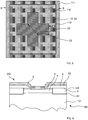
- the inventive RC-IGBT may comprise a fifth layer 5', formed as trench gate electrode as shown in FIG 9 .
- the trench gate electrode is arranged in the same plane as the fourth layer 4 and adjacent to the third layer 3, separated from each other by a first insulating layer 61, which also separates the fifth layer 5' from the base layer 101.
- a second insulating layer 62 is arranged on top of the fifth layer 5' formed as a trench gate electrode, thus insulating the fifth layer 5' from the first electrical contact 8.
- the n type first layer 1 comprises at least one or a plurality of first regions 10, wherein each first region 10 has a first region width 11.
- the first layer 1 comprises a plurality of first regions 10.
- the p type second layer 2 comprises at least one or a plurality of second regions 20 and at least one or a plurality of third regions 22, wherein each second region 20 has a second region width 21 and the third region 22 has a third region width 23.
- any of the first, second and third regions has a region width and a region area, which is surrounded by a region border.
- a shortest distance is the minimum length between a point within said region area and a point on the region border.
- the region width is measured in a plane parallel to the collector side 103.
- Each region width in this exemplary embodiment is defined as two times the maximum value of any shortest distance within said region.
- FIG 4 shows a cut through the first and second layer 1, 2 along the line B - B from FIG 3 .
- This line is also indicated in FIG 4 in order to show that the RC-IGBT does not have the same structure for the first and second layer 1, 2 over the whole plane of the wafer 100.
- the first and second layer 1, 2 only comprises first and second regions 10, 20 as shown in FIG 4 and 5 and which are also present in the FIG 6, 7 and 8 e.g. along the line B - B.
- the first and second layer 1, 2 comprise a third region 22, which form a pilot region.
- Each third region area is an area, in which any two first regions 10 have a distance bigger than two times the base layer thickness 102. That means that the third region 22 may be enclosed by first regions 10 which have a smaller distance to each other, but across the third region area, the distance between any two first regions 10 has to be larger than two times the base layer thickness 102. In other preferred embodiments, each third region area is an area, in which any two first regions 10 have a distance bigger than 2.5, in particular 3 times the base layer thickness 102.
- the at least one second region is that part of the second layer 2, which is not the at least one third region 22.
- the third region 22, i.e. the p doped area, in which any two first regions 10 have a distance bigger than two times the base layer thickness 102, is arranged in the central part of the active region in such a way that there is a minimum distance between the third region border to the active region border of at least once the base layer thickness 102, in particular twice the base layer thickness 102.
- the sum of the areas of the at least one third region 22 is between 10 % and 30 % of the active region 110.
- each first region width 11 is smaller than the base layer thickness 102.
- the second regions 20 and the first regions 10 form shorted regions.
- the second regions 20 are regions of the second conductivity type, which are not a third region 22.
- at least one second region width 21 is equal to or larger than once the base layer thickness 102, in particular each second region width 21 is equal to or larger than the base layer thickness 102, and each first region width 11 is smaller than the base layer thickness 102.
- the total area of the second and third regions 20, 22 to total area of the wafer 100 is between 70 % up to 90 %. In such a device the total area of the first regions 10 to total area of the wafer 100 is between 10 % up to 30 %.
- the sum of the areas of the at least one third region 22 is between 15 to 25 % and exemplarily about 20 % to the active region.
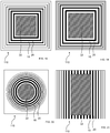
- Typical designs for the first and second regions 10, 20 are a stripe design (as shown in FIG 4 or 5 ) or a design, the third region is surrounded by the first and second regions and in which the first and second regions are self-contained shapes with an outer shape which enclose each other.
- the first regions 10 may be in exemplary embodiments of a square, rectangular or circular outer shape (the regions being formed as rings, which enclose one another).
- any appropriate design may be used for the first and second regions.
- the widths 11, 21 of the shorted first and/or second regions 10, 20 can be constant over the whole wafer area so that the first and third regions 10, 20 are arranged in a regular geometrical manner over the wafer 100 as e.g. shown in the FIG.s 4 and 5 , but their widths may also vary over the wafer 100.
- the second regions 20 being formed as stripes, the stripes can be surrounded be first regions as shown in Fig. 4 and 5 , but the first and second regions can also extend from one side of the border of the active region to the other as shown in FIG. 21 .
- the termination region 111 in which typically first and second regions 10, 20 are arranged, but alternatively this region may also consist of an n doped region or of a p doped region, surrounds the active region 110.
- the widths 21 of the second regions 20 may vary over the wafer 100 such that the widths of the second regions decrease from that second region, which is arranged closest to the border of the at least one third region, towards the border of the active region.
- the second regions are shown in these figures as a black line.
- the widths 11 of the first regions 10 may be constant ( FIG. 18 ) or it may vary, e.g. it may also decrease towards the border of the active region ( FIG. 19 ).
- the second regions may have the same design of the region border as the third region, but with larger dimensions.
- the second regions are squares, which surround the third region. Fig.
- the 20 shows exemplarily the third and second regions as circles.
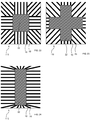
- Fig. 21 shows the regions as stripes.
- the first and second regions in the active region fulfill the geometrical rules given above.
- the decrease of the widths of the second regions may be present in only one direction (e.g. the direction of the width, i.e. the direction perpendicular to the length direction of the rectangles or stripes), whereas in another direction the width may be constant (length direction of the rectangles).
- the direction is measured in a plane parallel to the collector side 103.
- the initial snap-back is removed.
- a secondary snap-back may be present when these p doped regions are turned on one after the other and cause negative resistance jumps in the on-state characteristics.
- the third region 22 consists of a single region (as shown in the figures 6, 7 , 8 , 11 , 12 and 13 ).
- the third region may alternatively also comprise a plurality of regions, which are separated from each other by at most twice the base layer thickness, in particular by at most once the base layer thickness ( Fig. 14, 15 , 16 ).
- typically first regions are arranged between two regions belonging to the third region or at least the intermediate space comprises first regions, i.e. the intermediated space comprises first and second regions.
- the first regions 10 are arranged as stripes over the wafer 100.
- a plurality of stripes is arranged in a row and a plurality of such rows are arranged in columns within the active region 110.
- the third region 22 is connected to each second region 20 within the active region 110.
- the third region or regions 22 has in another preferred embodiment a square, rectangular, circular, star, diamond, tri-star or polygonal shape like a hexagon or another polyangular design.
- FIG 6 shows such a third region 22 with a square shape
- FIG 7 shows a third region 22 with a circular shape
- the first and second regions 10, 20 are only indicated by hatching of the area designated with 10, 20 for clarity reasons, but the hatched area is meant to be an area of alternating first and second regions 10, 20 as e.g. shown in fig. 4 and 5 .
- a shortest distance is the minimum length between a point within said region area and a point on said region border.
- the maximum value of any shortest distance within said region is for a square design ( FIG 6 ) the distance between the central point of the square to the middle point of any of the border lines. This is the longest distance to equalize charge during switching of the device.
- the region width is defined as two times this maximum value, i.e. the width is the length of the edge of the square.
- the third region width 23 corresponds to the diameter of the third region (again the maximum value is measured from the central point of the circle to any point on the border of the circular third region.
- the heat distribution can be improved, because the heat produced in this IGBT area without the necessity of increasing the size of the third region 22.
- Star shape shall mean any central area of a region, which is surrounded by protrusions (fingers) with at least three such protrusions.
- a cross as shown in fig. 8 is formed by four such protrusions.
- another number of fingers than four can be used in a star design as three fingers in a triangle (three armed star or tri-star shape) or five or more fingers in the star design.
- fingers shall be understood as areas, in which the width is smaller than the length of that area.
- Such fingers can be formed as a cross ( fig. 8 ), but of course also another number of fingers than 4 can be used as three fingers in a triangle or 5 or more fingers in a star design.
- FIG 8 show the second pilot region 22 in form of a cross.
- the cross is hypothetically divided into four outer rectangles and a central rectangle.
- the maximum value of any shortest distance between a point within the cross region to the border of the cross region exists from the middle point of the central rectangle of the cross to one of the four points, on which two adjacent outer rectangles adjoin.
- the third region width 23, which is two times this maximum value, is shown as a dashed line.
- the maximum value is the longest way an electron or hole has to flow in order to charge or discharge the region if the device is switched between on/off or vice versa.
- Fig. 22 shows another exemplary embodiment of the inventive device, in which the third region 22 in square design is connected to second regions 20, which extend to the border of the active region 110. In case of the device comprising a plurality of third regions 22, these regions 22 are interconnected to one another by second regions 20. In another exemplary embodiment, the second regions 20, which expand to the border of the active region 110, are arranged radial between the at least third region and the border of the active region. By “radial” it is meant that the second regions are arranged star like around the third region 22 such that the second regions are short connections to the border of the active region.
- Fig. 23 shows the third region in a cross design and Fig. 24 in a stripe design.
- the second regions radiate from the third region border to the active region border and thus form shortest connections.
- the second regions extend such that the distance between the first regions does not get to large (i.e. the geometrical rules for first region distances are fulfilled).
- the initial snap-back is removed. Due to the smaller size of the second regions a secondary snap-back may be present when these p doped regions are turned on one after the other and cause negative resistance jumps in the on-state characteristics, if the second regions are disconnected from the third region.
- the third region connected to second regions, and by radial extending the second regions between the third region to the border of the active region, the snap-back effect is further lowered or even avoided.
- the RC-IGBT 10 may further comprise an n type seventh layer 7, which is arranged between the base layer 101 and the first and second layer 1, 2 respectively, and which seventh layer 7 has a higher doping concentration than the base layer 101.
- the seventh layer 7 has preferably a maximum doping concentration of at most 1 ⁇ 10 16 cm -3 .
- an eighth n doped layer 41 is arranged between the fourth layer 4 and the base layer 101 for having lower on-state losses.
- the eighth layer 41 separates the fourth layer 4 from the base layer 101 and it has higher doping concentration than the base layer 101.
- the eighth layer 41 can be present in planar gate designs as well as in trench gate designs.
- the conductivity types of the layers are switched, i.e. all layers of the first conductivity type are p type (e.g. the base layer 101) and all layers of the second conductivity type are n type (e.g. the fourth layer 4).
- the inventive reverse-conducting semiconductor device 200 can for example be used in a converter.
Priority Applications (4)
| Application Number | Priority Date | Filing Date | Title |
|---|---|---|---|
| EP10154064.9A EP2249392B1 (en) | 2009-04-29 | 2010-02-19 | Reverse-conducting semiconductor device |
| US12/770,451 US8212283B2 (en) | 2009-04-29 | 2010-04-29 | Reverse-conducting semiconductor device |
| CN201010175167.3A CN101877352B (zh) | 2009-04-29 | 2010-04-29 | 反向导通半导体器件 |
| JP2010104715A JP5697891B2 (ja) | 2009-04-29 | 2010-04-30 | 逆導電半導体デバイス |
Applications Claiming Priority (2)
| Application Number | Priority Date | Filing Date | Title |
|---|---|---|---|
| EP09159009 | 2009-04-29 | ||
| EP10154064.9A EP2249392B1 (en) | 2009-04-29 | 2010-02-19 | Reverse-conducting semiconductor device |
Publications (3)
| Publication Number | Publication Date |
|---|---|
| EP2249392A2 EP2249392A2 (en) | 2010-11-10 |
| EP2249392A3 EP2249392A3 (en) | 2011-08-03 |
| EP2249392B1 true EP2249392B1 (en) | 2020-05-20 |
Family
ID=40972804
Family Applications (1)
| Application Number | Title | Priority Date | Filing Date |
|---|---|---|---|
| EP10154064.9A Active EP2249392B1 (en) | 2009-04-29 | 2010-02-19 | Reverse-conducting semiconductor device |
Country Status (5)
| Country | Link |
|---|---|
| US (1) | US8212283B2 (zh) |
| EP (1) | EP2249392B1 (zh) |
| JP (1) | JP5697891B2 (zh) |
| CN (1) | CN101877352B (zh) |
| DK (1) | DK2249392T3 (zh) |
Families Citing this family (40)
| Publication number | Priority date | Publication date | Assignee | Title |
|---|---|---|---|---|
| EP2339613B1 (en) | 2009-12-22 | 2015-08-19 | ABB Technology AG | Power semiconductor device and method for producing same |
| US8729914B2 (en) * | 2010-11-10 | 2014-05-20 | Infineon Technologies Ag | Detection of the conduction state of an RC-IGBT |
| KR101303422B1 (ko) * | 2011-03-28 | 2013-09-05 | 주식회사 엘지실트론 | 단결정 잉곳의 제조방법 및 이에 의해 제조된 단결정 잉곳과 웨이퍼 |
| JP6037495B2 (ja) * | 2011-10-17 | 2016-12-07 | ローム株式会社 | 半導体装置およびその製造方法 |
| JP5742711B2 (ja) * | 2011-12-28 | 2015-07-01 | 株式会社デンソー | 半導体装置 |
| US9018674B2 (en) * | 2012-04-06 | 2015-04-28 | Infineon Technologies Ag | Reverse conducting insulated gate bipolar transistor |
| WO2014086016A1 (zh) * | 2012-12-06 | 2014-06-12 | 中国科学院微电子研究所 | Rc-igbt及其制作方法 |
| JP6234696B2 (ja) * | 2013-04-16 | 2017-11-22 | ローム株式会社 | 半導体装置 |
| GB2520617B (en) | 2013-10-22 | 2020-12-30 | Abb Schweiz Ag | RC-IGBT with freewheeling SiC diode |
| CN105830221B (zh) * | 2013-12-23 | 2017-11-03 | Abb 技术有限公司 | 反向传导半导体装置 |
| EP3105791B1 (en) | 2014-02-14 | 2021-05-26 | ABB Power Grids Switzerland AG | Semiconductor module with two auxiliary emitter conductor paths |
| US9159819B2 (en) | 2014-02-20 | 2015-10-13 | Infineon Technologies Ag | Semiconductor device and RC-IGBT with zones directly adjoining a rear side electrode |
| CN104979379A (zh) * | 2014-04-03 | 2015-10-14 | 中国科学院微电子研究所 | 半导体器件的集电极结构及ti-igbt |
| WO2016001182A2 (en) | 2014-06-30 | 2016-01-07 | Abb Technology Ag | Semiconductor device |
| CN107004578B (zh) * | 2014-09-15 | 2020-01-24 | Abb瑞士股份有限公司 | 用于制造包括薄半导体晶圆的半导体器件的方法 |
| EP3238260B1 (en) * | 2014-12-23 | 2020-03-25 | ABB Power Grids Switzerland AG | Reverse-conducting semiconductor device |
| CN105448972B (zh) * | 2014-12-25 | 2019-04-19 | 深圳深爱半导体股份有限公司 | 反向导通绝缘栅双极型晶体管 |
| EP3180799B1 (en) | 2015-06-09 | 2018-12-26 | ABB Schweiz AG | Silicon carbide power semiconductor device comprising an edge termination and method for manufacturing said edge termination |
| EP3154091A1 (en) | 2015-10-07 | 2017-04-12 | ABB Technology AG | Reverse-conducting semiconductor device |
| EP3176812A1 (en) | 2015-12-02 | 2017-06-07 | ABB Schweiz AG | Semiconductor device and method for manufacturing such a semiconductor device |
| JP6454447B2 (ja) | 2015-12-02 | 2019-01-16 | アーベーベー・シュバイツ・アーゲー | 半導体装置の製造方法 |
| JP6817777B2 (ja) * | 2015-12-16 | 2021-01-20 | ローム株式会社 | 半導体装置 |
| EP3223316A1 (en) | 2016-03-24 | 2017-09-27 | ABB Technology AG | Wide bandgap power semiconductor device and method for manufacturing such a device |
| DE102016110035B4 (de) | 2016-05-31 | 2020-09-10 | Infineon Technologies Ag | Elektrische Baugruppe, die eine bipolare Schaltvorrichtung und einen selbstleitenden Transistor mit breiter Bandlücke umfasst, und eine elektrische Baugruppe, die eine bipolare Schaltvorrichtung und einen selbstleitenden Junction-Feldeffekttransistor umfasst, der einen Halbleiterbereich aus Siliziumcarbid umfasst |
| EP3255676A1 (en) | 2016-06-09 | 2017-12-13 | ABB Schweiz AG | Vertical power semiconductor device and method for operating such a device |
| JP6854598B2 (ja) | 2016-07-06 | 2021-04-07 | ローム株式会社 | 半導体装置 |
| EP3306672A1 (en) | 2016-10-07 | 2018-04-11 | ABB Schweiz AG | Semiconductor device |
| EP3539215B1 (en) | 2016-11-14 | 2020-01-22 | ABB Schweiz AG | Switching of paralleled reverse conducting igbt and wide bandgap switch |
| JP6854654B2 (ja) | 2017-01-26 | 2021-04-07 | ローム株式会社 | 半導体装置 |
| US10439038B2 (en) | 2017-02-09 | 2019-10-08 | Kabushiki Kaisha Toshiba | Semiconductor device and electrical apparatus |
| CN108417549B (zh) | 2017-02-09 | 2021-09-24 | 株式会社东芝 | 半导体装置及电气设备 |
| US10446539B2 (en) * | 2017-02-24 | 2019-10-15 | Nxp B.V. | Electrostatic discharge (ESD) protection device and method for operating an ESD protection device |
| DE112018008221T5 (de) * | 2018-12-19 | 2021-09-02 | Mitsubishi Electric Corporation | Halbleitervorrichtung |
| CN109728085B (zh) * | 2018-12-29 | 2021-10-22 | 安建科技(深圳)有限公司 | 一种逆导型绝缘栅双极性晶体管 |
| CN109830531A (zh) * | 2019-01-15 | 2019-05-31 | 上海华虹宏力半导体制造有限公司 | Rc-igbt器件及其制造方法 |
| GB2584698B (en) | 2019-06-12 | 2022-09-14 | Mqsemi Ag | Non-punch-through reverse-conducting power semiconductor device and method for producing same |
| JP7404702B2 (ja) | 2019-08-09 | 2023-12-26 | 富士電機株式会社 | 半導体装置 |
| CN112201688B (zh) * | 2020-08-25 | 2023-04-07 | 株洲中车时代半导体有限公司 | 逆导型igbt芯片 |
| CN114335157B (zh) * | 2021-12-17 | 2024-01-19 | 贵州振华风光半导体股份有限公司 | 一种纵向双极结型晶体管版图结构 |
| JP2023101242A (ja) * | 2022-01-07 | 2023-07-20 | 株式会社東芝 | 半導体装置 |
Citations (1)
| Publication number | Priority date | Publication date | Assignee | Title |
|---|---|---|---|---|
| EP2184781A1 (en) * | 2008-11-05 | 2010-05-12 | ABB Technology AG | Reverse-conducting semiconductor device |
Family Cites Families (10)
| Publication number | Priority date | Publication date | Assignee | Title |
|---|---|---|---|---|
| JPH0828506B2 (ja) | 1988-11-07 | 1996-03-21 | 三菱電機株式会社 | 半導体装置およびその製造方法 |
| DE59502494D1 (de) | 1994-12-02 | 1998-07-16 | Walter Steiner | Wäschetrockner |
| DE10250575B4 (de) * | 2002-10-30 | 2010-04-15 | Infineon Technologies Ag | IGBT mit monolithisch integrierter antiparalleler Diode |
| JP2005057235A (ja) * | 2003-07-24 | 2005-03-03 | Mitsubishi Electric Corp | 絶縁ゲート型バイポーラトランジスタ及びその製造方法、並びに、インバータ回路 |
| JP4415767B2 (ja) | 2004-06-14 | 2010-02-17 | サンケン電気株式会社 | 絶縁ゲート型半導体素子、及びその製造方法 |
| DE102005019178A1 (de) * | 2005-04-25 | 2006-11-02 | Infineon Technologies Ag | Halbleiterbauelement, insbesondere rückwärts leitender IGBT |
| JP5157201B2 (ja) * | 2006-03-22 | 2013-03-06 | 株式会社デンソー | 半導体装置 |
| DE102006050338B4 (de) | 2006-10-25 | 2011-12-29 | Infineon Technologies Austria Ag | Halbleiterbauelement mit verbessertem Speicherladung zu Dioden-Softness Trade-off |
| EP2086012A1 (en) | 2007-12-19 | 2009-08-05 | ABB Technology AG | Reverse-conducting insulated gate bipolar transistor and method for manufacturing such a reverse-conducting insulated gate bipolar transistor |
| EP2073271A1 (en) | 2007-12-19 | 2009-06-24 | ABB Technology AG | Reverse-conducting insulated gate bipolar transistor and method for manufacturing such a reverse-conducting insulated gate bipolar transistor |
-
2010
- 2010-02-19 EP EP10154064.9A patent/EP2249392B1/en active Active
- 2010-02-19 DK DK10154064.9T patent/DK2249392T3/da active
- 2010-04-29 US US12/770,451 patent/US8212283B2/en active Active
- 2010-04-29 CN CN201010175167.3A patent/CN101877352B/zh active Active
- 2010-04-30 JP JP2010104715A patent/JP5697891B2/ja active Active
Patent Citations (1)
| Publication number | Priority date | Publication date | Assignee | Title |
|---|---|---|---|---|
| EP2184781A1 (en) * | 2008-11-05 | 2010-05-12 | ABB Technology AG | Reverse-conducting semiconductor device |
Also Published As
| Publication number | Publication date |
|---|---|
| JP2010263215A (ja) | 2010-11-18 |
| CN101877352A (zh) | 2010-11-03 |
| EP2249392A2 (en) | 2010-11-10 |
| JP5697891B2 (ja) | 2015-04-08 |
| EP2249392A3 (en) | 2011-08-03 |
| US20100276727A1 (en) | 2010-11-04 |
| DK2249392T3 (da) | 2020-08-17 |
| US8212283B2 (en) | 2012-07-03 |
| CN101877352B (zh) | 2015-09-09 |
Similar Documents
| Publication | Publication Date | Title |
|---|---|---|
| EP2249392B1 (en) | Reverse-conducting semiconductor device | |
| US10109725B2 (en) | Reverse-conducting semiconductor device | |
| EP2345081B1 (en) | Reverse-conducting semiconductor device | |
| CN108933170B (zh) | 窄的有源单元ie型沟槽栅极igbt及其制造方法 | |
| US9153575B2 (en) | Semiconductor device | |
| JP5900503B2 (ja) | 半導体装置 | |
| JP5805756B2 (ja) | パワー半導体デバイス | |
| EP2622639B1 (en) | Reverse-conducting power semiconductor device | |
| EP2667418A2 (en) | Semiconductor device | |
| US9553086B2 (en) | Reverse-conducting semiconductor device | |
| JP2018530916A (ja) | フラットゲート転流型サイリスタ | |
| JP5760320B2 (ja) | 半導体装置 | |
| WO2016001182A2 (en) | Semiconductor device | |
| EP4101008B1 (en) | Reverse conducting power semiconductor device and method for manufacturing the same | |
| JP7246423B2 (ja) | 半導体装置 | |
| JP2007180338A (ja) | 半導体装置 | |
| JP2013251464A (ja) | 半導体装置 |
Legal Events
| Date | Code | Title | Description |
|---|---|---|---|
| PUAI | Public reference made under article 153(3) epc to a published international application that has entered the european phase |
Free format text: ORIGINAL CODE: 0009012 |
|
| AK | Designated contracting states |
Kind code of ref document: A2 Designated state(s): AT BE BG CH CY CZ DE DK EE ES FI FR GB GR HR HU IE IS IT LI LT LU LV MC MK MT NL NO PL PT RO SE SI SK SM TR |
|
| AX | Request for extension of the european patent |
Extension state: AL BA RS |
|
| PUAL | Search report despatched |
Free format text: ORIGINAL CODE: 0009013 |
|
| AK | Designated contracting states |
Kind code of ref document: A3 Designated state(s): AT BE BG CH CY CZ DE DK EE ES FI FR GB GR HR HU IE IS IT LI LT LU LV MC MK MT NL NO PL PT RO SE SI SK SM TR |
|
| AX | Request for extension of the european patent |
Extension state: AL BA RS |
|
| RIC1 | Information provided on ipc code assigned before grant |
Ipc: H01L 21/331 20060101ALN20110628BHEP Ipc: H01L 29/739 20060101ALI20110628BHEP Ipc: H01L 29/08 20060101AFI20110628BHEP |
|
| 17P | Request for examination filed |
Effective date: 20120203 |
|
| STAA | Information on the status of an ep patent application or granted ep patent |
Free format text: STATUS: EXAMINATION IS IN PROGRESS |
|
| 17Q | First examination report despatched |
Effective date: 20161205 |
|
| RAP1 | Party data changed (applicant data changed or rights of an application transferred) |
Owner name: ABB SCHWEIZ AG |
|
| RIN1 | Information on inventor provided before grant (corrected) |
Inventor name: RAHIMO, MUNAF Inventor name: STORASTA, LIUTAURAS Inventor name: VON ARX, CHRISTOPH Inventor name: KOPTA, ARNOST Inventor name: SCHNELL, RAFFAEL |
|
| GRAP | Despatch of communication of intention to grant a patent |
Free format text: ORIGINAL CODE: EPIDOSNIGR1 |
|
| STAA | Information on the status of an ep patent application or granted ep patent |
Free format text: STATUS: GRANT OF PATENT IS INTENDED |
|
| INTG | Intention to grant announced |
Effective date: 20190919 |
|
| GRAS | Grant fee paid |
Free format text: ORIGINAL CODE: EPIDOSNIGR3 |
|
| GRAL | Information related to payment of fee for publishing/printing deleted |
Free format text: ORIGINAL CODE: EPIDOSDIGR3 |
|
| GRAS | Grant fee paid |
Free format text: ORIGINAL CODE: EPIDOSNIGR3 |
|
| RIN1 | Information on inventor provided before grant (corrected) |
Inventor name: SCHNELL, RAFFAEL Inventor name: VON ARX, CHRISTOPH Inventor name: RAHIMO, MUNAF Inventor name: KOPTA, ARNOST Inventor name: STORASTA, LIUTAURAS |
|
| RAP1 | Party data changed (applicant data changed or rights of an application transferred) |
Owner name: ABB POWER GRIDS SWITZERLAND AG |
|
| GRAA | (expected) grant |
Free format text: ORIGINAL CODE: 0009210 |
|
| STAA | Information on the status of an ep patent application or granted ep patent |
Free format text: STATUS: THE PATENT HAS BEEN GRANTED |
|
| AK | Designated contracting states |
Kind code of ref document: B1 Designated state(s): AT BE BG CH CY CZ DE DK EE ES FI FR GB GR HR HU IE IS IT LI LT LU LV MC MK MT NL NO PL PT RO SE SI SK SM TR |
|
| REG | Reference to a national code |
Ref country code: GB Ref legal event code: FG4D |
|
| REG | Reference to a national code |
Ref country code: CH Ref legal event code: EP |
|
| REG | Reference to a national code |
Ref country code: DE Ref legal event code: R096 Ref document number: 602010064385 Country of ref document: DE |
|
| REG | Reference to a national code |
Ref country code: AT Ref legal event code: REF Ref document number: 1273187 Country of ref document: AT Kind code of ref document: T Effective date: 20200615 |
|
| REG | Reference to a national code |
Ref country code: DK Ref legal event code: T3 Effective date: 20200811 |
|
| REG | Reference to a national code |
Ref country code: SE Ref legal event code: TRGR |
|
| REG | Reference to a national code |
Ref country code: LT Ref legal event code: MG4D |
|
| REG | Reference to a national code |
Ref country code: NL Ref legal event code: MP Effective date: 20200520 |
|
| PG25 | Lapsed in a contracting state [announced via postgrant information from national office to epo] |
Ref country code: LT Free format text: LAPSE BECAUSE OF FAILURE TO SUBMIT A TRANSLATION OF THE DESCRIPTION OR TO PAY THE FEE WITHIN THE PRESCRIBED TIME-LIMIT Effective date: 20200520 Ref country code: PT Free format text: LAPSE BECAUSE OF FAILURE TO SUBMIT A TRANSLATION OF THE DESCRIPTION OR TO PAY THE FEE WITHIN THE PRESCRIBED TIME-LIMIT Effective date: 20200921 Ref country code: IS Free format text: LAPSE BECAUSE OF FAILURE TO SUBMIT A TRANSLATION OF THE DESCRIPTION OR TO PAY THE FEE WITHIN THE PRESCRIBED TIME-LIMIT Effective date: 20200920 Ref country code: FI Free format text: LAPSE BECAUSE OF FAILURE TO SUBMIT A TRANSLATION OF THE DESCRIPTION OR TO PAY THE FEE WITHIN THE PRESCRIBED TIME-LIMIT Effective date: 20200520 Ref country code: NO Free format text: LAPSE BECAUSE OF FAILURE TO SUBMIT A TRANSLATION OF THE DESCRIPTION OR TO PAY THE FEE WITHIN THE PRESCRIBED TIME-LIMIT Effective date: 20200820 Ref country code: GR Free format text: LAPSE BECAUSE OF FAILURE TO SUBMIT A TRANSLATION OF THE DESCRIPTION OR TO PAY THE FEE WITHIN THE PRESCRIBED TIME-LIMIT Effective date: 20200821 |
|
| PG25 | Lapsed in a contracting state [announced via postgrant information from national office to epo] |
Ref country code: BG Free format text: LAPSE BECAUSE OF FAILURE TO SUBMIT A TRANSLATION OF THE DESCRIPTION OR TO PAY THE FEE WITHIN THE PRESCRIBED TIME-LIMIT Effective date: 20200820 Ref country code: LV Free format text: LAPSE BECAUSE OF FAILURE TO SUBMIT A TRANSLATION OF THE DESCRIPTION OR TO PAY THE FEE WITHIN THE PRESCRIBED TIME-LIMIT Effective date: 20200520 Ref country code: HR Free format text: LAPSE BECAUSE OF FAILURE TO SUBMIT A TRANSLATION OF THE DESCRIPTION OR TO PAY THE FEE WITHIN THE PRESCRIBED TIME-LIMIT Effective date: 20200520 |
|
| REG | Reference to a national code |
Ref country code: AT Ref legal event code: MK05 Ref document number: 1273187 Country of ref document: AT Kind code of ref document: T Effective date: 20200520 |
|
| PG25 | Lapsed in a contracting state [announced via postgrant information from national office to epo] |
Ref country code: NL Free format text: LAPSE BECAUSE OF FAILURE TO SUBMIT A TRANSLATION OF THE DESCRIPTION OR TO PAY THE FEE WITHIN THE PRESCRIBED TIME-LIMIT Effective date: 20200520 |
|
| PG25 | Lapsed in a contracting state [announced via postgrant information from national office to epo] |
Ref country code: RO Free format text: LAPSE BECAUSE OF FAILURE TO SUBMIT A TRANSLATION OF THE DESCRIPTION OR TO PAY THE FEE WITHIN THE PRESCRIBED TIME-LIMIT Effective date: 20200520 Ref country code: CZ Free format text: LAPSE BECAUSE OF FAILURE TO SUBMIT A TRANSLATION OF THE DESCRIPTION OR TO PAY THE FEE WITHIN THE PRESCRIBED TIME-LIMIT Effective date: 20200520 Ref country code: SM Free format text: LAPSE BECAUSE OF FAILURE TO SUBMIT A TRANSLATION OF THE DESCRIPTION OR TO PAY THE FEE WITHIN THE PRESCRIBED TIME-LIMIT Effective date: 20200520 Ref country code: IT Free format text: LAPSE BECAUSE OF FAILURE TO SUBMIT A TRANSLATION OF THE DESCRIPTION OR TO PAY THE FEE WITHIN THE PRESCRIBED TIME-LIMIT Effective date: 20200520 Ref country code: EE Free format text: LAPSE BECAUSE OF FAILURE TO SUBMIT A TRANSLATION OF THE DESCRIPTION OR TO PAY THE FEE WITHIN THE PRESCRIBED TIME-LIMIT Effective date: 20200520 Ref country code: AT Free format text: LAPSE BECAUSE OF FAILURE TO SUBMIT A TRANSLATION OF THE DESCRIPTION OR TO PAY THE FEE WITHIN THE PRESCRIBED TIME-LIMIT Effective date: 20200520 Ref country code: ES Free format text: LAPSE BECAUSE OF FAILURE TO SUBMIT A TRANSLATION OF THE DESCRIPTION OR TO PAY THE FEE WITHIN THE PRESCRIBED TIME-LIMIT Effective date: 20200520 |
|
| REG | Reference to a national code |
Ref country code: DE Ref legal event code: R097 Ref document number: 602010064385 Country of ref document: DE |
|
| PG25 | Lapsed in a contracting state [announced via postgrant information from national office to epo] |
Ref country code: SK Free format text: LAPSE BECAUSE OF FAILURE TO SUBMIT A TRANSLATION OF THE DESCRIPTION OR TO PAY THE FEE WITHIN THE PRESCRIBED TIME-LIMIT Effective date: 20200520 Ref country code: PL Free format text: LAPSE BECAUSE OF FAILURE TO SUBMIT A TRANSLATION OF THE DESCRIPTION OR TO PAY THE FEE WITHIN THE PRESCRIBED TIME-LIMIT Effective date: 20200520 |
|
| PLBE | No opposition filed within time limit |
Free format text: ORIGINAL CODE: 0009261 |
|
| STAA | Information on the status of an ep patent application or granted ep patent |
Free format text: STATUS: NO OPPOSITION FILED WITHIN TIME LIMIT |
|
| 26N | No opposition filed |
Effective date: 20210223 |
|
| PG25 | Lapsed in a contracting state [announced via postgrant information from national office to epo] |
Ref country code: SI Free format text: LAPSE BECAUSE OF FAILURE TO SUBMIT A TRANSLATION OF THE DESCRIPTION OR TO PAY THE FEE WITHIN THE PRESCRIBED TIME-LIMIT Effective date: 20200520 |
|
| PG25 | Lapsed in a contracting state [announced via postgrant information from national office to epo] |
Ref country code: MC Free format text: LAPSE BECAUSE OF FAILURE TO SUBMIT A TRANSLATION OF THE DESCRIPTION OR TO PAY THE FEE WITHIN THE PRESCRIBED TIME-LIMIT Effective date: 20200520 |
|
| REG | Reference to a national code |
Ref country code: BE Ref legal event code: MM Effective date: 20210228 |
|
| PG25 | Lapsed in a contracting state [announced via postgrant information from national office to epo] |
Ref country code: LU Free format text: LAPSE BECAUSE OF NON-PAYMENT OF DUE FEES Effective date: 20210219 |
|
| PG25 | Lapsed in a contracting state [announced via postgrant information from national office to epo] |
Ref country code: IE Free format text: LAPSE BECAUSE OF NON-PAYMENT OF DUE FEES Effective date: 20210219 |
|
| REG | Reference to a national code |
Ref country code: DE Ref legal event code: R081 Ref document number: 602010064385 Country of ref document: DE Owner name: HITACHI ENERGY SWITZERLAND AG, CH Free format text: FORMER OWNER: ABB POWER GRIDS SWITZERLAND AG, BADEN, CH Ref country code: DE Ref legal event code: R081 Ref document number: 602010064385 Country of ref document: DE Owner name: HITACHI ENERGY LTD, CH Free format text: FORMER OWNER: ABB POWER GRIDS SWITZERLAND AG, BADEN, CH |
|
| PG25 | Lapsed in a contracting state [announced via postgrant information from national office to epo] |
Ref country code: BE Free format text: LAPSE BECAUSE OF NON-PAYMENT OF DUE FEES Effective date: 20210228 |
|
| PGFP | Annual fee paid to national office [announced via postgrant information from national office to epo] |
Ref country code: FR Payment date: 20230220 Year of fee payment: 14 Ref country code: DK Payment date: 20230220 Year of fee payment: 14 Ref country code: CH Payment date: 20230307 Year of fee payment: 14 |
|
| PG25 | Lapsed in a contracting state [announced via postgrant information from national office to epo] |
Ref country code: HU Free format text: LAPSE BECAUSE OF FAILURE TO SUBMIT A TRANSLATION OF THE DESCRIPTION OR TO PAY THE FEE WITHIN THE PRESCRIBED TIME-LIMIT; INVALID AB INITIO Effective date: 20100219 Ref country code: CY Free format text: LAPSE BECAUSE OF FAILURE TO SUBMIT A TRANSLATION OF THE DESCRIPTION OR TO PAY THE FEE WITHIN THE PRESCRIBED TIME-LIMIT Effective date: 20200520 |
|
| PGFP | Annual fee paid to national office [announced via postgrant information from national office to epo] |
Ref country code: SE Payment date: 20230216 Year of fee payment: 14 Ref country code: GB Payment date: 20230220 Year of fee payment: 14 Ref country code: DE Payment date: 20230216 Year of fee payment: 14 |
|
| P01 | Opt-out of the competence of the unified patent court (upc) registered |
Effective date: 20230527 |
|
| REG | Reference to a national code |
Ref country code: DE Ref legal event code: R082 Ref document number: 602010064385 Country of ref document: DE Representative=s name: DENNEMEYER & ASSOCIATES S.A., DE Ref country code: DE Ref legal event code: R081 Ref document number: 602010064385 Country of ref document: DE Owner name: HITACHI ENERGY LTD, CH Free format text: FORMER OWNER: HITACHI ENERGY SWITZERLAND AG, BADEN, CH |