EP2243156B1 - Procédés et appareils pour la manipulation de plaquettes de grand diamètre - Google Patents
Procédés et appareils pour la manipulation de plaquettes de grand diamètre Download PDFInfo
- Publication number
- EP2243156B1 EP2243156B1 EP09700304.0A EP09700304A EP2243156B1 EP 2243156 B1 EP2243156 B1 EP 2243156B1 EP 09700304 A EP09700304 A EP 09700304A EP 2243156 B1 EP2243156 B1 EP 2243156B1
- Authority
- EP
- European Patent Office
- Prior art keywords
- wafer
- door
- container
- extending
- wafers
- Prior art date
- Legal status (The legal status is an assumption and is not a legal conclusion. Google has not performed a legal analysis and makes no representation as to the accuracy of the status listed.)
- Not-in-force
Links
Images


Classifications
-
- H—ELECTRICITY
- H01—ELECTRIC ELEMENTS
- H01L—SEMICONDUCTOR DEVICES NOT COVERED BY CLASS H10
- H01L21/00—Processes or apparatus adapted for the manufacture or treatment of semiconductor or solid state devices or of parts thereof
- H01L21/67—Apparatus specially adapted for handling semiconductor or electric solid state devices during manufacture or treatment thereof; Apparatus specially adapted for handling wafers during manufacture or treatment of semiconductor or electric solid state devices or components ; Apparatus not specifically provided for elsewhere
- H01L21/673—Apparatus specially adapted for handling semiconductor or electric solid state devices during manufacture or treatment thereof; Apparatus specially adapted for handling wafers during manufacture or treatment of semiconductor or electric solid state devices or components ; Apparatus not specifically provided for elsewhere using specially adapted carriers or holders; Fixing the workpieces on such carriers or holders
- H01L21/6732—Vertical carrier comprising wall type elements whereby the substrates are horizontally supported, e.g. comprising sidewalls
-
- B—PERFORMING OPERATIONS; TRANSPORTING
- B65—CONVEYING; PACKING; STORING; HANDLING THIN OR FILAMENTARY MATERIAL
- B65D—CONTAINERS FOR STORAGE OR TRANSPORT OF ARTICLES OR MATERIALS, e.g. BAGS, BARRELS, BOTTLES, BOXES, CANS, CARTONS, CRATES, DRUMS, JARS, TANKS, HOPPERS, FORWARDING CONTAINERS; ACCESSORIES, CLOSURES, OR FITTINGS THEREFOR; PACKAGING ELEMENTS; PACKAGES
- B65D25/00—Details of other kinds or types of rigid or semi-rigid containers
- B65D25/02—Internal fittings
- B65D25/10—Devices to locate articles in containers
- B65D25/103—V-shaped elements, e.g. racks, protuberances projecting from a supporting surface, supporting the articles locally at its sides
-
- H—ELECTRICITY
- H01—ELECTRIC ELEMENTS
- H01L—SEMICONDUCTOR DEVICES NOT COVERED BY CLASS H10
- H01L21/00—Processes or apparatus adapted for the manufacture or treatment of semiconductor or solid state devices or of parts thereof
- H01L21/67—Apparatus specially adapted for handling semiconductor or electric solid state devices during manufacture or treatment thereof; Apparatus specially adapted for handling wafers during manufacture or treatment of semiconductor or electric solid state devices or components ; Apparatus not specifically provided for elsewhere
- H01L21/673—Apparatus specially adapted for handling semiconductor or electric solid state devices during manufacture or treatment thereof; Apparatus specially adapted for handling wafers during manufacture or treatment of semiconductor or electric solid state devices or components ; Apparatus not specifically provided for elsewhere using specially adapted carriers or holders; Fixing the workpieces on such carriers or holders
- H01L21/6735—Closed carriers
- H01L21/67383—Closed carriers characterised by substrate supports
-
- B—PERFORMING OPERATIONS; TRANSPORTING
- B65—CONVEYING; PACKING; STORING; HANDLING THIN OR FILAMENTARY MATERIAL
- B65D—CONTAINERS FOR STORAGE OR TRANSPORT OF ARTICLES OR MATERIALS, e.g. BAGS, BARRELS, BOTTLES, BOXES, CANS, CARTONS, CRATES, DRUMS, JARS, TANKS, HOPPERS, FORWARDING CONTAINERS; ACCESSORIES, CLOSURES, OR FITTINGS THEREFOR; PACKAGING ELEMENTS; PACKAGES
- B65D25/00—Details of other kinds or types of rigid or semi-rigid containers
- B65D25/28—Handles
-
- B—PERFORMING OPERATIONS; TRANSPORTING
- B65—CONVEYING; PACKING; STORING; HANDLING THIN OR FILAMENTARY MATERIAL
- B65D—CONTAINERS FOR STORAGE OR TRANSPORT OF ARTICLES OR MATERIALS, e.g. BAGS, BARRELS, BOTTLES, BOXES, CANS, CARTONS, CRATES, DRUMS, JARS, TANKS, HOPPERS, FORWARDING CONTAINERS; ACCESSORIES, CLOSURES, OR FITTINGS THEREFOR; PACKAGING ELEMENTS; PACKAGES
- B65D43/00—Lids or covers for rigid or semi-rigid containers
- B65D43/02—Removable lids or covers
-
- B—PERFORMING OPERATIONS; TRANSPORTING
- B65—CONVEYING; PACKING; STORING; HANDLING THIN OR FILAMENTARY MATERIAL
- B65D—CONTAINERS FOR STORAGE OR TRANSPORT OF ARTICLES OR MATERIALS, e.g. BAGS, BARRELS, BOTTLES, BOXES, CANS, CARTONS, CRATES, DRUMS, JARS, TANKS, HOPPERS, FORWARDING CONTAINERS; ACCESSORIES, CLOSURES, OR FITTINGS THEREFOR; PACKAGING ELEMENTS; PACKAGES
- B65D85/00—Containers, packaging elements or packages, specially adapted for particular articles or materials
- B65D85/30—Containers, packaging elements or packages, specially adapted for particular articles or materials for articles particularly sensitive to damage by shock or pressure
- B65D85/38—Containers, packaging elements or packages, specially adapted for particular articles or materials for articles particularly sensitive to damage by shock or pressure for delicate optical, measuring, calculating or control apparatus
-
- B—PERFORMING OPERATIONS; TRANSPORTING
- B65—CONVEYING; PACKING; STORING; HANDLING THIN OR FILAMENTARY MATERIAL
- B65D—CONTAINERS FOR STORAGE OR TRANSPORT OF ARTICLES OR MATERIALS, e.g. BAGS, BARRELS, BOTTLES, BOXES, CANS, CARTONS, CRATES, DRUMS, JARS, TANKS, HOPPERS, FORWARDING CONTAINERS; ACCESSORIES, CLOSURES, OR FITTINGS THEREFOR; PACKAGING ELEMENTS; PACKAGES
- B65D85/00—Containers, packaging elements or packages, specially adapted for particular articles or materials
- B65D85/70—Containers, packaging elements or packages, specially adapted for particular articles or materials for materials not otherwise provided for
-
- H—ELECTRICITY
- H01—ELECTRIC ELEMENTS
- H01L—SEMICONDUCTOR DEVICES NOT COVERED BY CLASS H10
- H01L21/00—Processes or apparatus adapted for the manufacture or treatment of semiconductor or solid state devices or of parts thereof
- H01L21/67—Apparatus specially adapted for handling semiconductor or electric solid state devices during manufacture or treatment thereof; Apparatus specially adapted for handling wafers during manufacture or treatment of semiconductor or electric solid state devices or components ; Apparatus not specifically provided for elsewhere
- H01L21/673—Apparatus specially adapted for handling semiconductor or electric solid state devices during manufacture or treatment thereof; Apparatus specially adapted for handling wafers during manufacture or treatment of semiconductor or electric solid state devices or components ; Apparatus not specifically provided for elsewhere using specially adapted carriers or holders; Fixing the workpieces on such carriers or holders
- H01L21/6735—Closed carriers
- H01L21/67369—Closed carriers characterised by shock absorbing elements, e.g. retainers or cushions
-
- H—ELECTRICITY
- H01—ELECTRIC ELEMENTS
- H01L—SEMICONDUCTOR DEVICES NOT COVERED BY CLASS H10
- H01L21/00—Processes or apparatus adapted for the manufacture or treatment of semiconductor or solid state devices or of parts thereof
- H01L21/67—Apparatus specially adapted for handling semiconductor or electric solid state devices during manufacture or treatment thereof; Apparatus specially adapted for handling wafers during manufacture or treatment of semiconductor or electric solid state devices or components ; Apparatus not specifically provided for elsewhere
- H01L21/673—Apparatus specially adapted for handling semiconductor or electric solid state devices during manufacture or treatment thereof; Apparatus specially adapted for handling wafers during manufacture or treatment of semiconductor or electric solid state devices or components ; Apparatus not specifically provided for elsewhere using specially adapted carriers or holders; Fixing the workpieces on such carriers or holders
- H01L21/6735—Closed carriers
- H01L21/67386—Closed carriers characterised by the construction of the closed carrier
-
- H—ELECTRICITY
- H01—ELECTRIC ELEMENTS
- H01L—SEMICONDUCTOR DEVICES NOT COVERED BY CLASS H10
- H01L21/00—Processes or apparatus adapted for the manufacture or treatment of semiconductor or solid state devices or of parts thereof
- H01L21/67—Apparatus specially adapted for handling semiconductor or electric solid state devices during manufacture or treatment thereof; Apparatus specially adapted for handling wafers during manufacture or treatment of semiconductor or electric solid state devices or components ; Apparatus not specifically provided for elsewhere
- H01L21/677—Apparatus specially adapted for handling semiconductor or electric solid state devices during manufacture or treatment thereof; Apparatus specially adapted for handling wafers during manufacture or treatment of semiconductor or electric solid state devices or components ; Apparatus not specifically provided for elsewhere for conveying, e.g. between different workstations
- H01L21/67763—Apparatus specially adapted for handling semiconductor or electric solid state devices during manufacture or treatment thereof; Apparatus specially adapted for handling wafers during manufacture or treatment of semiconductor or electric solid state devices or components ; Apparatus not specifically provided for elsewhere for conveying, e.g. between different workstations the wafers being stored in a carrier, involving loading and unloading
- H01L21/67769—Storage means
Claims (8)
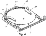
- Récipient de plaquettes semi-conductrices à ouverture avant (30) pour des plaquettes de grand diamètre (W) comprenant :une partie de récipient (40) ayant un côté gauche fermé (43), un côté droit fermé (44), une partie arrière fermée (45), une partie avant ouverte, et un intérieur ouvert (48) comprenant une pluralité de fentes pour recevoir et contenir les plaquettes (W) ;une porte (42) pouvant être fixée à la partie de récipient (40) pour fermer la partie avant ouverte et pouvant être sélectivement verrouillée sur la partie de récipient (40) ;la partie de récipient (40) comprenant un moyen pour loger les plaquettes de grand diamètre (W), ledit moyen pour loger les plaquettes de grand diamètre comprenant un dispositif de retenue de plaquettes arrière (420) à l'intérieur du récipient (30), et un dispositif de retenue de plaquettes avant (430) disposé sur une surface intérieure (407) de la porte (42),caractérisé par le dispositif de retenue de plaquettes arrière (420) et/ou le dispositif de retenue de plaquettes avant (430) qui comprennent une pluralité de fentes en forme de V (424 et/ou 434), dans lequel chaque fente en forme de V (424 et/ou 434) du dispositif de retenue de plaquettes arrière (420) et/ou du dispositif de retenue de plaquettes avant (430) comprend :une patte supérieure (612) s'étendant de manière angulaire vers le haut et ayant une surface de mise en prise de plaquette (611) s'étendant vers le haut dans la direction d'une plaquette mise en prise, etune patte inférieure (610) s'étendant de manière angulaire vers le bas et ayant une surface de mise en prise de plaquette (609) s'étendant vers le bas dans la direction de la plaquette mise en prise, l'extension vers le bas dans la direction de la plaquette mise en prise de la surface de mise en prise de plaquette de patte inférieure (609) étant plus longue que l'extension vers le haut dans la direction de la plaquette mise en prise de la surface de mise en prise de plaquette de patte supérieure (611), et la patte supérieure (612) surplombe la surface de mise en prise de plaquette de patte inférieure (609) définissant une partie de rebord inversé (614) s'étendant horizontalement avec une surface de rebord (613) orientée vers le bas.
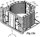
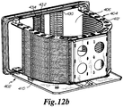
- Récipient selon la revendication 1, dans lequel le moyen pour loger les plaquettes de grand diamètre comprend des dispositifs de retenue de plaquettes (430, 432) disposés sur une surface intérieure (407) de la porte (42), les dispositifs de retenue de plaquettes (430, 432) comprenant une pluralité de supports de plaquettes (433) interconnectés s'étendant horizontalement, verticalement alignés, pour la mise en prise d'un bord périphérique avant des plaquettes lorsque la porte (42) est fixée sur le bâti de porte (60), chacun de la pluralité de supports de plaquettes (433) ayant une longueur, et chacun comprenant :une partie de base (460) fixée de manière immobile, sur le récipient (30) ;une partie de mise en prise de plaquette initiale (462) pouvant être déviée, etune partie intermédiaire (464) raccordant la partie de base (460) et la partie de mise en prise de plaquette (462), la partie intermédiaire (464) et la partie de mise en prise de plaquette initiale (462) pouvant être déviée étant en porte-à-faux à partir de la partie de base (460),dans laquelle des supports de plaquette (433) adjacents sont interconnectés entre eux le long des parties de base (460) respectives et ne sont pas raccordés le long des parties intermédiaires (464) respectives ou des parties de mise en prise de plaquette (462) ;dans lequel, lorsqu'elle est observée en profil, une patte supérieure (482) s'étend vers l'extérieur à partir de la porte (42) et vers le haut, et une patte inférieure (480) s'étend vers l'extérieur à partir de la porte (42) et définissant, vers le bas, une partie généralement en forme de V, avec un sommet comprenant une surface de mise en prise de plaquette en forme de V avec un sommet, la patte supérieure (482) et la patte inférieure (480) étendant la longueur du support de plaquette, et la partie intermédiaire (464) ayant une ouverture allongée (470) à travers cette dernière fournissant une paire de doigts (472) s'étendant horizontalement entre la partie de base (460) et la partie de mise en prise de plaquette (462) pouvant être déviée.
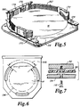
- Récipient selon la revendication 1 ou 2, dans lequel le moyen pour loger des plaquettes de grand diamètre comprend une paire de colonnes de supports de plaquette (70) interconnectés, verticalement alignés dans l'intérieur ouvert (48), l'une de ladite paire étant à proximité du côté gauche (43) et l'une à proximité du côté droit (44), la paire de colonnes définissant la pluralité de fentes.
- Récipient selon la revendication 1, dans lequel la partie de récipient (40) a un bâti de porte (60) et en tant que moyen pour loger les plaquettes de grand diamètre, on prévoit une interface entrelacée de porte par rapport au bâti de porte (300).
- Récipient selon la revendication 4, dans lequel le bâti de porte (60) a une partie horizontale supérieure (320) et une partie horizontale inférieure (322), et dans lequel la partie horizontale supérieure (320) a une fente (310) s'étendant horizontalement à l'intérieur de cette dernière, et la partie horizontale inférieure (322) a une fente (310) s'étendant horizontalement à l'intérieur de cette dernière, et
la porte (42) comprend une première saillie (314) s'étendant à partir de la périphérie (86) de la porte (42) pour être reçue par la fente (310) s'étendant horizontalement dans la partie horizontale supérieure (320) du bâti de porte (60) et une seconde saillie (314) s'étendant à partir de la périphérie (86) de la porte (42) pour être reçue par la fente (310) s'étendant horizontalement dans la partie horizontale inférieure (322) du bâti de porte (60), moyennant quoi lorsque la porte (42) est installée sur le bâti de porte (60) fermant la partie avant ouverte, la porte (42) y est contrainte par les saillies (314) vers le haut et vers le bas. - Récipient de plaquettes semi-conductrices à ouverture avant selon la revendication 5, dans lequel le bâti de porte (60) comprend en outre une partie verticale gauche (336) et une partie verticale droite (338) ayant chacune une fente (310) s'étendant verticalement et la porte (42) a une paire coopérative de saillies (314) s'étendant verticalement à la périphérie (86) de la porte (42).
- Récipient de plaquettes semi-conductrices à ouverture avant selon la revendication 6, dans lequel les fentes horizontales (310) et les fentes verticales (310) forment une fente continue autour de la porte (42).
- Récipient selon la revendication 1, dans lequel le dispositif de retenue de plaquettes avant (430) comprend une pluralité de fentes (434) de section transversale en forme de V, chaque fente étant définie par :une patte supérieure (612) s'étendant de manière angulaire vers le haut et vers l'extérieur à partir de la porte, la patte supérieure ayant une surface de mise en prise de plaquette (611) s'étendant vers le haut dans la direction d'une plaquette mise en prise et orientée à l'opposé de la porte ; etune patte inférieure (610) s'étendant de manière angulaire vers le bas et vers l'extérieur à partir de la porte, la patte inférieure ayant une surface de mise en prise de plaquette (609) s'étendant vers le bas dans la direction de la plaquette mise en prise et orientée à l'opposé de la porte, l'extension vers le bas dans la direction de la plaquette mise en prise de la surface de mise en prise de plaquette de patte inférieure étant plus longue que l'extension vers le haut dans la direction de la plaquette mise en prise de la surface de mise en prise de plaquette de patte supérieure, et dans lequel la patte supérieure surplombe la surface de mise en prise de plaquette de patte inférieure définissant une partie de rebord inversé (614) s'étendant horizontalement avec une surface de rebord (613) orientée vers le bas.
Priority Applications (1)
| Application Number | Priority Date | Filing Date | Title |
|---|---|---|---|
| EP16171862.2A EP3082154B1 (fr) | 2008-01-13 | 2009-01-13 | Procédés et appareils pour la manipulation de plaquettes de grand diamètre |
Applications Claiming Priority (3)
| Application Number | Priority Date | Filing Date | Title |
|---|---|---|---|
| US2073608P | 2008-01-13 | 2008-01-13 | |
| US13460408P | 2008-07-11 | 2008-07-11 | |
| PCT/US2009/030870 WO2009089552A2 (fr) | 2008-01-13 | 2009-01-13 | Procédés et appareils pour la manipulation de plaquettes de grand diamètre |
Related Child Applications (2)
| Application Number | Title | Priority Date | Filing Date |
|---|---|---|---|
| EP16171862.2A Division EP3082154B1 (fr) | 2008-01-13 | 2009-01-13 | Procédés et appareils pour la manipulation de plaquettes de grand diamètre |
| EP16171862.2A Division-Into EP3082154B1 (fr) | 2008-01-13 | 2009-01-13 | Procédés et appareils pour la manipulation de plaquettes de grand diamètre |
Publications (3)
| Publication Number | Publication Date |
|---|---|
| EP2243156A2 EP2243156A2 (fr) | 2010-10-27 |
| EP2243156A4 EP2243156A4 (fr) | 2013-08-07 |
| EP2243156B1 true EP2243156B1 (fr) | 2017-07-12 |
Family
ID=40853795
Family Applications (2)
| Application Number | Title | Priority Date | Filing Date |
|---|---|---|---|
| EP09700304.0A Not-in-force EP2243156B1 (fr) | 2008-01-13 | 2009-01-13 | Procédés et appareils pour la manipulation de plaquettes de grand diamètre |
| EP16171862.2A Active EP3082154B1 (fr) | 2008-01-13 | 2009-01-13 | Procédés et appareils pour la manipulation de plaquettes de grand diamètre |
Family Applications After (1)
| Application Number | Title | Priority Date | Filing Date |
|---|---|---|---|
| EP16171862.2A Active EP3082154B1 (fr) | 2008-01-13 | 2009-01-13 | Procédés et appareils pour la manipulation de plaquettes de grand diamètre |
Country Status (7)
| Country | Link |
|---|---|
| US (3) | US20110005967A1 (fr) |
| EP (2) | EP2243156B1 (fr) |
| JP (2) | JP2011510491A (fr) |
| KR (3) | KR20150023941A (fr) |
| CN (1) | CN101981684B (fr) |
| TW (2) | TWI469901B (fr) |
| WO (1) | WO2009089552A2 (fr) |
Families Citing this family (36)
| Publication number | Priority date | Publication date | Assignee | Title |
|---|---|---|---|---|
| JP2011108715A (ja) * | 2009-11-13 | 2011-06-02 | Shin Etsu Polymer Co Ltd | 基板収納容器 |
| WO2011102318A1 (fr) | 2010-02-19 | 2011-08-25 | 信越ポリマー株式会社 | Contenant de stockage de substrat |
| JP2011253960A (ja) * | 2010-06-02 | 2011-12-15 | Shin Etsu Polymer Co Ltd | 基板収納容器 |
| USD668865S1 (en) * | 2010-10-19 | 2012-10-16 | Entegris, Inc. | Substrate container |
| USD740031S1 (en) * | 2010-10-19 | 2015-10-06 | Entegris, Inc. | Substrate container |
| US20130270152A1 (en) * | 2010-10-19 | 2013-10-17 | Entegris, Inc. | Front opening wafer container with robotic flange |
| JP2014513442A (ja) | 2011-05-03 | 2014-05-29 | インテグリス・インコーポレーテッド | パーティクルシールドを有するウェハ容器 |
| US9312157B2 (en) | 2011-08-12 | 2016-04-12 | Entegris, Inc. | Wafer carrier |
| CN103035559B (zh) * | 2011-09-29 | 2015-04-22 | 中芯国际集成电路制造(北京)有限公司 | 弹性固定轮及包含其的晶圆适配器 |
| JP5516612B2 (ja) * | 2012-01-24 | 2014-06-11 | 株式会社安川電機 | ロボットシステム |
| US9520264B2 (en) * | 2012-03-19 | 2016-12-13 | Varian Semiconductor Equipment Associates, Inc. | Method and apparatus for clamping and cooling a substrate for ion implantation |
| SG11201406449YA (en) | 2012-04-09 | 2014-11-27 | Entegris Inc | Wafer shipper |
| CN104662650B (zh) * | 2012-05-04 | 2017-12-22 | 恩特格里斯公司 | 可更换晶片支撑托架 |
| JP2014007344A (ja) | 2012-06-26 | 2014-01-16 | Disco Abrasive Syst Ltd | 収容カセット |
| US10339490B1 (en) * | 2012-08-22 | 2019-07-02 | Amazon Technologies, Inc. | Dynamically generating orientation information for containers |
| KR102062672B1 (ko) * | 2012-11-20 | 2020-01-06 | 미라이얼 가부시키가이샤 | 기판 수납 용기 |
| KR101444241B1 (ko) * | 2013-01-14 | 2014-09-26 | 우범제 | 웨이퍼 처리장치의 배기시스템 |
| US10008401B2 (en) * | 2013-04-09 | 2018-06-26 | Asm Ip Holding B.V. | Wafer boat having dual pitch |
| US10190235B2 (en) * | 2013-05-24 | 2019-01-29 | Taiwan Semiconductor Manufacturing Company, Ltd. | Wafer supporting structure and method for forming the same |
| KR20160021215A (ko) * | 2013-06-18 | 2016-02-24 | 엔테그리스, 아이엔씨. | 중량 밸러스트를 갖는 전방 개방 웨이퍼 컨테이너 |
| KR102113139B1 (ko) * | 2013-09-11 | 2020-05-20 | 미라이얼 가부시키가이샤 | 기판수납용기 |
| CN103811392B (zh) * | 2014-03-10 | 2017-01-11 | 上海华虹宏力半导体制造有限公司 | 晶圆叉件安装方法 |
| TWI549881B (zh) * | 2014-11-14 | 2016-09-21 | Chung King Entpr Co Ltd | Substrate storage container and its manufacturing method |
| KR101670382B1 (ko) * | 2015-03-10 | 2016-10-28 | 우범제 | 퍼지가스 분사 플레이트 및 그 제조 방법 |
| JP2018526824A (ja) * | 2015-08-25 | 2018-09-13 | インテグリス・インコーポレーテッド | モジュール式基板支持柱のインターロック |
| US10124492B2 (en) | 2015-10-22 | 2018-11-13 | Lam Research Corporation | Automated replacement of consumable parts using end effectors interfacing with plasma processing system |
| US9881820B2 (en) * | 2015-10-22 | 2018-01-30 | Lam Research Corporation | Front opening ring pod |
| US10062599B2 (en) | 2015-10-22 | 2018-08-28 | Lam Research Corporation | Automated replacement of consumable parts using interfacing chambers |
| US20170115657A1 (en) | 2015-10-22 | 2017-04-27 | Lam Research Corporation | Systems for Removing and Replacing Consumable Parts from a Semiconductor Process Module in Situ |
| US10361108B2 (en) | 2015-12-14 | 2019-07-23 | Solarcity Corporation | Ambidextrous cassette and methods of using same |
| DE102016119888B3 (de) * | 2016-10-19 | 2018-03-08 | Asys Automatic Systems Gmbh & Co. Kg | Arbeitseinheit zur Umsetzung von Substraten |
| US11121019B2 (en) | 2018-06-19 | 2021-09-14 | Kla Corporation | Slotted electrostatic chuck |
| NL2022185B1 (nl) * | 2018-12-12 | 2020-07-02 | Suss Microtec Lithography Gmbh | Substratkassette |
| TWI740502B (zh) * | 2020-05-15 | 2021-09-21 | 強友企業有限公司 | 晶圓載具與收納晶圓於晶圓載具之方法 |
| US11676838B2 (en) | 2021-02-26 | 2023-06-13 | Visera Technologies Company Limiied | Wafer cassette |
| WO2023188147A1 (fr) * | 2022-03-30 | 2023-10-05 | アキレス株式会社 | Récipient de transfert de tranche de semi-conducteur |
Family Cites Families (58)
| Publication number | Priority date | Publication date | Assignee | Title |
|---|---|---|---|---|
| US4043451A (en) * | 1976-03-18 | 1977-08-23 | Fluoroware, Inc. | Shipping container for silicone semiconductor wafers |
| TW296361B (fr) * | 1995-06-26 | 1997-01-21 | Kakizaki Seisakusho Kk | |
| US6776289B1 (en) * | 1996-07-12 | 2004-08-17 | Entegris, Inc. | Wafer container with minimal contact |
| JP3968142B2 (ja) | 1997-02-20 | 2007-08-29 | Sumco Techxiv株式会社 | 包装容器における半導体ウェハの支持溝構造 |
| JPH1116997A (ja) * | 1997-06-23 | 1999-01-22 | Komatsu Ltd | 合成樹脂製容器の密閉構造と同構造を備えた半導体ウェハ包装容器 |
| US6736268B2 (en) * | 1997-07-11 | 2004-05-18 | Entegris, Inc. | Transport module |
| JP3476052B2 (ja) * | 1997-09-01 | 2003-12-10 | 信越ポリマー株式会社 | 輸送容器 |
| US6214127B1 (en) * | 1998-02-04 | 2001-04-10 | Micron Technology, Inc. | Methods of processing electronic device workpieces and methods of positioning electronic device workpieces within a workpiece carrier |
| DE69836425T2 (de) * | 1998-04-06 | 2007-09-27 | Dainichi Shoji K.K. | Behälter |
| US6267245B1 (en) | 1998-07-10 | 2001-07-31 | Fluoroware, Inc. | Cushioned wafer container |
| JP3998354B2 (ja) * | 1998-11-24 | 2007-10-24 | 信越ポリマー株式会社 | 輸送容器及びその蓋体の開閉方法並びにその蓋体の開閉装置 |
| US6206196B1 (en) * | 1999-01-06 | 2001-03-27 | Fluoroware, Inc. | Door guide for a wafer container |
| US6464081B2 (en) * | 1999-01-06 | 2002-10-15 | Entegris, Inc. | Door guide for a wafer container |
| US6945405B1 (en) * | 1999-07-08 | 2005-09-20 | Entegris, Inc. | Transport module with latching door |
| JP2001301878A (ja) * | 2000-04-26 | 2001-10-31 | Vantec Co Ltd | 半導体ウェハ包装容器輸送用コンテナ |
| US6581264B2 (en) * | 2000-05-02 | 2003-06-24 | Shin-Etsu Polymer Co., Ltd. | Transportation container and method for opening and closing lid thereof |
| US7048127B2 (en) * | 2001-07-23 | 2006-05-23 | Kakizaki Manufacturing Co., Ltd. | Lid unit for thin-plate holding container, thin-plate holding container, and simplified attaching/detaching mechanism |
| US6779667B2 (en) * | 2001-08-27 | 2004-08-24 | Entegris, Inc. | Modular carrier for semiconductor wafer disks and similar inventory |
| TW511649U (en) * | 2001-09-12 | 2002-11-21 | Ind Tech Res Inst | Wafer retainer |
| JP3910397B2 (ja) | 2001-10-12 | 2007-04-25 | 信越ポリマー株式会社 | 基板収納容器用ガスケット部材及びこれを用いた基板収納容器 |
| EP1453741A1 (fr) | 2001-11-14 | 2004-09-08 | Entegris, Inc. | Mecanisme d'etancheite de dispositifs de fermeture pour contenants a plaquettes |
| WO2003042071A1 (fr) * | 2001-11-14 | 2003-05-22 | Entegris, Inc. | Porte-tranches et systeme de maintien de tranches |
| JP3924714B2 (ja) * | 2001-12-27 | 2007-06-06 | 東京エレクトロン株式会社 | ウエハカセット |
| KR100443771B1 (ko) * | 2002-01-28 | 2004-08-09 | 삼성전자주식회사 | 작업물 수납 용기 및 작업물 수납 용기의 개폐 장치 |
| JP2003303879A (ja) * | 2002-04-11 | 2003-10-24 | Fujitsu Ltd | 半導体基板収納容器 |
| TW534165U (en) * | 2002-09-04 | 2003-05-21 | Ind Tech Res Inst | Latch locking mechanism used in doors of wafer boxes |
| EP1548820B1 (fr) * | 2002-09-11 | 2010-12-15 | Shin-Etsu Polymer Co., Ltd. | Receptacle de stockage de substrats |
| TW553195U (en) | 2002-10-09 | 2003-09-11 | Foxsemicon Integrated Tech Inc | Substrate supporting slot plate and substrate cassette using the same |
| TWI283621B (en) * | 2002-12-02 | 2007-07-11 | Miraial Co Ltd | Thin plate storage container |
| KR101029434B1 (ko) * | 2003-03-04 | 2011-04-14 | 신에츠 폴리머 가부시키가이샤 | 정밀 기판 수납 용기 |
| US7455181B2 (en) * | 2003-05-19 | 2008-11-25 | Miraial Co., Ltd. | Lid unit for thin plate supporting container |
| US7347329B2 (en) * | 2003-10-24 | 2008-03-25 | Entegris, Inc. | Substrate carrier |
| US7316325B2 (en) * | 2003-11-07 | 2008-01-08 | Entegris, Inc. | Substrate container |
| US7182203B2 (en) * | 2003-11-07 | 2007-02-27 | Entegris, Inc. | Wafer container and door with vibration dampening latching mechanism |
| CN1906098A (zh) * | 2003-11-16 | 2007-01-31 | 安堤格里斯公司 | 具有门驱动的晶片限制装置的晶片容器 |
| US7100772B2 (en) * | 2003-11-16 | 2006-09-05 | Entegris, Inc. | Wafer container with door actuated wafer restraint |
| US7325693B2 (en) | 2003-11-16 | 2008-02-05 | Entegris, Inc. | Wafer container and door with cam latching mechanism |
| JP4681221B2 (ja) | 2003-12-02 | 2011-05-11 | ミライアル株式会社 | 薄板支持容器 |
| JP2005256983A (ja) * | 2004-03-12 | 2005-09-22 | Shin Etsu Polymer Co Ltd | 基板収納容器 |
| JP2005294386A (ja) * | 2004-03-31 | 2005-10-20 | Miraial Kk | 薄板支持容器用蓋体 |
| TWI423451B (zh) * | 2004-04-18 | 2014-01-11 | Entegris Inc | 具有流體密封流動通道之基板容器 |
| JP4667769B2 (ja) * | 2004-06-11 | 2011-04-13 | 信越ポリマー株式会社 | 基板収納容器 |
| JP4338617B2 (ja) * | 2004-10-20 | 2009-10-07 | 信越ポリマー株式会社 | 基板収納容器 |
| TW200624353A (en) * | 2004-12-20 | 2006-07-16 | Miraial Co Ltd | Lid unit for thin-plate supporting container and method for attaching lid unit |
| JP4587828B2 (ja) | 2005-02-03 | 2010-11-24 | 信越ポリマー株式会社 | 精密基板用の固定治具 |
| WO2006087894A1 (fr) | 2005-02-03 | 2006-08-24 | Shin-Etsu Polymer Co., Ltd. | Dispositif de transport par fixation, son procede de fabrication, son procede d'utilisation et contenant de reception de substrat |
| JP4584023B2 (ja) * | 2005-05-17 | 2010-11-17 | 信越ポリマー株式会社 | 基板収納容器及びその製造方法 |
| JP4412235B2 (ja) * | 2005-05-25 | 2010-02-10 | 信越ポリマー株式会社 | 基板収納容器 |
| JP2007123685A (ja) | 2005-10-31 | 2007-05-17 | Miraial Kk | 薄板体収納容器 |
| US8365919B2 (en) * | 2005-12-29 | 2013-02-05 | Shin-Etsu Polymer Co., Ltd. | Substrate storage container |
| US20070295638A1 (en) * | 2006-06-21 | 2007-12-27 | Vantec Co., Ltd. | Wafer transportable container |
| JP4668133B2 (ja) * | 2006-06-28 | 2011-04-13 | 三甲株式会社 | ウエハ容器の位置決め構造 |
| JP2009543374A (ja) * | 2006-07-07 | 2009-12-03 | インテグリス・インコーポレーテッド | ウエハカセット |
| EP2207199B1 (fr) * | 2007-11-09 | 2016-11-30 | Shin-Etsu Polymer Co. Ltd. | Dispositif de retenue et receptacle de stockage de substrat |
| JP5269077B2 (ja) * | 2008-06-23 | 2013-08-21 | 信越ポリマー株式会社 | 支持体及び基板収納容器 |
| CN102844249B (zh) * | 2010-04-20 | 2014-09-10 | 未来儿株式会社 | 基板收纳容器 |
| US8910792B2 (en) * | 2010-05-24 | 2014-12-16 | Miraial Co., Ltd. | Substrate storage container |
| TWI465375B (zh) * | 2010-06-02 | 2014-12-21 | Gudeng Prec Industral Co Ltd | 一種配置有彈性件模組之晶圓盒 |
-
2009
- 2009-01-13 TW TW98100999A patent/TWI469901B/zh active
- 2009-01-13 WO PCT/US2009/030870 patent/WO2009089552A2/fr active Application Filing
- 2009-01-13 KR KR20157003052A patent/KR20150023941A/ko active Application Filing
- 2009-01-13 KR KR1020107017726A patent/KR20100105875A/ko not_active Application Discontinuation
- 2009-01-13 KR KR1020147023810A patent/KR101525753B1/ko active IP Right Grant
- 2009-01-13 JP JP2010542425A patent/JP2011510491A/ja active Pending
- 2009-01-13 TW TW103144494A patent/TWI562940B/zh active
- 2009-01-13 EP EP09700304.0A patent/EP2243156B1/fr not_active Not-in-force
- 2009-01-13 CN CN200980106577.8A patent/CN101981684B/zh active Active
- 2009-01-13 US US12/812,729 patent/US20110005967A1/en not_active Abandoned
- 2009-01-13 EP EP16171862.2A patent/EP3082154B1/fr active Active
-
2013
- 2013-03-19 US US13/847,345 patent/US8919563B2/en active Active
- 2013-05-07 JP JP2013097976A patent/JP5624173B2/ja active Active
-
2014
- 2014-12-02 US US14/558,445 patent/US9592930B2/en active Active
Also Published As
| Publication number | Publication date |
|---|---|
| EP3082154B1 (fr) | 2017-12-06 |
| WO2009089552A3 (fr) | 2009-10-22 |
| TWI562940B (en) | 2016-12-21 |
| KR20150023941A (ko) | 2015-03-05 |
| EP2243156A2 (fr) | 2010-10-27 |
| CN101981684B (zh) | 2013-01-30 |
| US20150083640A1 (en) | 2015-03-26 |
| JP2011510491A (ja) | 2011-03-31 |
| US8919563B2 (en) | 2014-12-30 |
| JP5624173B2 (ja) | 2014-11-12 |
| KR20140107704A (ko) | 2014-09-04 |
| US20110005967A1 (en) | 2011-01-13 |
| TW200948689A (en) | 2009-12-01 |
| WO2009089552A2 (fr) | 2009-07-16 |
| TWI469901B (zh) | 2015-01-21 |
| CN101981684A (zh) | 2011-02-23 |
| US9592930B2 (en) | 2017-03-14 |
| KR20100105875A (ko) | 2010-09-30 |
| JP2013165292A (ja) | 2013-08-22 |
| EP3082154A1 (fr) | 2016-10-19 |
| EP2243156A4 (fr) | 2013-08-07 |
| US20130287528A1 (en) | 2013-10-31 |
| KR101525753B1 (ko) | 2015-06-09 |
| TW201514073A (zh) | 2015-04-16 |
Similar Documents
| Publication | Publication Date | Title |
|---|---|---|
| EP2243156B1 (fr) | Procédés et appareils pour la manipulation de plaquettes de grand diamètre | |
| US7900776B2 (en) | Wafer container with door actuated wafer restraint | |
| JP4324585B2 (ja) | ウエハー搬送モジュール | |
| US7347329B2 (en) | Substrate carrier | |
| EP1404594A1 (fr) | Cassette horizontale | |
| US20090194456A1 (en) | Wafer cassette | |
| JP2004515916A (ja) | 積み重ね用アダプタプレートを有するウェハーキャリア | |
| US20080006559A1 (en) | Substrate carrier and handle | |
| US20130277268A1 (en) | Front opening wafer container with door deflection minimization | |
| KR200414793Y1 (ko) | 웨이퍼 지지용 선반 | |
| WO2003028071A2 (fr) | Chariot de transport d'une cassette de plaquettes dote d'un bloc d'alignement des defauts a autocorrection et procede associe | |
| WO2017040707A1 (fr) | Récipient pour substrat à ouverture avant avec verrous de compression |
Legal Events
| Date | Code | Title | Description |
|---|---|---|---|
| PUAI | Public reference made under article 153(3) epc to a published international application that has entered the european phase |
Free format text: ORIGINAL CODE: 0009012 |
|
| 17P | Request for examination filed |
Effective date: 20100812 |
|
| AK | Designated contracting states |
Kind code of ref document: A2 Designated state(s): AT BE BG CH CY CZ DE DK EE ES FI FR GB GR HR HU IE IS IT LI LT LU LV MC MK MT NL NO PL PT RO SE SI SK TR |
|
| AX | Request for extension of the european patent |
Extension state: AL BA RS |
|
| DAX | Request for extension of the european patent (deleted) | ||
| A4 | Supplementary search report drawn up and despatched |
Effective date: 20130704 |
|
| RIC1 | Information provided on ipc code assigned before grant |
Ipc: H01L 21/673 20060101AFI20130628BHEP Ipc: H01L 21/67 20060101ALI20130628BHEP |
|
| GRAP | Despatch of communication of intention to grant a patent |
Free format text: ORIGINAL CODE: EPIDOSNIGR1 |
|
| INTG | Intention to grant announced |
Effective date: 20170119 |
|
| GRAS | Grant fee paid |
Free format text: ORIGINAL CODE: EPIDOSNIGR3 |
|
| GRAA | (expected) grant |
Free format text: ORIGINAL CODE: 0009210 |
|
| AK | Designated contracting states |
Kind code of ref document: B1 Designated state(s): AT BE BG CH CY CZ DE DK EE ES FI FR GB GR HR HU IE IS IT LI LT LU LV MC MK MT NL NO PL PT RO SE SI SK TR |
|
| REG | Reference to a national code |
Ref country code: GB Ref legal event code: FG4D |
|
| REG | Reference to a national code |
Ref country code: CH Ref legal event code: EP |
|
| REG | Reference to a national code |
Ref country code: AT Ref legal event code: REF Ref document number: 909090 Country of ref document: AT Kind code of ref document: T Effective date: 20170715 |
|
| REG | Reference to a national code |
Ref country code: IE Ref legal event code: FG4D |
|
| REG | Reference to a national code |
Ref country code: DE Ref legal event code: R096 Ref document number: 602009047067 Country of ref document: DE |
|
| REG | Reference to a national code |
Ref country code: NL Ref legal event code: MP Effective date: 20170712 |
|
| REG | Reference to a national code |
Ref country code: LT Ref legal event code: MG4D |
|
| REG | Reference to a national code |
Ref country code: AT Ref legal event code: MK05 Ref document number: 909090 Country of ref document: AT Kind code of ref document: T Effective date: 20170712 |
|
| REG | Reference to a national code |
Ref country code: FR Ref legal event code: PLFP Year of fee payment: 10 |
|
| PG25 | Lapsed in a contracting state [announced via postgrant information from national office to epo] |
Ref country code: LT Free format text: LAPSE BECAUSE OF FAILURE TO SUBMIT A TRANSLATION OF THE DESCRIPTION OR TO PAY THE FEE WITHIN THE PRESCRIBED TIME-LIMIT Effective date: 20170712 Ref country code: NL Free format text: LAPSE BECAUSE OF FAILURE TO SUBMIT A TRANSLATION OF THE DESCRIPTION OR TO PAY THE FEE WITHIN THE PRESCRIBED TIME-LIMIT Effective date: 20170712 Ref country code: SE Free format text: LAPSE BECAUSE OF FAILURE TO SUBMIT A TRANSLATION OF THE DESCRIPTION OR TO PAY THE FEE WITHIN THE PRESCRIBED TIME-LIMIT Effective date: 20170712 Ref country code: FI Free format text: LAPSE BECAUSE OF FAILURE TO SUBMIT A TRANSLATION OF THE DESCRIPTION OR TO PAY THE FEE WITHIN THE PRESCRIBED TIME-LIMIT Effective date: 20170712 Ref country code: HR Free format text: LAPSE BECAUSE OF FAILURE TO SUBMIT A TRANSLATION OF THE DESCRIPTION OR TO PAY THE FEE WITHIN THE PRESCRIBED TIME-LIMIT Effective date: 20170712 Ref country code: NO Free format text: LAPSE BECAUSE OF FAILURE TO SUBMIT A TRANSLATION OF THE DESCRIPTION OR TO PAY THE FEE WITHIN THE PRESCRIBED TIME-LIMIT Effective date: 20171012 Ref country code: AT Free format text: LAPSE BECAUSE OF FAILURE TO SUBMIT A TRANSLATION OF THE DESCRIPTION OR TO PAY THE FEE WITHIN THE PRESCRIBED TIME-LIMIT Effective date: 20170712 |
|
| PGFP | Annual fee paid to national office [announced via postgrant information from national office to epo] |
Ref country code: FR Payment date: 20171229 Year of fee payment: 10 |
|
| PG25 | Lapsed in a contracting state [announced via postgrant information from national office to epo] |
Ref country code: PL Free format text: LAPSE BECAUSE OF FAILURE TO SUBMIT A TRANSLATION OF THE DESCRIPTION OR TO PAY THE FEE WITHIN THE PRESCRIBED TIME-LIMIT Effective date: 20170712 Ref country code: ES Free format text: LAPSE BECAUSE OF FAILURE TO SUBMIT A TRANSLATION OF THE DESCRIPTION OR TO PAY THE FEE WITHIN THE PRESCRIBED TIME-LIMIT Effective date: 20170712 Ref country code: BG Free format text: LAPSE BECAUSE OF FAILURE TO SUBMIT A TRANSLATION OF THE DESCRIPTION OR TO PAY THE FEE WITHIN THE PRESCRIBED TIME-LIMIT Effective date: 20171012 Ref country code: LV Free format text: LAPSE BECAUSE OF FAILURE TO SUBMIT A TRANSLATION OF THE DESCRIPTION OR TO PAY THE FEE WITHIN THE PRESCRIBED TIME-LIMIT Effective date: 20170712 Ref country code: IS Free format text: LAPSE BECAUSE OF FAILURE TO SUBMIT A TRANSLATION OF THE DESCRIPTION OR TO PAY THE FEE WITHIN THE PRESCRIBED TIME-LIMIT Effective date: 20171112 Ref country code: GR Free format text: LAPSE BECAUSE OF FAILURE TO SUBMIT A TRANSLATION OF THE DESCRIPTION OR TO PAY THE FEE WITHIN THE PRESCRIBED TIME-LIMIT Effective date: 20171013 |
|
| REG | Reference to a national code |
Ref country code: DE Ref legal event code: R097 Ref document number: 602009047067 Country of ref document: DE |
|
| PG25 | Lapsed in a contracting state [announced via postgrant information from national office to epo] |
Ref country code: CZ Free format text: LAPSE BECAUSE OF FAILURE TO SUBMIT A TRANSLATION OF THE DESCRIPTION OR TO PAY THE FEE WITHIN THE PRESCRIBED TIME-LIMIT Effective date: 20170712 Ref country code: DK Free format text: LAPSE BECAUSE OF FAILURE TO SUBMIT A TRANSLATION OF THE DESCRIPTION OR TO PAY THE FEE WITHIN THE PRESCRIBED TIME-LIMIT Effective date: 20170712 Ref country code: RO Free format text: LAPSE BECAUSE OF FAILURE TO SUBMIT A TRANSLATION OF THE DESCRIPTION OR TO PAY THE FEE WITHIN THE PRESCRIBED TIME-LIMIT Effective date: 20170712 |
|
| PGFP | Annual fee paid to national office [announced via postgrant information from national office to epo] |
Ref country code: DE Payment date: 20180103 Year of fee payment: 10 |
|
| PLBE | No opposition filed within time limit |
Free format text: ORIGINAL CODE: 0009261 |
|
| STAA | Information on the status of an ep patent application or granted ep patent |
Free format text: STATUS: NO OPPOSITION FILED WITHIN TIME LIMIT |
|
| PG25 | Lapsed in a contracting state [announced via postgrant information from national office to epo] |
Ref country code: IT Free format text: LAPSE BECAUSE OF FAILURE TO SUBMIT A TRANSLATION OF THE DESCRIPTION OR TO PAY THE FEE WITHIN THE PRESCRIBED TIME-LIMIT Effective date: 20170712 Ref country code: EE Free format text: LAPSE BECAUSE OF FAILURE TO SUBMIT A TRANSLATION OF THE DESCRIPTION OR TO PAY THE FEE WITHIN THE PRESCRIBED TIME-LIMIT Effective date: 20170712 Ref country code: SK Free format text: LAPSE BECAUSE OF FAILURE TO SUBMIT A TRANSLATION OF THE DESCRIPTION OR TO PAY THE FEE WITHIN THE PRESCRIBED TIME-LIMIT Effective date: 20170712 |
|
| 26N | No opposition filed |
Effective date: 20180413 |
|
| PG25 | Lapsed in a contracting state [announced via postgrant information from national office to epo] |
Ref country code: SI Free format text: LAPSE BECAUSE OF FAILURE TO SUBMIT A TRANSLATION OF THE DESCRIPTION OR TO PAY THE FEE WITHIN THE PRESCRIBED TIME-LIMIT Effective date: 20170712 |
|
| REG | Reference to a national code |
Ref country code: CH Ref legal event code: PL |
|
| GBPC | Gb: european patent ceased through non-payment of renewal fee |
Effective date: 20180113 |
|
| PG25 | Lapsed in a contracting state [announced via postgrant information from national office to epo] |
Ref country code: LU Free format text: LAPSE BECAUSE OF NON-PAYMENT OF DUE FEES Effective date: 20180113 |
|
| REG | Reference to a national code |
Ref country code: IE Ref legal event code: MM4A |
|
| REG | Reference to a national code |
Ref country code: BE Ref legal event code: MM Effective date: 20180131 |
|
| PG25 | Lapsed in a contracting state [announced via postgrant information from national office to epo] |
Ref country code: LI Free format text: LAPSE BECAUSE OF NON-PAYMENT OF DUE FEES Effective date: 20180131 Ref country code: BE Free format text: LAPSE BECAUSE OF NON-PAYMENT OF DUE FEES Effective date: 20180131 Ref country code: CH Free format text: LAPSE BECAUSE OF NON-PAYMENT OF DUE FEES Effective date: 20180131 Ref country code: GB Free format text: LAPSE BECAUSE OF NON-PAYMENT OF DUE FEES Effective date: 20180113 |
|
| PG25 | Lapsed in a contracting state [announced via postgrant information from national office to epo] |
Ref country code: IE Free format text: LAPSE BECAUSE OF NON-PAYMENT OF DUE FEES Effective date: 20180113 |
|
| PG25 | Lapsed in a contracting state [announced via postgrant information from national office to epo] |
Ref country code: MC Free format text: LAPSE BECAUSE OF FAILURE TO SUBMIT A TRANSLATION OF THE DESCRIPTION OR TO PAY THE FEE WITHIN THE PRESCRIBED TIME-LIMIT Effective date: 20170712 |
|
| REG | Reference to a national code |
Ref country code: DE Ref legal event code: R119 Ref document number: 602009047067 Country of ref document: DE |
|
| PG25 | Lapsed in a contracting state [announced via postgrant information from national office to epo] |
Ref country code: FR Free format text: LAPSE BECAUSE OF NON-PAYMENT OF DUE FEES Effective date: 20190131 Ref country code: DE Free format text: LAPSE BECAUSE OF NON-PAYMENT OF DUE FEES Effective date: 20190801 |
|
| PG25 | Lapsed in a contracting state [announced via postgrant information from national office to epo] |
Ref country code: MT Free format text: LAPSE BECAUSE OF NON-PAYMENT OF DUE FEES Effective date: 20180113 |
|
| PG25 | Lapsed in a contracting state [announced via postgrant information from national office to epo] |
Ref country code: TR Free format text: LAPSE BECAUSE OF FAILURE TO SUBMIT A TRANSLATION OF THE DESCRIPTION OR TO PAY THE FEE WITHIN THE PRESCRIBED TIME-LIMIT Effective date: 20170712 |
|
| PG25 | Lapsed in a contracting state [announced via postgrant information from national office to epo] |
Ref country code: HU Free format text: LAPSE BECAUSE OF FAILURE TO SUBMIT A TRANSLATION OF THE DESCRIPTION OR TO PAY THE FEE WITHIN THE PRESCRIBED TIME-LIMIT; INVALID AB INITIO Effective date: 20090113 Ref country code: PT Free format text: LAPSE BECAUSE OF FAILURE TO SUBMIT A TRANSLATION OF THE DESCRIPTION OR TO PAY THE FEE WITHIN THE PRESCRIBED TIME-LIMIT Effective date: 20170712 |
|
| PG25 | Lapsed in a contracting state [announced via postgrant information from national office to epo] |
Ref country code: CY Free format text: LAPSE BECAUSE OF FAILURE TO SUBMIT A TRANSLATION OF THE DESCRIPTION OR TO PAY THE FEE WITHIN THE PRESCRIBED TIME-LIMIT Effective date: 20170712 Ref country code: MK Free format text: LAPSE BECAUSE OF NON-PAYMENT OF DUE FEES Effective date: 20170712 |
|
| P01 | Opt-out of the competence of the unified patent court (upc) registered |
Effective date: 20230526 |