EP2239619A1 - Optische anordnung, dichtplatte und verfahren zur herstellung einer optischen anordnung - Google Patents
Optische anordnung, dichtplatte und verfahren zur herstellung einer optischen anordnung Download PDFInfo
- Publication number
- EP2239619A1 EP2239619A1 EP08853336A EP08853336A EP2239619A1 EP 2239619 A1 EP2239619 A1 EP 2239619A1 EP 08853336 A EP08853336 A EP 08853336A EP 08853336 A EP08853336 A EP 08853336A EP 2239619 A1 EP2239619 A1 EP 2239619A1
- Authority
- EP
- European Patent Office
- Prior art keywords
- substrate
- glass
- wiring board
- laminate
- optical element
- Prior art date
- Legal status (The legal status is an assumption and is not a legal conclusion. Google has not performed a legal analysis and makes no representation as to the accuracy of the status listed.)
- Withdrawn
Links
Images


Classifications
-
- B—PERFORMING OPERATIONS; TRANSPORTING
- B81—MICROSTRUCTURAL TECHNOLOGY
- B81B—MICROSTRUCTURAL DEVICES OR SYSTEMS, e.g. MICROMECHANICAL DEVICES
- B81B7/00—Microstructural systems; Auxiliary parts of microstructural devices or systems
- B81B7/0032—Packages or encapsulation
- B81B7/007—Interconnections between the MEMS and external electrical signals
-
- B—PERFORMING OPERATIONS; TRANSPORTING
- B81—MICROSTRUCTURAL TECHNOLOGY
- B81C—PROCESSES OR APPARATUS SPECIALLY ADAPTED FOR THE MANUFACTURE OR TREATMENT OF MICROSTRUCTURAL DEVICES OR SYSTEMS
- B81C1/00—Manufacture or treatment of devices or systems in or on a substrate
- B81C1/00015—Manufacture or treatment of devices or systems in or on a substrate for manufacturing microsystems
- B81C1/00261—Processes for packaging MEMS devices
- B81C1/00317—Packaging optical devices
-
- G—PHYSICS
- G02—OPTICS
- G02B—OPTICAL ELEMENTS, SYSTEMS OR APPARATUS
- G02B26/00—Optical devices or arrangements for the control of light using movable or deformable optical elements
- G02B26/08—Optical devices or arrangements for the control of light using movable or deformable optical elements for controlling the direction of light
- G02B26/0816—Optical devices or arrangements for the control of light using movable or deformable optical elements for controlling the direction of light by means of one or more reflecting elements
- G02B26/0833—Optical devices or arrangements for the control of light using movable or deformable optical elements for controlling the direction of light by means of one or more reflecting elements the reflecting element being a micromechanical device, e.g. a MEMS mirror, DMD
- G02B26/0841—Optical devices or arrangements for the control of light using movable or deformable optical elements for controlling the direction of light by means of one or more reflecting elements the reflecting element being a micromechanical device, e.g. a MEMS mirror, DMD the reflecting element being moved or deformed by electrostatic means
-
- H—ELECTRICITY
- H01—ELECTRIC ELEMENTS
- H01L—SEMICONDUCTOR DEVICES NOT COVERED BY CLASS H10
- H01L2224/00—Indexing scheme for arrangements for connecting or disconnecting semiconductor or solid-state bodies and methods related thereto as covered by H01L24/00
- H01L2224/01—Means for bonding being attached to, or being formed on, the surface to be connected, e.g. chip-to-package, die-attach, "first-level" interconnects; Manufacturing methods related thereto
- H01L2224/10—Bump connectors; Manufacturing methods related thereto
- H01L2224/15—Structure, shape, material or disposition of the bump connectors after the connecting process
- H01L2224/16—Structure, shape, material or disposition of the bump connectors after the connecting process of an individual bump connector
- H01L2224/161—Disposition
- H01L2224/16151—Disposition the bump connector connecting between a semiconductor or solid-state body and an item not being a semiconductor or solid-state body, e.g. chip-to-substrate, chip-to-passive
- H01L2224/16221—Disposition the bump connector connecting between a semiconductor or solid-state body and an item not being a semiconductor or solid-state body, e.g. chip-to-substrate, chip-to-passive the body and the item being stacked
- H01L2224/16225—Disposition the bump connector connecting between a semiconductor or solid-state body and an item not being a semiconductor or solid-state body, e.g. chip-to-substrate, chip-to-passive the body and the item being stacked the item being non-metallic, e.g. insulating substrate with or without metallisation
-
- H—ELECTRICITY
- H01—ELECTRIC ELEMENTS
- H01L—SEMICONDUCTOR DEVICES NOT COVERED BY CLASS H10
- H01L2924/00—Indexing scheme for arrangements or methods for connecting or disconnecting semiconductor or solid-state bodies as covered by H01L24/00
- H01L2924/0001—Technical content checked by a classifier
- H01L2924/00011—Not relevant to the scope of the group, the symbol of which is combined with the symbol of this group
-
- H—ELECTRICITY
- H01—ELECTRIC ELEMENTS
- H01L—SEMICONDUCTOR DEVICES NOT COVERED BY CLASS H10
- H01L2924/00—Indexing scheme for arrangements or methods for connecting or disconnecting semiconductor or solid-state bodies as covered by H01L24/00
- H01L2924/0001—Technical content checked by a classifier
- H01L2924/00014—Technical content checked by a classifier the subject-matter covered by the group, the symbol of which is combined with the symbol of this group, being disclosed without further technical details
-
- H—ELECTRICITY
- H01—ELECTRIC ELEMENTS
- H01L—SEMICONDUCTOR DEVICES NOT COVERED BY CLASS H10
- H01L2924/00—Indexing scheme for arrangements or methods for connecting or disconnecting semiconductor or solid-state bodies as covered by H01L24/00
- H01L2924/10—Details of semiconductor or other solid state devices to be connected
- H01L2924/146—Mixed devices
- H01L2924/1461—MEMS
Definitions
- the present invention relates to an optical apparatus, a sealing substrate for an optical element used in the optical apparatus, and a method of manufacturing the optical apparatus.
- MEMS microelectromechanical system
- Examples of this sort of electronic apparatus include an optical switch that switches optical paths by driving a micromirror.
- a MEMS used in the field of optics, such as this micromirror, is particularly referred to as an optical MEMS.
- an optical apparatus obtained by packaging an optical MEMS is required to have a light-transmitting property to the optical MEMS, and establish electric connection having a high degree of freedom between the optical MEMS and an external circuit.
- an optical apparatus comprises an element substrate on whose surface an optical element is provided; a wiring board disposed so as to face the optical element; a sealing member and a conductive member provided between the element substrate and the wiring board.
- the sealing member surrounds and hermetically seals the optical element.
- the conductive member electrically connects the optical element and the wiring board.
- the wiring board comprises a light-transmitting area transmitting light toward the optical element.
- a sealing substrate is a substrate for hermetically sealing an optical element of an element substrate on whose surface the optical element is provided.
- the sealing substrate comprises a wiring board disposed so as to face the optical element; a sealing member provided on the wiring board, and surrounding and hermetically sealing the optical element between the element substrate and the wiring board; and a conductive member provided on the wiring board, electrically connecting the optical element and the wiring board.
- the wiring board has a light-transmitting area transmitting light toward the optical element.
- a method of manufacturing an optical apparatus comprises a step of preparing a plurality of glass-ceramic green sheets; a step of forming a hole portion through the plurality of glass-ceramic green sheets; a step of forming a conductor portion configured to be a wiring conductor after firing, in at least one of the glass-ceramic green sheets; a step of laminating the plurality of glass-ceramic green sheets, and forming a green sheet laminate comprising a through-hole; a step of laminating the green sheet laminate on a glass substrate, and subjecting the glass substrate and the green sheet laminate to thermocompression bonding; a step of firing the green sheet laminate to form a composite substrate; a step of preparing an element substrate on which an optical element is provided; and a step of connecting the element substrate and the composite substrate in a state that the optical element and the through-hole of the composite substrate face each other.
- the optical apparatus can have a light-transmitting property to an optical MEMS, and can realize electric connection having a high degree of freedom between the optical MEMS and an external circuit.
- the sealing substrate can realize an optical apparatus that has a light-transmitting property to an optical MEMS, and that establish electric connection having a high degree of freedom between the optical MEMS and an external circuit.
- an optical apparatus that has a light-transmitting property to an optical MEMS, and that establish electric connection having a high degree of freedom between the optical MEMS and an external circuit.
- an optical apparatus 1 has an element substrate 3 on whose surface an optical MEMS 2 is provided, a wiring board 4 disposed so as to face the optical MEMS 2, and a sealing member 5 and conductive members 6 arranged between the element substrate 3 and the wiring board 4.
- the element substrate 3 is, for example, a semiconductor substrate, and the optical MEMS 2 is formed on a surface thereof using a micromachining technique.
- the sealing member 5 connects the element substrate 3 and the wiring board 4, and surrounds and hermetically seals the optical MEMS 2.
- the conductive members 6 electrically connect the optical MEMS 2 and the wiring board 4.
- an electrode electrically connected to the optical MEMS 2 is disposed on a surface of the element substrate 3. In this case, the conductive members 6 connect this electrode and a wiring conductor 7 provided in the wiring board 4.
- the conductive members 6 are arranged inside the sealing member 5, but may be arranged outside the sealing member 5.
- electromagnetic interference between the optical MEMS 2 and the conductive members 6 can be further suppressed.
- a bonding portion between the conductive members 6 and the element substrate 3 and a bonding portion between the conductive members 6 and the wiring board 4 can be easily observed after the optical MEMS 2 is hermetically sealed, and, thus, an optical apparatus 1 having a high reliability in electrical bonding between the element substrate 3 and the wiring board 4 can be realized.
- the conductive members 6 are arranged inside the sealing member 5, the conductive members 6 are hermetically sealed, deterioration due to impurities in air can be suppressed, and, thus, the reliability in electrical connection is even higher.
- the optical apparatus 1 has external connection terminals 8 located in a peripheral portion of a surface S of the wiring board 4 facing the element substrate 3.
- the surface S is a surface on which the sealing member 5 and the conductive members 6 are provided.
- the external connection terminals 8 are connected to the wiring conductor 7.
- the external connection terminals 8 electrically connect the wiring board 4 and an external circuit board, such as a printed wiring board.
- the external connection terminals 8 are arranged around the sealing member 5 and the conductive members 6 on the surface S.
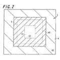
- the optical apparatus 1 is seen through from above, as indicated by the broken line in Fig. 1A , the element substrate 3 is positioned inside the wiring board 4. In this case, the external connection terminals 8 are positioned around the element substrate 3.
- the broken line B in Fig. 1A indicates a boundary between an area A2 that includes the sealing member 5 and an area A3 that includes the external connection terminals 8.
- an insulating substrate 10 that contains the wiring conductor 7 and a light-transmitting substrate 11 that transmits desired light are bonded to each other.
- the light-transmitting substrate 11 is a glass substrate.
- the glass substrate 11 is laminated on the insulating substrate 10.
- the insulating substrate 10 is, for example, a laminate in which a plurality of insulating layers made of glass ceramics are laminated one on top of another.
- the insulating substrate 10 faces the element substrate 3.
- the insulating substrate 10 has a through-hole 12 in an area that faces the optical MEMS 2.
- the optical MEMS 2 can receive light that has been transmitted through the glass substrate 11 and has passed through the through-hole 12.
- the optical MEMS 2 is a so-called DMD (digital micromirror device)
- light that has transmitted through the glass substrate 11 is scanned by the optical MEMS 2.
- the surface S of the wiring board 4 is stepped. That is to say, as shown in Fig. 2 , the surface S has a plurality of areas A1 to A3 with different distances from the glass substrate 11. For example, in the first area A1 that faces the optical MEMS 2, a distance H1 from the glass substrate 11 is 0. In the second area A2 that is positioned around the first area A1, a distance H2 from the glass substrate 11 is longer than the distance H1. This second area A2 includes the sealing member 5 and the conductive members 6. Furthermore, in the third area A3 that is positioned around the second area A2 and that includes the external connection terminals 8, a distance H3 from the glass substrate 11 is shorter than the distance H2. In the case where the distance H3 is shorter than the distance H2 in this manner, projection of the external connection terminals 8 outside of the optical apparatus 1 can be suppressed. As a result, the size of the optical apparatus 1 can be reduced.
- the insulating substrate 10 and the glass substrate 11 may be integrated by sintering. More specifically, the insulating substrate 10 may be bonded to the glass substrate 11, by bringing a glass-ceramic green sheet into close contact with the glass substrate 11 by thermocompression bonding, and sintering the glass-ceramic green sheet so as to be integrated with the glass substrate 11.
- the glass-ceramic green sheet is obtained by forming a raw powder for the insulating substrate 10, such as a glass powder, a ceramic powder, or the like, into a sheet. At that time, the insulating substrate 10 is bonded to the glass substrate 11, due to a glass component in the insulating substrate 10.
- a raw powder for the insulating substrate 10 such as a glass powder, a ceramic powder, or the like
- the glass substrate 11 and the insulating substrate 10 can be brought into closer contact with each other, and the airtightness of the optical apparatus 1 can be improved.
- the glass substrate 11 is required not to be melted and softened at a sintering temperature (800 to 950°C) of the insulating substrate 10, and not to be opacified by internally precipitating crystals, in order to function as an optical path.
- the glass substrate 11 is preferably made of silica glass or glass derived therefrom.
- silica glass is more preferable because this material has a coefficient of thermal expansion close to that of a semiconductor substrate, has heat resistance to the firing temperature of glass ceramics, and is hard to be opacified by crystallization of glass.
- the thickness of the glass substrate 11 in this example, the thickness of the glass substrate 11 in the laminating direction of the glass substrate 11 and the insulating substrate 10 is 0.1 to 0.5 mm.
- the thickness of the glass substrate 11 is 0.1 mm or more, the strength of the glass substrate 11 can be assured, and breakage of the glass substrate 11 during thermocompression bonding of the glass-ceramic green sheet and the glass substrate 11 can be suppressed.
- the thickness of the glass substrate 11 is 0.5 mm or less, a loss of transmitted light due to the glass substrate 11 can be suppressed, and, thus, the properties of the optical MEMS 2 can be improved.
- the degree of freedom in arrangement of the wiring conductor 7 in the insulating substrate 10 is increased, and the degree of freedom in electric connection between the wiring board 4 and the element substrate 3, and between the wiring board 4 and an external circuit board can be increased.
- the wiring conductor 7 may be formed by co-firing with a glass-ceramic green sheet forming the insulating substrate 10.
- a hole is formed through a glass-ceramic green sheet using punching, laser beam machining or other methods, and, then, is filled with a conductor paste obtained by forming a metal powder of Ag, Cu, or the like into a paste.
- the conductor paste is applied to the glass-ceramic green sheet by screen printing or other methods.
- a plurality of such ceramic green sheets having a surface and a hole to which the conductor paste is applied are laminated and fired, and, thus, a multi-layered wiring structure can be formed.
- the wiring conductor 7 is formed in the ceramic substrate by co-firing in this manner, the wiring conductor 7 is brought into close contact with the insulating substrate 10 in a preferable manner. Accordingly, formation of a gap between the wiring conductor 7 and the insulating substrate 10 can be suppressed, and, thus, the airtight reliability of the optical apparatus 1 can be increased.
- the wiring conductor 7 formed by co-firing as described above can be formed to a thickness of approximately 10 to 30 ⁇ m, and, thus, the resistance of the wiring conductor 7 can be reduced.
- the wiring layer of the glass substrate 11 and the wiring conductor 7 can be bonded to each other to obtain conduction, by firing the wiring layer of the glass substrate 11 and the conductor paste of the insulating substrate 10 in a contact state. Accordingly, the wiring conductor 7 inside the insulating substrate 10 and the wiring layer on the glass substrate 11 can be electrically connected to each other, and, thus, the degree of freedom in electric connection can be increased.
- the external connection terminals 8 can be arranged on the surface of the glass substrate 11 without being connected to the surface S.
- the wiring conductor 7 is formed, for example, by sintering a metal powder of Ag, Cu, or Au, or an alloy thereof.
- the insulating substrate 10 is made of a crystallized material having a coefficient of thermal expansion close to that of the glass substrate 11.
- the insulating substrate 10 has a coefficient of thermal expansion of 1.5 to 3.0 ⁇ 10 -6 /°C, which is close to the coefficient of thermal expansion of silica glass, and a degree of crystallization of 70% or more.
- the glass-ceramic sintered compact is hard to be damaged in a step of washing the glass substrate 11, and, thus, shedding of particles from the glass-ceramic sintered compact can be reduced.
- the insulating substrate 10 having a low coefficient of thermal expansion and a high degree of crystallization can be made of a glass material in which cordierite, ⁇ -quartz, ⁇ -spodumene, or ⁇ -eucryptite is precipitated in the crystal phase, and the crystals or a solid solution thereof can be added to this crystal layer as fillers in order to adjust the coefficient of thermal expansion.
- the wiring conductor 7 is disposed in at least one of the internal portion and the surface portion of the insulating substrate 10. In the case where the wiring conductor 7 has a multi-layered wiring structure, the degree of freedom in design of the optical apparatus 1 can be increased.
- the semiconductor substrate 3 functions as a spacer during secondary mounting. With this spacer, the height of the external connection terminals 8 can be maintained. Thus, even in the case where the wiring board 4 and an external circuit board have mutually different coefficients of thermal expansion, the reliability of the optical apparatus 1 mounted on an external circuit board can be improved.
- the conductive members 6 can be made of, for example, a metal material, such as Au, Ag, Cu, Ni, or the like, or an alloy material thereof.
- a metal material such as Au, Ag, Cu, Ni, or the like
- the conductive members 6 may be formed by A stud bumping.
- the external connection terminals 8 are ordinarily made of a solder material, such as Pb-Sn, SnAg, SnAgCu, or the like.
- the external connection terminals 8 are made of, for example, SnAgCu solder internally containing metal balls, in order to relax a thermal stress between the optical apparatus 1 and the external circuit board.
- the sealing member 5 is made of a material that has heat resistance during secondary mounting of the optical apparatus 1. It is desirable that this sort of sealing member 5 is made of, for example, Pb-Sn, AuSn, or fritted glass, in particular, AuSn or fritted glass material. These materials melt and flow at 300 to 450°C, and, thus, a sealing member 5 having smaller gaps and a small void ratio can be formed.
- a method of manufacturing the optical apparatus 1 will be described.
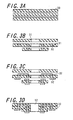
- the glass-ceramic green sheets 30 are prepared as follows: a glass powder, a ceramic powder, an organic binder, an organic solvent, a plasticizer, and the like are combined and mixed to form a slurry, and this slurry is formed into sheets using the doctor blade method or the calender roll method.
- the ceramic powder is, for example, crystals of cordierite, ⁇ -quart, ⁇ -spodumene, ⁇ -eucryptite, or the like, or a solid solution powder thereof.
- the glass powder is, for example, an SiO 2 -B 2 O 3 -based powder, an SiO 2 -B 2 O 3 -Al 2 O 3 -based powder, or an SiO 2 -B 2 O 3 -AlO 3 -MgO-based powder.
- Examples of a combination of the ceramic powder and the glass powder include a combination in which the ceramic powder is cordierite and the glass powder is crystallized glass in which 70% or more of the cordierite is precipitated.
- the obtained glass-ceramic sintered compact has a coefficient of thermal expansion of 2.0 to 3.0 ⁇ 10 -6 /°C, and a degree of crystallization of 70% to 80% or more, and, thus, this combination is more preferable.
- organic binder those conventionally used for ceramic green sheets can be used, and examples thereof include acrylic-based, polyvinyl butyral-based, polyvinyl alcohol-based, polypropylene carbonate-based, and cellulose-based homopolymers and copolymers.
- the organic solvent used in the slurry for forming the green sheets is made of, for example, hydrocarbons, ethers, esters, ketones, alcohols, or the like, in order to obtain a slurry having an appropriate viscosity for forming green sheets by kneading the organic solvent, the glass powder, the ceramic powder, and the organic binder.
- the glass-ceramic green sheets 30 produced in Fig. 3A are subjected to mechanical processing, such as die machining, laser beam machining, microdrilling, punching, or the like, and, thus, through-holes 31 are formed.
- These through-holes 31 are used as through-holes for vias, or used for forming the through-hole 12 that accommodates the optical MEMS 2.
- the through-holes for vias are filled with a conductor paste 32 in which an appropriate organic binder and solvent are added to and mixed with a metal powder of, for example, Ag, Cu, Ag-Pt, Ag-Pd, or the like, and a glass powder, using screen printing or other methods.
- the conductor paste 32 is applied to the surfaces of the glass-ceramic green sheets 30 by screen printing or the like.
- the glass-ceramic green sheets 30 to which the conductor paste 32 has been applied are subjected to thermocompression bonding under a pressure of 3 to 20 MPa and a temperature of 50 to 80°C, and, thus, a green sheet laminate 33 is formed.
- a glass-ceramic green sheet 30 disposed as an uppermost layer of the green sheet laminate 33 contains a melting component that melts due to heat applied for close contact.
- the glass substrate 11 and the green sheet laminate 33 are subjected to thermocompression bonding under a pressure of 3 to 10 MPa and a temperature of 50 to 80°C, and, thus, the glass substrate 11 and the green sheet laminate 33 are thermocompression bonded to each other.
- an outermost layer of the green sheet laminate 33 that is, a glass-ceramic green sheet 30 brought into contact with the glass substrate 11 contains a melting component that melts due to heat applied for close contact.
- the glass substrate 11 and the green sheet laminate 33 can be brought into close contact with each other under a lower pressure, and, thus, the possibility of breaking the glass substrate 11 can be reduced in the step of Fig. 3E .
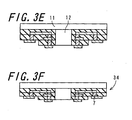
- the green sheet laminate 33 that has been thermocompression bonded to the glass substrate 11 is fired, and, thus, a composite substrate 34 (the wiring board 4) is formed.
- the wiring conductor 7 is made of a sintered compact of, for example, an Ag, Ag-Pt, or Ag-Pd metal powder
- the firing is performed in air at a temperature of 800 to 1000°C.
- the wiring conductor 7 is made of a sintered compact of a Cu metal powder
- the firing is performed in a nitrogen atmosphere.
- a composite substrate 34 can be obtained in which positional displacement can be reduced between an electrode on the element substrate 3 and a conductive pad, which is part of the wiring conductor 7 formed in the green sheet laminate 33.
- a semiconductor substrate 3 is prepared.
- the semiconductor substrate 3 is made of single crystal or multicrystal silicon.
- the optical MEMS 2 is formed on the surface of the semiconductor substrate 3 using a micromachining technique.
- the semiconductor substrate 3 and the composite substrate 34 are connected to each other via the sealing member 5 and the conductive members 6 such that the optical MEMS 2 and the through-hole 12 of the composite substrate 34 face each other.
- the sealing member 5 and the conductive members 6 may be bonded in advance to a surface of either the semiconductor substrate 3 or the composite substrate 34.
- the semiconductor substrate 3 and the composite substrate 34 are connected to each other under the condition of a temperature of 300 to 450°C and a pressure of several megapascals (MPa) to several tens of megapascals (MPa).
- the temperature applied during the connection is a temperature higher than the melting points of the sealing material forming the sealing member 5, and the conductive members.
- a pressure is applied in order to correct warping of the semiconductor substrate 3 and the composite substrate 34.
- the conductive members 6 are made of Au bumps
- the sealing material forming the sealing member 5 is made of AuSn solder or fritted glass.
- the Au bumps can be formed using a known stud bump method with Au wires, and the sealing member 5 can be formed by applying a paste using a screen printing method and causing the paste to melt them by reflow processing or the like. With the Au bumps, the distance can be easily controlled between the semiconductor substrate 3 and the composite substrate 34.
- the sealing material made of AuSn solder or fritted glass forms a liquid phase, and can flow to fill small gaps, and, thus, a sealing member 5 having a high reliability can be formed.
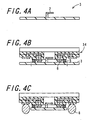
- the semiconductor substrate 3 is cut at a position indicated by the broken lines in Fig. 4B , and a peripheral portion of the semiconductor substrate 3 is removed.
- solder balls are attached as the external connection terminals 8 to a peripheral portion of the surface of the wiring board 4, using appropriate jigs and tools.
- the optical apparatus 1 can sufficiently transmit light to the optical MEMS, and can secure electric connection having a high reliability between the optical MEMS and an external circuit. Furthermore, in the optical apparatus 1, the insulating substrate 10 made of glass ceramics and the semiconductor substrate 3 are connected to each other via the sealing member 5, and, thus, the optical MEMS 2 can be hermetically sealed. In particular, since the glass substrate 11 and the insulating substrate 10 are integrated by sintering, and, thus, close contact between the insulating substrate 10 and the glass substrate 11 can be maintained in a preferable manner, and the airtightness of the optical MEMS 2 can be improved.
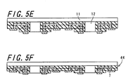
- Figs. 5A to 6C correspond to Figs. 3A to 4C , and the same configurations are denoted by the same reference numerals. In this example, only main points of difference from Figs. 3A to 4C will be described. That is to say, description of configurations as in Figs. 3A to 4C may be omitted.
- glass-ceramic green sheets 40 are prepared.
- through-holes 31 used as through-holes for vias, or used for forming the through-holes 12 that accommodate the optical MEMSs 2 are formed through the glass-ceramic green sheets 40 formed in Fig. 5A .
- the through-holes for vias are filled with a conductor paste 32 using screen printing or other methods.
- the conductor paste 32 is applied to the surfaces of the glass-ceramic green sheets 40.
- the glass-ceramic green sheets 40 to which the conductor paste 32 has been applied are subjected to thermocompression bonding under a pressure of 3 to 20 MPa and a temperature of 50 to 80°C, and, thus, a green sheet laminate 43 is formed.
- the glass substrate 11 and the green sheet laminate 43 are subjected to thermocompression bonding under the condition of a pressure of 3 to 10 MPa and a temperature of 50 to 80°C, and, thus, the glass substrate 11 and the green sheet laminate 43 are thermocompression bonded to each other.
- the green sheet laminate 43 that has been thermocompression bonded to the glass substrate 11 is fired, and, thus, a composite base substrate 44 is formed.
- a semiconductor base substrate 45 is prepared.
- a plurality of optical MEMSs 2 are arranged in a matrix on a 4 to 8-inch silicon wafer using a micromachining technique.
- the composite base substrate 44 and the semiconductor base substrate 45 are connected to each other at the wafer level, and, thus, electric connection between the substrates 44 and 45 and hermetic sealing of the optical MEMS 2 are simultaneously obtained.
- the composite base substrate 44 and the semiconductor base substrate 45 are connected to each other at the wafer level at a temperature of 300 to 450°C, which is higher than the melting points of the sealing material forming the sealing member 5, and the conductive members 6, and under a pressure of several megapascals (MPa) to several tens of megapascals (MPa) in order to correct warping of the members.
- the composite base substrate 44 and the semiconductor base substrate 45 are separated into pieces using dicing or the like, and, thus, a plurality of optical apparatuses 1 can be formed.
- the surface of the wiring board 4 is stepped such that the distance H3 from the glass substrate 11 to the third area A3 that is to be connected to the external connection terminals 8 is shorter than the distance H2 from the glass substrate 11 to the second area A2 by 0.1 mm or more. Since the distance H3 is shorter than the distance H2 by 0.1 mm or more, damage on the third area A3 caused by a dicing blade can be suppressed in the separating step using dicing.
- solder balls are attached as the external connection terminals 8 to peripheral portions of the surfaces of the wiring boards 4, using appropriate jigs and tools.
- the wiring board 3 functions as a cover that covers the optical MEMS 2. Accordingly, an optical apparatus that can transmit light to the optical MEMS 2 and that can realize electric connection having a high degree of freedom between the optical MEMS 2 and an external circuit can be more easily formed at the wafer level.
- Examples of the optical MEMS 2 described above include a micromirror device that controls a reflection direction by tilting a micromirror using an electrostatic force, a grating light valve device that controls a diffraction direction using the movement of a small diffraction element, and the like.
- an optical MEMS formed on a surface of a substrate using a micromachining technique is shown as an example of an optical element, but a separately formed optical element may be provided on the substrate.
- the optical element 2 may be, for example, a light modulation element.
- the external connection terminals 8 are realized as solder balls, but there is no limitation to this.
- the external connection terminals 8 may be realized through attachment of various pins.
Landscapes
- Engineering & Computer Science (AREA)
- Microelectronics & Electronic Packaging (AREA)
- Manufacturing & Machinery (AREA)
- Computer Hardware Design (AREA)
- Micromachines (AREA)
- Mechanical Light Control Or Optical Switches (AREA)
- Light Receiving Elements (AREA)
- Led Device Packages (AREA)
Applications Claiming Priority (2)
| Application Number | Priority Date | Filing Date | Title |
|---|---|---|---|
| JP2007308274 | 2007-11-29 | ||
| PCT/JP2008/071829 WO2009069807A1 (ja) | 2007-11-29 | 2008-12-01 | 光学装置、封止用基板および光学装置の製造方法 |
Publications (2)
| Publication Number | Publication Date |
|---|---|
| EP2239619A1 true EP2239619A1 (de) | 2010-10-13 |
| EP2239619A4 EP2239619A4 (de) | 2013-04-24 |
Family
ID=40678694
Family Applications (1)
| Application Number | Title | Priority Date | Filing Date |
|---|---|---|---|
| EP08853336.9A Withdrawn EP2239619A4 (de) | 2007-11-29 | 2008-12-01 | Optische anordnung, dichtplatte und verfahren zur herstellung einer optischen anordnung |
Country Status (4)
| Country | Link |
|---|---|
| US (1) | US8204352B2 (de) |
| EP (1) | EP2239619A4 (de) |
| JP (2) | JP5349024B2 (de) |
| WO (1) | WO2009069807A1 (de) |
Families Citing this family (2)
| Publication number | Priority date | Publication date | Assignee | Title |
|---|---|---|---|---|
| DE102013217146A1 (de) * | 2013-08-28 | 2015-03-05 | Carl Zeiss Smt Gmbh | Optisches Bauelement |
| JP6279857B2 (ja) * | 2013-08-29 | 2018-02-14 | 京セラ株式会社 | 電子装置、多数個取り枠体および多数個取り電子装置 |
Family Cites Families (15)
| Publication number | Priority date | Publication date | Assignee | Title |
|---|---|---|---|---|
| JP3207319B2 (ja) * | 1993-05-28 | 2001-09-10 | 株式会社東芝 | 光電変換装置及びその製造方法 |
| EP0630056B1 (de) * | 1993-05-28 | 1998-02-18 | Toshiba Ave Co., Ltd | Verwendung einer anisotropischen leitfähigen Schicht für die Verbindung von Anschlussleitern einer Leiterplatte mit den elektrischen Anschlusskontakten einer photoelektrischen Umwandlungsvorrichtung und Verfahren zur Montage dieser Vorrichtung |
| US6507082B2 (en) * | 2000-02-22 | 2003-01-14 | Texas Instruments Incorporated | Flip-chip assembly of protected micromechanical devices |
| US6661084B1 (en) * | 2000-05-16 | 2003-12-09 | Sandia Corporation | Single level microelectronic device package with an integral window |
| JP2002076313A (ja) * | 2000-08-28 | 2002-03-15 | Canon Inc | 固体撮像装置 |
| JP2002141430A (ja) | 2000-10-31 | 2002-05-17 | Kyocera Corp | デジタルマイクロミラーデバイス収納用パッケージ |
| JP4342174B2 (ja) * | 2002-12-27 | 2009-10-14 | 新光電気工業株式会社 | 電子デバイス及びその製造方法 |
| JP4505189B2 (ja) * | 2003-03-24 | 2010-07-21 | 富士フイルム株式会社 | 透過型光変調装置及びその実装方法 |
| US20040232535A1 (en) * | 2003-05-22 | 2004-11-25 | Terry Tarn | Microelectromechanical device packages with integral heaters |
| JP4170950B2 (ja) * | 2003-10-10 | 2008-10-22 | 松下電器産業株式会社 | 光学デバイスおよびその製造方法 |
| JP4686134B2 (ja) * | 2004-04-26 | 2011-05-18 | パナソニック株式会社 | 光学デバイスおよびその製造方法 |
| KR100815350B1 (ko) * | 2005-04-01 | 2008-03-19 | 삼성전기주식회사 | 광변조기 모듈 패키지 구조 |
| JP2006301153A (ja) * | 2005-04-19 | 2006-11-02 | Sony Corp | 回折格子−光変調装置組立体 |
| KR100995301B1 (ko) * | 2005-12-26 | 2010-11-19 | 쿄세라 코포레이션 | 마이크로 전자 기계 장치 및 그 제조방법 |
| US8138588B2 (en) * | 2006-12-21 | 2012-03-20 | Texas Instruments Incorporated | Package stiffener and a packaged device using the same |
-
2008
- 2008-12-01 EP EP08853336.9A patent/EP2239619A4/de not_active Withdrawn
- 2008-12-01 US US12/745,634 patent/US8204352B2/en not_active Expired - Fee Related
- 2008-12-01 JP JP2008305984A patent/JP5349024B2/ja not_active Expired - Fee Related
- 2008-12-01 WO PCT/JP2008/071829 patent/WO2009069807A1/ja not_active Ceased
- 2008-12-01 JP JP2009543901A patent/JP5292307B2/ja not_active Expired - Fee Related
Also Published As
| Publication number | Publication date |
|---|---|
| JPWO2009069807A1 (ja) | 2011-04-21 |
| WO2009069807A1 (ja) | 2009-06-04 |
| US20100310216A1 (en) | 2010-12-09 |
| JP2009151297A (ja) | 2009-07-09 |
| US8204352B2 (en) | 2012-06-19 |
| EP2239619A4 (de) | 2013-04-24 |
| JP5292307B2 (ja) | 2013-09-18 |
| JP5349024B2 (ja) | 2013-11-20 |
Similar Documents
| Publication | Publication Date | Title |
|---|---|---|
| JP4938779B2 (ja) | 微小電子機械機構装置およびその製造方法 | |
| EP2121511B1 (de) | Verpackungsverfahren eines elektronischen oder micromechanischen bauteils | |
| US7932594B2 (en) | Electronic component sealing substrate for hermetically sealing a micro electronic mechanical system of an electronic component | |
| WO2008066087A1 (en) | Fine structure device, method for manufacturing the fine structure device and substrate for sealing | |
| JP4741621B2 (ja) | 電子部品封止用基板およびそれを用いた電子装置、並びに電子装置の製造方法 | |
| JPWO2007074846A1 (ja) | 微小電子機械装置およびその製造方法ならびに配線基板 | |
| JP4268480B2 (ja) | 電子部品封止用基板およびそれを用いた電子装置 | |
| JP2005262382A (ja) | 電子装置およびその製造方法 | |
| US8204352B2 (en) | Optical apparatus, sealing substrate, and method of manufacturing optical apparatus | |
| JP3842751B2 (ja) | 電子部品封止用基板およびそれを用いた電子装置の製造方法 | |
| JP4761713B2 (ja) | 電子部品封止用基板および多数個取り用電子部品封止用基板ならびに電子装置の製造方法 | |
| JP4126459B2 (ja) | 電子部品封止用基板およびそれを用いた電子装置、並びに電子装置の製造方法 | |
| JP5013824B2 (ja) | 電子部品封止用基板および複数個取り形態の電子部品封止用基板、並びに電子部品封止用基板を用いた電子装置および電子装置の製造方法 | |
| JP4903540B2 (ja) | 微小電子機械部品封止用基板及び複数個取り形態の微小電子機械部品封止用基板、並びに微小電子機械装置及び微小電子機械装置の製造方法 | |
| JP4116954B2 (ja) | 電子部品封止用基板およびそれを用いた電子装置 | |
| JP2005212016A (ja) | 電子部品封止用基板および多数個取り用電子部品封止用基板ならびに電子装置の製造方法 | |
| JP4434870B2 (ja) | 多数個取り電子部品封止用基板および電子装置ならびに電子装置の製造方法 | |
| JP4731291B2 (ja) | 電子部品封止用基板およびそれを用いた電子装置、電子装置の製造方法 | |
| JP4781098B2 (ja) | 電子装置 | |
| JP4404647B2 (ja) | 電子装置および電子部品封止用基板 | |
| JP2005153067A (ja) | 電子部品封止用基板およびそれを用いた電子装置の製造方法 | |
| JP2006295213A (ja) | 電子部品封止用基板および多数個取り形態の電子部品封止用基板、並びに電子装置 | |
| JP2007013017A (ja) | 電子デバイス装置およびその製造方法 | |
| JP2009289952A (ja) | 機能デバイス及び機能デバイスの製造方法 |
Legal Events
| Date | Code | Title | Description |
|---|---|---|---|
| PUAI | Public reference made under article 153(3) epc to a published international application that has entered the european phase |
Free format text: ORIGINAL CODE: 0009012 |
|
| 17P | Request for examination filed |
Effective date: 20100629 |
|
| AK | Designated contracting states |
Kind code of ref document: A1 Designated state(s): AT BE BG CH CY CZ DE DK EE ES FI FR GB GR HR HU IE IS IT LI LT LU LV MC MT NL NO PL PT RO SE SI SK TR |
|
| AX | Request for extension of the european patent |
Extension state: AL BA MK RS |
|
| DAX | Request for extension of the european patent (deleted) | ||
| A4 | Supplementary search report drawn up and despatched |
Effective date: 20130326 |
|
| RIC1 | Information provided on ipc code assigned before grant |
Ipc: G02B 26/08 20060101ALI20130320BHEP Ipc: H05K 1/18 20060101ALI20130320BHEP Ipc: B81B 7/00 20060101ALI20130320BHEP Ipc: G02F 1/01 20060101AFI20130320BHEP Ipc: H01L 23/02 20060101ALI20130320BHEP Ipc: B81C 1/00 20060101ALI20130320BHEP |
|
| STAA | Information on the status of an ep patent application or granted ep patent |
Free format text: STATUS: THE APPLICATION HAS BEEN WITHDRAWN |
|
| 18W | Application withdrawn |
Effective date: 20131002 |