EP2235743B1 - Zweidimensionale strukturierung unter verwendung eines selbstassemblierten materials - Google Patents
Zweidimensionale strukturierung unter verwendung eines selbstassemblierten materials Download PDFInfo
- Publication number
- EP2235743B1 EP2235743B1 EP09704665.0A EP09704665A EP2235743B1 EP 2235743 B1 EP2235743 B1 EP 2235743B1 EP 09704665 A EP09704665 A EP 09704665A EP 2235743 B1 EP2235743 B1 EP 2235743B1
- Authority
- EP
- European Patent Office
- Prior art keywords
- layer
- line
- nanoscale
- self
- forming
- Prior art date
- Legal status (The legal status is an assumption and is not a legal conclusion. Google has not performed a legal analysis and makes no representation as to the accuracy of the status listed.)
- Not-in-force
Links
Images


Classifications
-
- H—ELECTRICITY
- H01—ELECTRIC ELEMENTS
- H01L—SEMICONDUCTOR DEVICES NOT COVERED BY CLASS H10
- H01L21/00—Processes or apparatus adapted for the manufacture or treatment of semiconductor or solid state devices or of parts thereof
- H01L21/02—Manufacture or treatment of semiconductor devices or of parts thereof
- H01L21/027—Making masks on semiconductor bodies for further photolithographic processing not provided for in group H01L21/18 or H01L21/34
- H01L21/033—Making masks on semiconductor bodies for further photolithographic processing not provided for in group H01L21/18 or H01L21/34 comprising inorganic layers
- H01L21/0334—Making masks on semiconductor bodies for further photolithographic processing not provided for in group H01L21/18 or H01L21/34 comprising inorganic layers characterised by their size, orientation, disposition, behaviour, shape, in horizontal or vertical plane
- H01L21/0337—Making masks on semiconductor bodies for further photolithographic processing not provided for in group H01L21/18 or H01L21/34 comprising inorganic layers characterised by their size, orientation, disposition, behaviour, shape, in horizontal or vertical plane characterised by the process involved to create the mask, e.g. lift-off masks, sidewalls, or to modify the mask, e.g. pre-treatment, post-treatment
-
- B—PERFORMING OPERATIONS; TRANSPORTING
- B81—MICROSTRUCTURAL TECHNOLOGY
- B81C—PROCESSES OR APPARATUS SPECIALLY ADAPTED FOR THE MANUFACTURE OR TREATMENT OF MICROSTRUCTURAL DEVICES OR SYSTEMS
- B81C1/00—Manufacture or treatment of devices or systems in or on a substrate
- B81C1/00015—Manufacture or treatment of devices or systems in or on a substrate for manufacturing microsystems
- B81C1/00023—Manufacture or treatment of devices or systems in or on a substrate for manufacturing microsystems without movable or flexible elements
- B81C1/00031—Regular or irregular arrays of nanoscale structures, e.g. etch mask layer
-
- B—PERFORMING OPERATIONS; TRANSPORTING
- B82—NANOTECHNOLOGY
- B82Y—SPECIFIC USES OR APPLICATIONS OF NANOSTRUCTURES; MEASUREMENT OR ANALYSIS OF NANOSTRUCTURES; MANUFACTURE OR TREATMENT OF NANOSTRUCTURES
- B82Y10/00—Nanotechnology for information processing, storage or transmission, e.g. quantum computing or single electron logic
-
- B—PERFORMING OPERATIONS; TRANSPORTING
- B82—NANOTECHNOLOGY
- B82Y—SPECIFIC USES OR APPLICATIONS OF NANOSTRUCTURES; MEASUREMENT OR ANALYSIS OF NANOSTRUCTURES; MANUFACTURE OR TREATMENT OF NANOSTRUCTURES
- B82Y30/00—Nanotechnology for materials or surface science, e.g. nanocomposites
-
- H—ELECTRICITY
- H01—ELECTRIC ELEMENTS
- H01L—SEMICONDUCTOR DEVICES NOT COVERED BY CLASS H10
- H01L21/00—Processes or apparatus adapted for the manufacture or treatment of semiconductor or solid state devices or of parts thereof
- H01L21/02—Manufacture or treatment of semiconductor devices or of parts thereof
- H01L21/027—Making masks on semiconductor bodies for further photolithographic processing not provided for in group H01L21/18 or H01L21/34
- H01L21/033—Making masks on semiconductor bodies for further photolithographic processing not provided for in group H01L21/18 or H01L21/34 comprising inorganic layers
- H01L21/0334—Making masks on semiconductor bodies for further photolithographic processing not provided for in group H01L21/18 or H01L21/34 comprising inorganic layers characterised by their size, orientation, disposition, behaviour, shape, in horizontal or vertical plane
- H01L21/0338—Process specially adapted to improve the resolution of the mask
-
- B—PERFORMING OPERATIONS; TRANSPORTING
- B81—MICROSTRUCTURAL TECHNOLOGY
- B81C—PROCESSES OR APPARATUS SPECIALLY ADAPTED FOR THE MANUFACTURE OR TREATMENT OF MICROSTRUCTURAL DEVICES OR SYSTEMS
- B81C2201/00—Manufacture or treatment of microstructural devices or systems
- B81C2201/01—Manufacture or treatment of microstructural devices or systems in or on a substrate
- B81C2201/0101—Shaping material; Structuring the bulk substrate or layers on the substrate; Film patterning
- B81C2201/0147—Film patterning
- B81C2201/0149—Forming nanoscale microstructures using auto-arranging or self-assembling material
-
- Y—GENERAL TAGGING OF NEW TECHNOLOGICAL DEVELOPMENTS; GENERAL TAGGING OF CROSS-SECTIONAL TECHNOLOGIES SPANNING OVER SEVERAL SECTIONS OF THE IPC; TECHNICAL SUBJECTS COVERED BY FORMER USPC CROSS-REFERENCE ART COLLECTIONS [XRACs] AND DIGESTS
- Y10—TECHNICAL SUBJECTS COVERED BY FORMER USPC
- Y10T—TECHNICAL SUBJECTS COVERED BY FORMER US CLASSIFICATION
- Y10T428/00—Stock material or miscellaneous articles
- Y10T428/24—Structurally defined web or sheet [e.g., overall dimension, etc.]
- Y10T428/24479—Structurally defined web or sheet [e.g., overall dimension, etc.] including variation in thickness
- Y10T428/24612—Composite web or sheet
Definitions
- the present invention relates generally to nanoscale structures, and more particularly to two-dimensional self-assembled sublithographic nanoscale structures in a regular periodic array and methods for manufacturing the same.
- bottom-up approaches to semiconductor fabrication has grown in interest within the semiconductor industry.
- One such approach utilizes self-assembling block copolymers for generation of sublithographic ground rule nanometer scale patterns.
- Self-assembling copolymer materials that are capable of self-organizing into nanometer-scale patterns may be applied within a recessed region of a template layer to form a nanoscale structure.
- the two or more immiscible polymeric block components separate into two or more different phases on a nanometer scale, and thereby form ordered patterns of isolated nano-sized structural units.
- ordered patterns of isolated nano-sized structural units formed by the self-assembling block copolymers can be used for fabricating nano-scale structural units in semiconductor, optical, and magnetic devices. Dimensions of the structural units so formed are typically in the range of 5 to 40 nm, which are sublithographic (i.e., below the resolution of the lithographic tools).
- the self-assembling block copolymers are first dissolved in a suitable solvent system to form a block copolymer solution, which is then applied onto the surface of an underlayer to form a block copolymer layer.
- the self-assembling block copolymers are annealed at an elevated temperature to form two sets of polymer block structures containing two different polymeric block components.
- the polymeric block structure may be lines or cylinders.
- One set of polymer block structures may be embedded in the other set of polymer block structures, or polymeric block structures belonging to different sets may alternate.
- the self-assembling block copolymers are non-photosensitive resists, of which the patterning is effected not by photons, i.e., optical radiation, but by self-assembly under suitable conditions such as an anneal.
- US Patent No. 5,916,821 discloses a method for producing sublithographic etching masks.
- the present invention addresses the needs described above by providing a rectangular array of nanoscale structures having sublithographic width and spacing in two different directions, and methods of manufacturing the same.
- a first nanoscale self-aligned self-assembled nested line structure having a sublithographic width and a sublithographic spacing and running along a first direction is formed from first self-assembling block copolymers within a first layer.
- the first layer is filled with a filler material and a second layer is deposited above the first layer containing the first nanoscale nested line structure.
- a second nanoscale self-aligned self-assembled nested line structure having a sublithographic width and a sublithographic spacing and running in a second direction is formed from second self-assembling block copolymers within the second layer.
- the second direction is different from the first direction, and may or may not be orthogonal to the first direction.
- the composite pattern of the first nanoscale nested line structure and the second nanoscale nested line structure is transferred into an underlayer beneath the first layer to form an array of structures containing periodicity in two directions.
- the present invention provides a method as claimed in claim 1.
- the first nanoscale self-assembled self-aligned structure is located at or beneath a top surface of the first layer.
- the first nanoscale self-assembled self-aligned structure is located at or beneath a top surface of the second layer.
- the method comprises applying a first non-photosensitive polymeric resist comprising a first polymeric component and a second polymeric component in the first recessed region, wherein the at least one first line comprises the first polymeric component.
- the method further comprises: forming at least one third line having a third sublithographic width, comprising the second polymeric component, and laterally abutting the at least one first line in the first recessed region; and removing the at least one third line selective to the at least one first line and the first layer.
- the method further comprises filling a space formed by removal of the at least one third line with a filler material that is different from the first non-photosensitive polymeric resist.
- the method further comprises applying a second non-photosensitive polymeric resist comprising a third polymeric component and a fourth polymeric component in the second recessed region, wherein the at least one second line comprises the third polymeric component.
- the method further comprises: forming at least one fourth line having a fourth sublithographic width, comprising the fourth polymeric component, and laterally abutting the at least one second line in the second recessed region; and removing the at least one fourth line selective to the at least one second line and the second layer.
- the at least one first line comprises a polymeric component of a first non-photosensitive polymeric resist and the at least one second line comprises a polymeric component of a second non-photosensitive polymeric resist, and the method further comprises removing the second layer selective to the at least one second line.
- the method further comprises removing the first layer selective to the at least one first line and the at least one second line.
- the method further comprises forming a structure comprising a two dimensional array of nanoscale trenches in an underlayer beneath the first layer and on the substrate, wherein the nanoscale trenches are repeated along a first direction and a second direction within the two dimensional array, and wherein each of the nanoscale trenches has a first pair of sidewalls separated by a first sublithographic distance and a second pair of sidewalls separated by a second sublithographic distance.
- first direction is perpendicular to the two parallel first lengthwise edges
- second direction is perpendicular to the two parallel second lengthwise edges
- a horizontal cross-sectional area of the nanoscale trenches is a parallelogram.
- the horizontal cross-sectional area of the nanoscale trenches is a rectangle.
- the present invention relates to two-dimensional self-assembled sublithographic nanoscale structures in a regular periodic array and methods for manufacturing for the same, which are now described in detail with accompanying figures. It is noted that like and corresponding elements are referred to by like reference numerals.
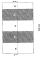
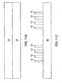
- a first exemplary nanoscale structure according to a first embodiment of the present invention comprises an underlayer 12 located on a substrate 10 and a first layer 20.
- the substrate 10 may be a semiconductor substrate, an insulator substrate, a metallic substrate, or a combination thereof.
- the semiconductor substrate may be a silicon substrate, other group IV element semiconductor substrate, or a compound semiconductor substrate.
- the semiconductor substrate may be a bulk substrate, a semiconductor-on-insulator (SOI) substrate, or a hybrid substrate having a bulk portion and an SOI portion.
- SOI semiconductor-on-insulator
- the underlayer 12 may comprise a semiconductor material, an insulator material, or a metal.
- Exemplary material for the semiconductor material comprises group IV elements as a pure material or as an alloy, III-V compound semiconductor materials, and II-VI compound semiconductor materials.
- the semiconductor material may be doped with dopants, or may be substantially undoped.
- Exemplary insulator materials include a dielectric oxide, a dielectric nitride, and a porous or non-porous low-dielectric constant dielectric material (having a dielectric constant less than the dielectric constant of silicon oxide, i.e., less than 3.9) known in the art.
- the metal may be a pure metal, an alloy of elemental metals, a metal semiconductor alloy, or any other conductive metal compound.
- the first layer 20 may comprise a semiconductor material or an insulator material.
- semiconductor materials include polysilicon, amorphous silicon, a polycrystalline silicon containing alloy that includes germanium or carbon, or an amorphous silicon containing alloy that includes germanium or silicon.
- exemplary insulator materials include a dielectric oxide, a dielectric oxynitride, a dielectric nitride, and a porous or non-porous low dielectric constant insulator material (having a dielectric constant less than the dielectric constant of silicon oxide, i.e., 3.9).
- the first layer 20, which is a template for the self-assembling block copolymers may comprise amorphous carbon or diamond-like carbon such as hydrogen-free amorphous carbon, tetrahedral hydrogen-free amorphous carbon, metal-containing hydrogen-free amorphous carbon, hydrogenated amorphous carbon, tetrahedral hydrogenated amorphous carbon, metal-containing hydrogenated amorphous carbon, and modified hydrogenated amorphous carbon.
- the thickness of the first layer 20, which may vary, is typically from about 3 nm to about 300 nm, and typically from about 10 nm to about 100 nm.
- the first layer 20 is first formed as a blanket layer covering the entirety of a top surface of the underlayer 12, and subsequently patterned by lithographic methods employing application of a photoresist (not shown), patterning of the photoresist, and an anisotropic etch that transfers the pattern in the photoresist into the first layer 20.
- the pattern contains first openings O1 in the first layer 20 beneath which the top surface of the underlayer 12 is exposed.
- the first lateral width LW1 of first openings O1 is lithographic. Further, the spacing between adjacent first openings O1 is also lithographic.
- Each of the first openings O1 has a shape of a rectangle or a parallelogram, and thus has two lengthwise edges that are longer than widthwise edges.
- the length of the first openings O1, which is the length of the lengthwise edges of the first openings O1 is an order of magnitude or more longer than the width of the first openings O1, which is the product of the length of the widthwise edges of the first openings O1 and the sine of the angle of one of the corners of the first openings O1.
- the length and the width of each of the first openings O1 are lithographic dimensions. Whether a dimension is a lithographic dimension or a sublithographic dimension depends on whether the dimension may be formed by lithographic patterning methods.
- the minimum dimension that may be formed by lithographic patterning methods is herein referred to as a "lithographic minimum dimension," or a "critical dimension.” While the lithographic minimum dimension is defined only in relation to a given lithography tool and normally changes from generation to generation of semiconductor technology, it is understood that the lithographic minimum dimension and the sublithographic dimension are to be defined in relation to the best performance of lithography tools available at the time of semiconductor manufacturing.
- the lithographic minimum dimension is about 45 nm and is expected to shrink in the future.
- a dimension less than the lithographic minimum dimension is a sublithographic dimension, while a dimension equal to or greater than the lithographic minimum dimension is a lithographic dimension.
- a first non-photosensitive polymeric resist is applied within each of the first openings O1 by methods well known in the art, such as spin coating to form first non-photosensitive polymeric resist portions 30.
- the top surface of the first non-photosensitive polymeric resist portions 30 may be coplanar with the top surface of the first layer 20, or may be recessed below a top surface of the first layer 20.
- the first non-photosensitive polymeric resist comprises self-assembling block copolymers that are capable of self-organizing into nanometer-scale patterns.
- the first non-photosensitive polymeric resist comprises a first polymeric block component and a second polymeric block component that are immiscible with each other.
- the non-photosensitive polymeric resist may be self-planarizing.
- the non-photosensitive polymeric resist may be planarized by chemical mechanical planarization, a recess etch, or a combination thereof.
- Exemplary materials for the first polymeric block component and the second polymeric block component are described in commonly-assigned U.S. Patent no. 7,605,081 .
- Specific examples of self-assembling block copolymers for the non-photosensitive polymeric resist may include, but are not limited to: polystyrene-block-polymethylmethacrylate (PS-b-PMMA), polystyrene-blockpolyisoprene (PS-b-PI), polystyrene-block-polybutadiene (PS-b-PBD), polystyrene-block-polyvinylpyridine (PS-b-PVP), polystyrene-block-polyethyleneoxide (PS-b-PEO), polystyrene-block-polyethylene (PS-b-PE), polystyrene-b-polyorganosilicate (PS-b-POS), polystyrene-block-polyferrocenyl
- the self-assembling block copolymers are first dissolved in a suitable solvent system to form a block copolymer solution, which is then applied onto the surface of the first exemplary structure to form the non-photosensitive polymeric resist.
- the solvent system used for dissolving the block copolymer and forming the block copolymer solution may comprise any suitable solvent, including, but not limited to: toluene, propylene glycol monomethyl ether acetate (PGMEA), propylene glycol monomethyl ether (PGME), and acetone.
- the non-photosensitive polymeric resist is not a conventional photoresist that may be developed upon exposure to ultraviolet light or optical light. Also, the non-photosensitive polymeric resist is not a conventional low-k dielectric material.
- a first nanoscale self-assembled self-aligned structure NS1 is formed within each of the first openings O1 (See FIG. 1B ) by causing cross-linking of the self-assembling block copolymers through annealing.
- the first non-photosensitive polymeric resist is annealed by ultraviolet treatment or by thermal annealing at an elevated temperature to form first primary lamellar structures 40 comprising the first polymeric block component and first complementary lamellar structures 50 comprising the second polymeric block component.
- the first primary lamellar structure 40 and the first complementary lamellar structures 50 alternate with periodicity in the direction perpendicular to the lengthwise direction of the first openings O1.
- Exemplary processes of annealing the self-assembling block copolymers in the block copolymer layer to form two sets of polymer blocks are described in Nealey et al., "Self-assembling resists for nanolithography," IEDM Technical Digest, Dec., 2005 , Digital Object Identifier 10.1109/IEDM.2005.1609349. Methods of annealing described in US Patent No. 7,605,081 may be employed. The anneal may be performed, for example, at a temperature from about 200°C to about 300°C for a duration from less than about 1 hour to about 100 hours.
- the composition and wetting properties of the first non-photosensitive polymeric resist is adjusted such that some of the first primary lamellar structures 40 abut the sidewalls of the first layer 20, while the first complementary lamellar structures 50 are disjoined from the sidewalls of the first layer 20.
- the wetting characteristics of the first polymeric block component may be tuned so that the width of a first primary lamellar structure 40 depends on whether the first primary lamellar structure 40 contacts the sidewalls of the first layer 20 or not.
- the width of a first primary lamellar structure 40 that does not contact the sidewalls of the first layer 20 may be the same as, or different from, the width of a first primary lamellar structure 40 that contacts the sidewalls of the first layer 20.
- the width of the first primary lamellar structures 40 may be sublithographic, and in the range from about 1 nm to about 40 nm, and typically from about 5 nm to about 30 nm.
- the width of the first complementary lamellar structures 50 which is herein referred to as a first lamellar spacing, may be sublithographic.
- the sum of the width of one of the first primary lamellar structures 40 and the first lamellar spacing may also be sublithographic.
- the first nanoscale self-assembled self-aligned structures NS1 are "self-assembled.”
- the chemical composition of the first non-photosensitive polymeric resist is such that the immiscibility of the first and second polymeric block components enable self assembly of the first polymeric block component into the first primary lamellar structures 40 and the second polymeric block component assembles into the first complementary lamellar structures 50.
- the first nanoscale self-assembled self-aligned structures NS 1 are "self-aligned" to the walls of the first layer 20 that define the first openings O1.
- the first primary lamellar structures 40 and first complementary lamellar structures 50 run along the lengthwise direction of the first openings O1 in the first layer 20.
- the first complementary lamellar structures 50 are removed selective to the first primary lamellar structures 40 and the first layer 20 by an anisotropic etch that removes the second polymeric block component selective to the first polymeric block component.
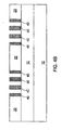
- a set of first primary lamellar structures 40 constitutes within each of the first openings O1 (See FIG. 1B ) constitutes a first one dimensional arrays of parallel lines having a sublithographic width and a sublithographic spacing. Variations of the present invention in which the first primary lamellar structures 40 are removed selective to the first complementary lamellar structures 50 and the first layer 20 by an anisotropic etch that removes the first polymeric block component selective to the second polymeric block component are explicitly contemplated herein.
- filler portions 22 are formed between the first primary lamellar structures 40.
- the filler portions 22 comprise a material that may be removed selective to the first primary lamellar structures 40 comprising the first polymeric block component.
- the filler portions may comprise a dielectric oxide, a dielectric nitride, or a porous or non-porous low dielectric constant material (having a dielectric constant less than the dielectric constant of silicon oxide, i.e., 3.9).
- the filler portions 22 may be formed by spin-on coating, deposition and recess etch, deposition and chemical mechanical planarization (CMP), or a combination thereof.
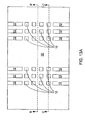
- a second layer 60 is formed as a blanket layer directly on the first layer 20, the first primary lamellar structures 40, and the filler portions 22.
- the second layer 60 may comprise any of the materials that may be employed as the first layer 20.
- the second layer 60 may comprise a semiconductor material, an insulator material, amorphous carbon, or diamond-like carbon.
- a spin-on coating or chemical vapor deposition may be employed to form the second layer 60.
- the thickness of the second layer 60 may be from about 3 nm to about 600 nm, and typically from about 10 nm to about 200 nm.
- the filler portion 22 and the second layer 60 may comprise the same material, and may be formed at the same processing step by forming the second layer 60 between the first primary lamellar structures 40. In this case, the filler portion 22 and the second layer 60 are integrally formed without any manifested physical interface therebetween.
- the second layer 60 is patterned by lithographic methods employing application of a photoresist (not shown), patterning of the photoresist, and an anisotropic etch that transfers the pattern in the photoresist into the second layer 60.
- the pattern contains a second opening 02 in the second layer 20.
- the second opening 02 may be formed through the second layer 60 to expose a top surface of the first layer 20, the first primary lamellar structures 40, and the filler portions 22, or alternately, may be formed only partly into the second layer 60 without exposing a top surface of the first layer 20.
- a second lateral width LW2, which is the lateral width of the second opening 02, is lithographic. More than one second opening 02 may be formed. In such a case, the spacing between adjacent second openings 02 is also lithographic.
- the second opening 02 has a shape of a rectangle or a parallelogram, and thus has two lengthwise edges that are longer than widthwise edges.
- the length of the second opening 02 which is the length of the lengthwise edges of the second openings 02, is an order of magnitude or more longer than the width of the second opening 02, which is the product of the length of the widthwise edges of the second opening 02 and the sine of the angle of one of the corners of the second opening 02. Since the second opening 02 is formed by lithographic methods, the length and the width of the second opening are lithographic dimensions.
- a second non-photosensitive polymeric resist is applied within the second opening 02 by methods well known in the art, such as spin coating to form second non-photosensitive polymeric resist portions 80.
- the top surface of the second non-photosensitive polymeric resist portions 80 may be recessed below, or substantially level with, the top surface of the second layer 60 outside the second opening 02.
- the second non-photosensitive polymeric resist may be applied to be coplanar with, or above, the top surfaces of the second layer 60, and then recessed to a final height by a recess etch, or by employing a dilute solution from which subsequent evaporation of a solvent causes volume contraction within the second opening 02.
- the second non-photosensitive polymeric resist comprises self-assembling block copolymers that are capable of self-organizing into nanometer-scale patterns.
- any of the material listed above for the first non-photosensitive polymeric resist may be employed for the second non-photosensitive polymeric resist.
- the second non-photosensitive polymeric resist may comprise the same material as, or a different material from the first photosensitive polymeric resist.
- the polymeric block components of the second non-photosensitive polymeric resist are referred to as a third polymeric block component and a fourth polymeric block component.
- the third polymeric block component may be the same as, or different from, the first polymeric block component.
- the fourth polymeric block component may be the same as, or different from, the second polymeric block component.
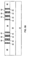
- a second nanoscale self-assembled self-aligned structure NS2 is formed within the second opening 02 by causing cross-linking of the self-assembling block copolymers through annealing.
- the same method employed for the formation of the first nanoscale self-assembled self-aligned structure NS1 may be employed to form the second nanoscale self-assembled self-aligned structures NS2.
- the second non-photosensitive polymeric resist is annealed by ultraviolet treatment or by thermal annealing at an elevated temperature to form second primary lamellar structures 90 comprising the third polymeric block component and second complementary lamellar structures 100 comprising the fourth polymeric block component.
- the second primary lamellar structure 90 and the second complementary lamellar structures 100 alternate with periodicity in the direction of the second lateral width LW2, i.e., in the direction perpendicular to the lengthwise edges of the second opening 02.
- composition and wetting properties of the second non-photosensitive polymeric resist is adjusted such that some of the second primary lamellar structures 90 abut the sidewalls of the second opening 02 in the second layer 60, while the second complementary lamellar structures 100 are disjoined from the sidewalls of the second opening 02 in the second layer 60.
- the wetting characteristics of the third polymeric block component is tuned so that the width of a second primary lamellar structure 90 abutting the sidewalls of the second opening 02 in the second layer 60 may be the same as, or different from, the width of another second primary lamellar structure 90 disjoined from the sidewalls of the second opening 02 in the second layer 60.
- the width of the second primary lamellar structures 90 may be sublithographic, and in the range from about 1 nm to about 40 nm, and typically from about 5 nm to about 30 nm.
- the width of the second complementary lamellar structures 100 which is herein referred to as a second lamellar spacing, may be sublithographic.
- the sum of the width of one of the second primary lamellar structures 90 and the second lamellar spacing may also be sublithographic.
- the second nanoscale self-assembled self-aligned structures NS2 are self-assembled and self-aligned in the same sense that the first nanoscale self-assembled self-aligned structures NS1 are self-assembled and self-aligned, since the same mechanism is employed for the self-assembly and self-alignment of the various components of the second nanoscale self-assembled self-aligned structures NS2.
- the second complementary lamellar structure 100 and the exposed portions of the second layer 60 are removed selective to the second primary lamellar structures 90 by an anisotropic etch such as a reactive ion etch. Top surfaces of the first layer 20, the filler portions 22, and the first primary lamellar structures 40 are exposed after the anisotropic etch.
- the second primary lamellar structures 90 are employed as an etch mask that contains a one dimensional array of lines having a sublithographic width and a sublithographic spacing.
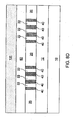
- the filler portions 22, the first layer 20 and the underlayer 12 are etched by an anisotropic etch such as a reactive ion etch selective to the second primary lamellar structures 90 and the first primary lamellar structures 40.
- the underlayer 12, as patterned with the patterns of the second primary lamellar structures 90 and the first primary lamellar structures 40, is herein referred to as a pattern-containing layer 12'.
- the second primary lamellar structures 90 and the first primary lamellar structures 40 as well as any remaining portions of the second layer 60, the filler portions 22, the first layer 20 that are located directly beneath the second primary lamellar structures 90 are removed selective to the pattern-containing layer 12' and the substrate 10.
- the pattern-containing layer 12' contains a plurality of nanoscale trenches having nanoscale dimensions, which is typically sublithographic.
- the pattern of the trench is formed by juxtaposition of two patterns having a periodicity in two different directions.
- the first pattern comprises the pattern of the first primary lamellar structures 40 containing a first set of sublithographic width lines separated by a sublithographic spacing, which is the first lamellar spacing, and repeated in the direction perpendicular to the lengthwise edges of the first openings O1 (See FIG. 1B ), which is herein referred to as a first direction.
- the second pattern comprises the pattern of the second primary lamellar structures 90 containing a second set of sublithographic width lines separated by another sublithographic spacing, which is the second lamellar spacing, and repeated in the direction perpendicular to the lengthwise edges of the second opening 02 (See FIG. 6C ), which is herein referred to as a second direction.
- the nanoscale trenches in the pattern-containing layer 12' is arranged in a two dimensional rectangular array or a two dimensional parallelogram-lattice array.
- the nanoscale trenches are repeated along the first direction and the second direction within the two dimensional array.
- Each of the nanoscale trenches has two pairs of sidewalls having a nanoscale dimension, i.e., a dimension from about 1 nm to about 40 nm, and typically from about 5 nm to about 30 nm.
- a second exemplary nanoscale structure according to a second embodiment of the present invention is derived from the first exemplary nanoscale structure of FIGS. 9A - 9C by removing the filler portions 22 and the underlayer 12 by an anisotropic etch such as a reactive ion etch selective to the first layer 20, the second primary lamellar structures 90, and the first primary lamellar structures 40.
- the underlayer 12, as patterned with the patterns of the second primary lamellar structures 90 and the first primary lamellar structures 40, is herein referred to as a pattern-containing layer 12'.
- the second embodiment only the portion of the pattern of the second primary lamellar structures 90 within the area of the first openings (See FIG. 1B ) are transferred into the pattern-containing layer 12' since the first layer 20 functions as an etch mask in combination with the second primary lamellar structures 90 and the first primary lamellar structures 40.
- the first layer 20, the first primary lamellar structures 40, and the second primary lamellar structures 90 as well as any remaining portions of the second layer 60, the filler portions 22, the first layer 20 that are located directly beneath the second primary lamellar structures 90 are removed selective to the pattern-containing layer 12' and the substrate 10.
- the pattern-containing layer 12' contains a plurality of nanoscale trenches having nanoscale dimensions, which is typically sublithographic.
- the pattern of the trench is formed by juxtaposition of two patterns having a periodicity in two different directions.
- the first pattern comprises the pattern of the first primary lamellar structures 40 containing a first set of sublithographic width lines separated by a sublithographic spacing, which is the first lamellar spacing, and repeated in the direction perpendicular to the lengthwise edges of the first openings O1 (See FIG. 1B ), which is herein referred to as a first direction.
- the second pattern comprises the pattern of the second primary lamellar structures 90 containing a second set of sublithographic width lines separated by another sublithographic spacing, which is the second lamellar spacing, and repeated in the direction perpendicular to the lengthwise edges of the second opening 02 (See FIG. 6C ), which is herein referred to as a second direction.
- the nanoscale trenches in the pattern-containing layer 12' is arranged in a two dimensional rectangular array or a two dimensional parallelogram-lattice array.
- the nanoscale trenches are repeated along the first direction and the second direction within the two dimensional array.
- Each of the nanoscale trenches has two pairs of sidewalls having a nanoscale dimension, i.e., a dimension from about 1 nm to about 40 nm, and typically from about 5 nm to about 30 nm.
- the nanoscale trenches may have a rectangular horizontal cross-sectional area.
- a generalized variation of the second exemplary nanoscale structure comprises a two dimensional parallelogram-lattice array of nanoscale trenches.
- Each of the nanoscale trenches has a set of first trench walls TW1 separated by a first width W1.
- a pair of first trench walls TW1 belonging to an adjacent pair of nanoscale trenches in the first direction, i.e., in the direction of the first nanoscale width W1, is separated by a first spacing S 1.
- Each of the first width W1 and the first spacing S1 is a nanoscale dimension, e.g., from about 1 nm to about 40 nm, and typically from about 5 nm to about 30 nm.
- each of the nanoscale trenches has a set of second trench walls TW2 separated by a second width W2.
- Each of the second width W2 and the second spacing S2 is a nanoscale dimension, e.g., from about 1 nm to about 40 nm, and typically from about 5 nm to about 30 nm.
- the angle ⁇ between the first direction and the second direction may be any arbitrary angle other than zero.
- the angle ⁇ may be between 0 degree and 60 degrees , 60 degrees , between 60 degrees and 90 degrees , or 90 degrees .
- the angle ⁇ between the first direction and the second direction is the same as an angle of a corner of a horizontal cross-sectional area of one of the nanoscale trenches, which is a parallelogram.
- the present invention enables an array of nanoscale trenches having sublithographic dimensions on the substrate 10.
- the present invention finds industrial applicability to the design and fabrication of two-dimensional self-assembled sublithographic nanoscale structures on a semiconductor substrate using a bottom-up fabrication process particularly suited to integrated circuit chips used in a large variety of electronic and electrical apparatus, and particularly useful to the computer and communication field.
Landscapes
- Engineering & Computer Science (AREA)
- Chemical & Material Sciences (AREA)
- Nanotechnology (AREA)
- Physics & Mathematics (AREA)
- Manufacturing & Machinery (AREA)
- Condensed Matter Physics & Semiconductors (AREA)
- General Physics & Mathematics (AREA)
- Microelectronics & Electronic Packaging (AREA)
- Crystallography & Structural Chemistry (AREA)
- Inorganic Chemistry (AREA)
- Computer Hardware Design (AREA)
- Power Engineering (AREA)
- Composite Materials (AREA)
- Materials Engineering (AREA)
- Mathematical Physics (AREA)
- Theoretical Computer Science (AREA)
- Analytical Chemistry (AREA)
- Exposure Of Semiconductors, Excluding Electron Or Ion Beam Exposure (AREA)
- Photosensitive Polymer And Photoresist Processing (AREA)
- Internal Circuitry In Semiconductor Integrated Circuit Devices (AREA)
- Formation Of Insulating Films (AREA)
Claims (14)
- Verfahren zum Bilden einer Struktur im Nanomaßstab auf einem Substrat (10), das Verfahren aufweisend:Bilden einer ersten ausgesparten Zone, welche eine untere Fläche aufweist, die sich durchgängig zwischen zwei parallelen ersten in Längsrichtung verlaufenden Rändern auf einer ersten Schicht (20) auf dem Substrat (10) erstreckt;Bilden einer ersten selbstassemblierten selbstausgerichteten Blockcopolymerstruktur im Nanomaßstab, welche mindestens eine erste Leitung enthält, die eine erste sublithographische Breite aufweist und erste Leitungsränder parallel zu den zwei parallelen ersten in Längsrichtung verlaufenden Rändern der ersten ausgesparten Zone aufweist;Bilden einer zweiten Schicht (60) als eine überdeckende Schicht, welche sich durchgängig über der ersten selbstassemblierten selbstausgerichteten Struktur im Nanomaßstab und über der ersten Schicht (20) erstreckt;Bilden einer zweiten ausgesparten Zone, welche zwei parallele zweite in Längsrichtung verlaufende Ränder auf der zweiten Schicht (60) aufweist, wobei ein Winkel zwischen den zwei parallelen ersten in Längsrichtung verlaufenden Rändern und den zwei parallelen zweiten in Längsrichtung verlaufenden Rändern größer als Null ist, wo sich die erste und zweite ausgesparte Zone kreuzen; undBilden einer zweiten selbstassemblierten selbstausgerichteten Blockcopolymerstruktur im Nanomaßstab, welche mindestens eine zweite Leitung enthält, die eine zweite sublithographische Breite aufweist und zweite Leitungsränder parallel zu den zwei parallelen zweiten in Längsrichtung verlaufenden Rändern der zweiten ausgesparten Zone aufweist.
- Verfahren nach Anspruch 1, wobei sich die erste selbstassemblierte selbstausgerichtete Struktur im Nanomaßstab an oder unterhalb einer oberen Fläche der ersten Schicht (20) befindet.
- Verfahren nach Anspruch 1, wobei sich die erste selbstassemblierte selbstausgerichtete Struktur im Nanomaßstab an oder unterhalb einer oberen Fläche der zweiten Schicht (60) befindet.
- Verfahren nach Anspruch 1, wobei der Schritt des Bildens des ersten selbstassemblierten selbstausgerichteten Blockcopolymerstruktur im Nanomaßstab Aufbringen eines ersten nicht lichtempfindlichen polymeren Resists, welcher eine erste polymere Komponente und eine zweite polymere Komponente aufweist, in der ersten ausgesparten Zone aufweist, wobei die mindestens eine erste Leitung die erste polymere Komponente aufweist.
- Verfahren nach Anspruch 4, ferner aufweisend:Bilden mindestens einer dritten Leitung, welche eine dritte sublithographische Breite aufweist, welche die zweite polymere Komponente aufweist und seitlich an die mindestens eine erste Leitung in der ersten ausgesparten Zone stößt; undEntfernen der mindestens einen dritten Leitung selektiv gegenüber der mindestens einen ersten Leitung und der ersten Schicht.
- Verfahren nach Anspruch 5, ferner aufweisend Füllen eines Raums, der durch das Entfernen der mindestens einen dritten Leitung gebildet wird, mit einem Füllmaterial, welches sich von dem ersten nicht lichtempfindlichen polymeren Resist unterscheidet.
- Verfahren nach Anspruch 1, wobei der Schritt des Bildens der zweiten selbstassemblierten selbstausgerichteten Blockcopolymerstruktur im Nanomaßstab Aufbringen eines zweiten nicht lichtempfindlichen polymeren Resists, welcher eine dritte polymere Komponente und eine vierte polymere Komponente aufweist, in der zweiten ausgesparten Zone aufweist, wobei die mindestens eine zweite Leitung die dritte polymere Komponente aufweist.
- Verfahren nach Anspruch 6, ferner aufweisend:Bilden mindestens einer vierten Leitung, welche eine vierte sublithographische Breite aufweist, welche die vierte polymere Komponente aufweist und seitlich an die mindestens eine zweite Leitung in der zweiten ausgesparten Zone stößt; undEntfernen der mindestens einen vierten Leitung selektiv gegenüber der mindestens einen zweiten Leitung und der zweiten Schicht.
- Verfahren nach Anspruch 1, wobei die mindestens eine erste Leitung eine polymere Komponente eines ersten nicht lichtempfindlichen polymeren Resists aufweist und die mindestens eine zweite Leitung eine polymere Komponente eines zweiten nicht lichtempfindlichen polymeren Resists aufweist, wobei das Verfahren ferner Entfernen der zweiten Schicht selektiv gegenüber der mindestens einen zweiten Leitung aufweist.
- Verfahren nach Anspruch 9, ferner aufweisend Entfernen der ersten Schicht selektiv gegenüber der mindestens einen ersten Leitung und der mindestens einen zweiten Leitung.
- Verfahren nach Anspruch 10, ferner aufweisend Bilden einer Struktur, welche ein zweidimensionales Feld von Gräben im Nanomaßstab in einer Unterschicht unterhalb der ersten Schicht und auf dem Substrat aufweist, wobei sich die Gräben im Nanomaßstab entlang einer ersten Richtung und einer zweiten Richtung innerhalb des zweidimensionalen Felds wiederholen und wobei jeder der Gräben im Nanomaßstab ein erstes Paar Seitenwände, die durch einen ersten sublithographischen Abstand getrennt sind, und ein zweites Paar Seitenwände aufweist, die durch einen zweiten sublithographischen Abstand getrennt sind.
- Verfahren nach Anspruch 11, wobei die erste Richtung senkrecht zu den zwei parallelen ersten in Längsrichtung verlaufenden Rändern verläuft und wobei die zweite Richtung senkrecht zu den zwei parallelen zweiten in Längsrichtung verlaufenden Rändern verläuft.
- Verfahren nach Anspruch 12, wobei eine horizontale Querschnittsfläche der Gräben im Nanomaßstab ein Parallelogramm ist.
- Verfahren nach Anspruch 13, wobei die horizontale Querschnittsfläche der Gräben im Nanomaßstab ein Rechteck ist.
Applications Claiming Priority (2)
| Application Number | Priority Date | Filing Date | Title |
|---|---|---|---|
| US12/017,598 US8207028B2 (en) | 2008-01-22 | 2008-01-22 | Two-dimensional patterning employing self-assembled material |
| PCT/US2009/031044 WO2009094282A1 (en) | 2008-01-22 | 2009-01-15 | Two-dimensional patterning employing self-assembled material |
Publications (3)
| Publication Number | Publication Date |
|---|---|
| EP2235743A1 EP2235743A1 (de) | 2010-10-06 |
| EP2235743A4 EP2235743A4 (de) | 2013-03-20 |
| EP2235743B1 true EP2235743B1 (de) | 2014-12-31 |
Family
ID=40901402
Family Applications (1)
| Application Number | Title | Priority Date | Filing Date |
|---|---|---|---|
| EP09704665.0A Not-in-force EP2235743B1 (de) | 2008-01-22 | 2009-01-15 | Zweidimensionale strukturierung unter verwendung eines selbstassemblierten materials |
Country Status (6)
| Country | Link |
|---|---|
| US (2) | US8207028B2 (de) |
| EP (1) | EP2235743B1 (de) |
| JP (1) | JP5505904B2 (de) |
| KR (1) | KR20100109937A (de) |
| TW (1) | TW200935499A (de) |
| WO (1) | WO2009094282A1 (de) |
Families Citing this family (15)
| Publication number | Priority date | Publication date | Assignee | Title |
|---|---|---|---|---|
| US8361704B2 (en) | 2009-01-12 | 2013-01-29 | International Business Machines Corporation | Method for reducing tip-to-tip spacing between lines |
| KR101096907B1 (ko) * | 2009-10-05 | 2011-12-22 | 주식회사 하이닉스반도체 | 반도체 소자 및 그 형성방법 |
| US8059350B2 (en) * | 2009-10-22 | 2011-11-15 | Hitachi Global Storage Technologies Netherlands B.V. | Patterned magnetic recording disk with patterned servo sectors having chevron servo patterns |
| FR2961344B1 (fr) * | 2010-06-09 | 2012-07-13 | Commissariat Energie Atomique | Procede de realisation d?une grille de lignes conductrices ou semi-conductrices d?acces croisees |
| US8673541B2 (en) * | 2010-10-29 | 2014-03-18 | Seagate Technology Llc | Block copolymer assembly methods and patterns formed thereby |
| FR2975823B1 (fr) * | 2011-05-27 | 2014-11-21 | Commissariat Energie Atomique | Procede de realisation d'un motif a la surface d'un bloc d'un substrat utilisant des copolymeres a bloc |
| JP5458136B2 (ja) * | 2012-03-28 | 2014-04-02 | 株式会社東芝 | パターン形成方法およびインプリントモールド製造方法 |
| JP5758363B2 (ja) * | 2012-09-07 | 2015-08-05 | 株式会社東芝 | パターン形成方法 |
| JP5537628B2 (ja) * | 2012-10-09 | 2014-07-02 | 株式会社東芝 | 自己組織化パターンの形成方法 |
| US9489974B2 (en) | 2014-04-11 | 2016-11-08 | Seagate Technology Llc | Method of fabricating a BPM template using hierarchical BCP density patterns |
| US9659824B2 (en) | 2015-04-28 | 2017-05-23 | International Business Machines Corporation | Graphoepitaxy directed self-assembly process for semiconductor fin formation |
| US9563122B2 (en) | 2015-04-28 | 2017-02-07 | International Business Machines Corporation | Method to harden photoresist for directed self-assembly processes |
| JP6809315B2 (ja) * | 2017-03-15 | 2021-01-06 | 東京エレクトロン株式会社 | 半導体装置の製造方法及び真空処理装置 |
| CN111081534B (zh) * | 2019-12-25 | 2023-10-27 | 上海集成电路研发中心有限公司 | 半导体纳米线的形成方法 |
| CN111128723B (zh) * | 2019-12-25 | 2023-09-15 | 上海集成电路研发中心有限公司 | 半导体纳米线的形成方法 |
Family Cites Families (21)
| Publication number | Priority date | Publication date | Assignee | Title |
|---|---|---|---|---|
| US4437226A (en) * | 1981-03-02 | 1984-03-20 | Rockwell International Corporation | Process for producing NPN type lateral transistor with minimal substrate operation interference |
| EP0059264A1 (de) * | 1981-03-02 | 1982-09-08 | Rockwell International Corporation | Lateraler NPN-Transistor mit minimaler Beeinflussung durch das Substrat und Verfahren zu seiner Herstellung |
| JPH0471293A (ja) | 1990-07-11 | 1992-03-05 | Cmk Corp | プリント配線板におけるスルーホール等への導電性物質等の充填方法 |
| US5587589A (en) | 1995-03-22 | 1996-12-24 | Motorola | Two dimensional organic light emitting diode array for high density information image manifestation apparatus |
| DE19526011C1 (de) * | 1995-07-17 | 1996-11-28 | Siemens Ag | Verfahren zur Herstellung von sublithographischen Ätzmasken |
| US6211039B1 (en) * | 1996-11-12 | 2001-04-03 | Micron Technology, Inc. | Silicon-on-insulator islands and method for their formation |
| US6777260B1 (en) | 2003-08-14 | 2004-08-17 | Silicon Storage Technology, Inc. | Method of making sub-lithographic sized contact holes |
| US6790745B1 (en) * | 2003-12-15 | 2004-09-14 | Jbcr Innovations | Fabrication of dielectrically isolated regions of silicon in a substrate |
| US8088293B2 (en) * | 2004-07-29 | 2012-01-03 | Micron Technology, Inc. | Methods of forming reticles configured for imprint lithography |
| US7247570B2 (en) * | 2004-08-19 | 2007-07-24 | Micron Technology, Inc. | Silicon pillars for vertical transistors |
| JP2006269763A (ja) * | 2005-03-24 | 2006-10-05 | Toshiba Corp | 集積回路装置の製造方法 |
| US7347953B2 (en) * | 2006-02-02 | 2008-03-25 | International Business Machines Corporation | Methods for forming improved self-assembled patterns of block copolymers |
| US7579278B2 (en) * | 2006-03-23 | 2009-08-25 | Micron Technology, Inc. | Topography directed patterning |
| US7407890B2 (en) | 2006-04-21 | 2008-08-05 | International Business Machines Corporation | Patterning sub-lithographic features with variable widths |
| JP4543004B2 (ja) * | 2006-05-11 | 2010-09-15 | 株式会社東芝 | パタン形成方法、インプリントモールド、および磁気記録媒体の製造方法 |
| US7723009B2 (en) * | 2006-06-02 | 2010-05-25 | Micron Technology, Inc. | Topography based patterning |
| US7605081B2 (en) | 2006-06-19 | 2009-10-20 | International Business Machines Corporation | Sub-lithographic feature patterning using self-aligned self-assembly polymers |
| JP4673266B2 (ja) * | 2006-08-03 | 2011-04-20 | 日本電信電話株式会社 | パターン形成方法及びモールド |
| JP4421582B2 (ja) * | 2006-08-15 | 2010-02-24 | 株式会社東芝 | パターン形成方法 |
| US8372295B2 (en) * | 2007-04-20 | 2013-02-12 | Micron Technology, Inc. | Extensions of self-assembled structures to increased dimensions via a “bootstrap” self-templating method |
| US8512849B2 (en) * | 2007-08-09 | 2013-08-20 | International Business Machines Corporation | Corrugated interfaces for multilayered interconnects |
-
2008
- 2008-01-22 US US12/017,598 patent/US8207028B2/en not_active Expired - Fee Related
-
2009
- 2009-01-05 TW TW098100104A patent/TW200935499A/zh unknown
- 2009-01-15 JP JP2010543218A patent/JP5505904B2/ja not_active Expired - Fee Related
- 2009-01-15 WO PCT/US2009/031044 patent/WO2009094282A1/en active Application Filing
- 2009-01-15 EP EP09704665.0A patent/EP2235743B1/de not_active Not-in-force
- 2009-01-15 KR KR1020107016678A patent/KR20100109937A/ko not_active Application Discontinuation
-
2012
- 2012-03-28 US US13/432,036 patent/US8754400B2/en not_active Expired - Fee Related
Also Published As
| Publication number | Publication date |
|---|---|
| WO2009094282A1 (en) | 2009-07-30 |
| US8754400B2 (en) | 2014-06-17 |
| US20120129357A1 (en) | 2012-05-24 |
| TW200935499A (en) | 2009-08-16 |
| US8207028B2 (en) | 2012-06-26 |
| JP5505904B2 (ja) | 2014-05-28 |
| JP2011523376A (ja) | 2011-08-11 |
| EP2235743A4 (de) | 2013-03-20 |
| EP2235743A1 (de) | 2010-10-06 |
| US20120183743A1 (en) | 2012-07-19 |
| KR20100109937A (ko) | 2010-10-11 |
Similar Documents
| Publication | Publication Date | Title |
|---|---|---|
| EP2235743B1 (de) | Zweidimensionale strukturierung unter verwendung eines selbstassemblierten materials | |
| EP2250123B1 (de) | Musterbildung mit selbstorganisiertem material | |
| US8921030B2 (en) | Tone inversion of self-assembled self-aligned structures | |
| US8361704B2 (en) | Method for reducing tip-to-tip spacing between lines | |
| US8716151B2 (en) | Method of fabricating semiconductor devices | |
| JP5559329B2 (ja) | 構造体および構造体を形成する方法 | |
| US9581899B2 (en) | 2-dimensional patterning employing tone inverted graphoepitaxy | |
| WO2008094746A2 (en) | Sub-lithographic interconnect patterning using self-assembling polymers | |
| US9691615B2 (en) | Chemoepitaxy-based directed self assembly process with tone inversion for unidirectional wiring | |
| CN111261586B (zh) | 一种中孔半导体纳米结构的制作方法 | |
| US20090117360A1 (en) | Self-assembled material pattern transfer contrast enhancement | |
| US20140353762A1 (en) | Multi-orientation semiconductor devices employing directed self-assembly |
Legal Events
| Date | Code | Title | Description |
|---|---|---|---|
| PUAI | Public reference made under article 153(3) epc to a published international application that has entered the european phase |
Free format text: ORIGINAL CODE: 0009012 |
|
| 17P | Request for examination filed |
Effective date: 20100728 |
|
| AK | Designated contracting states |
Kind code of ref document: A1 Designated state(s): AT BE BG CH CY CZ DE DK EE ES FI FR GB GR HR HU IE IS IT LI LT LU LV MC MK MT NL NO PL PT RO SE SI SK TR |
|
| AX | Request for extension of the european patent |
Extension state: AL BA RS |
|
| RIN1 | Information on inventor provided before grant (corrected) |
Inventor name: RADENS, CARL Inventor name: KIM, HO-CHEOL Inventor name: DORIS, BRUCE, B. Inventor name: DALTON, TIMOTHY |
|
| DAX | Request for extension of the european patent (deleted) | ||
| REG | Reference to a national code |
Ref country code: DE Ref legal event code: R079 Ref document number: 602009028663 Country of ref document: DE Free format text: PREVIOUS MAIN CLASS: H01L0021321300 Ipc: H01L0021033000 |
|
| A4 | Supplementary search report drawn up and despatched |
Effective date: 20130219 |
|
| RIC1 | Information provided on ipc code assigned before grant |
Ipc: B81C 1/00 20060101ALI20130213BHEP Ipc: H01L 21/033 20060101AFI20130213BHEP |
|
| GRAP | Despatch of communication of intention to grant a patent |
Free format text: ORIGINAL CODE: EPIDOSNIGR1 |
|
| INTG | Intention to grant announced |
Effective date: 20140108 |
|
| GRAP | Despatch of communication of intention to grant a patent |
Free format text: ORIGINAL CODE: EPIDOSNIGR1 |
|
| GRAS | Grant fee paid |
Free format text: ORIGINAL CODE: EPIDOSNIGR3 |
|
| INTG | Intention to grant announced |
Effective date: 20141031 |
|
| GRAA | (expected) grant |
Free format text: ORIGINAL CODE: 0009210 |
|
| AK | Designated contracting states |
Kind code of ref document: B1 Designated state(s): AT BE BG CH CY CZ DE DK EE ES FI FR GB GR HR HU IE IS IT LI LT LU LV MC MK MT NL NO PL PT RO SE SI SK TR |
|
| REG | Reference to a national code |
Ref country code: CH Ref legal event code: EP Ref country code: GB Ref legal event code: FG4D |
|
| REG | Reference to a national code |
Ref country code: CH Ref legal event code: NV Representative=s name: IBM RESEARCH GMBH ZURICH RESEARCH LABORATORY I, CH Ref country code: DE Ref legal event code: R084 Ref document number: 602009028663 Country of ref document: DE |
|
| REG | Reference to a national code |
Ref country code: IE Ref legal event code: FG4D |
|
| REG | Reference to a national code |
Ref country code: AT Ref legal event code: REF Ref document number: 704840 Country of ref document: AT Kind code of ref document: T Effective date: 20150215 |
|
| REG | Reference to a national code |
Ref country code: DE Ref legal event code: R096 Ref document number: 602009028663 Country of ref document: DE Effective date: 20150219 |
|
| REG | Reference to a national code |
Ref country code: GB Ref legal event code: 746 Effective date: 20150203 |
|
| REG | Reference to a national code |
Ref country code: DE Ref legal event code: R084 Ref document number: 602009028663 Country of ref document: DE Effective date: 20150115 |
|
| PG25 | Lapsed in a contracting state [announced via postgrant information from national office to epo] |
Ref country code: FI Free format text: LAPSE BECAUSE OF FAILURE TO SUBMIT A TRANSLATION OF THE DESCRIPTION OR TO PAY THE FEE WITHIN THE PRESCRIBED TIME-LIMIT Effective date: 20141231 Ref country code: LT Free format text: LAPSE BECAUSE OF FAILURE TO SUBMIT A TRANSLATION OF THE DESCRIPTION OR TO PAY THE FEE WITHIN THE PRESCRIBED TIME-LIMIT Effective date: 20141231 Ref country code: NO Free format text: LAPSE BECAUSE OF FAILURE TO SUBMIT A TRANSLATION OF THE DESCRIPTION OR TO PAY THE FEE WITHIN THE PRESCRIBED TIME-LIMIT Effective date: 20150331 |
|
| REG | Reference to a national code |
Ref country code: NL Ref legal event code: VDEP Effective date: 20141231 |
|
| REG | Reference to a national code |
Ref country code: LT Ref legal event code: MG4D |
|
| PG25 | Lapsed in a contracting state [announced via postgrant information from national office to epo] |
Ref country code: GR Free format text: LAPSE BECAUSE OF FAILURE TO SUBMIT A TRANSLATION OF THE DESCRIPTION OR TO PAY THE FEE WITHIN THE PRESCRIBED TIME-LIMIT Effective date: 20150401 Ref country code: LV Free format text: LAPSE BECAUSE OF FAILURE TO SUBMIT A TRANSLATION OF THE DESCRIPTION OR TO PAY THE FEE WITHIN THE PRESCRIBED TIME-LIMIT Effective date: 20141231 Ref country code: SE Free format text: LAPSE BECAUSE OF FAILURE TO SUBMIT A TRANSLATION OF THE DESCRIPTION OR TO PAY THE FEE WITHIN THE PRESCRIBED TIME-LIMIT Effective date: 20141231 Ref country code: HR Free format text: LAPSE BECAUSE OF FAILURE TO SUBMIT A TRANSLATION OF THE DESCRIPTION OR TO PAY THE FEE WITHIN THE PRESCRIBED TIME-LIMIT Effective date: 20141231 |
|
| PGFP | Annual fee paid to national office [announced via postgrant information from national office to epo] |
Ref country code: GB Payment date: 20150218 Year of fee payment: 7 |
|
| REG | Reference to a national code |
Ref country code: AT Ref legal event code: MK05 Ref document number: 704840 Country of ref document: AT Kind code of ref document: T Effective date: 20141231 |
|
| PG25 | Lapsed in a contracting state [announced via postgrant information from national office to epo] |
Ref country code: NL Free format text: LAPSE BECAUSE OF FAILURE TO SUBMIT A TRANSLATION OF THE DESCRIPTION OR TO PAY THE FEE WITHIN THE PRESCRIBED TIME-LIMIT Effective date: 20141231 |
|
| PG25 | Lapsed in a contracting state [announced via postgrant information from national office to epo] |
Ref country code: RO Free format text: LAPSE BECAUSE OF FAILURE TO SUBMIT A TRANSLATION OF THE DESCRIPTION OR TO PAY THE FEE WITHIN THE PRESCRIBED TIME-LIMIT Effective date: 20141231 Ref country code: SK Free format text: LAPSE BECAUSE OF FAILURE TO SUBMIT A TRANSLATION OF THE DESCRIPTION OR TO PAY THE FEE WITHIN THE PRESCRIBED TIME-LIMIT Effective date: 20141231 Ref country code: CZ Free format text: LAPSE BECAUSE OF FAILURE TO SUBMIT A TRANSLATION OF THE DESCRIPTION OR TO PAY THE FEE WITHIN THE PRESCRIBED TIME-LIMIT Effective date: 20141231 Ref country code: ES Free format text: LAPSE BECAUSE OF FAILURE TO SUBMIT A TRANSLATION OF THE DESCRIPTION OR TO PAY THE FEE WITHIN THE PRESCRIBED TIME-LIMIT Effective date: 20141231 |
|
| REG | Reference to a national code |
Ref country code: CH Ref legal event code: PL |
|
| PG25 | Lapsed in a contracting state [announced via postgrant information from national office to epo] |
Ref country code: PL Free format text: LAPSE BECAUSE OF FAILURE TO SUBMIT A TRANSLATION OF THE DESCRIPTION OR TO PAY THE FEE WITHIN THE PRESCRIBED TIME-LIMIT Effective date: 20141231 Ref country code: AT Free format text: LAPSE BECAUSE OF FAILURE TO SUBMIT A TRANSLATION OF THE DESCRIPTION OR TO PAY THE FEE WITHIN THE PRESCRIBED TIME-LIMIT Effective date: 20141231 Ref country code: LU Free format text: LAPSE BECAUSE OF FAILURE TO SUBMIT A TRANSLATION OF THE DESCRIPTION OR TO PAY THE FEE WITHIN THE PRESCRIBED TIME-LIMIT Effective date: 20150115 Ref country code: IS Free format text: LAPSE BECAUSE OF FAILURE TO SUBMIT A TRANSLATION OF THE DESCRIPTION OR TO PAY THE FEE WITHIN THE PRESCRIBED TIME-LIMIT Effective date: 20150430 |
|
| REG | Reference to a national code |
Ref country code: DE Ref legal event code: R097 Ref document number: 602009028663 Country of ref document: DE |
|
| PG25 | Lapsed in a contracting state [announced via postgrant information from national office to epo] |
Ref country code: EE Free format text: LAPSE BECAUSE OF FAILURE TO SUBMIT A TRANSLATION OF THE DESCRIPTION OR TO PAY THE FEE WITHIN THE PRESCRIBED TIME-LIMIT Effective date: 20141231 Ref country code: LI Free format text: LAPSE BECAUSE OF NON-PAYMENT OF DUE FEES Effective date: 20150131 Ref country code: CH Free format text: LAPSE BECAUSE OF NON-PAYMENT OF DUE FEES Effective date: 20150131 Ref country code: DK Free format text: LAPSE BECAUSE OF FAILURE TO SUBMIT A TRANSLATION OF THE DESCRIPTION OR TO PAY THE FEE WITHIN THE PRESCRIBED TIME-LIMIT Effective date: 20141231 Ref country code: MC Free format text: LAPSE BECAUSE OF FAILURE TO SUBMIT A TRANSLATION OF THE DESCRIPTION OR TO PAY THE FEE WITHIN THE PRESCRIBED TIME-LIMIT Effective date: 20141231 |
|
| REG | Reference to a national code |
Ref country code: IE Ref legal event code: MM4A |
|
| PLBE | No opposition filed within time limit |
Free format text: ORIGINAL CODE: 0009261 |
|
| STAA | Information on the status of an ep patent application or granted ep patent |
Free format text: STATUS: NO OPPOSITION FILED WITHIN TIME LIMIT |
|
| 26N | No opposition filed |
Effective date: 20151001 |
|
| REG | Reference to a national code |
Ref country code: FR Ref legal event code: ST Effective date: 20151117 |
|
| PG25 | Lapsed in a contracting state [announced via postgrant information from national office to epo] |
Ref country code: IT Free format text: LAPSE BECAUSE OF FAILURE TO SUBMIT A TRANSLATION OF THE DESCRIPTION OR TO PAY THE FEE WITHIN THE PRESCRIBED TIME-LIMIT Effective date: 20141231 |
|
| PG25 | Lapsed in a contracting state [announced via postgrant information from national office to epo] |
Ref country code: IE Free format text: LAPSE BECAUSE OF NON-PAYMENT OF DUE FEES Effective date: 20150115 |
|
| PG25 | Lapsed in a contracting state [announced via postgrant information from national office to epo] |
Ref country code: FR Free format text: LAPSE BECAUSE OF NON-PAYMENT OF DUE FEES Effective date: 20150302 Ref country code: SI Free format text: LAPSE BECAUSE OF FAILURE TO SUBMIT A TRANSLATION OF THE DESCRIPTION OR TO PAY THE FEE WITHIN THE PRESCRIBED TIME-LIMIT Effective date: 20141231 |
|
| REG | Reference to a national code |
Ref country code: DE Ref legal event code: R081 Ref document number: 602009028663 Country of ref document: DE Owner name: GLOBALFOUNDRIES INC., KY Free format text: FORMER OWNER: INTERNATIONAL BUSINESS MACHINES CORPORATION, ARMONK, NY, US Ref country code: DE Ref legal event code: R082 Ref document number: 602009028663 Country of ref document: DE Representative=s name: RICHARDT PATENTANWAELTE PARTG MBB, DE Ref country code: DE Ref legal event code: R081 Ref document number: 602009028663 Country of ref document: DE Owner name: GLOBALFOUNDRIES INC., KY Free format text: FORMER OWNER: INTERNATIONAL BUSINESS MACHINES CORPORATION, ARMONK, N.Y., US |
|
| REG | Reference to a national code |
Ref country code: DE Ref legal event code: R081 Ref document number: 602009028663 Country of ref document: DE Owner name: GLOBALFOUNDRIES INC., KY Free format text: FORMER OWNER: GLOBALFOUNDRIES US 2 LLC (N.D.GES.DES STAATES DELAWARE), HOPEWELL JUNCTION, N.Y., US Ref country code: DE Ref legal event code: R082 Ref document number: 602009028663 Country of ref document: DE Representative=s name: RICHARDT PATENTANWAELTE PARTG MBB, DE |
|
| PG25 | Lapsed in a contracting state [announced via postgrant information from national office to epo] |
Ref country code: BE Free format text: LAPSE BECAUSE OF FAILURE TO SUBMIT A TRANSLATION OF THE DESCRIPTION OR TO PAY THE FEE WITHIN THE PRESCRIBED TIME-LIMIT Effective date: 20141231 |
|
| GBPC | Gb: european patent ceased through non-payment of renewal fee |
Effective date: 20160115 |
|
| PG25 | Lapsed in a contracting state [announced via postgrant information from national office to epo] |
Ref country code: GB Free format text: LAPSE BECAUSE OF NON-PAYMENT OF DUE FEES Effective date: 20160115 |
|
| PG25 | Lapsed in a contracting state [announced via postgrant information from national office to epo] |
Ref country code: MT Free format text: LAPSE BECAUSE OF FAILURE TO SUBMIT A TRANSLATION OF THE DESCRIPTION OR TO PAY THE FEE WITHIN THE PRESCRIBED TIME-LIMIT Effective date: 20141231 |
|
| PG25 | Lapsed in a contracting state [announced via postgrant information from national office to epo] |
Ref country code: BG Free format text: LAPSE BECAUSE OF FAILURE TO SUBMIT A TRANSLATION OF THE DESCRIPTION OR TO PAY THE FEE WITHIN THE PRESCRIBED TIME-LIMIT Effective date: 20141231 Ref country code: HU Free format text: LAPSE BECAUSE OF FAILURE TO SUBMIT A TRANSLATION OF THE DESCRIPTION OR TO PAY THE FEE WITHIN THE PRESCRIBED TIME-LIMIT; INVALID AB INITIO Effective date: 20090115 |
|
| PG25 | Lapsed in a contracting state [announced via postgrant information from national office to epo] |
Ref country code: CY Free format text: LAPSE BECAUSE OF FAILURE TO SUBMIT A TRANSLATION OF THE DESCRIPTION OR TO PAY THE FEE WITHIN THE PRESCRIBED TIME-LIMIT Effective date: 20141231 |
|
| PG25 | Lapsed in a contracting state [announced via postgrant information from national office to epo] |
Ref country code: PT Free format text: LAPSE BECAUSE OF FAILURE TO SUBMIT A TRANSLATION OF THE DESCRIPTION OR TO PAY THE FEE WITHIN THE PRESCRIBED TIME-LIMIT Effective date: 20150501 |
|
| PG25 | Lapsed in a contracting state [announced via postgrant information from national office to epo] |
Ref country code: TR Free format text: LAPSE BECAUSE OF FAILURE TO SUBMIT A TRANSLATION OF THE DESCRIPTION OR TO PAY THE FEE WITHIN THE PRESCRIBED TIME-LIMIT Effective date: 20141231 |
|
| PGFP | Annual fee paid to national office [announced via postgrant information from national office to epo] |
Ref country code: DE Payment date: 20180103 Year of fee payment: 10 |
|
| PG25 | Lapsed in a contracting state [announced via postgrant information from national office to epo] |
Ref country code: MK Free format text: LAPSE BECAUSE OF FAILURE TO SUBMIT A TRANSLATION OF THE DESCRIPTION OR TO PAY THE FEE WITHIN THE PRESCRIBED TIME-LIMIT Effective date: 20141231 |
|
| REG | Reference to a national code |
Ref country code: DE Ref legal event code: R119 Ref document number: 602009028663 Country of ref document: DE |
|
| PG25 | Lapsed in a contracting state [announced via postgrant information from national office to epo] |
Ref country code: DE Free format text: LAPSE BECAUSE OF NON-PAYMENT OF DUE FEES Effective date: 20190801 |