EP2183794B1 - Led-gehäuse - Google Patents
Led-gehäuse Download PDFInfo
- Publication number
- EP2183794B1 EP2183794B1 EP08801127.5A EP08801127A EP2183794B1 EP 2183794 B1 EP2183794 B1 EP 2183794B1 EP 08801127 A EP08801127 A EP 08801127A EP 2183794 B1 EP2183794 B1 EP 2183794B1
- Authority
- EP
- European Patent Office
- Prior art keywords
- led
- housing
- led housing
- connection
- carrier
- Prior art date
- Legal status (The legal status is an assumption and is not a legal conclusion. Google has not performed a legal analysis and makes no representation as to the accuracy of the status listed.)
- Not-in-force
Links
Images


Classifications
-
- H—ELECTRICITY
- H10—SEMICONDUCTOR DEVICES; ELECTRIC SOLID-STATE DEVICES NOT OTHERWISE PROVIDED FOR
- H10H—INORGANIC LIGHT-EMITTING SEMICONDUCTOR DEVICES HAVING POTENTIAL BARRIERS
- H10H20/00—Individual inorganic light-emitting semiconductor devices having potential barriers, e.g. light-emitting diodes [LED]
- H10H20/80—Constructional details
- H10H20/85—Packages
-
- F—MECHANICAL ENGINEERING; LIGHTING; HEATING; WEAPONS; BLASTING
- F21—LIGHTING
- F21S—NON-PORTABLE LIGHTING DEVICES; SYSTEMS THEREOF; VEHICLE LIGHTING DEVICES SPECIALLY ADAPTED FOR VEHICLE EXTERIORS
- F21S2/00—Systems of lighting devices, not provided for in main groups F21S4/00 - F21S10/00 or F21S19/00, e.g. of modular construction
- F21S2/005—Systems of lighting devices, not provided for in main groups F21S4/00 - F21S10/00 or F21S19/00, e.g. of modular construction of modular construction
-
- F—MECHANICAL ENGINEERING; LIGHTING; HEATING; WEAPONS; BLASTING
- F21—LIGHTING
- F21K—NON-ELECTRIC LIGHT SOURCES USING LUMINESCENCE; LIGHT SOURCES USING ELECTROCHEMILUMINESCENCE; LIGHT SOURCES USING CHARGES OF COMBUSTIBLE MATERIAL; LIGHT SOURCES USING SEMICONDUCTOR DEVICES AS LIGHT-GENERATING ELEMENTS; LIGHT SOURCES NOT OTHERWISE PROVIDED FOR
- F21K9/00—Light sources using semiconductor devices as light-generating elements, e.g. using light-emitting diodes [LED] or lasers
-
- H—ELECTRICITY
- H01—ELECTRIC ELEMENTS
- H01L—SEMICONDUCTOR DEVICES NOT COVERED BY CLASS H10
- H01L25/00—Assemblies consisting of a plurality of semiconductor or other solid state devices
- H01L25/03—Assemblies consisting of a plurality of semiconductor or other solid state devices all the devices being of a type provided for in a single subclass of subclasses H10B, H10D, H10F, H10H, H10K or H10N, e.g. assemblies of rectifier diodes
- H01L25/04—Assemblies consisting of a plurality of semiconductor or other solid state devices all the devices being of a type provided for in a single subclass of subclasses H10B, H10D, H10F, H10H, H10K or H10N, e.g. assemblies of rectifier diodes the devices not having separate containers
- H01L25/075—Assemblies consisting of a plurality of semiconductor or other solid state devices all the devices being of a type provided for in a single subclass of subclasses H10B, H10D, H10F, H10H, H10K or H10N, e.g. assemblies of rectifier diodes the devices not having separate containers the devices being of a type provided for in group H10H20/00
- H01L25/0753—Assemblies consisting of a plurality of semiconductor or other solid state devices all the devices being of a type provided for in a single subclass of subclasses H10B, H10D, H10F, H10H, H10K or H10N, e.g. assemblies of rectifier diodes the devices not having separate containers the devices being of a type provided for in group H10H20/00 the devices being arranged next to each other
-
- H—ELECTRICITY
- H01—ELECTRIC ELEMENTS
- H01R—ELECTRICALLY-CONDUCTIVE CONNECTIONS; STRUCTURAL ASSOCIATIONS OF A PLURALITY OF MUTUALLY-INSULATED ELECTRICAL CONNECTING ELEMENTS; COUPLING DEVICES; CURRENT COLLECTORS
- H01R13/00—Details of coupling devices of the kinds covered by groups H01R12/70 or H01R24/00 - H01R33/00
- H01R13/02—Contact members
- H01R13/10—Sockets for co-operation with pins or blades
- H01R13/11—Resilient sockets
- H01R13/113—Resilient sockets co-operating with pins or blades having a rectangular transverse section
-
- H—ELECTRICITY
- H10—SEMICONDUCTOR DEVICES; ELECTRIC SOLID-STATE DEVICES NOT OTHERWISE PROVIDED FOR
- H10H—INORGANIC LIGHT-EMITTING SEMICONDUCTOR DEVICES HAVING POTENTIAL BARRIERS
- H10H20/00—Individual inorganic light-emitting semiconductor devices having potential barriers, e.g. light-emitting diodes [LED]
- H10H20/80—Constructional details
- H10H20/85—Packages
- H10H20/8506—Containers
-
- F—MECHANICAL ENGINEERING; LIGHTING; HEATING; WEAPONS; BLASTING
- F21—LIGHTING
- F21Y—INDEXING SCHEME ASSOCIATED WITH SUBCLASSES F21K, F21L, F21S and F21V, RELATING TO THE FORM OR THE KIND OF THE LIGHT SOURCES OR OF THE COLOUR OF THE LIGHT EMITTED
- F21Y2115/00—Light-generating elements of semiconductor light sources
- F21Y2115/10—Light-emitting diodes [LED]
-
- H—ELECTRICITY
- H01—ELECTRIC ELEMENTS
- H01L—SEMICONDUCTOR DEVICES NOT COVERED BY CLASS H10
- H01L2224/00—Indexing scheme for arrangements for connecting or disconnecting semiconductor or solid-state bodies and methods related thereto as covered by H01L24/00
- H01L2224/01—Means for bonding being attached to, or being formed on, the surface to be connected, e.g. chip-to-package, die-attach, "first-level" interconnects; Manufacturing methods related thereto
- H01L2224/42—Wire connectors; Manufacturing methods related thereto
- H01L2224/47—Structure, shape, material or disposition of the wire connectors after the connecting process
- H01L2224/48—Structure, shape, material or disposition of the wire connectors after the connecting process of an individual wire connector
- H01L2224/4805—Shape
- H01L2224/4809—Loop shape
- H01L2224/48091—Arched
-
- H—ELECTRICITY
- H01—ELECTRIC ELEMENTS
- H01L—SEMICONDUCTOR DEVICES NOT COVERED BY CLASS H10
- H01L2224/00—Indexing scheme for arrangements for connecting or disconnecting semiconductor or solid-state bodies and methods related thereto as covered by H01L24/00
- H01L2224/01—Means for bonding being attached to, or being formed on, the surface to be connected, e.g. chip-to-package, die-attach, "first-level" interconnects; Manufacturing methods related thereto
- H01L2224/42—Wire connectors; Manufacturing methods related thereto
- H01L2224/47—Structure, shape, material or disposition of the wire connectors after the connecting process
- H01L2224/48—Structure, shape, material or disposition of the wire connectors after the connecting process of an individual wire connector
- H01L2224/481—Disposition
- H01L2224/48135—Connecting between different semiconductor or solid-state bodies, i.e. chip-to-chip
- H01L2224/48137—Connecting between different semiconductor or solid-state bodies, i.e. chip-to-chip the bodies being arranged next to each other, e.g. on a common substrate
Definitions
- the invention relates to an LED housing having a housing cavity, a carrier element, an LED chip, a holding element and at least one housing connection element, wherein the housing is designed such that it can be extended modularly by a second identical LED housing. Furthermore, the housing can be mounted in various ways on a support and has an optimal heat dissipation.
- the publication US2006 / 0262533 A1 describes a modular light-emitting diode.
- the publication DE 102 42 292 A1 describes a surface lamp.
- Light-emitting diodes also known as light-emitting diodes or light-emitting diodes (LEDs) are optoelectronic components which, in their operation, emit electromagnetic radiation with wavelengths in the ultraviolet, infrared but also in the part of the electromagnetic spectrum which is perceptible to the human eye.
- LEDs are used as status indicators, bulbs of different wavelengths, indicator lights, for Data transmission, used in display elements and much more.
- light-emitting diodes in special semiconductor grid structures use, in particular, the energy gap between conduction band and valence band.
- the difference between the energy levels of the valence band and the conduction band is understood as bandgap or band gap, with the direct band transition semiconductor materials being the highest energetic state in the valence band directly below the lowest energetic state of the conduction band.
- the direct band transition semiconductor materials being the highest energetic state in the valence band directly below the lowest energetic state of the conduction band.
- a luminescence conversion element By introducing a luminescence conversion element into the beam path of the emitting semiconductor, it is possible to convert the primary generated wavelength into a secondary wavelength. Thus, it is possible to easily generate mixed light, for example white light or light of a specific wavelength, which does not correspond to the band gap of the respective semiconductor.
- a light-emitting diode can now be mounted in different ways.
- LEDs can be mounted on a printed circuit board using Surface-Mount Technology (SMT).
- SMT Surface-Mount Technology
- connection legs for mounting on a perforated printed circuit board.
- the provided for electrical operation connections must be specially designed.
- a light-emitting diode chip in a housing preferably a partially transparent for the emitting wavelength potting material introduced.
- the electrical connection of the emitting chip now takes place via discrete, led out of the housing additional connection legs.
- LED Additional elements such as socket adapter pieces that electrically and / or mechanically connect a conventional LED by means of plug-in systems and / or brackets.
- backlights for liquid crystal displays including liquid crystal displays (LCD) are generated by means of white light LED matrix, with a matrix of a plurality of white light LEDs serving as a backlight.
- the invention is therefore based on the object to provide an LED housing which can be mounted in various ways and beyond modular with another identical LED housing can be expanded.
- an LED housing which has a housing cavity, a carrier element, at least one LED chip, at least one holding element and at least one housing connection element is shown.
- the carrier element is equipped on a first upper side with at least one LED chip and disposed within the housing cavity in the LED housing.
- the LED housing is formed such that the at least one housing connection element is arranged on an outer side of the LED housing and has an electrical connection to the at least one LED chip for operating this LED chip and furthermore the LED housing mechanically detachable can be connected to a second identical LED housing.
- “Mechanically solvable” may mean that the connection is due to mechanical force solvable. Wherein the connection is preferably non-destructively detachable, so that after loosening two identical LED housing from each other at least one of the LED housing can be reused.
- the described subject matter provides an LED housing which can be flexibly used for a wide variety of installation variants, can be electrically connected flexibly and, moreover, can be mechanically connected or expanded without additional elements having a further identical LED housing.
- the LED housing is mechanically detachable mechanically connected by means of at least one holding element with a carrier.
- a carrier in the context of the invention is for example a heat sink, a circuit board or generally a heat sink.
- a carrier in general a base body can be described, which offers the LED housing enough holding power in its specific application.
- a heat sink so he ensures good heat conduction properties for a sufficiently high heat dissipation and thereby prevents destruction of the LED chip within the housing cavity.
- a sufficient holding force for the mechanical connection with the carrier is achieved by at least one holding element.
- the retaining element is either a part of the LED housing or attached as an additional element to the LED housing.
- a holding element here is a hole made in the LED housing, through which a mechanical connecting element, for example a screw or a retaining pin, is guided.
- the holding element is either attached as a separate element on the LED housing or formed as part of the housing.
- the LED housing has a mechanical and / or electrical connection to a structurally identical LED housing by at least one holding element.
- the LED housing additionally has a heat dissipation element which is located at least on a second side of the carrier element. This second side is opposite the first top side of the carrier element.
- the holding element is in several parts and the housing connecting element is integrated in at least one part of the holding element.
- This is a universal modular expansion to a similar LED housing or a carrier possible, wherein at least a part of the holding element also provides the electrical connection between the LED chips.
- the mechanical connection force to a carrier or a second LED housing is generated by the holding element.
- the retaining element is then in one piece and thus generates, for example by a plug-in system, the electrical and mechanical connection. By this measure, a rapid expansion of an LED housing is achieved.
- the housing connection element has at least one anode connection element and one cathode connection element.
- These two connection elements can be advantageously designed as a mechanical and / or electrical plug-in system, wherein the anode connection element, for example, a socket and the cathode connection element, for example, a plug or vice versa.
- the anode connection element for example, a socket
- the cathode connection element for example, a plug or vice versa.
- the housing cavity of the LED housing has a plurality of LED chips. These LED chips are in the first embodiment in FIG Series connected, wherein each anode terminal of an LED chip is connected to a cathode terminal of an adjacent LED chip. A first anode terminal serving as a common anode terminal of the LED package and a last cathode terminal serving as a common cathode terminal of the LED package are led to the package terminal of the LED package.
- all LED chips within this LED housing via a common, in a special form multi-part, housing connection element are electrically controlled.
- the radiated light intensity of a single LED housing already increases enormous.
- it is possible to produce mixed colors within an LED housing wherein each LED chip emits a specific wavelength, in the example of a mixing lamp, for example, a white light would be generated, which is very easy by the color combination red, green and blue.
- the housing connection element via connectors or latching connector is electrically driven
- the LED housing is basically SMT-mounted.
- a good heat dissipation to the SMT board is created on the turn, in addition, a heat sink, for example in the form of a heat sink can be present.
- a heat sink for example in the form of a heat sink can be present.
- the housing connection element is also SMT-mounted, whereby the electrical connection also takes place via the SMT board. The same applies, of course, for other forms of installation.
- a control connection element is additionally attached to the LED housing.
- This control connection element has an electrical connection to at least one control element within the housing cavity.
- This control in turn controls the intensity of the emitted electromagnetic radiation of one of the LED chips within the housing cavity.
- PWM pulse width modulated
- each LED chip is led individually to the housing connection element.
- each LED chip can be controlled separately and thus switched on and off.
- the carrier element is a direct-bonded copper ceramic substrate (DBC ceramic).
- DBC ceramic direct-bonded copper ceramic substrate
- This type of substrate which is a "sandwich construction" of copper-ceramic-copper, provides electrical insulation. Furthermore, a laterally spread heat dissipation is generated by this kind of substrate, whereby a good heat dissipation occurs.
- this substrate is electrically very conductive.
- the carrier substrate is a metallic carrier, for example copper or copper alloy with bonding metallization.
- the LED chip backs must be made electrically insulating.
- connection of the LED chips to the housing connection element is preferably carried out by laser welding and / or bonding method. In this way, a faster production can be achieved.
- the LED housing additionally has an optical element or holders for such an optical element, for example a lens or a lens-like capping.
- an optical element for example a lens or a lens-like capping.
- this optical element is a beam bundling, beam expansion or generally a beam deflection can be achieved. This achieves a targeted emission characteristic of the LED.
- the LED housing is made of a Vergussmassematerial. This potting compound material is fluid during the manufacturing process and is formed into the desired LED package shape by fitting.
- At least a part of the holding element is formed separately or standardized with the housing connection elements. Due to the standardized shape, as found in many areas, such as in the automotive sector, a maximum range of use of this LED housing is possible.
- the inventive electrical and / or mechanical in series connecting a plurality of LED housing is done for example by plugging, notching, or screws. Furthermore is also a parallel connection of this LED housing conceivable, which can be achieved by an additional adapter piece.
- This adapter piece is for example mounted between two anode connection elements and serves for electrical bridging. Furthermore, the adapter piece serves as a spacer between the parallel connected LED housings.
- an additional bridge adapter is also included within the scope of the invention. This bridge adapter is used for the series connection of the LED chips outside of the LED housing, if they are not intended for connection to other LED housings.
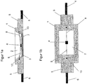
- FIG. 1a is a cross-section of a schematic representation of an embodiment of an LED housing shown.
- the LED housing 1 has a housing cavity 2. Within the housing cavity 2 is a Carrier element 3, on whose one upper side an LED chip 4 is arranged. On the side opposite the top side, a heat-conducting element 7 is arranged.
- the LED housing 1 furthermore has holding elements 5 and housing connection elements 6, which are located on two outer sides of the LED housing 1.
- the housing connection elements 6 in turn have an electrical connection 8 to the LED chip 4, wherein a bonding connection 13, the electrical connection 8, for example, realized by means of bonding wire, connects to the housing connection element 6.
- each holding element 5 may be formed as part of the LED housing 1, or be attached as a separate element on the LED housing 1 during a manufacturing process.
- FIG. 1b is a top view of the in FIG. 1a shown LED housing 1 shown.
- the LED housing is both electrically and mechanically mountable by SMT.
- the housing connection elements are connected to a drive circuit by means of soldering methods.
- a counterpart, not shown, can be connected to the retaining element 5 and the housing connecting element 6 by suitable shaping, wherein the retaining element 5 generates additional retaining force.
- the Housing connection elements of the same LED housing 1 are connected to each other by means of this counterpart.
- the heat dissipation element 7 is used in particular for high-power LEDs for improved heat dissipation from the interior of the LED housing 1 and protects the LED chip 4 from overheating and destruction.
- the LED housing 1 is mounted on a heat sink, whereby the heat dissipation can be significantly improved.
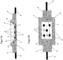
- FIG. 2 shows a further education in FIG. 1 illustrated embodiment of the LED housing.
- the structure is in principle comparable to the embodiment of FIG. 1 , which here only on the differences to the FIG. 1 pointed embodiment is received.
- a series connection of a plurality of LED chips 4 is introduced into the housing cavity 2.
- the housing connection element 6 has an electrical connection 8 to one of the LED chips 4, wherein the LED chips 4 are interconnected in series.
- all the anode terminals of an LED chip 4 are connected to a cathode terminal of the next LED chip 4 located in the cavity 2 by means of bond interconnection 9. Only the anode terminal of the first LED chip 4 of the series circuit and the cathode terminal of the last LED chip 4 of the series circuit are not connected, but each electrically connected to the housing connection elements 6 by means of bond 13.
- FIG. 2b An explanation of the series connection of the LED chips 4 is in FIG. 2b demonstrated.
- the LED chips 4 are shown schematically with two terminals, an anode and a cathode connection, wherein in each case a cathode connection to the anode terminal of an adjacent LED chip by means of Bond interconnect 9 is connected.
- the first anode terminal and the last cathode terminal are each connected to a housing terminal element 6. This again takes place via electrical connections 8 and the bond connection 13.
- the advantage of this development is an increase in the luminous intensity of an LED housing 1 in general. By a plurality of LED chips 4, a multiplication of the emitted light intensity is possible. A driving of the series-connected LED chips 4 takes place here again via the housing connection elements 6. Comparable with the embodiment of FIG. 1 have the holding elements 5 in connection with the housing connection elements 6 several ways to mount the LED housing 1.
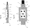
- FIG. 3 is an alternative embodiment to the in FIG. 1 shown embodiment of the LED housing shown. Due to the strong similarity to those already described FIGS. 1 and 2 Here, only the characteristic differences to these figures are discussed. Unlike in FIG. 1 The housing connector 6 now has two different shapes, each mold being a special type of connector. In this case, the first anode connection 8a is electrically connected to an anode connection element 6a and the last cathode connection is electrically connected to a cathode connection element 6b.
- the anode connection element 6a has the function of a plug and the cathode connection element 6b in this case the Function of a socket on.
- this plug-in system is standardized and corresponds to a standard.
- this LED housing can be easily integrated into an existing connector system, for example in the automotive, electronics or equipment sector. Because the retaining element is already made part of the housing, no additional counterpart or additional mount is required and the LED housing can be used universally. This saves additional costs and bypasses any transitional losses that are always present in adapters.
- Comparable to FIG. 1 and 2 is a sufficient heat dissipation, especially for high-power LEDs, achieved by the heat dissipation element 7.
- a corresponding electrical and / or mechanical connection to the connecting elements 6a and 6b can in turn be carried out preferably standardized via plug-in systems, locking systems or screw systems.
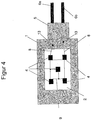
- FIG. 4 is a further education of in FIG. 3 shown embodiment of the LED housing shown, in which case the sectional view is omitted.
- the following is again only compared to the differences FIG. 3 received.
- one holding element 5 is shown, which serves to connect a plurality of LED housings or to a carrier.
- a plug for example, is the illustrated Embodiment with a carrier electrically contacted but also with other LED housings 1 connectable.
- cathode terminal and anode terminal members 6a and 6b are formed separately.
- this variant is used for mounting in a perforated circuit board, or mounted on a support or plugged.
- FIG. 5 shows four developments of an alternative embodiment of in FIG. 1 illustrated embodiment of the LED housing as 3D sketches.
- the holding element may for example be designed in several parts.
- the holding elements 5 in FIG. 5a are for example screw mounts and plug mating piece.
- a mechanical holding force with a carrier is made possible, but also a holding force of a tailor-made counterpart, not shown, of the housing connecting element for an electrically conductive connection.
- the LED housing 1 in FIG. 5a an optical element 15, which serves for beam deflection of the emitted electromagnetic radiation here of each LED chip 4.
- an optimal emission characteristic for the respective LED housing is achieved with respect to the respective application.
- connecting elements 14 in this case screws are provided. These serve primarily the mechanical connection with a carrier, in particular a heat sink. Other connecting elements are also conceivable and not excluded from the inventive idea.
- FIGS. 5b to 5d basically have similar elements. Different is, for example, the shape of the optical element, which in FIGS. 5c and 5d as an element for all LED chips 4 is executed. Furthermore, the housing connection elements 6, 6a, 6b are designed differently, wherein in FIG. 5d an already mentioned standardized electrical connection, for example, for the automotive sector, is provided. On the other hand is in FIG. 5c a variant for an alternative system recognizable.
- the indicated holes in the FIGS. 5a to 5d are here holding elements 5 and make it clear that the holding element 5 is very easy to produce as part of the LED housing 1.
- the holding element may consist of several parts, wherein a part of the holders are fastened by means of screw connection to a carrier.
- the holding element 5 may have other parts 5 for secure connection to another LED housing or a circuit board or a heat sink.
- FIG. 2 shows embodiment of the LED housing shown. Different from FIG. 2 Here is that each LED can be individually controlled.
- FIG. 6c this shows a variant in which each holding element 5 has a cathode connection element 6b and anode connection element 6a.
- FIG. 7 will be further education in FIG. 6 shown embodiment of the LED housing shown.
- the LED chips 4 in FIG. 7 an unillustrated control, which can be controlled via a control connection element 10 and a control connection connection 11.
- each LED chip individually, preferably the intensity of the electromagnetic light to be emitted.
- control connection elements 10 like the holding elements 5 and housing connection elements 6, 6a and 6b, can be freely designed in their shape and standardized in a preferred manner in order to permit flexible and rapid expansion with other LED housings, electrical connection or activation. The same applies to the installation variants with a carrier.
- connection of the LED chips 4 Figure 1 to 7 between them is preferably carried out by means of bond interconnection, wherein the carrier element may additionally also have not shown conductor structures.
- a connection of the connecting elements 6, 6a and 6b with the respective LED chip terminals 8, 8a and 8b is preferably carried out by means of laser welding or classical Wirebondvon.
- a support member 3 is preferably a DBC ceramic substrate to use, since it acts by its special "sandwich structure" (copper - ceramic - copper) electrically insulating and allowing laterally spread heat removal, which makes this substrate a good thermal conductor.
- the LED chip sides, with which the LED chip 4 is mounted on the support member 3 be designed to be electrically insulating.
- the LED housing As a material for the LED housing are primarily plastics, such as PPA, LCP, PEEK or PEI to use.
- the carrier element is in particular a DBC, MKP-PCB or AIN ceramic substrate.
- metallic supports such as copper or copper alloy with bonding metallization applicable.
- the LED chip backs In the case of a non-insulating carrier, the LED chip backs must be insulating.
- Another object of the retaining element 5 is the function as a spacer for the use of a common carrier by two identical LED housing. In this case, it is important that there is enough space between the individual LED housings to ensure sufficient heat dissipation.
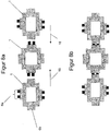
- FIG. 8 shows now a series connection of three plugged together LED housings 1.
- the LED housing 1 are according to one of the embodiments and / or developments of FIGS. 1-7 designed. They have both a cathode connection element 6b and a Anodenan gleichelement 6a and are in a Georgiasteck compiler 16, as in FIG. 8b shown, connected.
- the LED chips not shown here are covered by one of the in Figure 1 to 7 connected variant embodiments and electrically and / or mechanically linked by means of anode connection element 6a or cathode connection element 6b.
- an assembly on a support by means of further described holding elements 5 is also conceivable beyond.
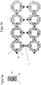
- FIG. 9 shows an alternative interconnection of individual LED housing 1, shown here is a parallel circuit of four series-connected LED housings 1.
- the LED housing 1 correspond to one of the previously described embodiments and / or developmentssformen.
- Characteristic of a parallel connection is the connection of two anode connection elements 6a, which is made possible with an adapter piece 17 according to the invention.
- the adapter piece 17 is in FIG. 9a A further object of the adapter piece 17 is the function as a spacer or spacers for better heat dissipation, if a common heat sink is used for the interconnected LED housing.
- FIG. 10 a further alternative interconnection of the described LED housing 1 is shown.
- each LED package has a plurality of package terminal members 6a and 6b, whereby each individual package connector 6a and 6b has an LED chip 4 inside the package cavity 2 of each LED housing 1 controls.
- each LED housing 1 on LED chips 4, not shown.
- a bridge adapter 19 is shown in FIG FIG. 10a which in turn represents only a bridging 20 of two connection elements 6a and 6b. It is a fitting counterpart of the housing connection element 6a or 6b of each side of an LED housing 1 and has an anode connection element 6a and a cathode connection element 6b.
- FIG. 10a illustrated bridge adapter for bridging the cathode with the anode terminal of the LED to be operated.
- bridge adapter for bridging the cathode with the anode terminal of the LED to be operated.
- the operation of the LED chips 4 and the supply of power to each chip 4 to be operated is adapted to the respective interconnection by means of current driver circuits.
- These current driver circuits regulate an always constant and necessary for operation operating current. It is conceivable to add and remove LED housings 1 during operation, whereby a short circuit or overload scenario by the current driver circuits must be taken into account and eliminated accordingly.
Landscapes
- Engineering & Computer Science (AREA)
- Microelectronics & Electronic Packaging (AREA)
- Physics & Mathematics (AREA)
- General Engineering & Computer Science (AREA)
- Power Engineering (AREA)
- Optics & Photonics (AREA)
- Condensed Matter Physics & Semiconductors (AREA)
- General Physics & Mathematics (AREA)
- Computer Hardware Design (AREA)
- Led Device Packages (AREA)
- Arrangement Of Elements, Cooling, Sealing, Or The Like Of Lighting Devices (AREA)
- Fastening Of Light Sources Or Lamp Holders (AREA)
Applications Claiming Priority (2)
| Application Number | Priority Date | Filing Date | Title |
|---|---|---|---|
| DE102007041136A DE102007041136A1 (de) | 2007-08-30 | 2007-08-30 | LED-Gehäuse |
| PCT/DE2008/001293 WO2009026876A1 (de) | 2007-08-30 | 2008-08-06 | Led-gehäuse |
Publications (2)
| Publication Number | Publication Date |
|---|---|
| EP2183794A1 EP2183794A1 (de) | 2010-05-12 |
| EP2183794B1 true EP2183794B1 (de) | 2017-04-05 |
Family
ID=40085583
Family Applications (1)
| Application Number | Title | Priority Date | Filing Date |
|---|---|---|---|
| EP08801127.5A Not-in-force EP2183794B1 (de) | 2007-08-30 | 2008-08-06 | Led-gehäuse |
Country Status (8)
| Country | Link |
|---|---|
| US (1) | US8487323B2 (enExample) |
| EP (1) | EP2183794B1 (enExample) |
| JP (1) | JP2010537437A (enExample) |
| KR (1) | KR20100047339A (enExample) |
| CN (2) | CN102664219B (enExample) |
| DE (1) | DE102007041136A1 (enExample) |
| TW (1) | TW200917533A (enExample) |
| WO (1) | WO2009026876A1 (enExample) |
Families Citing this family (36)
| Publication number | Priority date | Publication date | Assignee | Title |
|---|---|---|---|---|
| US9070850B2 (en) | 2007-10-31 | 2015-06-30 | Cree, Inc. | Light emitting diode package and method for fabricating same |
| US7675145B2 (en) * | 2006-03-28 | 2010-03-09 | Cree Hong Kong Limited | Apparatus, system and method for use in mounting electronic elements |
| US8748915B2 (en) * | 2006-04-24 | 2014-06-10 | Cree Hong Kong Limited | Emitter package with angled or vertical LED |
| US8735920B2 (en) | 2006-07-31 | 2014-05-27 | Cree, Inc. | Light emitting diode package with optical element |
| US9711703B2 (en) | 2007-02-12 | 2017-07-18 | Cree Huizhou Opto Limited | Apparatus, system and method for use in mounting electronic elements |
| CN101388161A (zh) * | 2007-09-14 | 2009-03-18 | 科锐香港有限公司 | Led表面安装装置和并入有此装置的led显示器 |
| US8866169B2 (en) | 2007-10-31 | 2014-10-21 | Cree, Inc. | LED package with increased feature sizes |
| US10256385B2 (en) | 2007-10-31 | 2019-04-09 | Cree, Inc. | Light emitting die (LED) packages and related methods |
| US8791471B2 (en) * | 2008-11-07 | 2014-07-29 | Cree Hong Kong Limited | Multi-chip light emitting diode modules |
| US20110037083A1 (en) * | 2009-01-14 | 2011-02-17 | Alex Chi Keung Chan | Led package with contrasting face |
| US8368112B2 (en) | 2009-01-14 | 2013-02-05 | Cree Huizhou Opto Limited | Aligned multiple emitter package |
| US7956546B2 (en) * | 2009-05-15 | 2011-06-07 | Bridgelux, Inc. | Modular LED light bulb |
| EP2556288B1 (de) * | 2010-04-09 | 2015-06-10 | Tridonic Dresden GmbH & Co. KG | Leuchtmodul und leuchte |
| KR101543333B1 (ko) | 2010-04-23 | 2015-08-11 | 삼성전자주식회사 | 발광소자 패키지용 리드 프레임, 발광소자 패키지, 및 발광소자 패키지를 채용한 조명장치 |
| DE102010038252A1 (de) * | 2010-10-18 | 2012-04-19 | Koninklijke Philips Electronics N.V. | Fassung für eine Leuchte mit OLED-Leuchtmittel |
| DE102010038251A1 (de) | 2010-10-18 | 2012-04-19 | Koninklijke Philips Electronics N.V. | OLED-Leuchtmittel für eine Leuchte |
| US9285089B2 (en) * | 2010-12-21 | 2016-03-15 | Bridgelux, Inc. | Automatic electrical connection assembly for light modules |
| JP5841802B2 (ja) * | 2011-10-24 | 2016-01-13 | パナソニックIpマネジメント株式会社 | 照明器具 |
| US8564004B2 (en) * | 2011-11-29 | 2013-10-22 | Cree, Inc. | Complex primary optics with intermediate elements |
| US8759847B2 (en) * | 2011-12-22 | 2014-06-24 | Bridgelux, Inc. | White LED assembly with LED string and intermediate node substrate terminals |
| US20130175704A1 (en) * | 2012-01-05 | 2013-07-11 | Ixys Corporation | Discrete power transistor package having solderless dbc to leadframe attach |
| KR101933189B1 (ko) | 2012-01-31 | 2019-04-05 | 서울반도체 주식회사 | 발광다이오드 패키지 |
| CN102937270B (zh) * | 2012-11-23 | 2015-01-21 | 昆山博爱模具开发有限公司 | 一种led壳体 |
| CN103236483A (zh) * | 2013-03-15 | 2013-08-07 | 达亮电子(苏州)有限公司 | 发光二极管封装结构及封装方法 |
| TWI598665B (zh) * | 2013-03-15 | 2017-09-11 | 隆達電子股份有限公司 | 發光元件、長條狀發光元件及其應用 |
| DE102013226721A1 (de) | 2013-12-19 | 2015-06-25 | Osram Opto Semiconductors Gmbh | Optoelektronisches Bauelement mit asymmetrischen Trägerarmen |
| CH709337B1 (fr) * | 2014-03-04 | 2016-12-30 | Robert Alderton | Unité d'éclairage LED et procédé de fabrication d'une telle unité. |
| JP6190746B2 (ja) * | 2014-03-25 | 2017-08-30 | エムテックスマツムラ株式会社 | 半導体素子実装用中空パッケージ |
| US9601670B2 (en) | 2014-07-11 | 2017-03-21 | Cree, Inc. | Method to form primary optic with variable shapes and/or geometries without a substrate |
| KR102233038B1 (ko) | 2014-07-30 | 2021-03-30 | 엘지이노텍 주식회사 | 광원 모듈 |
| US10622522B2 (en) | 2014-09-05 | 2020-04-14 | Theodore Lowes | LED packages with chips having insulated surfaces |
| JP6484588B2 (ja) | 2016-05-19 | 2019-03-13 | 日亜化学工業株式会社 | 発光装置及び発光装置用パッケージ |
| JP6880725B2 (ja) * | 2016-12-27 | 2021-06-02 | 日亜化学工業株式会社 | 発光装置 |
| RU172080U1 (ru) * | 2017-01-09 | 2017-06-28 | федеральное государственное бюджетное образовательное учреждение высшего образования "Новгородский государственный университет имени Ярослава Мудрого" | Корпус светодиода для поверхностного монтажа |
| CN108879242B (zh) * | 2017-05-12 | 2022-03-29 | 中兴通讯股份有限公司 | 传输线及其发光线缆 |
| DE102018214059A1 (de) * | 2018-08-21 | 2020-02-27 | Robert Bosch Gmbh | Gehäuserahmen für ein Steuergerät, welcher zur elektrischen Außenkontaktierung eines Schaltungsträgers des Steuergeräts geeignet ist |
Family Cites Families (36)
| Publication number | Priority date | Publication date | Assignee | Title |
|---|---|---|---|---|
| JPS5610983A (en) * | 1979-07-06 | 1981-02-03 | Mitsubishi Electric Corp | Composite semiconductor device |
| DE2927534A1 (de) | 1979-07-07 | 1981-01-08 | Bayer Ag | Optisch reine heterocyclische aminosaeuren, verfahren zu ihrer herstellung und ihre verwendung |
| JPS5612368U (enExample) * | 1979-07-10 | 1981-02-02 | ||
| US4423465A (en) * | 1981-09-30 | 1983-12-27 | Teng Ching Weng | Combination electronic circuit element with multidirectionally adjustable joints |
| JPS6153807A (ja) | 1984-08-23 | 1986-03-17 | Toshiba Corp | 電流源回路 |
| JPS6346971Y2 (enExample) * | 1984-09-13 | 1988-12-05 | ||
| JPS61195076A (ja) | 1985-02-25 | 1986-08-29 | Nec Corp | フアクシミリ送信機 |
| JPH083024Y2 (ja) * | 1985-05-27 | 1996-01-29 | タキロン株式会社 | 発光体素子保持ブロック |
| US4667277A (en) * | 1985-09-20 | 1987-05-19 | General Instrument Corporation | Indicator lamp assembly |
| JPS63138537A (ja) | 1986-11-29 | 1988-06-10 | Toshiba Corp | 発光装置 |
| DE19818402A1 (de) | 1998-04-24 | 1999-10-28 | Horn Hannes Schulze | Einrichtung für Beleuchtungszwecke |
| DE19853424A1 (de) | 1998-10-27 | 2000-06-08 | Friedrich Hans Josef | Leuchtdiode mit besonderen Fähigkeiten / Baustein - Leuchtdiode |
| JP3743186B2 (ja) * | 1998-12-15 | 2006-02-08 | 松下電工株式会社 | 発光ダイオード |
| JP2001168400A (ja) * | 1999-12-09 | 2001-06-22 | Rohm Co Ltd | ケース付チップ型発光装置およびその製造方法 |
| DE10012734C1 (de) | 2000-03-16 | 2001-09-27 | Bjb Gmbh & Co Kg | Illuminationsbausatz für Beleuchtungs-, Anzeige- oder Hinweiszwecke sowie Steckverbinder für einen solchen Illuminationsbausatz |
| JP2003179264A (ja) * | 2001-12-10 | 2003-06-27 | Nobuyoshi Imashiro | Ledの連続接続コネクタおよびその製造方法 |
| JP3912607B2 (ja) * | 2002-06-19 | 2007-05-09 | サンケン電気株式会社 | 半導体発光装置の製法 |
| DE10242292A1 (de) | 2002-09-12 | 2004-04-01 | Sebastian Matthias | Flächenlampe |
| US6911731B2 (en) * | 2003-05-14 | 2005-06-28 | Jiahn-Chang Wu | Solderless connection in LED module |
| US7458705B2 (en) * | 2003-06-20 | 2008-12-02 | Yazaki Corporation | LED illumination device |
| DE10331574A1 (de) * | 2003-07-11 | 2005-02-17 | eupec Europäische Gesellschaft für Leistungshalbleiter mbH | Leistungshalbleitermodul |
| DE20311557U1 (de) * | 2003-07-26 | 2003-10-16 | Neuhorst Paul Heinrich | Leuchte für Beleuchtungszwecke |
| JP4711715B2 (ja) | 2005-03-30 | 2011-06-29 | 株式会社東芝 | 半導体発光装置及び半導体発光ユニット |
| US20060262533A1 (en) * | 2005-05-18 | 2006-11-23 | Para Light Electronics Co., Ltd. | Modular light emitting diode |
| JP2006344420A (ja) | 2005-06-07 | 2006-12-21 | Alps Electric Co Ltd | Ledランプモジュール |
| US7230222B2 (en) | 2005-08-15 | 2007-06-12 | Avago Technologies Ecbu Ip (Singapore) Pte. Ltd. | Calibrated LED light module |
| DE602006020486D1 (de) | 2005-12-16 | 2011-04-14 | Koninkl Philips Electronics Nv | Miteinander verbindbare beleuchtungsmodule umfassendes beleuchtungssystem |
| JP2007208203A (ja) | 2006-02-06 | 2007-08-16 | Matsushita Electric Ind Co Ltd | 発光光源及び発光システム |
| US20070184722A1 (en) * | 2006-02-07 | 2007-08-09 | Dynatech Action, Inc. | Powered modular building block toy |
| JP2007213881A (ja) | 2006-02-08 | 2007-08-23 | Aristo Engineering Pte Ltd | 照明装置ユニット、照明装置及び照明装置機構 |
| DE102006018668B4 (de) * | 2006-04-21 | 2013-04-11 | Osram Gmbh | Modulares Beleuchtungssystem und Beleuchtungsanordnung |
| US7880283B2 (en) * | 2006-04-25 | 2011-02-01 | International Rectifier Corporation | High reliability power module |
| KR100735432B1 (ko) * | 2006-05-18 | 2007-07-04 | 삼성전기주식회사 | 발광소자 패키지 및 발광소자 패키지 어레이 |
| JP2008159394A (ja) | 2006-12-22 | 2008-07-10 | Koha Co Ltd | 取付けユニットおよび面状発光装置 |
| US7442070B2 (en) * | 2007-02-15 | 2008-10-28 | Super Link Electronics Co., Ltd. | Light-emitting cell module |
| US7633055B2 (en) * | 2007-03-08 | 2009-12-15 | Lumination Llc | Sealed light emitting diode assemblies including annular gaskets and methods of making same |
-
2007
- 2007-08-30 DE DE102007041136A patent/DE102007041136A1/de not_active Withdrawn
-
2008
- 2008-08-06 KR KR1020107006731A patent/KR20100047339A/ko not_active Ceased
- 2008-08-06 US US12/675,009 patent/US8487323B2/en not_active Expired - Fee Related
- 2008-08-06 CN CN201210124304.XA patent/CN102664219B/zh not_active Expired - Fee Related
- 2008-08-06 JP JP2010522178A patent/JP2010537437A/ja active Pending
- 2008-08-06 CN CN2008801045110A patent/CN101790802B/zh not_active Expired - Fee Related
- 2008-08-06 EP EP08801127.5A patent/EP2183794B1/de not_active Not-in-force
- 2008-08-06 WO PCT/DE2008/001293 patent/WO2009026876A1/de not_active Ceased
- 2008-08-18 TW TW097131402A patent/TW200917533A/zh unknown
Non-Patent Citations (1)
| Title |
|---|
| None * |
Also Published As
| Publication number | Publication date |
|---|---|
| US20110186880A1 (en) | 2011-08-04 |
| TW200917533A (en) | 2009-04-16 |
| EP2183794A1 (de) | 2010-05-12 |
| KR20100047339A (ko) | 2010-05-07 |
| CN101790802B (zh) | 2012-06-20 |
| JP2010537437A (ja) | 2010-12-02 |
| CN102664219A (zh) | 2012-09-12 |
| DE102007041136A1 (de) | 2009-03-05 |
| US8487323B2 (en) | 2013-07-16 |
| CN102664219B (zh) | 2016-07-06 |
| CN101790802A (zh) | 2010-07-28 |
| WO2009026876A1 (de) | 2009-03-05 |
Similar Documents
| Publication | Publication Date | Title |
|---|---|---|
| EP2183794B1 (de) | Led-gehäuse | |
| DE112006000920B4 (de) | LED-Einheit und LED-Beleuchtungslampe, die die LED-Einheit verwendet | |
| EP2198196B1 (de) | Lampe | |
| EP3167224B1 (de) | Halbleiterlampe | |
| DE102007059133B4 (de) | Substrat für ein LED-Submount, LED-Submount und LED-Lichtquelle | |
| DE102014109718B4 (de) | Licht emittierende Vorrichtung und Beleuchtungseinrichtung unter Verwendung derselben | |
| EP2815177B1 (de) | Leuchtmodul | |
| DE102010030702A1 (de) | Halbleiterlampe | |
| WO2013135527A1 (de) | Leuchtdiodenlampe und verfahren zum fertigen einer leuchtdiodenlampe | |
| DE102005014144A1 (de) | Leuchtdiode | |
| EP2347639A1 (de) | Beleuchtungsvorrichtung mit zwei leiterplatten | |
| WO2016091432A1 (de) | Lampe mit treiberplatine und sockel | |
| DE102006032416A1 (de) | Strahlungsemittierendes Bauelement | |
| EP2938170A1 (de) | Halter für SMD-Leuchtdiode | |
| EP2613079A1 (de) | LED-Leuchtmittel | |
| WO2015007904A1 (de) | Leuchtvorrichtung mit halbleiterlichtquelle und treiberplatine | |
| DE10230105B4 (de) | Weiße LED-Lichtquelle | |
| WO2009115063A1 (de) | Anordnung, lampenanordnung und verfahren zum emittieren von licht | |
| DE102009033915A1 (de) | Verfahren zur Herstellung eines Leuchtmittels und Leuchtmittel | |
| DE102006009812B4 (de) | Montageanordnung für mehrere Leistungshalbleiter und Schaltung mit einer solchen Montageanordnung | |
| EP2191192A2 (de) | Elektrische leuchte mit einer leuchtdiode und einem leuchten-reflektor | |
| EP2927564B1 (de) | Leuchteinrichtung für leuchtmittel | |
| DE102010018253A1 (de) | Lichtquellenmodul und Lichtquelle | |
| EP2845235B1 (de) | Led-anordnung | |
| DE102004031685A1 (de) | Gehäuse für ein optoelektronisches Bauelement und optoelektronisches Bauelement |
Legal Events
| Date | Code | Title | Description |
|---|---|---|---|
| PUAI | Public reference made under article 153(3) epc to a published international application that has entered the european phase |
Free format text: ORIGINAL CODE: 0009012 |
|
| 17P | Request for examination filed |
Effective date: 20100120 |
|
| AK | Designated contracting states |
Kind code of ref document: A1 Designated state(s): AT BE BG CH CY CZ DE DK EE ES FI FR GB GR HR HU IE IS IT LI LT LU LV MC MT NL NO PL PT RO SE SI SK TR |
|
| AX | Request for extension of the european patent |
Extension state: AL BA MK RS |
|
| DAX | Request for extension of the european patent (deleted) | ||
| GRAP | Despatch of communication of intention to grant a patent |
Free format text: ORIGINAL CODE: EPIDOSNIGR1 |
|
| INTG | Intention to grant announced |
Effective date: 20161124 |
|
| GRAS | Grant fee paid |
Free format text: ORIGINAL CODE: EPIDOSNIGR3 |
|
| GRAA | (expected) grant |
Free format text: ORIGINAL CODE: 0009210 |
|
| AK | Designated contracting states |
Kind code of ref document: B1 Designated state(s): AT BE BG CH CY CZ DE DK EE ES FI FR GB GR HR HU IE IS IT LI LT LU LV MC MT NL NO PL PT RO SE SI SK TR |
|
| REG | Reference to a national code |
Ref country code: GB Ref legal event code: FG4D Free format text: NOT ENGLISH |
|
| REG | Reference to a national code |
Ref country code: CH Ref legal event code: EP |
|
| REG | Reference to a national code |
Ref country code: AT Ref legal event code: REF Ref document number: 882544 Country of ref document: AT Kind code of ref document: T Effective date: 20170415 |
|
| REG | Reference to a national code |
Ref country code: IE Ref legal event code: FG4D Free format text: LANGUAGE OF EP DOCUMENT: GERMAN |
|
| REG | Reference to a national code |
Ref country code: DE Ref legal event code: R096 Ref document number: 502008015196 Country of ref document: DE |
|
| REG | Reference to a national code |
Ref country code: NL Ref legal event code: MP Effective date: 20170405 |
|
| REG | Reference to a national code |
Ref country code: LT Ref legal event code: MG4D |
|
| PG25 | Lapsed in a contracting state [announced via postgrant information from national office to epo] |
Ref country code: NL Free format text: LAPSE BECAUSE OF FAILURE TO SUBMIT A TRANSLATION OF THE DESCRIPTION OR TO PAY THE FEE WITHIN THE PRESCRIBED TIME-LIMIT Effective date: 20170405 |
|
| PG25 | Lapsed in a contracting state [announced via postgrant information from national office to epo] |
Ref country code: GR Free format text: LAPSE BECAUSE OF FAILURE TO SUBMIT A TRANSLATION OF THE DESCRIPTION OR TO PAY THE FEE WITHIN THE PRESCRIBED TIME-LIMIT Effective date: 20170706 Ref country code: FI Free format text: LAPSE BECAUSE OF FAILURE TO SUBMIT A TRANSLATION OF THE DESCRIPTION OR TO PAY THE FEE WITHIN THE PRESCRIBED TIME-LIMIT Effective date: 20170405 Ref country code: LT Free format text: LAPSE BECAUSE OF FAILURE TO SUBMIT A TRANSLATION OF THE DESCRIPTION OR TO PAY THE FEE WITHIN THE PRESCRIBED TIME-LIMIT Effective date: 20170405 Ref country code: ES Free format text: LAPSE BECAUSE OF FAILURE TO SUBMIT A TRANSLATION OF THE DESCRIPTION OR TO PAY THE FEE WITHIN THE PRESCRIBED TIME-LIMIT Effective date: 20170405 Ref country code: NO Free format text: LAPSE BECAUSE OF FAILURE TO SUBMIT A TRANSLATION OF THE DESCRIPTION OR TO PAY THE FEE WITHIN THE PRESCRIBED TIME-LIMIT Effective date: 20170705 Ref country code: HR Free format text: LAPSE BECAUSE OF FAILURE TO SUBMIT A TRANSLATION OF THE DESCRIPTION OR TO PAY THE FEE WITHIN THE PRESCRIBED TIME-LIMIT Effective date: 20170405 |
|
| PG25 | Lapsed in a contracting state [announced via postgrant information from national office to epo] |
Ref country code: BG Free format text: LAPSE BECAUSE OF FAILURE TO SUBMIT A TRANSLATION OF THE DESCRIPTION OR TO PAY THE FEE WITHIN THE PRESCRIBED TIME-LIMIT Effective date: 20170705 Ref country code: SE Free format text: LAPSE BECAUSE OF FAILURE TO SUBMIT A TRANSLATION OF THE DESCRIPTION OR TO PAY THE FEE WITHIN THE PRESCRIBED TIME-LIMIT Effective date: 20170405 Ref country code: IS Free format text: LAPSE BECAUSE OF FAILURE TO SUBMIT A TRANSLATION OF THE DESCRIPTION OR TO PAY THE FEE WITHIN THE PRESCRIBED TIME-LIMIT Effective date: 20170805 Ref country code: PL Free format text: LAPSE BECAUSE OF FAILURE TO SUBMIT A TRANSLATION OF THE DESCRIPTION OR TO PAY THE FEE WITHIN THE PRESCRIBED TIME-LIMIT Effective date: 20170405 Ref country code: LV Free format text: LAPSE BECAUSE OF FAILURE TO SUBMIT A TRANSLATION OF THE DESCRIPTION OR TO PAY THE FEE WITHIN THE PRESCRIBED TIME-LIMIT Effective date: 20170405 |
|
| REG | Reference to a national code |
Ref country code: DE Ref legal event code: R097 Ref document number: 502008015196 Country of ref document: DE |
|
| PG25 | Lapsed in a contracting state [announced via postgrant information from national office to epo] |
Ref country code: DK Free format text: LAPSE BECAUSE OF FAILURE TO SUBMIT A TRANSLATION OF THE DESCRIPTION OR TO PAY THE FEE WITHIN THE PRESCRIBED TIME-LIMIT Effective date: 20170405 Ref country code: SK Free format text: LAPSE BECAUSE OF FAILURE TO SUBMIT A TRANSLATION OF THE DESCRIPTION OR TO PAY THE FEE WITHIN THE PRESCRIBED TIME-LIMIT Effective date: 20170405 Ref country code: EE Free format text: LAPSE BECAUSE OF FAILURE TO SUBMIT A TRANSLATION OF THE DESCRIPTION OR TO PAY THE FEE WITHIN THE PRESCRIBED TIME-LIMIT Effective date: 20170405 Ref country code: RO Free format text: LAPSE BECAUSE OF FAILURE TO SUBMIT A TRANSLATION OF THE DESCRIPTION OR TO PAY THE FEE WITHIN THE PRESCRIBED TIME-LIMIT Effective date: 20170405 Ref country code: CZ Free format text: LAPSE BECAUSE OF FAILURE TO SUBMIT A TRANSLATION OF THE DESCRIPTION OR TO PAY THE FEE WITHIN THE PRESCRIBED TIME-LIMIT Effective date: 20170405 |
|
| PLBE | No opposition filed within time limit |
Free format text: ORIGINAL CODE: 0009261 |
|
| STAA | Information on the status of an ep patent application or granted ep patent |
Free format text: STATUS: NO OPPOSITION FILED WITHIN TIME LIMIT |
|
| PG25 | Lapsed in a contracting state [announced via postgrant information from national office to epo] |
Ref country code: IT Free format text: LAPSE BECAUSE OF FAILURE TO SUBMIT A TRANSLATION OF THE DESCRIPTION OR TO PAY THE FEE WITHIN THE PRESCRIBED TIME-LIMIT Effective date: 20170405 |
|
| 26N | No opposition filed |
Effective date: 20180108 |
|
| REG | Reference to a national code |
Ref country code: CH Ref legal event code: PL |
|
| PG25 | Lapsed in a contracting state [announced via postgrant information from national office to epo] |
Ref country code: MC Free format text: LAPSE BECAUSE OF FAILURE TO SUBMIT A TRANSLATION OF THE DESCRIPTION OR TO PAY THE FEE WITHIN THE PRESCRIBED TIME-LIMIT Effective date: 20170405 |
|
| GBPC | Gb: european patent ceased through non-payment of renewal fee |
Effective date: 20170806 |
|
| PG25 | Lapsed in a contracting state [announced via postgrant information from national office to epo] |
Ref country code: LI Free format text: LAPSE BECAUSE OF NON-PAYMENT OF DUE FEES Effective date: 20170831 Ref country code: CH Free format text: LAPSE BECAUSE OF NON-PAYMENT OF DUE FEES Effective date: 20170831 |
|
| REG | Reference to a national code |
Ref country code: FR Ref legal event code: ST Effective date: 20180430 |
|
| REG | Reference to a national code |
Ref country code: IE Ref legal event code: MM4A |
|
| PG25 | Lapsed in a contracting state [announced via postgrant information from national office to epo] |
Ref country code: SI Free format text: LAPSE BECAUSE OF FAILURE TO SUBMIT A TRANSLATION OF THE DESCRIPTION OR TO PAY THE FEE WITHIN THE PRESCRIBED TIME-LIMIT Effective date: 20170405 |
|
| REG | Reference to a national code |
Ref country code: BE Ref legal event code: MM Effective date: 20170831 |
|
| PG25 | Lapsed in a contracting state [announced via postgrant information from national office to epo] |
Ref country code: LU Free format text: LAPSE BECAUSE OF NON-PAYMENT OF DUE FEES Effective date: 20170806 |
|
| PG25 | Lapsed in a contracting state [announced via postgrant information from national office to epo] |
Ref country code: GB Free format text: LAPSE BECAUSE OF NON-PAYMENT OF DUE FEES Effective date: 20170806 Ref country code: IE Free format text: LAPSE BECAUSE OF NON-PAYMENT OF DUE FEES Effective date: 20170806 |
|
| PG25 | Lapsed in a contracting state [announced via postgrant information from national office to epo] |
Ref country code: FR Free format text: LAPSE BECAUSE OF NON-PAYMENT OF DUE FEES Effective date: 20170831 Ref country code: BE Free format text: LAPSE BECAUSE OF NON-PAYMENT OF DUE FEES Effective date: 20170831 |
|
| PG25 | Lapsed in a contracting state [announced via postgrant information from national office to epo] |
Ref country code: MT Free format text: LAPSE BECAUSE OF FAILURE TO SUBMIT A TRANSLATION OF THE DESCRIPTION OR TO PAY THE FEE WITHIN THE PRESCRIBED TIME-LIMIT Effective date: 20170405 |
|
| REG | Reference to a national code |
Ref country code: AT Ref legal event code: MM01 Ref document number: 882544 Country of ref document: AT Kind code of ref document: T Effective date: 20170806 |
|
| PGFP | Annual fee paid to national office [announced via postgrant information from national office to epo] |
Ref country code: DE Payment date: 20180823 Year of fee payment: 11 |
|
| PG25 | Lapsed in a contracting state [announced via postgrant information from national office to epo] |
Ref country code: AT Free format text: LAPSE BECAUSE OF NON-PAYMENT OF DUE FEES Effective date: 20170806 |
|
| PG25 | Lapsed in a contracting state [announced via postgrant information from national office to epo] |
Ref country code: HU Free format text: LAPSE BECAUSE OF FAILURE TO SUBMIT A TRANSLATION OF THE DESCRIPTION OR TO PAY THE FEE WITHIN THE PRESCRIBED TIME-LIMIT; INVALID AB INITIO Effective date: 20080806 |
|
| PG25 | Lapsed in a contracting state [announced via postgrant information from national office to epo] |
Ref country code: CY Free format text: LAPSE BECAUSE OF NON-PAYMENT OF DUE FEES Effective date: 20170405 |
|
| REG | Reference to a national code |
Ref country code: DE Ref legal event code: R119 Ref document number: 502008015196 Country of ref document: DE |
|
| PG25 | Lapsed in a contracting state [announced via postgrant information from national office to epo] |
Ref country code: TR Free format text: LAPSE BECAUSE OF FAILURE TO SUBMIT A TRANSLATION OF THE DESCRIPTION OR TO PAY THE FEE WITHIN THE PRESCRIBED TIME-LIMIT Effective date: 20170405 |
|
| PG25 | Lapsed in a contracting state [announced via postgrant information from national office to epo] |
Ref country code: PT Free format text: LAPSE BECAUSE OF FAILURE TO SUBMIT A TRANSLATION OF THE DESCRIPTION OR TO PAY THE FEE WITHIN THE PRESCRIBED TIME-LIMIT Effective date: 20170405 |
|
| PG25 | Lapsed in a contracting state [announced via postgrant information from national office to epo] |
Ref country code: DE Free format text: LAPSE BECAUSE OF NON-PAYMENT OF DUE FEES Effective date: 20200303 |