EP2179078B1 - Method and system for forming a silicon ingot using a low-grade silicon feedstock - Google Patents
Method and system for forming a silicon ingot using a low-grade silicon feedstock Download PDFInfo
- Publication number
- EP2179078B1 EP2179078B1 EP08796655A EP08796655A EP2179078B1 EP 2179078 B1 EP2179078 B1 EP 2179078B1 EP 08796655 A EP08796655 A EP 08796655A EP 08796655 A EP08796655 A EP 08796655A EP 2179078 B1 EP2179078 B1 EP 2179078B1
- Authority
- EP
- European Patent Office
- Prior art keywords
- silicon
- molten
- generally
- volume
- grade
- Prior art date
- Legal status (The legal status is an assumption and is not a legal conclusion. Google has not performed a legal analysis and makes no representation as to the accuracy of the status listed.)
- Not-in-force
Links
- XUIMIQQOPSSXEZ-UHFFFAOYSA-N Silicon Chemical compound [Si] XUIMIQQOPSSXEZ-UHFFFAOYSA-N 0.000 title claims abstract description 309
- 229910052710 silicon Inorganic materials 0.000 title claims abstract description 296
- 239000010703 silicon Substances 0.000 title claims abstract description 296
- 238000000034 method Methods 0.000 title claims abstract description 99
- 238000007711 solidification Methods 0.000 claims abstract description 30
- 230000008023 solidification Effects 0.000 claims abstract description 30
- 239000012535 impurity Substances 0.000 claims description 28
- 230000037361 pathway Effects 0.000 claims description 21
- 239000000463 material Substances 0.000 claims description 18
- 239000007789 gas Substances 0.000 claims description 14
- 238000002425 crystallisation Methods 0.000 claims description 9
- 230000008025 crystallization Effects 0.000 claims description 9
- 238000010438 heat treatment Methods 0.000 claims description 7
- 230000006911 nucleation Effects 0.000 claims description 7
- 238000010899 nucleation Methods 0.000 claims description 7
- 230000003750 conditioning effect Effects 0.000 claims description 6
- 238000000605 extraction Methods 0.000 claims description 6
- IJGRMHOSHXDMSA-UHFFFAOYSA-N Atomic nitrogen Chemical compound N#N IJGRMHOSHXDMSA-UHFFFAOYSA-N 0.000 claims description 4
- 230000007246 mechanism Effects 0.000 claims description 4
- 230000007847 structural defect Effects 0.000 claims description 4
- CURLTUGMZLYLDI-UHFFFAOYSA-N Carbon dioxide Chemical compound O=C=O CURLTUGMZLYLDI-UHFFFAOYSA-N 0.000 claims description 3
- 239000000654 additive Substances 0.000 claims description 3
- QVGXLLKOCUKJST-UHFFFAOYSA-N atomic oxygen Chemical compound [O] QVGXLLKOCUKJST-UHFFFAOYSA-N 0.000 claims description 3
- 239000001301 oxygen Substances 0.000 claims description 3
- 229910052760 oxygen Inorganic materials 0.000 claims description 3
- 230000009466 transformation Effects 0.000 claims description 3
- XLYOFNOQVPJJNP-UHFFFAOYSA-N water Chemical compound O XLYOFNOQVPJJNP-UHFFFAOYSA-N 0.000 claims description 3
- ZAMOUSCENKQFHK-UHFFFAOYSA-N Chlorine atom Chemical compound [Cl] ZAMOUSCENKQFHK-UHFFFAOYSA-N 0.000 claims description 2
- 230000000996 additive effect Effects 0.000 claims description 2
- 239000000460 chlorine Substances 0.000 claims description 2
- 229910052801 chlorine Inorganic materials 0.000 claims description 2
- 239000001257 hydrogen Substances 0.000 claims description 2
- 229910052739 hydrogen Inorganic materials 0.000 claims description 2
- 229910052757 nitrogen Inorganic materials 0.000 claims description 2
- 230000002708 enhancing effect Effects 0.000 claims 2
- 229910002092 carbon dioxide Inorganic materials 0.000 claims 1
- 239000001569 carbon dioxide Substances 0.000 claims 1
- 125000004435 hydrogen atom Chemical class [H]* 0.000 claims 1
- 230000015572 biosynthetic process Effects 0.000 abstract description 20
- 230000008569 process Effects 0.000 description 63
- 239000004065 semiconductor Substances 0.000 description 14
- 238000009792 diffusion process Methods 0.000 description 11
- 230000008901 benefit Effects 0.000 description 9
- 150000003376 silicon Chemical class 0.000 description 9
- 229910052751 metal Inorganic materials 0.000 description 8
- 239000002184 metal Substances 0.000 description 8
- 235000012431 wafers Nutrition 0.000 description 8
- 238000001816 cooling Methods 0.000 description 7
- 238000004519 manufacturing process Methods 0.000 description 6
- 238000012545 processing Methods 0.000 description 6
- 150000002739 metals Chemical class 0.000 description 4
- 229910021420 polycrystalline silicon Inorganic materials 0.000 description 4
- 230000009467 reduction Effects 0.000 description 4
- PXHVJJICTQNCMI-UHFFFAOYSA-N Nickel Chemical compound [Ni] PXHVJJICTQNCMI-UHFFFAOYSA-N 0.000 description 3
- 238000004140 cleaning Methods 0.000 description 3
- 238000005516 engineering process Methods 0.000 description 3
- 230000006872 improvement Effects 0.000 description 3
- 239000000155 melt Substances 0.000 description 3
- 238000000926 separation method Methods 0.000 description 3
- 229910052723 transition metal Inorganic materials 0.000 description 3
- 150000003624 transition metals Chemical class 0.000 description 3
- XKRFYHLGVUSROY-UHFFFAOYSA-N Argon Chemical compound [Ar] XKRFYHLGVUSROY-UHFFFAOYSA-N 0.000 description 2
- 238000013019 agitation Methods 0.000 description 2
- 238000000137 annealing Methods 0.000 description 2
- 229910052796 boron Inorganic materials 0.000 description 2
- 229910052799 carbon Inorganic materials 0.000 description 2
- 230000015556 catabolic process Effects 0.000 description 2
- 239000000356 contaminant Substances 0.000 description 2
- 238000011109 contamination Methods 0.000 description 2
- 239000010949 copper Substances 0.000 description 2
- 239000013078 crystal Substances 0.000 description 2
- 229910021419 crystalline silicon Inorganic materials 0.000 description 2
- 230000007547 defect Effects 0.000 description 2
- 238000006731 degradation reaction Methods 0.000 description 2
- 239000002019 doping agent Substances 0.000 description 2
- 238000011065 in-situ storage Methods 0.000 description 2
- 238000002955 isolation Methods 0.000 description 2
- 230000004048 modification Effects 0.000 description 2
- 238000012986 modification Methods 0.000 description 2
- 229910052698 phosphorus Inorganic materials 0.000 description 2
- 239000002244 precipitate Substances 0.000 description 2
- 238000004886 process control Methods 0.000 description 2
- HBMJWWWQQXIZIP-UHFFFAOYSA-N silicon carbide Chemical compound [Si+]#[C-] HBMJWWWQQXIZIP-UHFFFAOYSA-N 0.000 description 2
- 239000007787 solid Substances 0.000 description 2
- OKTJSMMVPCPJKN-UHFFFAOYSA-N Carbon Chemical compound [C] OKTJSMMVPCPJKN-UHFFFAOYSA-N 0.000 description 1
- RYGMFSIKBFXOCR-UHFFFAOYSA-N Copper Chemical compound [Cu] RYGMFSIKBFXOCR-UHFFFAOYSA-N 0.000 description 1
- XEEYBQQBJWHFJM-UHFFFAOYSA-N Iron Chemical compound [Fe] XEEYBQQBJWHFJM-UHFFFAOYSA-N 0.000 description 1
- 238000010521 absorption reaction Methods 0.000 description 1
- 238000013459 approach Methods 0.000 description 1
- 229910052786 argon Inorganic materials 0.000 description 1
- 238000007664 blowing Methods 0.000 description 1
- 239000003990 capacitor Substances 0.000 description 1
- 238000005266 casting Methods 0.000 description 1
- 150000001875 compounds Chemical class 0.000 description 1
- 229910052802 copper Inorganic materials 0.000 description 1
- 238000010586 diagram Methods 0.000 description 1
- 238000009826 distribution Methods 0.000 description 1
- 230000000694 effects Effects 0.000 description 1
- 230000008030 elimination Effects 0.000 description 1
- 238000003379 elimination reaction Methods 0.000 description 1
- 239000000284 extract Substances 0.000 description 1
- 230000006870 function Effects 0.000 description 1
- 150000002431 hydrogen Chemical class 0.000 description 1
- 230000006698 induction Effects 0.000 description 1
- 230000000977 initiatory effect Effects 0.000 description 1
- 239000007788 liquid Substances 0.000 description 1
- 238000002844 melting Methods 0.000 description 1
- 230000008018 melting Effects 0.000 description 1
- 238000010309 melting process Methods 0.000 description 1
- 229910052759 nickel Inorganic materials 0.000 description 1
- 229910052755 nonmetal Inorganic materials 0.000 description 1
- 150000002843 nonmetals Chemical class 0.000 description 1
- 238000010248 power generation Methods 0.000 description 1
- 230000000750 progressive effect Effects 0.000 description 1
- 230000000135 prohibitive effect Effects 0.000 description 1
- 230000000630 rising effect Effects 0.000 description 1
- 229910010271 silicon carbide Inorganic materials 0.000 description 1
- 239000002210 silicon-based material Substances 0.000 description 1
- 239000007858 starting material Substances 0.000 description 1
- 238000012360 testing method Methods 0.000 description 1
- 238000012546 transfer Methods 0.000 description 1
Images


Classifications
-
- H—ELECTRICITY
- H01—ELECTRIC ELEMENTS
- H01L—SEMICONDUCTOR DEVICES NOT COVERED BY CLASS H10
- H01L31/00—Semiconductor devices sensitive to infrared radiation, light, electromagnetic radiation of shorter wavelength or corpuscular radiation and specially adapted either for the conversion of the energy of such radiation into electrical energy or for the control of electrical energy by such radiation; Processes or apparatus specially adapted for the manufacture or treatment thereof or of parts thereof; Details thereof
- H01L31/18—Processes or apparatus specially adapted for the manufacture or treatment of these devices or of parts thereof
- H01L31/1804—Processes or apparatus specially adapted for the manufacture or treatment of these devices or of parts thereof comprising only elements of Group IV of the Periodic Table
-
- Y—GENERAL TAGGING OF NEW TECHNOLOGICAL DEVELOPMENTS; GENERAL TAGGING OF CROSS-SECTIONAL TECHNOLOGIES SPANNING OVER SEVERAL SECTIONS OF THE IPC; TECHNICAL SUBJECTS COVERED BY FORMER USPC CROSS-REFERENCE ART COLLECTIONS [XRACs] AND DIGESTS
- Y02—TECHNOLOGIES OR APPLICATIONS FOR MITIGATION OR ADAPTATION AGAINST CLIMATE CHANGE
- Y02E—REDUCTION OF GREENHOUSE GAS [GHG] EMISSIONS, RELATED TO ENERGY GENERATION, TRANSMISSION OR DISTRIBUTION
- Y02E10/00—Energy generation through renewable energy sources
- Y02E10/50—Photovoltaic [PV] energy
- Y02E10/547—Monocrystalline silicon PV cells
-
- Y—GENERAL TAGGING OF NEW TECHNOLOGICAL DEVELOPMENTS; GENERAL TAGGING OF CROSS-SECTIONAL TECHNOLOGIES SPANNING OVER SEVERAL SECTIONS OF THE IPC; TECHNICAL SUBJECTS COVERED BY FORMER USPC CROSS-REFERENCE ART COLLECTIONS [XRACs] AND DIGESTS
- Y02—TECHNOLOGIES OR APPLICATIONS FOR MITIGATION OR ADAPTATION AGAINST CLIMATE CHANGE
- Y02P—CLIMATE CHANGE MITIGATION TECHNOLOGIES IN THE PRODUCTION OR PROCESSING OF GOODS
- Y02P70/00—Climate change mitigation technologies in the production process for final industrial or consumer products
- Y02P70/50—Manufacturing or production processes characterised by the final manufactured product
-
- Y—GENERAL TAGGING OF NEW TECHNOLOGICAL DEVELOPMENTS; GENERAL TAGGING OF CROSS-SECTIONAL TECHNOLOGIES SPANNING OVER SEVERAL SECTIONS OF THE IPC; TECHNICAL SUBJECTS COVERED BY FORMER USPC CROSS-REFERENCE ART COLLECTIONS [XRACs] AND DIGESTS
- Y10—TECHNICAL SUBJECTS COVERED BY FORMER USPC
- Y10T—TECHNICAL SUBJECTS COVERED BY FORMER US CLASSIFICATION
- Y10T117/00—Single-crystal, oriented-crystal, and epitaxy growth processes; non-coating apparatus therefor
- Y10T117/10—Apparatus
- Y10T117/1024—Apparatus for crystallization from liquid or supercritical state
Definitions
- the present disclosure relates to methods and systems for use in the fabrication of semiconductor materials such as silicon. More particularly, the present disclosure relates to a method and system for forming a higher purity semiconductor ingot using low purity semiconductor feedstock.
- PV photovoltaic industry
- IC integrated circuit
- Transition metals pose a principal challenge to the efficiency of multicrystalline silicon solar cells.
- Multicrystalline silicon solar cells may tolerate transition metals such as iron (Fe), copper (Cu), or nickel (Ni) in concentrations up to 10 16 cm -3 , because metals in multicrystalline silicon are often found in less electrically active inclusions or precipitates, often located at structural defects (e.g., grain boundaries) rather than being atomically dissolved.
- Low-grade feedstock materials for the PV industry such as upgraded metallurgical (UMG) silicon
- UMG upgraded metallurgical
- mc multi-crystalline
- This low quality is controlled by a high concentration of impurities that ultimately degrade solar cell characteristics.
- Degradation can be particularly severe if impurities interact with structural defects characteristic of mc-Si.
- one of the most harmful defects are intra-granular dislocations which are mainly introduced at uncontrolled stress relief in the cooling phase of crystallization.
- Non-metallic impurities including carbon (C) and dopants (mostly B and P) are extracted using a variety of cleaning technologies, such as blowing reactive gases through molten Si.
- cleaning technologies such as blowing reactive gases through molten Si.
- Other techniques for removing impurities are described in US 3,012,865 A , EP 0 867 405 A1 , US 2005/139148 A1 , EP 1 154 047 A1 , and US 2006/048698 A1 .
- US 3,012,865 A and EP 1 154 047 A1 use suction to raise molten silicon into a tube.
- US 2006/048698 A1 uses a tipping device to pour off contaminated material.
- a combination of several cleaning steps/technologies is applied to reach an acceptable quality level of mc-Si after crystallization.
- the present disclosure includes a method and system for, and a resulting silicon ingot including higher purity semiconductor material using lower purity semiconductor feedstock. For example, using silicon ingots formed from the processes here disclosed, solar wafers and solar cells with improved performance/cost ratio are practical. In addition, the present disclosure may readily and efficiently combine with metal-related defect removal and modification processes at the wafer level to yield a highly efficient PV solar cell.
- a semiconductor ingot forming method and associated system for using a low-grade silicon feedstock that includes forming within a crucible device a molten silicon from a low-grade silicon feedstock.
- the process and system perform a directional solidification of the molten silicon to form a silicon ingot within the crucible device.
- the directional solidification forms a generally solidified quantity of silicon and a generally molten quantity of silicon ,wherein the directional solidification increases a height of the combined solidified and molten quantity of silicon.
- the method and system include removing from the crucible device at least a portion of the generally molten quantity of silicon while retaining within the crucible device the generally solidified quantity of silicon wherein the increase of the height allows the at least a portion of the generally molten quantity of silicon to reach a height of the pathway.
- the process and system further control the directional solidification of the generally solidified quantity of silicon to form a silicon ingot possessing a generally higher grade of silicon than the low-grade silicon feedstock.
- a variety of pathways for removing the more contaminated molten silicon are here disclosed.
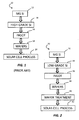
- FIGURE 1 is a prior art flow diagram depicting generally the known processes for forming a solar cell
- FIGURE 2 shows generally an overall solar cell formation process that may incorporate the teachings of the disclosed subject matter
- FIGURE 3 illustrates one embodiment of a process environment in which to achieve the results of the present disclosure
- FIGURE 4 shows a process flow according to the present disclosure for a higher purity silicon ingot from a low-grade silicon feedstock
- FIGUREs 5 and 6 present an embodiment a molten silicon removal process as disclosed by the present subject matter
- FIGUREs 7 and 8 illustrate various forms of molten silicon pre-conditioning as may be application to the present disclosure
- FIGUREs 9 through 11 present an alternative embodiment silicon removal process that is not part of the invention.
- FIGUREs 12 and 13 exhibit an alternative embodiment silicon removal process within the scope of the present disclosure.
- FIGUREs 14 and 15 provide different aspects of a crucible device that may find application within the subject matter of the present disclosure.
- the method and system of the present disclosure provide a semiconductor ingot formation process for producing a higher purity silicon or semiconductor ingot using a low purity or high impurity silicon or semiconductor feedstock.
- the presently disclosed process saves one melting process by combining previously separately performed processing steps, as well as making better use of the inherent cooling phase in the silicon ingot formation process.
- the present disclosure includes a pathway for removing molten silicon to leave the silicon ingot while the ingot formation takes place.
- the molten silicon that the disclosed subject matter removes generally possesses a larger amount of impurities than the silicon ingot being formed.
- the ultimate advantage is reduction of total cost since lower-grade feedstock can be used for directional solidification of a silicon ingot.
- Ingots made by the presently disclosed process and system are of higher quality as compared to ingots produced by known directional solidification techniques using lower purity feedstock.
- certain ones of particular note include the ability to reduce the amount of metallic and non-metallic impurities present in a semiconductor ingot such as may be useful in solar cell fabrication.
- Another specific advantage is avoidance of high-concentration regions of non-metals, mainly B, P and C, in top regions of ingots made from UMG-Si feedstock materials.
- FIGURE 1 depicts a known process 10 beginning at step 12 .
- MG or other low-grade silicon enters known wafer forming process flow 10 .
- Known process flow 10 extracts high-grade silicon from MG silicon at step 14 .
- High-grade silicon extraction step 14 is a high-cost processing sequence resulting in EG silicon. This is the type of silicon feedstock material used for making the ingot in step 16 .
- Known process flow 10 includes slicing the silicon ingot, generally using a wire-saw to derive a silicon wafer at step 18 . The resulting silicon wafers then enter solar cell formation process 20 .
- FIGURE 2 depicts, in general terms, novel aspects of a solar cell forming process flow 30 wherein the present disclosure exhibits particular advantages.
- Process flow 30 includes using MG silicon at steps 32 that is purified to some degree to become RMG or UMG silicon.
- the silicon quality reached is still a low-grade silicon 34 .
- silicon quality 36 relates to much lower cost as compared to silicon quality 14 .
- low-grade silicon at step 36 possesses a higher content of metallic and other impurities as compared to silicon quality 14 .
- silicon ingot formation may occur.
- Step 40 represents the formation of silicon wafers, i.e., slicing from the silicon ingot.
- the disclosed solar cell forming process flow 30 may introduce a wafer treatment step 40 , also called pre-process step, before starting the cell process.
- the solar cell forming process occurs at step 42 .
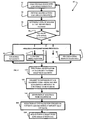
- FIGURE 3 illustrates process environment 50 .
- crucible 52 contains silicon melt 54 .
- Heating zones 58 surround the sides and bottom of crucible 42 .
- Isolation chamber 60 further establishes a process environment in conjunction with crucible 52 for temperature control and to establish a process atmosphere.
- Water cooling system 62 surrounds isolation chamber 60 , which camera 64 may penetrate to allow observation of silicon melt 52 .
- Process environment 50 has a height 66 , which crucible 54 spans vertically. However, for enhanced process control dropping mechanism 68 , which has a radius 70 may move vertically downward within lower frame 72 to expose different portions of crucible 54 to different temperature heating zones 58 more rapidly or at in more varying ways that can direct heating zone control.
- Processing environment 50 provides a sealed growth chamber having a vacuum of, for example, below 1x10 -3 Torr and cycle purged with argon to 10 psig several times to expel any oxygen remaining in the chamber.
- Heating zones 58 may be heated by a multi-turn induction coil in a parallel circuit with a tuning capacitor bank.
- FIGURE 4 presents an exemplary flowchart 80 for the presently disclosed silicon ingot formation process.
- silicon ingot forming process 80 loads a crucible, such as crucible 54 or the various crucible embodiments disclosed below, with low-grade silicon feedstock.
- molten silicon forms from the low-grade silicon feedstock by virtue of a heating process.
- a determination of whether the silicon melt forms below a predetermined pathway for its removal occurs at step 86 . If so, a next test 88 determines whether there is the need to add more low-grade silicon feedstock to the crucible.
- this determination is to assure that, as the directional solidification of the silicon melt 52 forms a higher grade silicon ingot, the progressively contaminated silicon melt ultimately has a path for its removal in the molten state.
- preconditioning silicon melt 52 may occur.
- Such preconditioning steps may include one or a combination of the steps for extracting impurities deriving from the low-grade silicon.
- the various silicon melt preconditioning steps may include a gas bubble nucleation step 90 , an ultrasonic energy agitation step 92 , or a combination of such steps or further steps including electromagnetic energy transfer to the melt , such as ellipsis 94 depicts. Moreover, as arrow 96 suggests, such steps may be bypassed. As step 98 further shows, such preconditioning may include a step of including various additives to silicon melt 52 .
- the process of the present disclosure includes initiation of directional solidification of silicon melt 52 to begin silicon ingot formation, at step 100 .
- a phase transformation of the silicon from liquid to solid occurs. Due to the phase transformation, expansion of the silicon volume within crucible 54 occurs, increasing the level of now combined molten and solidified silicon, as step 102 depicts.
- a separation of the molten silicon takes place. This separation occurs due to the physical characteristics of one or more embodiments of crucible 52 as shown and described in greater detail below.
- step 104 With the separation of molten silicon from crystallized silicon, as step 104 indicates, the silicon that remains in crucible 52 is of a higher purity than the silicon feedstock from which the silicon melt forms.
- the extraction of the silicon melt takes with it a higher concentration of impurities. The result is, in essence, the elimination or substantial reduction in the likelihood that impurities from the silicon melt 52 will back diffuse into the silicon ingot.
- step 106 may occur.
- ingot formation process 80 reduces crystallization stresses that arise within a silicon ingot during more rapid cooling processes.
- a lower concern for impurity back diffusion during a slower cooling process allows for controlling the rate of crystallized silicon cooling so as to relieve crystallization stresses.
- the reduced crystallization stress in the resulting silicon ingot yet further yields a higher purity silicon ingot, as step 108 shows.
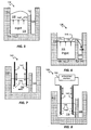
- FIGUREs 5 and 6 show in more detail aspects of step 102 of process flow 80 , wherein volumetric expansion of silicon in the solid or crystallizing form facilitates the removal of the increasingly contaminated silicon melt.
- process state 110 which includes a crucible 112 that provides a pathway for the silicon melt removal.
- Crucible 112 contains in process volume 114 both silicon ingot portion 116 and silicon melt 118 .
- Interface 120 separates silicon ingot portion 116 from silicon melt 118 .
- Crucible 112 further contains interstitial wall 122 separating process volume 114 from silicon melt flow volume 124 .
- FIGURE 6 shows the progressive raising of interface 120 at state 130 of silicon ingot formation process 80 .
- the effect is raise silicon melt at and above the lower height of interstitial wall 122. That is, the lower height of interstitial wall 122 forms a pathway 132 for the removal of silicon melt 118 .
- pathway 132 may be formed in numerous ways.
- the embodiment of FIGURES and 6 show one desirable, yet ingeniously simple way to cause the removal of silicon melt 118 from the ingot formation process volume 114 of crucible 112 .
- FIGUREs 7 and 8 show, respectively, the use of bubble nucleation and the combination of bubble nucleation and ultrasonic energy agitation for the purpose of facilitating the extraction of impurities during the early stages of directional silicon solidification.
- process state 140 wherein gas tubes 142 may be inserted into silicon melt 118 .
- Silicon melt 118 may receive through gas tubes certain amounts of gases such as oxygen, nitrogen, hydrogen, water vapor, CO 2 or Chlorine-containing gases such as HCl or combinations of the above gases and other gases. These gases react with impurities dissolved in the silicon melt 118 and form volatile compounds which evaporate from the melt. This can result in a more pure silicon ingot portion 116 ( FIGURE 5 ) during subsequent directional solidification step 100 of silicon ingot formation process 80 .
- FIGURE 8 shows in state 150 one embodiment of a silicon melt 118 preconditioning step 92 , wherein an ultrasonic energy source 152 may connect with gas tubes 142 . That is, gas tube 142 may not only serve as a conduit for delivery of nucleation bubbles 114 , but may also serve as an ultrasonic energy path for transmitting energy from ultrasonic energy source 152 into silicon melt 118 .
- the preconditioning of silicon melt 118 promotes a more pure resulting silicon melt portion 116 by extracting impurities deriving from the low-grade silicon.
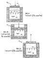
- FIGUREs 9 through 11 expand the concept of a pathway for the removal of the contaminated silicon melt. However, this part of the concept does not belong to the invention.
- FIGURE 9 shows that, in conjunction with a crucible, such as crucible 54 , there may be a silicon ingot portion 116 and a silicon melt 118 with interface 120 . Since, as has been explained, with the growth of silicon ingot portion 116 , impurities have concentrated in silicon melt 118 .
- the embodiment of FIGURE 9 demonstrates one path for removing the contaminated silicon melt 188 .
- FIGUREs 9 through 11 which are not part of the invention; show process stage 130 in which porous felt device 132 provides a material that demonstrates a significantly higher melting temperature than that of silicon melt 118 .
- porous felt device 132 provides a material that demonstrates a significantly higher melting temperature than that of silicon melt 118 .
- FIGURE 10 demonstrates in process stage 134 that porous felt device 132 has absorbed a significant portion, if not all of silicon melt 118 , thereby permitting the removal of contaminated silicon melt 118 from crucible 54 .
- FIGURE 11 shows in process stage 136 the removal of porous felt device 122 from crucible 54 , taking with it contaminated silicon melt 118 .
- FIGUREs 12 and 13 depict a further embodiment of the present disclosure wherein the pathway for removal of silicon melt 118 includes a movable flow valve device.
- FIGURE 12 depicts a process state 140 for a crucible 142 embodiment that includes a two-part flow valve assembly 144 .
- Flow-valve assembly 144 includes valve stem 146 , which penetrates through crucible outer aperture 148 and inner aperture 150 of interstitial wall 152 . When inserted through both outer aperture 148 and inner aperture 150 , valve stem 146 maintains an empty silicon melt 118 flow volume 154 .
- silicon melt 118 develops within crucible process volume 152 above both interface 120 and inner aperture 150 .
- valve stem 146 may be withdrawn through inner aperture 150 .
- FIGURE 13 shows in process state 160 that by withdrawing valve stem 146 from inner aperture 150 , while maintain valve stem 146 within outer aperture 148 a pathway for silicon melt 118 to flow into flow volume 154 .
- the flow of silicon melt 118 through the pathway of inner aperture 150 and into flow volume 154 removes from process volume 152 the contaminated silicon melt 118 , thereby preventing a significant degree of back diffusion of contaminants in a subsequent processing steps.
- FIGUREs 14 and 15 demonstrate yet a further embodiment of a crucible device 170 that is suitable for achieving the purposes of the present disclosure.
- crucible device 170 may include process volume 172 for receiving a low-grade silicon feedstock and producing there from silicon ingot portion.
- Inner wall 174 may surround process volume 172 .
- Flow volume 176 surrounds inner wall 174
- outer wall 178 surrounds flow volume 176 .
- FIGURE 15 further depicts crucible device 170 to include flow-valve assembly 144 having, as described above, valve stem 146 , which penetrates through flow volume outer aperture 180 of outer wall 178 and process environment 172 inner aperture 182 .
- Operation flow-valve assembly 144 is as described above, with the distinction that with flow volume 176 surrounding inner wall 174 , withdrawal of valve stem 146 causes silicon melt 118 to surround inner wall 174 .
- the disclosed subject matter provides a method and system for forming a silicon ingot which includes forming within a crucible device a molten silicon from a low-grade silicon feedstock and performing a directional solidification of the molten silicon to form a silicon ingot within the crucible device.
- the directional solidification forms a generally solidified quantity of silicon and a generally molten quantity of silicon.
- the method and system include removing from the crucible device at least a portion of the generally molten quantity of silicon while retaining within the crucible device the generally solidified quantity of silicon. Controlling the directional solidification of the generally solidified quantity of silicon forms a silicon ingot possessing a generally higher grade of silicon than the low-grade silicon feedstock.
- Such control may include extending the duration of the directional solidification of the generally solidified quantity of silicon for reducing material stresses arising from the crystallization of the silicon ingot.
- the method and system may pre-condition the molten silicon for extracting impurities deriving from the low-grade silicon, such as by introducing bubble nucleation into the molten silicon, transmitting ultrasonic energy or electromagnetic energy into the molten silicon and combining with the molten silicon an additive for aiding in the extraction of the impurities from the molten silicon.
- Various embodiments of the present disclosure include removing from the crucible device at least a portion of the generally molten quantity of silicon by flowing the generally molten quantity of silicon via a pathway associated with the crucible device.
- Embodiments of the pathway may include a lower interstitial wall separating a first volume of the crucible device from a second volume of the crucible device, the first volume of the crucible device containing the generally solidified quantity of silicon and the generally molten quantity of silicon.
- the lower interstitial wall further having a height approximating a height of a predetermined interface level between the generally solidified quantity of silicon and the generally molten quantity of silicon at a predetermined point during the directional solidification.
- the lower interstitial wall permits at least a portion of the generally molten quantity of silicon to flow from the first volume of the crucible device to the second volume of the crucible device, thereby separating the portion of the generally molten quantity of silicon from the generally solidified quantity of silicon.
- Another embodiment flows a portion of the generally molten quantity of silicon into the second volume surrounding the first volume.
- Another pathway may include a felt device for absorbing the generally molten quantity of silicon that may be submersed into the generally molten quantity of silicon. The molten silicon is absorbed into the felt device and removed to take with it the absorbed portion of the generally molten silicon.
- the pathway comprises a drain conduit and a plug device associated to control flow of the generally molten quantity of silicon through the drain conduit and further comprising the step of controllably positioning the plug device for controlling flow of the generally molten quantity of silicon from the crucible device.
- the method disassociates the generally molten quantity of silicon from the generally solidified quantity of silicon.
- Still another embodiment of the present disclosure provides a drain conduit separating a first volume of the crucible device from a second volume of the crucible device.
- a plug device associates to control flow of the generally molten quantity of silicon through the drain conduit. The process further controllably positions the plug device for controlling flow of molten silicon from the first volume to the second volume for disassociating the molten silicon from silicon.
- the second volume may surround the first volume.
- an improvement in the properties of low-grade semiconductor materials such as upgraded metallurgical-grade silicon (UMG) occurs.
- U1VIG silicon for example, in producing solar cells as may be used in solar power generation and related uses.
- the method and system of the present disclosure moreover, particularly benefits the formation of semiconductor solar cells using UMG or other non-electronic grade semiconductor materials.
- the present disclosure may allow the formation of solar cells in greater quantities and in a greater number of fabrication facilities than has heretofore been possible.
Landscapes
- Engineering & Computer Science (AREA)
- Manufacturing & Machinery (AREA)
- Physics & Mathematics (AREA)
- Condensed Matter Physics & Semiconductors (AREA)
- Electromagnetism (AREA)
- General Physics & Mathematics (AREA)
- Computer Hardware Design (AREA)
- Microelectronics & Electronic Packaging (AREA)
- Power Engineering (AREA)
- Silicon Compounds (AREA)
- Photovoltaic Devices (AREA)
Applications Claiming Priority (2)
| Application Number | Priority Date | Filing Date | Title |
|---|---|---|---|
| US11/828,734 US7955433B2 (en) | 2007-07-26 | 2007-07-26 | Method and system for forming a silicon ingot using a low-grade silicon feedstock |
| PCT/US2008/071234 WO2009015356A1 (en) | 2007-07-26 | 2008-07-25 | Method and system for forming a silicon ingot using a low-grade silicon feedstock |
Publications (3)
| Publication Number | Publication Date |
|---|---|
| EP2179078A1 EP2179078A1 (en) | 2010-04-28 |
| EP2179078A4 EP2179078A4 (en) | 2010-08-04 |
| EP2179078B1 true EP2179078B1 (en) | 2012-03-07 |
Family
ID=40281853
Family Applications (1)
| Application Number | Title | Priority Date | Filing Date |
|---|---|---|---|
| EP08796655A Not-in-force EP2179078B1 (en) | 2007-07-26 | 2008-07-25 | Method and system for forming a silicon ingot using a low-grade silicon feedstock |
Country Status (7)
| Country | Link |
|---|---|
| US (2) | US7955433B2 (zh) |
| EP (1) | EP2179078B1 (zh) |
| JP (1) | JP5462988B2 (zh) |
| CN (1) | CN102037163B (zh) |
| AT (1) | ATE548487T1 (zh) |
| ES (1) | ES2383928T3 (zh) |
| WO (1) | WO2009015356A1 (zh) |
Cited By (1)
| Publication number | Priority date | Publication date | Assignee | Title |
|---|---|---|---|---|
| US8882912B2 (en) | 2007-07-26 | 2014-11-11 | Silicor Materials Inc. | Method and system for forming a silicon ingot using a low-grade silicon feedstock |
Families Citing this family (14)
| Publication number | Priority date | Publication date | Assignee | Title |
|---|---|---|---|---|
| KR101318427B1 (ko) * | 2008-08-15 | 2013-10-16 | 가부시키가이샤 아루박 | 실리콘의 정제 방법 |
| US8679888B2 (en) * | 2008-09-24 | 2014-03-25 | The Board Of Trustees Of The University Of Illinois | Arrays of ultrathin silicon solar microcells |
| US20100213643A1 (en) * | 2009-02-26 | 2010-08-26 | Gadgil Prasad N | Rapid synthesis of polycrystalline silicon sheets for photo-voltaic solar cell manufacturing |
| TWI379430B (en) * | 2009-04-16 | 2012-12-11 | Atomic Energy Council | A method of fabricating a thin interface for internal light reflection and impurities isolation |
| CN101575733B (zh) * | 2009-05-22 | 2011-07-27 | 北京航空航天大学 | 一种工业化生产太阳能级多晶硅的方法 |
| CN101775650B (zh) * | 2010-03-12 | 2013-01-30 | 厦门大学 | 一种太阳能多晶硅铸锭的制备方法 |
| CN102021650B (zh) * | 2010-12-31 | 2012-06-06 | 常州天合光能有限公司 | 一种大型多晶锭的生产方法 |
| KR20140017604A (ko) | 2011-03-15 | 2014-02-11 | 지티에이티 코포레이션 | 결정성장 장치용 자동 비전 시스템 |
| JP5512647B2 (ja) * | 2011-12-22 | 2014-06-04 | シャープ株式会社 | シリコンの精製方法、吸収ユニット、およびシリコン精製装置 |
| CN103266351B (zh) * | 2013-05-31 | 2015-08-12 | 大连理工大学 | 多晶硅铸锭硅固液分离方法及设备 |
| US10402360B2 (en) * | 2016-06-10 | 2019-09-03 | Johnson Controls Technology Company | Building management system with automatic equipment discovery and equipment model distribution |
| JP6919633B2 (ja) * | 2018-08-29 | 2021-08-18 | 信越半導体株式会社 | 単結晶育成方法 |
| JP7052645B2 (ja) * | 2018-08-29 | 2022-04-12 | 信越半導体株式会社 | 単結晶育成方法 |
| AU2019444019B2 (en) * | 2019-04-30 | 2022-03-10 | Wacker Chemie Ag | Method for refining crude silicon melts using a particulate mediator |
Family Cites Families (30)
| Publication number | Priority date | Publication date | Assignee | Title |
|---|---|---|---|---|
| US3012865A (en) * | 1957-11-25 | 1961-12-12 | Du Pont | Silicon purification process |
| DE2143112A1 (de) * | 1971-08-27 | 1973-03-01 | Siemens Ag | Verfahren zur erzielung eines gleichmaessigen radialen widerstandsverlaufs beim herstellen eines halbleiter-einkristallstabes durch tiegelfreies zonenschmelzen |
| SU661966A1 (ru) * | 1976-11-23 | 1980-04-05 | Всесоюзный Научно-Исследовательский Институт Монокристаллов И Особо Чистых Химических Веществ "Вниимонокристалл" | Устройство дл выт гивани монокристаллов из расплава |
| FR2430917A1 (fr) * | 1978-07-11 | 1980-02-08 | Comp Generale Electricite | Procede et dispositif d'elaboration de silicium polycristallin |
| JPS5933554B2 (ja) * | 1982-08-19 | 1984-08-16 | 株式会社東芝 | 結晶成長装置 |
| US4565671A (en) * | 1983-08-05 | 1986-01-21 | Kabushiki Kaisha Toshiba | Single crystal manufacturing apparatus |
| DE3411955A1 (de) | 1984-03-30 | 1985-10-10 | Siemens AG, 1000 Berlin und 8000 München | Verfahren und vorrichtung zum abtrennen fester bestandteile aus fluessigem silicium |
| EP0221051A1 (en) * | 1985-04-16 | 1987-05-13 | Energy Materials Corporation | Method and apparatus for growing single crystal bodies |
| JPS62291977A (ja) * | 1986-06-06 | 1987-12-18 | シ−メンス、アクチエンゲゼルシヤフト | 太陽電池用シリコン盤の切り出し方法と装置 |
| US5314667A (en) * | 1991-03-04 | 1994-05-24 | Lim John C | Method and apparatus for single crystal silicon production |
| US5580171A (en) * | 1995-07-24 | 1996-12-03 | Lim; John C. | Solids mixing, storing and conveying system for use with a furnace for single crystal silicon production |
| EP0796820B1 (en) * | 1996-03-19 | 2000-07-19 | Kawasaki Steel Corporation | Process and apparatus for refining silicon |
| JP3325900B2 (ja) * | 1996-10-14 | 2002-09-17 | 川崎製鉄株式会社 | 多結晶シリコンの製造方法及び装置、並びに太陽電池用シリコン基板の製造方法 |
| CA2232777C (en) | 1997-03-24 | 2001-05-15 | Hiroyuki Baba | Method for producing silicon for use in solar cells |
| JP3520957B2 (ja) * | 1997-06-23 | 2004-04-19 | シャープ株式会社 | 多結晶半導体インゴットの製造方法および装置 |
| JP3741043B2 (ja) * | 2000-03-03 | 2006-02-01 | 信越半導体株式会社 | 単結晶引上げ装置の湯漏れ受皿 |
| FR2808809B1 (fr) | 2000-05-11 | 2003-06-27 | Emix | Installation de fabrication en continu de barreau de silicium multicristallin |
| JP3698080B2 (ja) * | 2001-09-11 | 2005-09-21 | 三菱住友シリコン株式会社 | 単結晶引上げ方法 |
| US20050139148A1 (en) * | 2002-02-04 | 2005-06-30 | Hiroyasu Fujiwara | Silicon purifying method, slag for purifying silicon and purified silicon |
| AU2003277041A1 (en) * | 2002-09-27 | 2004-04-19 | Astropower, Inc. | Methods and systems for purifying elements |
| JP2004161575A (ja) * | 2002-11-15 | 2004-06-10 | Sumitomo Titanium Corp | 多結晶シリコンインゴット及び部材の製造方法 |
| US20050066881A1 (en) * | 2003-09-25 | 2005-03-31 | Canon Kabushiki Kaisha | Continuous production method for crystalline silicon and production apparatus for the same |
| US7635414B2 (en) * | 2003-11-03 | 2009-12-22 | Solaicx, Inc. | System for continuous growing of monocrystalline silicon |
| JP4947455B2 (ja) * | 2005-08-16 | 2012-06-06 | 則近 山内 | 電子ビームを用いたシリコンの精錬方法及び装置 |
| JP4817761B2 (ja) * | 2005-08-30 | 2011-11-16 | 京セラ株式会社 | 半導体インゴット及び太陽電池素子の製造方法 |
| US8262797B1 (en) * | 2007-03-13 | 2012-09-11 | Solaicx, Inc. | Weir design providing optimal purge gas flow, melt control, and temperature stabilization for improved single crystal growth in a continuous Czochralski process |
| US7955433B2 (en) | 2007-07-26 | 2011-06-07 | Calisolar, Inc. | Method and system for forming a silicon ingot using a low-grade silicon feedstock |
| US8475591B2 (en) * | 2008-08-15 | 2013-07-02 | Varian Semiconductor Equipment Associates, Inc. | Method of controlling a thickness of a sheet formed from a melt |
| US7998224B2 (en) * | 2008-10-21 | 2011-08-16 | Varian Semiconductor Equipment Associates, Inc. | Removal of a sheet from a production apparatus |
| US8652257B2 (en) * | 2010-02-22 | 2014-02-18 | Lev George Eidelman | Controlled gravity feeding czochralski apparatus with on the way melting raw material |
-
2007
- 2007-07-26 US US11/828,734 patent/US7955433B2/en not_active Expired - Fee Related
-
2008
- 2008-07-25 EP EP08796655A patent/EP2179078B1/en not_active Not-in-force
- 2008-07-25 ES ES08796655T patent/ES2383928T3/es active Active
- 2008-07-25 WO PCT/US2008/071234 patent/WO2009015356A1/en active Application Filing
- 2008-07-25 JP JP2010518420A patent/JP5462988B2/ja not_active Expired - Fee Related
- 2008-07-25 AT AT08796655T patent/ATE548487T1/de active
- 2008-07-25 CN CN2008801096076A patent/CN102037163B/zh not_active Expired - Fee Related
-
2011
- 2011-02-25 US US13/034,956 patent/US8882912B2/en not_active Expired - Fee Related
Cited By (1)
| Publication number | Priority date | Publication date | Assignee | Title |
|---|---|---|---|---|
| US8882912B2 (en) | 2007-07-26 | 2014-11-11 | Silicor Materials Inc. | Method and system for forming a silicon ingot using a low-grade silicon feedstock |
Also Published As
| Publication number | Publication date |
|---|---|
| EP2179078A4 (en) | 2010-08-04 |
| CN102037163B (zh) | 2013-01-30 |
| ES2383928T3 (es) | 2012-06-27 |
| CN102037163A (zh) | 2011-04-27 |
| ATE548487T1 (de) | 2012-03-15 |
| JP5462988B2 (ja) | 2014-04-02 |
| US20110211995A1 (en) | 2011-09-01 |
| EP2179078A1 (en) | 2010-04-28 |
| US7955433B2 (en) | 2011-06-07 |
| JP2010534614A (ja) | 2010-11-11 |
| WO2009015356A1 (en) | 2009-01-29 |
| US8882912B2 (en) | 2014-11-11 |
| US20090028773A1 (en) | 2009-01-29 |
Similar Documents
| Publication | Publication Date | Title |
|---|---|---|
| EP2179078B1 (en) | Method and system for forming a silicon ingot using a low-grade silicon feedstock | |
| KR100939299B1 (ko) | 실리콘 웨이퍼 및 그 제조 방법 | |
| KR100945517B1 (ko) | 다결정 실리콘 잉곳의 제조방법 | |
| US7811356B2 (en) | Method of purifying metal | |
| US20080178793A1 (en) | Method and system for forming a higher purity semiconductor ingot using low purity semiconductor feedstock | |
| US20090314198A1 (en) | Device and method for production of semiconductor grade silicon | |
| US8790584B2 (en) | System for refining UMG Si using steam plasma torch | |
| CN101591807A (zh) | 掺氮的定向凝固铸造单晶硅及其制备方法 | |
| US20100178195A1 (en) | Method of solidifying metallic silicon | |
| TWI442478B (zh) | 矽基板及其製造方法 | |
| US20090098715A1 (en) | Process for manufacturing silicon wafers for solar cell | |
| CN102312291A (zh) | 一种掺杂的铸造单晶硅及制备方法 | |
| CN104649274A (zh) | 电子束连续熔炼去除多晶硅中氧杂质的方法及其装置 | |
| CN114250503A (zh) | 一种零位错p型锗单晶制备方法 | |
| Kalejs | Silicon ribbons for solar cells | |
| JP5401809B2 (ja) | シリコン基板とその製造方法 | |
| JP5401808B2 (ja) | シリコン基板とその製造方法 | |
| CN108796606B (zh) | 太阳能级多晶硅制备装置 | |
| CN203699921U (zh) | 电子束连续熔炼去除多晶硅中氧杂质的装置 | |
| CN112342616B (zh) | 一种晶体硅棒的加工方法及其产品 | |
| JP2010095421A (ja) | 多結晶シリコンの製造方法及び多結晶シリコンウェーハ | |
| Schmid et al. | Directional Solidification of Mg Silicon by Heat Exchanger Method (HEM) for Photovoltaic Applications | |
| JP5220935B1 (ja) | 太陽電池用シリコン、多結晶シリコン材料、多結晶シリコン太陽電池および太陽電池用シリコンの製造方法 | |
| Cohen et al. | Floating crystalline Si-foils for photovoltaic applications |
Legal Events
| Date | Code | Title | Description |
|---|---|---|---|
| PUAI | Public reference made under article 153(3) epc to a published international application that has entered the european phase |
Free format text: ORIGINAL CODE: 0009012 |
|
| 17P | Request for examination filed |
Effective date: 20100226 |
|
| AK | Designated contracting states |
Kind code of ref document: A1 Designated state(s): AT BE BG CH CY CZ DE DK EE ES FI FR GB GR HR HU IE IS IT LI LT LU LV MC MT NL NO PL PT RO SE SI SK TR |
|
| AX | Request for extension of the european patent |
Extension state: AL BA MK RS |
|
| A4 | Supplementary search report drawn up and despatched |
Effective date: 20100706 |
|
| RIC1 | Information provided on ipc code assigned before grant |
Ipc: C30B 11/00 20060101ALI20100630BHEP Ipc: C30B 29/06 20060101AFI20100630BHEP |
|
| DAX | Request for extension of the european patent (deleted) | ||
| REG | Reference to a national code |
Ref country code: HK Ref legal event code: DE Ref document number: 1143409 Country of ref document: HK |
|
| 17Q | First examination report despatched |
Effective date: 20110301 |
|
| REG | Reference to a national code |
Ref country code: DE Ref legal event code: R079 Ref document number: 602008013996 Country of ref document: DE Free format text: PREVIOUS MAIN CLASS: C30B0009040000 Ipc: C30B0029060000 |
|
| RIC1 | Information provided on ipc code assigned before grant |
Ipc: C30B 11/00 20060101ALI20110811BHEP Ipc: C30B 29/06 20060101AFI20110811BHEP |
|
| GRAP | Despatch of communication of intention to grant a patent |
Free format text: ORIGINAL CODE: EPIDOSNIGR1 |
|
| GRAS | Grant fee paid |
Free format text: ORIGINAL CODE: EPIDOSNIGR3 |
|
| GRAA | (expected) grant |
Free format text: ORIGINAL CODE: 0009210 |
|
| AK | Designated contracting states |
Kind code of ref document: B1 Designated state(s): AT BE BG CH CY CZ DE DK EE ES FI FR GB GR HR HU IE IS IT LI LT LU LV MC MT NL NO PL PT RO SE SI SK TR |
|
| RAP1 | Party data changed (applicant data changed or rights of an application transferred) |
Owner name: CALISOLAR, INC. |
|
| REG | Reference to a national code |
Ref country code: GB Ref legal event code: FG4D |
|
| REG | Reference to a national code |
Ref country code: AT Ref legal event code: REF Ref document number: 548487 Country of ref document: AT Kind code of ref document: T Effective date: 20120315 Ref country code: CH Ref legal event code: EP |
|
| REG | Reference to a national code |
Ref country code: IE Ref legal event code: FG4D |
|
| REG | Reference to a national code |
Ref country code: DE Ref legal event code: R096 Ref document number: 602008013996 Country of ref document: DE Effective date: 20120503 |
|
| REG | Reference to a national code |
Ref country code: ES Ref legal event code: FG2A Ref document number: 2383928 Country of ref document: ES Kind code of ref document: T3 Effective date: 20120627 |
|
| REG | Reference to a national code |
Ref country code: NL Ref legal event code: VDEP Effective date: 20120307 |
|
| PG25 | Lapsed in a contracting state [announced via postgrant information from national office to epo] |
Ref country code: LT Free format text: LAPSE BECAUSE OF FAILURE TO SUBMIT A TRANSLATION OF THE DESCRIPTION OR TO PAY THE FEE WITHIN THE PRESCRIBED TIME-LIMIT Effective date: 20120307 Ref country code: NL Free format text: LAPSE BECAUSE OF FAILURE TO SUBMIT A TRANSLATION OF THE DESCRIPTION OR TO PAY THE FEE WITHIN THE PRESCRIBED TIME-LIMIT Effective date: 20120307 Ref country code: HR Free format text: LAPSE BECAUSE OF FAILURE TO SUBMIT A TRANSLATION OF THE DESCRIPTION OR TO PAY THE FEE WITHIN THE PRESCRIBED TIME-LIMIT Effective date: 20120307 Ref country code: NO Free format text: LAPSE BECAUSE OF FAILURE TO SUBMIT A TRANSLATION OF THE DESCRIPTION OR TO PAY THE FEE WITHIN THE PRESCRIBED TIME-LIMIT Effective date: 20120607 |
|
| LTIE | Lt: invalidation of european patent or patent extension |
Effective date: 20120307 |
|
| PG25 | Lapsed in a contracting state [announced via postgrant information from national office to epo] |
Ref country code: LV Free format text: LAPSE BECAUSE OF FAILURE TO SUBMIT A TRANSLATION OF THE DESCRIPTION OR TO PAY THE FEE WITHIN THE PRESCRIBED TIME-LIMIT Effective date: 20120307 Ref country code: GR Free format text: LAPSE BECAUSE OF FAILURE TO SUBMIT A TRANSLATION OF THE DESCRIPTION OR TO PAY THE FEE WITHIN THE PRESCRIBED TIME-LIMIT Effective date: 20120608 Ref country code: FI Free format text: LAPSE BECAUSE OF FAILURE TO SUBMIT A TRANSLATION OF THE DESCRIPTION OR TO PAY THE FEE WITHIN THE PRESCRIBED TIME-LIMIT Effective date: 20120307 |
|
| REG | Reference to a national code |
Ref country code: AT Ref legal event code: MK05 Ref document number: 548487 Country of ref document: AT Kind code of ref document: T Effective date: 20120307 |
|
| PG25 | Lapsed in a contracting state [announced via postgrant information from national office to epo] |
Ref country code: CY Free format text: LAPSE BECAUSE OF FAILURE TO SUBMIT A TRANSLATION OF THE DESCRIPTION OR TO PAY THE FEE WITHIN THE PRESCRIBED TIME-LIMIT Effective date: 20120307 |
|
| PG25 | Lapsed in a contracting state [announced via postgrant information from national office to epo] |
Ref country code: BE Free format text: LAPSE BECAUSE OF FAILURE TO SUBMIT A TRANSLATION OF THE DESCRIPTION OR TO PAY THE FEE WITHIN THE PRESCRIBED TIME-LIMIT Effective date: 20120307 Ref country code: IS Free format text: LAPSE BECAUSE OF FAILURE TO SUBMIT A TRANSLATION OF THE DESCRIPTION OR TO PAY THE FEE WITHIN THE PRESCRIBED TIME-LIMIT Effective date: 20120707 Ref country code: RO Free format text: LAPSE BECAUSE OF FAILURE TO SUBMIT A TRANSLATION OF THE DESCRIPTION OR TO PAY THE FEE WITHIN THE PRESCRIBED TIME-LIMIT Effective date: 20120307 Ref country code: PL Free format text: LAPSE BECAUSE OF FAILURE TO SUBMIT A TRANSLATION OF THE DESCRIPTION OR TO PAY THE FEE WITHIN THE PRESCRIBED TIME-LIMIT Effective date: 20120307 Ref country code: SI Free format text: LAPSE BECAUSE OF FAILURE TO SUBMIT A TRANSLATION OF THE DESCRIPTION OR TO PAY THE FEE WITHIN THE PRESCRIBED TIME-LIMIT Effective date: 20120307 Ref country code: EE Free format text: LAPSE BECAUSE OF FAILURE TO SUBMIT A TRANSLATION OF THE DESCRIPTION OR TO PAY THE FEE WITHIN THE PRESCRIBED TIME-LIMIT Effective date: 20120307 Ref country code: CZ Free format text: LAPSE BECAUSE OF FAILURE TO SUBMIT A TRANSLATION OF THE DESCRIPTION OR TO PAY THE FEE WITHIN THE PRESCRIBED TIME-LIMIT Effective date: 20120307 Ref country code: SE Free format text: LAPSE BECAUSE OF FAILURE TO SUBMIT A TRANSLATION OF THE DESCRIPTION OR TO PAY THE FEE WITHIN THE PRESCRIBED TIME-LIMIT Effective date: 20120307 |
|
| PG25 | Lapsed in a contracting state [announced via postgrant information from national office to epo] |
Ref country code: PT Free format text: LAPSE BECAUSE OF FAILURE TO SUBMIT A TRANSLATION OF THE DESCRIPTION OR TO PAY THE FEE WITHIN THE PRESCRIBED TIME-LIMIT Effective date: 20120709 Ref country code: SK Free format text: LAPSE BECAUSE OF FAILURE TO SUBMIT A TRANSLATION OF THE DESCRIPTION OR TO PAY THE FEE WITHIN THE PRESCRIBED TIME-LIMIT Effective date: 20120307 |
|
| RAP2 | Party data changed (patent owner data changed or rights of a patent transferred) |
Owner name: SILICOR MATERIALS INC. |
|
| PLBE | No opposition filed within time limit |
Free format text: ORIGINAL CODE: 0009261 |
|
| STAA | Information on the status of an ep patent application or granted ep patent |
Free format text: STATUS: NO OPPOSITION FILED WITHIN TIME LIMIT |
|
| PG25 | Lapsed in a contracting state [announced via postgrant information from national office to epo] |
Ref country code: DK Free format text: LAPSE BECAUSE OF FAILURE TO SUBMIT A TRANSLATION OF THE DESCRIPTION OR TO PAY THE FEE WITHIN THE PRESCRIBED TIME-LIMIT Effective date: 20120307 Ref country code: AT Free format text: LAPSE BECAUSE OF FAILURE TO SUBMIT A TRANSLATION OF THE DESCRIPTION OR TO PAY THE FEE WITHIN THE PRESCRIBED TIME-LIMIT Effective date: 20120307 |
|
| 26N | No opposition filed |
Effective date: 20121210 |
|
| REG | Reference to a national code |
Ref country code: DE Ref legal event code: R082 Ref document number: 602008013996 Country of ref document: DE Representative=s name: DR. VOLKER VOSSIUS PATENT- UND RECHTSANWALTSKA, DE |
|
| PG25 | Lapsed in a contracting state [announced via postgrant information from national office to epo] |
Ref country code: MC Free format text: LAPSE BECAUSE OF NON-PAYMENT OF DUE FEES Effective date: 20120731 |
|
| REG | Reference to a national code |
Ref country code: CH Ref legal event code: PL |
|
| REG | Reference to a national code |
Ref country code: DE Ref legal event code: R082 Ref document number: 602008013996 Country of ref document: DE Representative=s name: DR. VOLKER VOSSIUS PATENT- UND RECHTSANWALTSKA, DE |
|
| REG | Reference to a national code |
Ref country code: DE Ref legal event code: R097 Ref document number: 602008013996 Country of ref document: DE Effective date: 20121210 |
|
| PG25 | Lapsed in a contracting state [announced via postgrant information from national office to epo] |
Ref country code: LI Free format text: LAPSE BECAUSE OF NON-PAYMENT OF DUE FEES Effective date: 20120731 Ref country code: CH Free format text: LAPSE BECAUSE OF NON-PAYMENT OF DUE FEES Effective date: 20120731 |
|
| REG | Reference to a national code |
Ref country code: DE Ref legal event code: R082 Ref document number: 602008013996 Country of ref document: DE Representative=s name: LKGLOBAL | LORENZ & KOPF PARTG MBB PATENTANWAE, DE Effective date: 20130227 Ref country code: DE Ref legal event code: R082 Ref document number: 602008013996 Country of ref document: DE Representative=s name: LKGLOBAL | LORENZ & KOPF PARTG MBB PATENTANWAE, DE Effective date: 20130311 Ref country code: DE Ref legal event code: R081 Ref document number: 602008013996 Country of ref document: DE Owner name: SILICOR MATERIALS INC., US Free format text: FORMER OWNER: CALISOLAR, INC., SUNNYVALE, US Effective date: 20130311 Ref country code: DE Ref legal event code: R082 Ref document number: 602008013996 Country of ref document: DE Representative=s name: DR. VOLKER VOSSIUS PATENT- UND RECHTSANWALTSKA, DE Effective date: 20130227 Ref country code: DE Ref legal event code: R082 Ref document number: 602008013996 Country of ref document: DE Representative=s name: DR. VOLKER VOSSIUS PATENT- UND RECHTSANWALTSKA, DE Effective date: 20130311 Ref country code: DE Ref legal event code: R082 Ref document number: 602008013996 Country of ref document: DE Representative=s name: SPIES DANNER & PARTNER PATENTANWAELTE PARTNERS, DE Effective date: 20130227 Ref country code: DE Ref legal event code: R082 Ref document number: 602008013996 Country of ref document: DE Representative=s name: SPIES DANNER & PARTNER PATENTANWAELTE PARTNERS, DE Effective date: 20130311 Ref country code: DE Ref legal event code: R081 Ref document number: 602008013996 Country of ref document: DE Owner name: SILICOR MATERIALS INC., PALO ALTO, US Free format text: FORMER OWNER: CALISOLAR, INC., SUNNYVALE, CALIF., US Effective date: 20130311 Ref country code: DE Ref legal event code: R082 Ref document number: 602008013996 Country of ref document: DE Representative=s name: LIFETECH IP SPIES DANNER & PARTNER PATENTANWAE, DE Effective date: 20130311 Ref country code: DE Ref legal event code: R082 Ref document number: 602008013996 Country of ref document: DE Representative=s name: LIFETECH IP SPIES DANNER & PARTNER PATENTANWAE, DE Effective date: 20130227 Ref country code: DE Ref legal event code: R082 Ref document number: 602008013996 Country of ref document: DE Representative=s name: KOPF WESTENBERGER WACHENHAUSEN PATENTANWAELTE , DE Effective date: 20130227 Ref country code: DE Ref legal event code: R082 Ref document number: 602008013996 Country of ref document: DE Representative=s name: KOPF WESTENBERGER WACHENHAUSEN PATENTANWAELTE , DE Effective date: 20130311 |
|
| REG | Reference to a national code |
Ref country code: IE Ref legal event code: MM4A |
|
| REG | Reference to a national code |
Ref country code: FR Ref legal event code: CA Effective date: 20130503 Ref country code: FR Ref legal event code: CD Owner name: SILICOR MATERIALS INC., US Effective date: 20130503 |
|
| PG25 | Lapsed in a contracting state [announced via postgrant information from national office to epo] |
Ref country code: IE Free format text: LAPSE BECAUSE OF NON-PAYMENT OF DUE FEES Effective date: 20120725 Ref country code: MT Free format text: LAPSE BECAUSE OF FAILURE TO SUBMIT A TRANSLATION OF THE DESCRIPTION OR TO PAY THE FEE WITHIN THE PRESCRIBED TIME-LIMIT Effective date: 20120307 Ref country code: BG Free format text: LAPSE BECAUSE OF FAILURE TO SUBMIT A TRANSLATION OF THE DESCRIPTION OR TO PAY THE FEE WITHIN THE PRESCRIBED TIME-LIMIT Effective date: 20120607 |
|
| REG | Reference to a national code |
Ref country code: DE Ref legal event code: R082 Ref document number: 602008013996 Country of ref document: DE Representative=s name: LKGLOBAL | LORENZ & KOPF PARTG MBB PATENTANWAE, DE Ref country code: DE Ref legal event code: R082 Ref document number: 602008013996 Country of ref document: DE Representative=s name: SPIES DANNER & PARTNER PATENTANWAELTE PARTNERS, DE Ref country code: DE Ref legal event code: R082 Ref document number: 602008013996 Country of ref document: DE Representative=s name: LIFETECH IP SPIES DANNER & PARTNER PATENTANWAE, DE Ref country code: DE Ref legal event code: R082 Ref document number: 602008013996 Country of ref document: DE Representative=s name: KOPF WESTENBERGER WACHENHAUSEN PATENTANWAELTE , DE |
|
| PG25 | Lapsed in a contracting state [announced via postgrant information from national office to epo] |
Ref country code: TR Free format text: LAPSE BECAUSE OF FAILURE TO SUBMIT A TRANSLATION OF THE DESCRIPTION OR TO PAY THE FEE WITHIN THE PRESCRIBED TIME-LIMIT Effective date: 20120307 |
|
| PG25 | Lapsed in a contracting state [announced via postgrant information from national office to epo] |
Ref country code: LU Free format text: LAPSE BECAUSE OF NON-PAYMENT OF DUE FEES Effective date: 20120725 |
|
| PG25 | Lapsed in a contracting state [announced via postgrant information from national office to epo] |
Ref country code: HU Free format text: LAPSE BECAUSE OF FAILURE TO SUBMIT A TRANSLATION OF THE DESCRIPTION OR TO PAY THE FEE WITHIN THE PRESCRIBED TIME-LIMIT Effective date: 20080725 |
|
| REG | Reference to a national code |
Ref country code: DE Ref legal event code: R082 Ref document number: 602008013996 Country of ref document: DE Representative=s name: LKGLOBAL | LORENZ & KOPF PARTG MBB PATENTANWAE, DE Ref country code: DE Ref legal event code: R082 Ref document number: 602008013996 Country of ref document: DE Representative=s name: KOPF WESTENBERGER WACHENHAUSEN PATENTANWAELTE , DE Ref country code: DE Ref legal event code: R082 Ref document number: 602008013996 Country of ref document: DE Representative=s name: LIFETECH IP SPIES DANNER & PARTNER PATENTANWAE, DE |
|
| REG | Reference to a national code |
Ref country code: FR Ref legal event code: PLFP Year of fee payment: 8 |
|
| PGFP | Annual fee paid to national office [announced via postgrant information from national office to epo] |
Ref country code: ES Payment date: 20150727 Year of fee payment: 8 Ref country code: GB Payment date: 20150727 Year of fee payment: 8 Ref country code: DE Payment date: 20150729 Year of fee payment: 8 |
|
| PGFP | Annual fee paid to national office [announced via postgrant information from national office to epo] |
Ref country code: FR Payment date: 20150717 Year of fee payment: 8 |
|
| PGFP | Annual fee paid to national office [announced via postgrant information from national office to epo] |
Ref country code: IT Payment date: 20150727 Year of fee payment: 8 |
|
| REG | Reference to a national code |
Ref country code: DE Ref legal event code: R082 Ref document number: 602008013996 Country of ref document: DE Representative=s name: LKGLOBAL | LORENZ & KOPF PARTG MBB PATENTANWAE, DE Ref country code: DE Ref legal event code: R082 Ref document number: 602008013996 Country of ref document: DE Representative=s name: KOPF WESTENBERGER WACHENHAUSEN PATENTANWAELTE , DE |
|
| REG | Reference to a national code |
Ref country code: DE Ref legal event code: R119 Ref document number: 602008013996 Country of ref document: DE |
|
| REG | Reference to a national code |
Ref country code: HK Ref legal event code: WD Ref document number: 1143409 Country of ref document: HK |
|
| GBPC | Gb: european patent ceased through non-payment of renewal fee |
Effective date: 20160725 |
|
| PG25 | Lapsed in a contracting state [announced via postgrant information from national office to epo] |
Ref country code: FR Free format text: LAPSE BECAUSE OF NON-PAYMENT OF DUE FEES Effective date: 20160801 Ref country code: DE Free format text: LAPSE BECAUSE OF NON-PAYMENT OF DUE FEES Effective date: 20170201 |
|
| REG | Reference to a national code |
Ref country code: FR Ref legal event code: ST Effective date: 20170331 |
|
| PG25 | Lapsed in a contracting state [announced via postgrant information from national office to epo] |
Ref country code: GB Free format text: LAPSE BECAUSE OF NON-PAYMENT OF DUE FEES Effective date: 20160725 |
|
| PG25 | Lapsed in a contracting state [announced via postgrant information from national office to epo] |
Ref country code: IT Free format text: LAPSE BECAUSE OF NON-PAYMENT OF DUE FEES Effective date: 20160725 |
|
| PG25 | Lapsed in a contracting state [announced via postgrant information from national office to epo] |
Ref country code: ES Free format text: LAPSE BECAUSE OF NON-PAYMENT OF DUE FEES Effective date: 20160726 |
|
| REG | Reference to a national code |
Ref country code: ES Ref legal event code: FD2A Effective date: 20181130 |