EP2151852B1 - Relâchement et transfert de couches tendues - Google Patents
Relâchement et transfert de couches tendues Download PDFInfo
- Publication number
- EP2151852B1 EP2151852B1 EP08290759.3A EP08290759A EP2151852B1 EP 2151852 B1 EP2151852 B1 EP 2151852B1 EP 08290759 A EP08290759 A EP 08290759A EP 2151852 B1 EP2151852 B1 EP 2151852B1
- Authority
- EP
- European Patent Office
- Prior art keywords
- layer
- substrate
- strained material
- islands
- strained
- Prior art date
- Legal status (The legal status is an assumption and is not a legal conclusion. Google has not performed a legal analysis and makes no representation as to the accuracy of the status listed.)
- Active
Links
- 239000000463 material Substances 0.000 claims description 145
- 239000000758 substrate Substances 0.000 claims description 134
- 238000000034 method Methods 0.000 claims description 28
- 239000005380 borophosphosilicate glass Substances 0.000 claims description 22
- 238000010438 heat treatment Methods 0.000 claims description 19
- 239000004065 semiconductor Substances 0.000 claims description 17
- 238000000059 patterning Methods 0.000 claims description 16
- 238000004519 manufacturing process Methods 0.000 claims description 15
- VYPSYNLAJGMNEJ-UHFFFAOYSA-N Silicium dioxide Chemical compound O=[Si]=O VYPSYNLAJGMNEJ-UHFFFAOYSA-N 0.000 claims description 14
- 230000015572 biosynthetic process Effects 0.000 claims description 13
- 229910052796 boron Inorganic materials 0.000 claims description 10
- 229910052594 sapphire Inorganic materials 0.000 claims description 10
- 239000010980 sapphire Substances 0.000 claims description 10
- 238000000151 deposition Methods 0.000 claims description 8
- 229910052681 coesite Inorganic materials 0.000 claims description 7
- 229910052906 cristobalite Inorganic materials 0.000 claims description 7
- 230000002040 relaxant effect Effects 0.000 claims description 7
- 229910052710 silicon Inorganic materials 0.000 claims description 7
- 239000000377 silicon dioxide Substances 0.000 claims description 7
- 229910052682 stishovite Inorganic materials 0.000 claims description 7
- 229910052905 tridymite Inorganic materials 0.000 claims description 7
- 239000010703 silicon Substances 0.000 claims description 6
- ZOXJGFHDIHLPTG-UHFFFAOYSA-N Boron Chemical compound [B] ZOXJGFHDIHLPTG-UHFFFAOYSA-N 0.000 claims description 5
- 238000010521 absorption reaction Methods 0.000 claims description 4
- BHEPBYXIRTUNPN-UHFFFAOYSA-N hydridophosphorus(.) (triplet) Chemical compound [PH] BHEPBYXIRTUNPN-UHFFFAOYSA-N 0.000 claims description 4
- 150000002500 ions Chemical class 0.000 claims description 4
- 230000005670 electromagnetic radiation Effects 0.000 claims description 3
- 229910003465 moissanite Inorganic materials 0.000 claims description 3
- 229910010271 silicon carbide Inorganic materials 0.000 claims description 3
- 230000008569 process Effects 0.000 description 12
- 238000005468 ion implantation Methods 0.000 description 9
- 229910002601 GaN Inorganic materials 0.000 description 8
- 239000010408 film Substances 0.000 description 8
- 239000011521 glass Substances 0.000 description 8
- 239000000126 substance Substances 0.000 description 8
- 238000007669 thermal treatment Methods 0.000 description 8
- 238000002513 implantation Methods 0.000 description 7
- 229920000642 polymer Polymers 0.000 description 6
- 238000005530 etching Methods 0.000 description 5
- 230000009477 glass transition Effects 0.000 description 5
- XUIMIQQOPSSXEZ-UHFFFAOYSA-N Silicon Chemical compound [Si] XUIMIQQOPSSXEZ-UHFFFAOYSA-N 0.000 description 4
- 238000000137 annealing Methods 0.000 description 4
- 238000000407 epitaxy Methods 0.000 description 4
- 238000001534 heteroepitaxy Methods 0.000 description 3
- 229910052738 indium Inorganic materials 0.000 description 3
- APFVFJFRJDLVQX-UHFFFAOYSA-N indium atom Chemical compound [In] APFVFJFRJDLVQX-UHFFFAOYSA-N 0.000 description 3
- 230000007246 mechanism Effects 0.000 description 3
- 238000002844 melting Methods 0.000 description 3
- 230000008018 melting Effects 0.000 description 3
- 230000005693 optoelectronics Effects 0.000 description 3
- 238000005498 polishing Methods 0.000 description 3
- 235000012239 silicon dioxide Nutrition 0.000 description 3
- GYHNNYVSQQEPJS-UHFFFAOYSA-N Gallium Chemical compound [Ga] GYHNNYVSQQEPJS-UHFFFAOYSA-N 0.000 description 2
- 229910020776 SixNy Inorganic materials 0.000 description 2
- 230000000052 comparative effect Effects 0.000 description 2
- 230000008021 deposition Effects 0.000 description 2
- 230000000694 effects Effects 0.000 description 2
- 239000012776 electronic material Substances 0.000 description 2
- 229910052733 gallium Inorganic materials 0.000 description 2
- 239000011347 resin Substances 0.000 description 2
- 229920005989 resin Polymers 0.000 description 2
- 230000003746 surface roughness Effects 0.000 description 2
- 239000010409 thin film Substances 0.000 description 2
- JMASRVWKEDWRBT-UHFFFAOYSA-N Gallium nitride Chemical compound [Ga]#N JMASRVWKEDWRBT-UHFFFAOYSA-N 0.000 description 1
- 208000012868 Overgrowth Diseases 0.000 description 1
- 125000004429 atom Chemical group 0.000 description 1
- 239000000470 constituent Substances 0.000 description 1
- 239000000109 continuous material Substances 0.000 description 1
- 238000005336 cracking Methods 0.000 description 1
- 239000013078 crystal Substances 0.000 description 1
- 230000001627 detrimental effect Effects 0.000 description 1
- 238000009792 diffusion process Methods 0.000 description 1
- 238000000227 grinding Methods 0.000 description 1
- GPRLSGONYQIRFK-UHFFFAOYSA-N hydron Chemical compound [H+] GPRLSGONYQIRFK-UHFFFAOYSA-N 0.000 description 1
- 230000000977 initiatory effect Effects 0.000 description 1
- 238000002955 isolation Methods 0.000 description 1
- 238000001459 lithography Methods 0.000 description 1
- 239000000203 mixture Substances 0.000 description 1
- 150000004767 nitrides Chemical class 0.000 description 1
- 125000004437 phosphorous atom Chemical group 0.000 description 1
- 239000013076 target substance Substances 0.000 description 1
Images


Classifications
-
- H—ELECTRICITY
- H01—ELECTRIC ELEMENTS
- H01L—SEMICONDUCTOR DEVICES NOT COVERED BY CLASS H10
- H01L33/00—Semiconductor devices with at least one potential-jump barrier or surface barrier specially adapted for light emission; Processes or apparatus specially adapted for the manufacture or treatment thereof or of parts thereof; Details thereof
-
- H—ELECTRICITY
- H01—ELECTRIC ELEMENTS
- H01L—SEMICONDUCTOR DEVICES NOT COVERED BY CLASS H10
- H01L21/00—Processes or apparatus adapted for the manufacture or treatment of semiconductor or solid state devices or of parts thereof
- H01L21/67—Apparatus specially adapted for handling semiconductor or electric solid state devices during manufacture or treatment thereof; Apparatus specially adapted for handling wafers during manufacture or treatment of semiconductor or electric solid state devices or components ; Apparatus not specifically provided for elsewhere
- H01L21/683—Apparatus specially adapted for handling semiconductor or electric solid state devices during manufacture or treatment thereof; Apparatus specially adapted for handling wafers during manufacture or treatment of semiconductor or electric solid state devices or components ; Apparatus not specifically provided for elsewhere for supporting or gripping
- H01L21/6835—Apparatus specially adapted for handling semiconductor or electric solid state devices during manufacture or treatment thereof; Apparatus specially adapted for handling wafers during manufacture or treatment of semiconductor or electric solid state devices or components ; Apparatus not specifically provided for elsewhere for supporting or gripping using temporarily an auxiliary support
-
- H—ELECTRICITY
- H01—ELECTRIC ELEMENTS
- H01L—SEMICONDUCTOR DEVICES NOT COVERED BY CLASS H10
- H01L33/00—Semiconductor devices with at least one potential-jump barrier or surface barrier specially adapted for light emission; Processes or apparatus specially adapted for the manufacture or treatment thereof or of parts thereof; Details thereof
- H01L33/005—Processes
- H01L33/0093—Wafer bonding; Removal of the growth substrate
-
- H—ELECTRICITY
- H01—ELECTRIC ELEMENTS
- H01L—SEMICONDUCTOR DEVICES NOT COVERED BY CLASS H10
- H01L31/00—Semiconductor devices sensitive to infrared radiation, light, electromagnetic radiation of shorter wavelength or corpuscular radiation and specially adapted either for the conversion of the energy of such radiation into electrical energy or for the control of electrical energy by such radiation; Processes or apparatus specially adapted for the manufacture or treatment thereof or of parts thereof; Details thereof
- H01L31/18—Processes or apparatus specially adapted for the manufacture or treatment of these devices or of parts thereof
- H01L31/184—Processes or apparatus specially adapted for the manufacture or treatment of these devices or of parts thereof the active layers comprising only AIIIBV compounds, e.g. GaAs, InP
- H01L31/1844—Processes or apparatus specially adapted for the manufacture or treatment of these devices or of parts thereof the active layers comprising only AIIIBV compounds, e.g. GaAs, InP comprising ternary or quaternary compounds, e.g. Ga Al As, In Ga As P
- H01L31/1848—Processes or apparatus specially adapted for the manufacture or treatment of these devices or of parts thereof the active layers comprising only AIIIBV compounds, e.g. GaAs, InP comprising ternary or quaternary compounds, e.g. Ga Al As, In Ga As P comprising nitride compounds, e.g. InGaN, InGaAlN
-
- H—ELECTRICITY
- H01—ELECTRIC ELEMENTS
- H01L—SEMICONDUCTOR DEVICES NOT COVERED BY CLASS H10
- H01L31/00—Semiconductor devices sensitive to infrared radiation, light, electromagnetic radiation of shorter wavelength or corpuscular radiation and specially adapted either for the conversion of the energy of such radiation into electrical energy or for the control of electrical energy by such radiation; Processes or apparatus specially adapted for the manufacture or treatment thereof or of parts thereof; Details thereof
- H01L31/18—Processes or apparatus specially adapted for the manufacture or treatment of these devices or of parts thereof
- H01L31/184—Processes or apparatus specially adapted for the manufacture or treatment of these devices or of parts thereof the active layers comprising only AIIIBV compounds, e.g. GaAs, InP
- H01L31/1852—Processes or apparatus specially adapted for the manufacture or treatment of these devices or of parts thereof the active layers comprising only AIIIBV compounds, e.g. GaAs, InP comprising a growth substrate not being an AIIIBV compound
-
- H—ELECTRICITY
- H01—ELECTRIC ELEMENTS
- H01L—SEMICONDUCTOR DEVICES NOT COVERED BY CLASS H10
- H01L31/00—Semiconductor devices sensitive to infrared radiation, light, electromagnetic radiation of shorter wavelength or corpuscular radiation and specially adapted either for the conversion of the energy of such radiation into electrical energy or for the control of electrical energy by such radiation; Processes or apparatus specially adapted for the manufacture or treatment thereof or of parts thereof; Details thereof
- H01L31/18—Processes or apparatus specially adapted for the manufacture or treatment of these devices or of parts thereof
- H01L31/1892—Processes or apparatus specially adapted for the manufacture or treatment of these devices or of parts thereof methods involving the use of temporary, removable substrates
-
- H—ELECTRICITY
- H01—ELECTRIC ELEMENTS
- H01L—SEMICONDUCTOR DEVICES NOT COVERED BY CLASS H10
- H01L33/00—Semiconductor devices with at least one potential-jump barrier or surface barrier specially adapted for light emission; Processes or apparatus specially adapted for the manufacture or treatment thereof or of parts thereof; Details thereof
- H01L33/005—Processes
- H01L33/0062—Processes for devices with an active region comprising only III-V compounds
- H01L33/0066—Processes for devices with an active region comprising only III-V compounds with a substrate not being a III-V compound
- H01L33/007—Processes for devices with an active region comprising only III-V compounds with a substrate not being a III-V compound comprising nitride compounds
-
- H—ELECTRICITY
- H01—ELECTRIC ELEMENTS
- H01L—SEMICONDUCTOR DEVICES NOT COVERED BY CLASS H10
- H01L2221/00—Processes or apparatus adapted for the manufacture or treatment of semiconductor or solid state devices or of parts thereof covered by H01L21/00
- H01L2221/67—Apparatus for handling semiconductor or electric solid state devices during manufacture or treatment thereof; Apparatus for handling wafers during manufacture or treatment of semiconductor or electric solid state devices or components; Apparatus not specifically provided for elsewhere
- H01L2221/683—Apparatus for handling semiconductor or electric solid state devices during manufacture or treatment thereof; Apparatus for handling wafers during manufacture or treatment of semiconductor or electric solid state devices or components; Apparatus not specifically provided for elsewhere for supporting or gripping
- H01L2221/68304—Apparatus for handling semiconductor or electric solid state devices during manufacture or treatment thereof; Apparatus for handling wafers during manufacture or treatment of semiconductor or electric solid state devices or components; Apparatus not specifically provided for elsewhere for supporting or gripping using temporarily an auxiliary support
- H01L2221/68359—Apparatus for handling semiconductor or electric solid state devices during manufacture or treatment thereof; Apparatus for handling wafers during manufacture or treatment of semiconductor or electric solid state devices or components; Apparatus not specifically provided for elsewhere for supporting or gripping using temporarily an auxiliary support used as a support during manufacture of interconnect decals or build up layers
-
- H—ELECTRICITY
- H01—ELECTRIC ELEMENTS
- H01L—SEMICONDUCTOR DEVICES NOT COVERED BY CLASS H10
- H01L33/00—Semiconductor devices with at least one potential-jump barrier or surface barrier specially adapted for light emission; Processes or apparatus specially adapted for the manufacture or treatment thereof or of parts thereof; Details thereof
- H01L33/005—Processes
- H01L33/0095—Post-treatment of devices, e.g. annealing, recrystallisation or short-circuit elimination
-
- H—ELECTRICITY
- H01—ELECTRIC ELEMENTS
- H01L—SEMICONDUCTOR DEVICES NOT COVERED BY CLASS H10
- H01L33/00—Semiconductor devices with at least one potential-jump barrier or surface barrier specially adapted for light emission; Processes or apparatus specially adapted for the manufacture or treatment thereof or of parts thereof; Details thereof
- H01L33/02—Semiconductor devices with at least one potential-jump barrier or surface barrier specially adapted for light emission; Processes or apparatus specially adapted for the manufacture or treatment thereof or of parts thereof; Details thereof characterised by the semiconductor bodies
- H01L33/025—Physical imperfections, e.g. particular concentration or distribution of impurities
-
- Y—GENERAL TAGGING OF NEW TECHNOLOGICAL DEVELOPMENTS; GENERAL TAGGING OF CROSS-SECTIONAL TECHNOLOGIES SPANNING OVER SEVERAL SECTIONS OF THE IPC; TECHNICAL SUBJECTS COVERED BY FORMER USPC CROSS-REFERENCE ART COLLECTIONS [XRACs] AND DIGESTS
- Y02—TECHNOLOGIES OR APPLICATIONS FOR MITIGATION OR ADAPTATION AGAINST CLIMATE CHANGE
- Y02E—REDUCTION OF GREENHOUSE GAS [GHG] EMISSIONS, RELATED TO ENERGY GENERATION, TRANSMISSION OR DISTRIBUTION
- Y02E10/00—Energy generation through renewable energy sources
- Y02E10/50—Photovoltaic [PV] energy
- Y02E10/544—Solar cells from Group III-V materials
-
- Y—GENERAL TAGGING OF NEW TECHNOLOGICAL DEVELOPMENTS; GENERAL TAGGING OF CROSS-SECTIONAL TECHNOLOGIES SPANNING OVER SEVERAL SECTIONS OF THE IPC; TECHNICAL SUBJECTS COVERED BY FORMER USPC CROSS-REFERENCE ART COLLECTIONS [XRACs] AND DIGESTS
- Y02—TECHNOLOGIES OR APPLICATIONS FOR MITIGATION OR ADAPTATION AGAINST CLIMATE CHANGE
- Y02P—CLIMATE CHANGE MITIGATION TECHNOLOGIES IN THE PRODUCTION OR PROCESSING OF GOODS
- Y02P70/00—Climate change mitigation technologies in the production process for final industrial or consumer products
- Y02P70/50—Manufacturing or production processes characterised by the final manufactured product
Definitions
- the present invention relates to the field of compliant substrates employed in the manufacture of semiconductor devices and, in particular, to the relaxation of strained heteroepitaxial islands by means of compliant substrates and the transfer of the at least partially relaxed strained islands to some support substrate that can suitably be used for further semiconductor manufacture processes.
- compliant layers e.g., low-viscosity layers
- a final substrate in order to release the strains by heat treatment.
- US 2007/0069225 A1 discloses a method of manufacturing a semiconductor structure including an n-type region, a p-type region, and a III-nitride light emitting layer disposed between the n-type region and the p-type region.
- the III-nitride light emitting layer has a lattice constant greater than 3.19 ⁇ .
- Such a semiconductor structure may be grown on a substrate including a host and a seed layer bonded to the host. In some embodiments, a bonding layer bonds the host to the seed layer.
- the seed layer may be thinner than a critical thickness for relaxation of strain in the semiconductor structure, such that strain in the semiconductor structure is relieved by dislocations formed in the seed layer, or by gliding between the seed layer and the bonding layer an interface between the two layers.
- the host may be separated from the semiconductor structure and seed layer by etching away the bonding layer.
- FR2895562 discloses bonding of a strained layer formed on an initial support onto a polymer layer, like PMDS, the polymer layer being chosen to be sufficiently flexible/mold at room temperature to cause the relaxation of the strained layer by ondulation when the initial support is removed.
- the CTE of the polymer is chosen to be higher than the one of the strained layer, the further application of a thermal treatment allows the expansion of the polymer and the stretching of the strained layer such that ondulations are smoothed. Then, a support is bonded to the plane relaxed layer and is detached from the polymer layer. M.
- Kostrzewa et al. in a paper entitled “Feasibility of III-V on-silicon strain relaxed substrates", Journal of Crystal Growth, vol. 275, no. 1-2 pp. 157-166, 15 February 2005 , teach patterning of strained material on a growth substrate in order to transfer the patterned strained material on a host substrate via a wax layer and to apply a thermal treatment to relax the island of strained material by melting of the wax at 100°C.
- a BPSG layer is employed to relax a continuous strained layer by application of thermal treatment and an epitaxial layer is grown on the relaxed continuous layer.
- US5391257 discloses transferring a thin film of arbitrarily large area from an original substrate to an alternate substrate.
- An etch stop layer is provided below an epitaxial layer grown on a semiconductor substrate.
- the epitaxial layer is bonded to a rigid host substrate having desirable thermal, electromagnetic, and/or mechanical properties.
- the original growth substrate is then removed from the transferred epitaxial layer using the etch stop layer.
- the epitaxial layer is first bonded to a rigid and porous temporary substrate using a thermally or chemically releasable resin.
- the original growth substrate is removed using the etch stop layer so that the original substrate side of the epitaxial layer can be bonded to a rigid host substrate, as described above.
- the temporary substrate is then removed using the releasable resin to leave the transferred thin film attached to the host substrate.
- US2007228472 teaches a method of manufacturing a semiconductor device including forming shallow trench isolation (STI) in a substrate and providing a first material and a second material on the substrate.
- the first material and the second material are mixed into the substrate by a thermal anneal process to form a first island and second island at an nFET region and a pFET region, respectively.
- a layer of different material is formed on the first island and the second island.
- the STI relaxes and facilitates the relaxation of the first island and the second island.
- a method for the formation of at least partially relaxed strained material islands on a target substrate comprising the subsequently performed steps of transferring a strained material layer from a seed substrate to an intermediate substrate comprising depositing a compliant layer being a low-viscosity layer on the strained material layer and bonding the compliant layer to the intermediate substrate; forming strained material islands from the strained material layer by patterning the strained material layer such that the strained material islands are separated by interspaces that extend down to the intermediate substrate such that substantially no material of the compliant layer remains on the bottom of the interspaces; at least partially relaxing the strained material islands by a first heat treatment resulting in a plastical deformation and reflow of the compliant layer; and transferring the at least partially relaxed strained material islands to a target substrate.
- the material to relax may be a semi-conductor material such as III/V material, III/N, binary, ternary or quaternary, polar, non-polar or semi-polar.
- III/V material III/N
- binary, ternary or quaternary polar, non-polar or semi-polar.
- the formation of islands is performed by patterning of the strained material layer.
- strained material refers to the strained material layer or the islands formed from the strained material layer.
- the strained material is polar, as for the c-plane III/N material, and when the process is performed by growing the strained material on a seed substance following by a two-step transfer process from the seed substance to the intermediate substance, i.e. the substrate on that the islands are formed, and from the intermediate substance to the target substance, the polarity of the face of the relaxed strained material opposing the face of growth on the seed substance that is suitable for any subsequent epitaxial growth of layers can be maintained.
- the strained material layer is grown on a seed substrate and transferred to the (intermediate) substrate on that the islands are formed.
- the step of transferring the strained material layer from the seed substrate to the intermediate substrate comprises depositing a low-viscosity layer, in particular, an oxide layer or a polymer layer being a compliant layer on the strained material layer and bonding the low-viscosity oxide layer to the intermediate substrate.
- the step of transferring the at least partially relaxed strained material layer to the target substrate may comprise depositing a high-viscosity layer, in particular, a second buried layer (e.g. an oxide layer), on the at least partially relaxed strained material, i.e. the at least partially relaxed islands, and bonding the high-viscosity layer to the target substrate.
- a high-viscosity layer in particular, a second buried layer (e.g. an oxide layer)
- the low-viscosity layer may be composed of different individual layers and comprises at least a compliant material layer (relaxing layer).
- compliant material a material is particularly meant that shows some reflow (e.g. due to some glass transition) at a temperature above the glass transition temperature reached by heat treatment.
- the reflow (melting flow) results in an elastic strain relaxation of the strained material layer on that the low-viscosity layer, e.g., the above-mentioned buried (oxide) layer, is deposited.
- Suitable compliant materials include borophosphosilicate glass (BPSG) or an SiO 2 - compound comprising B (BSG) or P (PSG), for example (see also discussion below).
- BPSG borophosphosilicate glass
- BSG BSG
- P P
- the glass transition temperature of a low-viscosity BPSG layer that contents 4.5 % of boron and 2 % of phosphorous is about 800°C.
- Most of low viscosity oxide materials have a glass transition temperature around 600-700°C whereas the glass transition temperature of the high-viscosity oxide material is above 1000°C and preferably above 1200°C.
- Patterning of the strained material layer is carried out after transferring it from the seed substrate to the intermediate substrate thereby forming strained material islands separated by interspaces wherein the interspaces extend down to the intermediate substrate such that substantially no material of the low-viscosity layer remains on the bottom of the interspaces. It is particularly advantageous to etch the interspaces (trenches) down to the intermediate substrate or in the intermediate substrate such that material of the low-viscosity layer is only exposed at the sidewalls of the interspaces in order to improve the relaxation step and reduce diffusion of constituents of the low-viscosity layer (e.g. B and P atoms in the case of a borophosphosilicate glass).
- constituents of the low-viscosity layer e.g. B and P atoms in the case of a borophosphosilicate glass.
- the seed substrate and the intermediate substrate and/or the intermediate substrate and the target substrate are of the same material, in particular, comprising silicon, sapphire, SiC, or Ge. It is particularly advantageous to choose the seed substrate and the intermediate substrate from the same material such that the coefficients of thermal expansion are the same and no tensions due to different thermal expansion are applied to the layer sandwiched by these substrates during a heat treatment (the above-mentioned third heat treatment) performed for the detachment of the seed substrate.
- the low-viscosity layer and/or the high-viscosity layer may comprise an absorption layer suitable for absorbing electromagnetic radiation and thereby facilitating detachment.
- the strained material layer used in the above embodiments may comprise or consist of InGaN and the first buried layer may comprise or consist of borophosphosilicate glass (BPSG) or an SiO 2 - compound comprising boron or phosphorous.
- BPSG borophosphosilicate glass
- SiO 2 - compound comprising boron or phosphorous
- Indium gallium nitride material is particularly useful for the manufacture of LEDs and the manufacture of solar cells, since it allows for absorption in a broad wavelength range (in particular, in the green, blue and ultraviolet range) of solar light.
- relaxation of strained materials as heteroepitaxially grown Si 0.7 Ge 0.3 can be facilitated by patterning the strained layer and relaxing it by means of a reflow of a borophosphosilicate glass layer deposited on a support substrate and underlying the strained material islands (see, e.g., Hobart, K.D.
- Borophosphosilicate glass exhibits the desired reflow characteristics at temperatures exceeding about 800 °C or 850 °C (depending on the actual composition of the glass) thereby allowing for relaxation of the strained material layer such as InGaN material. Depending on the trench width, the strained material islands may form a sensibly continuous layer after relaxation of material. Adherence of the deposited buried layer comprising borophosphosilicate glass might advantageously be improved by depositing an SiO 2 layer on the Ga face of a strained InGaN layer (or different strained material layer) before the BPSG deposition.
- a method for the manufacture of a semiconductor device comprising the formation of at least partially relaxed strained material on a target substrate according to one of the preceding claims, and further comprising epitaxially or homoepitaxially growing a material layer on the formed at least partially relaxed strained material islands.
- the growth technique may include the epitaxial lateral overgrowth that allows to reach a continuous material layer growth from material islands.
- the support substrate 1 might be made of a semiconductor material comprising Si, SiC, Ge, etc. or it might be sapphire support.
- Atop of the support substrate 1 a buried layer 2 is formed.
- the buried layer may be composed of different individual layers and comprises at least compliant layer (relaxing layer).
- the compliant layer includes without limitation borophosphosilicate glass (BPSG) or an SiO2 - compound comprising B (BSG) or P (BPG). The reflow rate can readily be adjusted by the B or P content.
- the compliant layer comprises a material that can be plastically deformed and reflow when subjected to thermal treatment (as, e.g., an annealing process).
- the reflow leads to complete or partial relaxation of the strained material islands 3 that are bonded by the buried layer 2 to the support substrate 1.
- the strained material islands 3 are formed by patterning of a strained layer formed atop of the buried layer 2 comprising the compliant material layer.
- the strained material islands can, in particular, comprise or consist of InGaN.
- the shapes of the strained material islands 3 are arbitrary, in principle, and might be chosen to be circular or rectangular for ease of manufacture.
- a hole may be performed in the islands to improve material relaxation without buckling.
- the hole may be of any shape such as circular, square or star shape and may be repeated in the same strained island.
- the spaces (trenches) between the strained material islands 3 might be filled with material of the buried layer 2. Details of the manufacture of the structure A comprising the support substrate 1, the buried layer 2 and the strained material islands 3 are described below.
- the compliant layer of the buried layer 2 is plastically deformed and exhibits reflow and a plastically deformed buried layer 2' is obtained.
- the lateral deformation results in at least partially and elastically relaxed islands 3' thereby preventing buckling.
- surface roughness that might be affected by buckling effect is usually needed to be low for further applications.
- the surface roughness after relaxation is preferably limited to 20 nm RMS measured by AFM.
- a second buried layer 4 is formed on top and between the at least partially relaxed islands 3'.
- the second buried layer 4 is used for bonding the at least partially relaxed islands 3' to a second support substrate 5.
- the second buried layer 4 preferably does not include contaminating elements that readily diffuse out of the layer 4 under thermal treatment that might be performed during subsequent processing steps, in particular, annealing for initiating detachment.
- the second buried layer 4 shall particularly be devoid of boron or any contaminating elements that could deteriorate the quality of LED elements formed on the at least partially relaxed islands 3', for example, when diffused in some heat treatment environment.
- the second buried layer 4 may, however, also comprise some compliant material allowing for further relaxation of the at least partially relaxed islands 3' after transfer to the second support substrate 5.
- Both the buried layer 2 and the second buried layer 4 may comprise an absorbing layer for absorbing electromagnetic radiation at wavelengths for which the respective support substance is transmissive in order to enable detachment from the at least partially relaxed islands 3' and thereby removal of the support substance 1 or 5, respectively.
- Such an absorbing layer is preferably provided at the interface of the respective buried layer and the respective substrate and it may be formed of SixNy : H, for example.
- Substrate 1 together with the buried layer 2 is subsequently detached and structure B is achieved comprising the second substrate 5, the second buried layer 4 and the at least partially relaxed islands 3'.
- the at least partially relaxed islands 3' can subsequently be used for the epitaxial growth of a structured material layer 6 and, in particular, for epitaxial or homoepitaxial growth of a crystalline layer, that is to be employed in the manufacture of a particular semiconductor device useful in electronic, photovoltaic or opto-electronic applications such as LEDs or lasers.
- the polar structure of the strained material (if a polar material is provided) as grown on a seed substrate (see below) is maintained in structure B. It is advantageous in particular for polar III/N materials to provide exposed the face of the polarity of the III element(s) for an easy epitaxial growth on the relaxed islands. This face is also the face that is generally provided after epitaxy on a seed substrate.
- the at least partial relaxation of the strained material islands 3 may alternatively or additionally achieved by a heat treatment of structure B, i.e., after transfer to the second support substrate 5.
- a heat treatment of structure B i.e., after transfer to the second support substrate 5.
- the focus is laid on the transfer of the already relaxed strained material islands 3'. Transfer from the first support substrate 1 to the second support substrate 5 can be performed, e.g., by bond and grind/etch back, bond and electromagnetic absorption, Smart Cut® or any other layer transfer mechanism known in the art.
- a strained material layer 10 e.g., of InGaN, is heteroepitaxially grown on a seed layer 11, e.g., of GaN, formed atop of a sapphire or SiC or silicon substrate 12 functioning as a seed substrate.
- the strained material may also be formed by epitaxy on a seed substrate that is a bulk substrate or that includes a seed layer bonded to a support substrate.
- the substrate is advantageously of the same material as the first support substrate 1 of Figure 1 to allow a matching of the coefficients of thermal expansion of these substrates when they are bonded and subject to heat treatment for subsequent detachment.
- the thickness of the strained material layer 10 may be some 100 nm, for example.
- the formation and patterning of heteroepitaxial films, in general, is well-known in the art ( Hobart, K.D. et al., "Compliant Substrates: A Comparative Study of the Relaxation Mechanisms of Strained Films Bonded to High and Low Viscosity Oxides", Journal of Electronic Materials, Volume 29, No. 7, 2000, pages 897 - 900 ) and the particular method used for such a formation is not at all crucial in the present invention.
- the strained material layer 10 is patterned by etching trenches 13 and thereby forming strained material islands 14.
- the trenches 13 can be etched down to the support substance 12 or the seed material 11 is maintained with some predetermined thickness.
- the trenches may, e.g., be spaced in intervals of 100 micrometers to 1 mm and may have widths of about 25 micrometers and depths of about 150 nanometers. Depending on the application widths and/or depths of the trenches may be in the range of some hundred nanometers.
- a buried compliant layer 15 is deposited as known in the art in the trenches 13 and atop of the strained material islands 14.
- the thickness of the buried layer 15 can be chosen such that surface irregularities are reduced, e.g., a thickness of three times the depths of the trenches is chosen.
- Ion species are implanted in order to form an ion implantation region 16 at the bottom of the trenches 13 filled with the buried material 15 and below the strained material islands 14. Ion implantation results in a weakened bonding of the buried layer 15 and the strained material islands 14 to the seed layer 11 and, thus, facilitates detachment from the seed layer 11 after bonding to a support substrate 17.
- Surface planarization may precede the step of ion implantation, if it is desired. Detachment from the seed layer 11 can also be achieved by grinding.
- ion implantation is controlled such that the implantation depth exceeds the depths of the trenches (see rhs of Figure 2 ), i.e. ion implantation completely in the seed material is performed, the implantation is more homogenous than in the case in that an implantation is formed in the buried material at the bottom of the trenches (Ihs of Figure 2 ). Due to the more homogenous implantation profile surface planarization prior to the further processing such as the bonding of the substrate 19 is less difficult.
- ion implantation may also be performed in the strained layer and patterning may be carried out in the strained layer on the seed substrate as after transfer on the intermediate substrate.
- heat treatment is performed in order to plastically deform the compliant material layer 15. This deformation results in at least partially relaxed strained material islands 14.
- residuals of the seed layer 11 may removed, e.g., by selective etching, after the heat treatment instead of performing it prior to the relaxation step.
- the relaxed structure is subsequently bonded via a second buried layer 18 to the second support substrate 19.
- an heavy step of planarization may have been carried out when the implantation profile has been performed in the compliant layer and in the seed material to recover a sufficiently plane surface for the bonding.
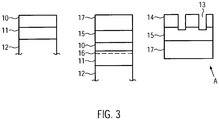
- the strained material islands 14 are separated by the buried material 15, structure A shown in Figure 1 results, if the step of patterning the buried layer 15 is performed after the transfer of the strained material islands 14 to the first support substrate 17 (see Figure 3 ).
- the strained material layer 10 grown on the seed layer 11 formed atop of the substrate 12 is bonded via the buried layer 15 to the support substrate 17 and ion implantation down to the strained material layer 10 or the seed layer 11 results in a weakened layer 16 with a rather homogeneous implantation profile (depth) thereby facilitating accurate detachment.
- trenches 13 are etched with depths of at least the thickness of the strained material layer 10.
- the trenches can be formed through the buried layer 15 down to the first support substrate 17.
- a second buried layer reference sign 18 of Figure 2
- the step of patterning of the strained material layer 10 may be carried out even later in the sequence of processing steps. Patterning after the deposition of the second buried layer 18 results in bonding of individual strained material islands to the second support substrate.
- Heat treatment is then performed for the double layer stack consisting of the material of the seed layer 11 and the strained material layer 10 atop the compliant layer 15. Subsequent final removal of the material of the seed layer 11 may be accompanied by an additional annealing step to finish complete relaxation.
- the seed layer 11 may be partially etched and the heat treatment may be carried out several times in sequence prior to the final removal of residuals of the seed layer material 11 that, in this case, functions as a stiffening means to further avoid buckling.
- heat treatment is performed for the entire structure comprising the first support substrate 17, the first buried layer 15, the strained material islands 14, the second buried (that may also be compliant layer) 18 and the second support substrate 19 (see Figure 2 ).
- the second substrate 19, in this case, is providing a stiffening effect in order to further avoid buckling of the strained material islands 14, which proves particularly advantageous for relatively large island sizes (e.g., 1 mm x 1 mm and more).
- the seed layer 11 is GaN deposited on a sapphire substrate, detachment by laser lift off at the interface of the GaN layer and the sapphire substrate may also be performed during the process of transfer of the strained material islands.
- the support substrate 17 advantageously is a silicon substrate to obtain similar coefficients of thermal expansion thermal treatment.
- a strained InGaN - layer comprising 5 - 7 % indium and of a thickness of about 100 nm is formed by heteroepitaxy on a GaN seed layer deposited on a sapphire seed substrate (corresponding to reference sign 12 of Figure 2 ).
- a compliant layer of borophosphosilicate glass of a thickness of about 500 nm is subsequently formed on the oxide layer.
- the compliant layer comprises 4.5 % of boron and 2 % of phosphorous to achieve the desired relaxing effect.
- Hydrogen ion implantation is performed through the free surface of the compliant layer in order to form a weakened layer in the GaN seed layer and then the surface is polished, for example, by a CMP technique. Ion implantation is carried out with 4e17 atoms/cm2 and ion energies (about 120 keV) sufficient to pass through the compliant layer, the oxide layer and the InGaN layer.
- An absorbing layer of SixNy:H and of a thickness of about 150 nm is deposited on another sapphire substrate (corresponding to reference sign 17 of Figure 2 ) and a bonding layer of borophosphosilicate glass is subsequently formed on the nitride layer and polished prior to bonding to the weakened structure including the InGaN strain layer.
- the resulting entire borophosphosilicate glass layer has a thickness of about 1 micrometer.
- fracture at the weakened layer and detachment of the initial sapphire seed layer together with the seed layer of GaN is achieved by thermal treatment at 450 °C for 10 hours. Note, that at this stage the temperature is kept below the melting (reflow) temperature of the borophosphosilicate glass layer.
- the residual GaN seed material is dry etched to free the InGaN layer of N polarity.
- the InGaN layer is subsequently patterned to form trenches of 1 depths of 10 - 40 nm in the borophosphosilicate glass layer by a standard lithography process.
- annealing treatment is performed at 800 °C for 4 hours to cause reflow of the borophosphosilicate glass layer and the corresponding relaxation of the strained InGaN islands (of about 1002 to 3002 micrometers2) resulting from the patterning process.
- An SiN layer of a thickness of about 50 nm might be provided between the N face of the InGaN layer and the oxide layer of SiO2 (or an undoped-silicon-glass) to improve adherence between the InGaN layer and the oxide layer.
- the SiN layer functions as an absorbing layer that might be used for a detachment step.
- An undoped-silicon-glass layer of a thickness of about 1 micrometer is deposited on a second sapphire substrate (corresponding to reference sign 19 of Figure 2 ).
- the combination of undoped-silicon-glass layers and the optional SiN layer form at least part of the buried layer 18 of Figure 2 .
- polishing of the bonding surfaces is performed before bonding of the undoped-silicon-glass layers.
- the entire thickness of the bonded undoped-silicon-glass layer may be about 1 micrometer (after polishing).
- Detachment of the substrate to which the InGaN strain layer formed by heteroepitaxy was transferred in the first transfer step is achieved by electromagnetic irradiation by means of an Ar/F laser providing light of 193 nm through the substrate that is transparent for that wavelength. Residuals of the SiN, undoped-silicon-glass and borophosphosilicate glass layers are subsequently removed by polishing and etching.
- the resulting structure comprising completely relaxed InGaN islands of gallium polarity can be used for the homoepitaxial growth of material layers that are suitable for the manufacture of electronic, photovoltaic or opto-electronic devices.
- epitaxy of an InGaN material with the same or a comparable indium content as compared to the one of the relaxed InGaN islands can be performed.
Claims (7)
- Procédé de formation d'îlots de matériau contraint au moins partiellement détendus sur un substrat cible, comprenant les étapes effectuées à la suite consistant à
transférer une couche de matériau contraint depuis un substrat de germe jusqu'à un substrat intermédiaire (1), comprenant le dépôt d'une couche compatible (2) qui est une couche de faible viscosité sur la couche de matériau contraint et la liaison de la couche compatible (2) au substrat intermédiaire (1) ;
former des îlots de matériau contraint (3) à partir de la couche de matériau contraint en mettant en forme la couche de matériau contraint de sorte que les îlots de matériau contraint sont séparés par des espaces qui s'étendent jusqu'au substrat intermédiaire (1) de sorte qu'il ne reste pratiquement aucun matériau de la couche compatible (2) au fond des espaces ;
détendre au moins partiellement les îlots de matériau contraint (3) par un premier traitement thermique ayant pour résultat une déformation plastique et une refusion de la couche compatible (2) ; et
transférer les îlots de matériau contraint au moins partiellement détendus (3) sur un substrat cible (5). - Procédé selon la revendication 1, dans lequel l'étape de transfert des îlots de matériau contraint au moins partiellement détendus (3) sur le substrat cible (5) comprend le dépôt d'une autre couche compatible (4) qui est une couche de faible viscosité sur les îlots de matériau contraint partiellement détendus (3) et la liaison de l'autre couche compatible (4) au substrat cible (5) ; et comprenant en outre l'étape consistant à détendre les îlots de matériau contraint au moins partiellement détendus (3) transférés sur le substrat cible (5) par un second traitement thermique.
- Procédé selon l'une des revendications 1 à 2, comprenant en outre les étapes consistant à
faire croître la couche de matière contraint sur un substrat de germe ;
implanter des ions dans le substrat de germe en dessous du matériau contraint pour former une couche affaiblie ; et
détacher le matériau contraint du substrat de germe au niveau de la couche affaiblie par un autre traitement thermique. - Procédé selon l'une des revendications précédentes, dans lequel le substrat de germe et le substrat intermédiaire et/ou le substrat intermédiaire et le substrat cible sont constitués du même matériau, en particulier, comprenant du saphir, du silicium, SiC, ou Ge.
- Procédé selon l'une des revendications précédentes, dans lequel la couche compatible (2) comprend une couche d'absorption appropriée pour absorber un rayonnement électromagnétique.
- Procédé selon l'une des revendications précédentes, dans lequel la couche de matériau contraint comprend ou est constituée d'InGaN et/ou la couche compatible (2) comprend ou est constituée de verre de borophosphosilicate, BPSG, ou d'un composé de SiO2 - comprenant du bore ou du phosphore.
- Procédé de fabrication d'un dispositif à semi-conducteur, consistant à fournir un matériau contraint au moins partiellement détendu (3) sur un substrat cible (5) selon l'une des revendications précédentes, et comprenant en outre une croissance épitaxiale d'au moins une couche de matériau sur le matériau contraint au moins partiellement détendu formé, en particulier, des couches pour des couches de dispositif LED ou photovoltaïque ou laser.
Priority Applications (11)
| Application Number | Priority Date | Filing Date | Title |
|---|---|---|---|
| EP08290759.3A EP2151852B1 (fr) | 2008-08-06 | 2008-08-06 | Relâchement et transfert de couches tendues |
| PCT/IB2008/003101 WO2010015878A2 (fr) | 2008-08-06 | 2008-09-08 | Procédé de modification d’un substrat |
| US12/341,852 US7981767B2 (en) | 2008-08-06 | 2008-12-22 | Methods for relaxation and transfer of strained layers and structures fabricated thereby |
| KR1020117003843A KR20110031988A (ko) | 2008-08-06 | 2009-07-02 | 변형된 층의 이완 및 이동 |
| CN2009801304478A CN102113090B (zh) | 2008-08-06 | 2009-07-02 | 应变层的松弛与转移 |
| KR1020137012250A KR101516619B1 (ko) | 2008-08-06 | 2009-07-02 | 물질 아일랜드 형성 방법, 그 물질 아일랜드를 이용한 반도체 소자 제조 방법 및 그 웨이퍼 |
| JP2011521447A JP5499371B2 (ja) | 2008-08-06 | 2009-07-02 | 歪み層の弛緩及び転写 |
| PCT/EP2009/004792 WO2010015302A2 (fr) | 2008-08-06 | 2009-07-02 | Relaxation et transfert de couches étirées |
| TW098124932A TWI456660B (zh) | 2008-08-06 | 2009-07-23 | 應變層的鬆弛及轉移 |
| TW098125948A TW201029049A (en) | 2008-08-06 | 2009-07-31 | Process for modifying a substrate |
| US13/081,788 US8492244B2 (en) | 2008-08-06 | 2011-04-07 | Methods for relaxation and transfer of strained layers and structures fabricated thereby |
Applications Claiming Priority (1)
| Application Number | Priority Date | Filing Date | Title |
|---|---|---|---|
| EP08290759.3A EP2151852B1 (fr) | 2008-08-06 | 2008-08-06 | Relâchement et transfert de couches tendues |
Publications (2)
| Publication Number | Publication Date |
|---|---|
| EP2151852A1 EP2151852A1 (fr) | 2010-02-10 |
| EP2151852B1 true EP2151852B1 (fr) | 2020-01-15 |
Family
ID=40427844
Family Applications (1)
| Application Number | Title | Priority Date | Filing Date |
|---|---|---|---|
| EP08290759.3A Active EP2151852B1 (fr) | 2008-08-06 | 2008-08-06 | Relâchement et transfert de couches tendues |
Country Status (7)
| Country | Link |
|---|---|
| US (2) | US7981767B2 (fr) |
| EP (1) | EP2151852B1 (fr) |
| JP (1) | JP5499371B2 (fr) |
| KR (2) | KR20110031988A (fr) |
| CN (1) | CN102113090B (fr) |
| TW (1) | TWI456660B (fr) |
| WO (1) | WO2010015302A2 (fr) |
Cited By (2)
| Publication number | Priority date | Publication date | Assignee | Title |
|---|---|---|---|---|
| US11295950B2 (en) | 2016-09-29 | 2022-04-05 | Soitec | Structure comprising single-crystal semiconductor islands and process for making such a structure |
| US11876073B2 (en) | 2018-11-08 | 2024-01-16 | Soitec | Process for collectively fabricating a plurality of semiconductor structures |
Families Citing this family (34)
| Publication number | Priority date | Publication date | Assignee | Title |
|---|---|---|---|---|
| US7018909B2 (en) * | 2003-02-28 | 2006-03-28 | S.O.I.Tec Silicon On Insulator Technologies S.A. | Forming structures that include a relaxed or pseudo-relaxed layer on a substrate |
| TWI457984B (zh) | 2008-08-06 | 2014-10-21 | Soitec Silicon On Insulator | 應變層的鬆弛方法 |
| EP2151856A1 (fr) * | 2008-08-06 | 2010-02-10 | S.O.I. TEC Silicon | Relâchement de couches tendues |
| EP2159836B1 (fr) | 2008-08-25 | 2017-05-31 | Soitec | Couches de durcissement pour le relâchement de couches contraintes |
| EP2221853B1 (fr) * | 2009-02-19 | 2012-04-25 | S.O.I. TEC Silicon | Relaxation et transfert de couches de matériaux sous contrainte |
| KR20120041237A (ko) | 2009-08-04 | 2012-04-30 | 갠 시스템즈 인크. | 아일랜드 매트릭스 갈륨 나이트라이드 마이크로파 및 전력 트랜지스터 |
| US9818857B2 (en) | 2009-08-04 | 2017-11-14 | Gan Systems Inc. | Fault tolerant design for large area nitride semiconductor devices |
| US9029866B2 (en) | 2009-08-04 | 2015-05-12 | Gan Systems Inc. | Gallium nitride power devices using island topography |
| US8791508B2 (en) | 2010-04-13 | 2014-07-29 | Gan Systems Inc. | High density gallium nitride devices using island topology |
| FR2973157B1 (fr) | 2011-03-25 | 2014-03-14 | Soitec Silicon On Insulator | Procédé de réalisation d'ilots de matériau contraint au moins partiellement relaxe |
| FR2975222A1 (fr) * | 2011-05-10 | 2012-11-16 | Soitec Silicon On Insulator | Procede de fabrication d'un substrat semiconducteur |
| FR2977069B1 (fr) | 2011-06-23 | 2014-02-07 | Soitec Silicon On Insulator | Procede de fabrication d'une structure semi-conductrice mettant en oeuvre un collage temporaire |
| FR2985609B1 (fr) | 2012-01-05 | 2014-02-07 | Commissariat Energie Atomique | Substrat structure pour leds a forte extraction de lumiere |
| WO2013114152A1 (fr) | 2012-01-31 | 2013-08-08 | Soitec | Dispositifs photoactifs à distribution améliorée des porteurs de charges, ainsi que leur procédé de formation. |
| US8471243B1 (en) | 2012-01-31 | 2013-06-25 | Soitec | Photoactive devices with improved distribution of charge carriers, and methods of forming same |
| US9583364B2 (en) | 2012-12-31 | 2017-02-28 | Sunedison Semiconductor Limited (Uen201334164H) | Processes and apparatus for preparing heterostructures with reduced strain by radial compression |
| US9620626B2 (en) | 2014-05-08 | 2017-04-11 | Soitec | Method for fabricating a semiconductor device including fin relaxation, and related structures |
| US9219150B1 (en) | 2014-09-18 | 2015-12-22 | Soitec | Method for fabricating semiconductor structures including fin structures with different strain states, and related semiconductor structures |
| US9165945B1 (en) | 2014-09-18 | 2015-10-20 | Soitec | Method for fabricating semiconductor structures including transistor channels having different strain states, and related semiconductor structures |
| US9209301B1 (en) | 2014-09-18 | 2015-12-08 | Soitec | Method for fabricating semiconductor layers including transistor channels having different strain states, and related semiconductor layers |
| FR3041364B1 (fr) * | 2015-09-18 | 2017-10-06 | Soitec Silicon On Insulator | Procede de transfert de paves monocristallins |
| WO2017142877A1 (fr) * | 2016-02-16 | 2017-08-24 | Glo Ab | Procédé de transfert sélectif de puce de led à une carte de fond de panier en utilisant des structures de liaison commandées en hauteur |
| FR3063571B1 (fr) * | 2017-03-01 | 2021-04-30 | Soitec Silicon On Insulator | Procede de fabrication d'un substrat donneur pour la formation de dispositifs optoelectroniques, collection de substrats issus de ce procede |
| EP4033531B1 (fr) | 2017-03-17 | 2023-08-02 | Soitec | Procédé de fabrication d'une pluralité d'îlots semiconducteurs cristallins |
| FR3064108B1 (fr) | 2017-03-17 | 2022-12-30 | Soitec Silicon On Insulator | Substrat de croissance pour la formation de dispositifs optoelectroniques, procede de fabrication d'un tel susbstrat, et utilisation du susbtrat notamment dans le domaine des micro-ecrans d'affichage |
| FR3079070B1 (fr) | 2018-03-13 | 2020-02-28 | Soitec | Procede de fabrication d'une pluralite d'ilots semi-conducteurs cristallins presentant une variete de parametres de maille |
| FR3079071B1 (fr) * | 2018-03-13 | 2020-02-28 | Soitec | Procede de fabrication d'une pluralite d'ilots semi-conducteurs cristallins prensentant une variete de parametres de maille |
| US11342479B2 (en) * | 2018-09-11 | 2022-05-24 | Facebook Technologies, Llc | Reducing bowing of materials before wafer-to-wafer bonding for LED manufacturing |
| US11145786B2 (en) | 2018-09-11 | 2021-10-12 | Facebook Technologies, Llc | Methods for wafer-to-wafer bonding |
| US11056611B2 (en) | 2018-09-11 | 2021-07-06 | Facebook Technologies, Llc | Mesa formation for wafer-to-wafer bonding |
| FR3091005B1 (fr) | 2018-12-21 | 2021-01-29 | Soitec Silicon On Insulator | Substrat de croissance et procede de fabrication d’un tel substrat |
| GB2586862B (en) | 2019-09-06 | 2021-12-15 | Plessey Semiconductors Ltd | LED precursor incorporating strain relaxing structure |
| FR3103627B1 (fr) | 2019-11-25 | 2023-03-24 | Soitec Silicon On Insulator | Procede de production d'un substrat comprenant une etape de traitement thermique de relaxation |
| GB2592253A (en) * | 2020-02-21 | 2021-08-25 | Rockley Photonics Ltd | Transfer die for micro-transfer printing |
Citations (1)
| Publication number | Priority date | Publication date | Assignee | Title |
|---|---|---|---|---|
| US20070228472A1 (en) * | 2003-11-19 | 2007-10-04 | International Business Machines Corporation | Silicon device on si: c-oi and sgoi and method of manufacture |
Family Cites Families (42)
| Publication number | Priority date | Publication date | Assignee | Title |
|---|---|---|---|---|
| US4994867A (en) * | 1988-07-22 | 1991-02-19 | Xerox Corporation | Intermediate buffer films with low plastic deformation threshold for lattice mismatched heteroepitaxy |
| JP3237888B2 (ja) * | 1992-01-31 | 2001-12-10 | キヤノン株式会社 | 半導体基体及びその作製方法 |
| US5461243A (en) | 1993-10-29 | 1995-10-24 | International Business Machines Corporation | Substrate for tensilely strained semiconductor |
| US5391257A (en) * | 1993-12-10 | 1995-02-21 | Rockwell International Corporation | Method of transferring a thin film to an alternate substrate |
| EP1758169A3 (fr) | 1996-08-27 | 2007-05-23 | Seiko Epson Corporation | Méthode de séparation, procédé de transfert d'un dispositif à film mince, et dispositif d'affichage à cristaux liquides obtenu par application du procédé de transfert |
| JP3744155B2 (ja) * | 1997-11-07 | 2006-02-08 | 豊田合成株式会社 | 窒化ガリウム系化合物半導体基板の製造方法 |
| FR2774511B1 (fr) * | 1998-01-30 | 2002-10-11 | Commissariat Energie Atomique | Substrat compliant en particulier pour un depot par hetero-epitaxie |
| FR2775121B1 (fr) | 1998-02-13 | 2000-05-05 | Picogiga Sa | Procede de fabrication de substrats en film mince de materiau semiconducteur, structures epitaxiales de materiau semiconducteur formees sur de tels substrats, et composants obtenus a partir de ces structures |
| US6406795B1 (en) * | 1998-11-25 | 2002-06-18 | Applied Optoelectronics, Inc. | Compliant universal substrates for optoelectronic and electronic devices |
| US6214733B1 (en) * | 1999-11-17 | 2001-04-10 | Elo Technologies, Inc. | Process for lift off and handling of thin film materials |
| JP2004507084A (ja) * | 2000-08-16 | 2004-03-04 | マサチューセッツ インスティテュート オブ テクノロジー | グレーデッドエピタキシャル成長を用いた半導体品の製造プロセス |
| US6524935B1 (en) * | 2000-09-29 | 2003-02-25 | International Business Machines Corporation | Preparation of strained Si/SiGe on insulator by hydrogen induced layer transfer technique |
| FR2817394B1 (fr) * | 2000-11-27 | 2003-10-31 | Soitec Silicon On Insulator | Procede de fabrication d'un substrat notamment pour l'optique, l'electronique ou l'optoelectronique et substrat obtenu par ce procede |
| US20030064535A1 (en) * | 2001-09-28 | 2003-04-03 | Kub Francis J. | Method of manufacturing a semiconductor device having a thin GaN material directly bonded to an optimized substrate |
| US6562127B1 (en) * | 2002-01-16 | 2003-05-13 | The United States Of America As Represented By The Secretary Of The Navy | Method of making mosaic array of thin semiconductor material of large substrates |
| US7175704B2 (en) | 2002-06-27 | 2007-02-13 | Diamond Innovations, Inc. | Method for reducing defect concentrations in crystals |
| US20040192067A1 (en) * | 2003-02-28 | 2004-09-30 | Bruno Ghyselen | Method for forming a relaxed or pseudo-relaxed useful layer on a substrate |
| US7018909B2 (en) * | 2003-02-28 | 2006-03-28 | S.O.I.Tec Silicon On Insulator Technologies S.A. | Forming structures that include a relaxed or pseudo-relaxed layer on a substrate |
| FR2851847B1 (fr) | 2003-02-28 | 2005-10-14 | Soitec Silicon On Insulator | Relaxation d'une couche mince apres transfert |
| US7348260B2 (en) * | 2003-02-28 | 2008-03-25 | S.O.I.Tec Silicon On Insulator Technologies | Method for forming a relaxed or pseudo-relaxed useful layer on a substrate |
| US7812340B2 (en) * | 2003-06-13 | 2010-10-12 | International Business Machines Corporation | Strained-silicon-on-insulator single-and double-gate MOSFET and method for forming the same |
| FR2860248B1 (fr) * | 2003-09-26 | 2006-02-17 | Centre Nat Rech Scient | Procede de realisation de substrats autosupportes de nitrures d'elements iii par hetero-epitaxie sur une couche sacrificielle |
| FR2860249B1 (fr) | 2003-09-30 | 2005-12-09 | Michel Bruel | Procede de fabrication d'une structure en forme de plaque, en particulier en silicium, application de procede, et structure en forme de plaque, en particulier en silicium |
| JP2006156950A (ja) * | 2004-10-29 | 2006-06-15 | Sharp Corp | 半導体発光素子の製造方法 |
| US7585792B2 (en) * | 2005-02-09 | 2009-09-08 | S.O.I.Tec Silicon On Insulator Technologies | Relaxation of a strained layer using a molten layer |
| EP1894234B1 (fr) * | 2005-02-28 | 2021-11-03 | Silicon Genesis Corporation | Procédé de rigidification du substrat et système pour un transfert de couche. |
| US7273798B2 (en) * | 2005-08-01 | 2007-09-25 | Avago Technologies Ecbu Ip (Singapore) Pte. Ltd. | Gallium nitride device substrate containing a lattice parameter altering element |
| US7399686B2 (en) * | 2005-09-01 | 2008-07-15 | International Business Machines Corporation | Method and apparatus for making coplanar dielectrically-isolated regions of different semiconductor materials on a substrate |
| US20070069225A1 (en) * | 2005-09-27 | 2007-03-29 | Lumileds Lighting U.S., Llc | III-V light emitting device |
| US8334155B2 (en) * | 2005-09-27 | 2012-12-18 | Philips Lumileds Lighting Company Llc | Substrate for growing a III-V light emitting device |
| FR2895420B1 (fr) | 2005-12-27 | 2008-02-22 | Tracit Technologies Sa | Procede de fabrication d'une structure demontable en forme de plaque, en particulier en silicium, et application de ce procede. |
| FR2895562B1 (fr) * | 2005-12-27 | 2008-03-28 | Commissariat Energie Atomique | Procede de relaxation d'une couche mince contrainte |
| JP2007281257A (ja) * | 2006-04-07 | 2007-10-25 | Toyoda Gosei Co Ltd | Iii族窒化物半導体発光素子 |
| JP5160080B2 (ja) | 2006-06-23 | 2013-03-13 | アイメック | 歪マルチゲートトランジスタの製造方法およびそこから得られるデバイス |
| US7494902B2 (en) * | 2006-06-23 | 2009-02-24 | Interuniversitair Microelektronica Centrum Vzw (Imec) | Method of fabricating a strained multi-gate transistor |
| JP5003033B2 (ja) * | 2006-06-30 | 2012-08-15 | 住友電気工業株式会社 | GaN薄膜貼り合わせ基板およびその製造方法、ならびにGaN系半導体デバイスおよびその製造方法 |
| EP1901345A1 (fr) | 2006-08-30 | 2008-03-19 | Siltronic AG | Galette semiconductrice multicouches et procédé de fabrication correspondant. |
| CA2669228C (fr) * | 2006-11-15 | 2014-12-16 | The Regents Of The University Of California | Procede pour une croissance heteroepitaxiale de gan, inn, et ain a face n de haute qualite et pour leurs alliages par un depot chimique en phase vapeur organique de metal |
| US20080122061A1 (en) * | 2006-11-29 | 2008-05-29 | Texas Instruments Incorporated | Semiconductor chip embedded in an insulator and having two-way heat extraction |
| US7858995B2 (en) * | 2007-08-03 | 2010-12-28 | Rohm Co., Ltd. | Semiconductor light emitting device |
| EP2151856A1 (fr) * | 2008-08-06 | 2010-02-10 | S.O.I. TEC Silicon | Relâchement de couches tendues |
| EP2151861A1 (fr) * | 2008-08-06 | 2010-02-10 | S.O.I. TEC Silicon | Passivation de structures semiconductrices gravées |
-
2008
- 2008-08-06 EP EP08290759.3A patent/EP2151852B1/fr active Active
- 2008-12-22 US US12/341,852 patent/US7981767B2/en active Active
-
2009
- 2009-07-02 KR KR1020117003843A patent/KR20110031988A/ko active Application Filing
- 2009-07-02 WO PCT/EP2009/004792 patent/WO2010015302A2/fr active Application Filing
- 2009-07-02 CN CN2009801304478A patent/CN102113090B/zh active Active
- 2009-07-02 KR KR1020137012250A patent/KR101516619B1/ko active IP Right Grant
- 2009-07-02 JP JP2011521447A patent/JP5499371B2/ja active Active
- 2009-07-23 TW TW098124932A patent/TWI456660B/zh active
-
2011
- 2011-04-07 US US13/081,788 patent/US8492244B2/en active Active
Patent Citations (1)
| Publication number | Priority date | Publication date | Assignee | Title |
|---|---|---|---|---|
| US20070228472A1 (en) * | 2003-11-19 | 2007-10-04 | International Business Machines Corporation | Silicon device on si: c-oi and sgoi and method of manufacture |
Non-Patent Citations (2)
| Title |
|---|
| HOBART K D ET AL: "Compliant substrates: a comparative study of the relaxation mechanisms of strained films bonded to high and low viscosity oxides", JOURNAL OF ELECTRONIC MATERIALS, WARRENDALE, PA, US, vol. 29, no. 7, 1 July 2000 (2000-07-01), pages 897 - 900, XP002565241, ISSN: 0361-5235, DOI: 10.1007/S11664-000-0177-2 * |
| YIN H ET AL: "Strain relaxation of SiGe islands on compliant oxide", JOURNAL OF APPLIED PHYSICS, AMERICAN INSTITUTE OF PHYSICS, US, vol. 91, no. 12, 15 June 2002 (2002-06-15), pages 9716 - 9722, XP012055487, ISSN: 0021-8979, DOI: 10.1063/1.1479757 * |
Cited By (2)
| Publication number | Priority date | Publication date | Assignee | Title |
|---|---|---|---|---|
| US11295950B2 (en) | 2016-09-29 | 2022-04-05 | Soitec | Structure comprising single-crystal semiconductor islands and process for making such a structure |
| US11876073B2 (en) | 2018-11-08 | 2024-01-16 | Soitec | Process for collectively fabricating a plurality of semiconductor structures |
Also Published As
| Publication number | Publication date |
|---|---|
| US20110180911A1 (en) | 2011-07-28 |
| US7981767B2 (en) | 2011-07-19 |
| US20100032793A1 (en) | 2010-02-11 |
| US8492244B2 (en) | 2013-07-23 |
| KR20110031988A (ko) | 2011-03-29 |
| KR20130070652A (ko) | 2013-06-27 |
| JP2011530179A (ja) | 2011-12-15 |
| KR101516619B1 (ko) | 2015-05-04 |
| TW201021125A (en) | 2010-06-01 |
| WO2010015302A2 (fr) | 2010-02-11 |
| JP5499371B2 (ja) | 2014-05-21 |
| WO2010015302A3 (fr) | 2010-05-14 |
| CN102113090A (zh) | 2011-06-29 |
| TWI456660B (zh) | 2014-10-11 |
| EP2151852A1 (fr) | 2010-02-10 |
| CN102113090B (zh) | 2013-12-18 |
Similar Documents
| Publication | Publication Date | Title |
|---|---|---|
| EP2151852B1 (fr) | Relâchement et transfert de couches tendues | |
| EP2151856A1 (fr) | Relâchement de couches tendues | |
| US8481407B2 (en) | Processes for fabricating heterostructures | |
| KR20120094050A (ko) | 글라스 접합층을 이용한 반도체 구조들 및 디바이스들의 제조 방법들 및 이와 같은 방법들에 의해 형성되는 반도체 구조들 및 디바이스들 | |
| CN103123895B (zh) | 应变层的松弛 | |
| US9041165B2 (en) | Relaxation and transfer of strained material layers | |
| US8785293B2 (en) | Adaptation of the lattice parameter of a layer of strained material | |
| US8642443B2 (en) | Process for the realization of islands of at least partially relaxed strained material | |
| US8912081B2 (en) | Stiffening layers for the relaxation of strained layers |
Legal Events
| Date | Code | Title | Description |
|---|---|---|---|
| PUAI | Public reference made under article 153(3) epc to a published international application that has entered the european phase |
Free format text: ORIGINAL CODE: 0009012 |
|
| AK | Designated contracting states |
Kind code of ref document: A1 Designated state(s): AT BE BG CH CY CZ DE DK EE ES FI FR GB GR HR HU IE IS IT LI LT LU LV MC MT NL NO PL PT RO SE SI SK TR |
|
| AX | Request for extension of the european patent |
Extension state: AL BA MK RS |
|
| 17P | Request for examination filed |
Effective date: 20100701 |
|
| 17Q | First examination report despatched |
Effective date: 20100803 |
|
| AKX | Designation fees paid |
Designated state(s): AT BE BG CH CY CZ DE DK EE ES FI FR GB GR HR HU IE IS IT LI LT LU LV MC MT NL NO PL PT RO SE SI SK TR |
|
| RAP1 | Party data changed (applicant data changed or rights of an application transferred) |
Owner name: SOITEC |
|
| STAA | Information on the status of an ep patent application or granted ep patent |
Free format text: STATUS: EXAMINATION IS IN PROGRESS |
|
| GRAP | Despatch of communication of intention to grant a patent |
Free format text: ORIGINAL CODE: EPIDOSNIGR1 |
|
| STAA | Information on the status of an ep patent application or granted ep patent |
Free format text: STATUS: GRANT OF PATENT IS INTENDED |
|
| INTG | Intention to grant announced |
Effective date: 20190823 |
|
| GRAS | Grant fee paid |
Free format text: ORIGINAL CODE: EPIDOSNIGR3 |
|
| GRAA | (expected) grant |
Free format text: ORIGINAL CODE: 0009210 |
|
| STAA | Information on the status of an ep patent application or granted ep patent |
Free format text: STATUS: THE PATENT HAS BEEN GRANTED |
|
| AK | Designated contracting states |
Kind code of ref document: B1 Designated state(s): AT BE BG CH CY CZ DE DK EE ES FI FR GB GR HR HU IE IS IT LI LT LU LV MC MT NL NO PL PT RO SE SI SK TR |
|
| REG | Reference to a national code |
Ref country code: GB Ref legal event code: FG4D Ref country code: CH Ref legal event code: EP |
|
| REG | Reference to a national code |
Ref country code: IE Ref legal event code: FG4D |
|
| REG | Reference to a national code |
Ref country code: DE Ref legal event code: R096 Ref document number: 602008062006 Country of ref document: DE |
|
| REG | Reference to a national code |
Ref country code: AT Ref legal event code: REF Ref document number: 1225894 Country of ref document: AT Kind code of ref document: T Effective date: 20200215 |
|
| REG | Reference to a national code |
Ref country code: NL Ref legal event code: MP Effective date: 20200115 |
|
| REG | Reference to a national code |
Ref country code: LT Ref legal event code: MG4D |
|
| PG25 | Lapsed in a contracting state [announced via postgrant information from national office to epo] |
Ref country code: NO Free format text: LAPSE BECAUSE OF FAILURE TO SUBMIT A TRANSLATION OF THE DESCRIPTION OR TO PAY THE FEE WITHIN THE PRESCRIBED TIME-LIMIT Effective date: 20200415 Ref country code: PT Free format text: LAPSE BECAUSE OF FAILURE TO SUBMIT A TRANSLATION OF THE DESCRIPTION OR TO PAY THE FEE WITHIN THE PRESCRIBED TIME-LIMIT Effective date: 20200607 Ref country code: NL Free format text: LAPSE BECAUSE OF FAILURE TO SUBMIT A TRANSLATION OF THE DESCRIPTION OR TO PAY THE FEE WITHIN THE PRESCRIBED TIME-LIMIT Effective date: 20200115 Ref country code: FI Free format text: LAPSE BECAUSE OF FAILURE TO SUBMIT A TRANSLATION OF THE DESCRIPTION OR TO PAY THE FEE WITHIN THE PRESCRIBED TIME-LIMIT Effective date: 20200115 |
|
| PG25 | Lapsed in a contracting state [announced via postgrant information from national office to epo] |
Ref country code: LV Free format text: LAPSE BECAUSE OF FAILURE TO SUBMIT A TRANSLATION OF THE DESCRIPTION OR TO PAY THE FEE WITHIN THE PRESCRIBED TIME-LIMIT Effective date: 20200115 Ref country code: SE Free format text: LAPSE BECAUSE OF FAILURE TO SUBMIT A TRANSLATION OF THE DESCRIPTION OR TO PAY THE FEE WITHIN THE PRESCRIBED TIME-LIMIT Effective date: 20200115 Ref country code: HR Free format text: LAPSE BECAUSE OF FAILURE TO SUBMIT A TRANSLATION OF THE DESCRIPTION OR TO PAY THE FEE WITHIN THE PRESCRIBED TIME-LIMIT Effective date: 20200115 Ref country code: IS Free format text: LAPSE BECAUSE OF FAILURE TO SUBMIT A TRANSLATION OF THE DESCRIPTION OR TO PAY THE FEE WITHIN THE PRESCRIBED TIME-LIMIT Effective date: 20200515 Ref country code: BG Free format text: LAPSE BECAUSE OF FAILURE TO SUBMIT A TRANSLATION OF THE DESCRIPTION OR TO PAY THE FEE WITHIN THE PRESCRIBED TIME-LIMIT Effective date: 20200415 Ref country code: GR Free format text: LAPSE BECAUSE OF FAILURE TO SUBMIT A TRANSLATION OF THE DESCRIPTION OR TO PAY THE FEE WITHIN THE PRESCRIBED TIME-LIMIT Effective date: 20200416 |
|
| REG | Reference to a national code |
Ref country code: DE Ref legal event code: R097 Ref document number: 602008062006 Country of ref document: DE |
|
| PG25 | Lapsed in a contracting state [announced via postgrant information from national office to epo] |
Ref country code: ES Free format text: LAPSE BECAUSE OF FAILURE TO SUBMIT A TRANSLATION OF THE DESCRIPTION OR TO PAY THE FEE WITHIN THE PRESCRIBED TIME-LIMIT Effective date: 20200115 Ref country code: CZ Free format text: LAPSE BECAUSE OF FAILURE TO SUBMIT A TRANSLATION OF THE DESCRIPTION OR TO PAY THE FEE WITHIN THE PRESCRIBED TIME-LIMIT Effective date: 20200115 Ref country code: RO Free format text: LAPSE BECAUSE OF FAILURE TO SUBMIT A TRANSLATION OF THE DESCRIPTION OR TO PAY THE FEE WITHIN THE PRESCRIBED TIME-LIMIT Effective date: 20200115 Ref country code: SK Free format text: LAPSE BECAUSE OF FAILURE TO SUBMIT A TRANSLATION OF THE DESCRIPTION OR TO PAY THE FEE WITHIN THE PRESCRIBED TIME-LIMIT Effective date: 20200115 Ref country code: LT Free format text: LAPSE BECAUSE OF FAILURE TO SUBMIT A TRANSLATION OF THE DESCRIPTION OR TO PAY THE FEE WITHIN THE PRESCRIBED TIME-LIMIT Effective date: 20200115 Ref country code: EE Free format text: LAPSE BECAUSE OF FAILURE TO SUBMIT A TRANSLATION OF THE DESCRIPTION OR TO PAY THE FEE WITHIN THE PRESCRIBED TIME-LIMIT Effective date: 20200115 Ref country code: DK Free format text: LAPSE BECAUSE OF FAILURE TO SUBMIT A TRANSLATION OF THE DESCRIPTION OR TO PAY THE FEE WITHIN THE PRESCRIBED TIME-LIMIT Effective date: 20200115 |
|
| REG | Reference to a national code |
Ref country code: AT Ref legal event code: MK05 Ref document number: 1225894 Country of ref document: AT Kind code of ref document: T Effective date: 20200115 |
|
| PLBE | No opposition filed within time limit |
Free format text: ORIGINAL CODE: 0009261 |
|
| STAA | Information on the status of an ep patent application or granted ep patent |
Free format text: STATUS: NO OPPOSITION FILED WITHIN TIME LIMIT |
|
| 26N | No opposition filed |
Effective date: 20201016 |
|
| PG25 | Lapsed in a contracting state [announced via postgrant information from national office to epo] |
Ref country code: AT Free format text: LAPSE BECAUSE OF FAILURE TO SUBMIT A TRANSLATION OF THE DESCRIPTION OR TO PAY THE FEE WITHIN THE PRESCRIBED TIME-LIMIT Effective date: 20200115 Ref country code: IT Free format text: LAPSE BECAUSE OF FAILURE TO SUBMIT A TRANSLATION OF THE DESCRIPTION OR TO PAY THE FEE WITHIN THE PRESCRIBED TIME-LIMIT Effective date: 20200115 |
|
| PG25 | Lapsed in a contracting state [announced via postgrant information from national office to epo] |
Ref country code: SI Free format text: LAPSE BECAUSE OF FAILURE TO SUBMIT A TRANSLATION OF THE DESCRIPTION OR TO PAY THE FEE WITHIN THE PRESCRIBED TIME-LIMIT Effective date: 20200115 Ref country code: PL Free format text: LAPSE BECAUSE OF FAILURE TO SUBMIT A TRANSLATION OF THE DESCRIPTION OR TO PAY THE FEE WITHIN THE PRESCRIBED TIME-LIMIT Effective date: 20200115 |
|
| PG25 | Lapsed in a contracting state [announced via postgrant information from national office to epo] |
Ref country code: MC Free format text: LAPSE BECAUSE OF FAILURE TO SUBMIT A TRANSLATION OF THE DESCRIPTION OR TO PAY THE FEE WITHIN THE PRESCRIBED TIME-LIMIT Effective date: 20200115 |
|
| REG | Reference to a national code |
Ref country code: CH Ref legal event code: PL |
|
| PG25 | Lapsed in a contracting state [announced via postgrant information from national office to epo] |
Ref country code: LU Free format text: LAPSE BECAUSE OF NON-PAYMENT OF DUE FEES Effective date: 20200806 Ref country code: LI Free format text: LAPSE BECAUSE OF NON-PAYMENT OF DUE FEES Effective date: 20200831 Ref country code: CH Free format text: LAPSE BECAUSE OF NON-PAYMENT OF DUE FEES Effective date: 20200831 |
|
| REG | Reference to a national code |
Ref country code: BE Ref legal event code: MM Effective date: 20200831 |
|
| PG25 | Lapsed in a contracting state [announced via postgrant information from national office to epo] |
Ref country code: BE Free format text: LAPSE BECAUSE OF NON-PAYMENT OF DUE FEES Effective date: 20200831 |
|
| PG25 | Lapsed in a contracting state [announced via postgrant information from national office to epo] |
Ref country code: TR Free format text: LAPSE BECAUSE OF FAILURE TO SUBMIT A TRANSLATION OF THE DESCRIPTION OR TO PAY THE FEE WITHIN THE PRESCRIBED TIME-LIMIT Effective date: 20200115 Ref country code: MT Free format text: LAPSE BECAUSE OF FAILURE TO SUBMIT A TRANSLATION OF THE DESCRIPTION OR TO PAY THE FEE WITHIN THE PRESCRIBED TIME-LIMIT Effective date: 20200115 Ref country code: CY Free format text: LAPSE BECAUSE OF FAILURE TO SUBMIT A TRANSLATION OF THE DESCRIPTION OR TO PAY THE FEE WITHIN THE PRESCRIBED TIME-LIMIT Effective date: 20200115 |
|
| PGFP | Annual fee paid to national office [announced via postgrant information from national office to epo] |
Ref country code: IE Payment date: 20230710 Year of fee payment: 16 Ref country code: GB Payment date: 20230706 Year of fee payment: 16 |
|
| PGFP | Annual fee paid to national office [announced via postgrant information from national office to epo] |
Ref country code: FR Payment date: 20230721 Year of fee payment: 16 Ref country code: DE Payment date: 20230705 Year of fee payment: 16 |