EP2117117B1 - Modulations-digital-analog-umsetzer, digitales signalverarbeitungsverfahren und av-einrichtung - Google Patents
Modulations-digital-analog-umsetzer, digitales signalverarbeitungsverfahren und av-einrichtung Download PDFInfo
- Publication number
- EP2117117B1 EP2117117B1 EP07860383.4A EP07860383A EP2117117B1 EP 2117117 B1 EP2117117 B1 EP 2117117B1 EP 07860383 A EP07860383 A EP 07860383A EP 2117117 B1 EP2117117 B1 EP 2117117B1
- Authority
- EP
- European Patent Office
- Prior art keywords
- compensation
- signal
- modulation
- digital
- input signal
- Prior art date
- Legal status (The legal status is an assumption and is not a legal conclusion. Google has not performed a legal analysis and makes no representation as to the accuracy of the status listed.)
- Not-in-force
Links
- 238000003672 processing method Methods 0.000 title claims description 6
- 230000006870 function Effects 0.000 claims description 146
- 238000000034 method Methods 0.000 claims description 46
- 238000001228 spectrum Methods 0.000 claims description 43
- 238000004458 analytical method Methods 0.000 claims description 19
- 238000011144 upstream manufacturing Methods 0.000 claims description 17
- NCGICGYLBXGBGN-UHFFFAOYSA-N 3-morpholin-4-yl-1-oxa-3-azonia-2-azanidacyclopent-3-en-5-imine;hydrochloride Chemical group Cl.[N-]1OC(=N)C=[N+]1N1CCOCC1 NCGICGYLBXGBGN-UHFFFAOYSA-N 0.000 description 22
- 101100042630 Caenorhabditis elegans sin-3 gene Proteins 0.000 description 21
- 230000015654 memory Effects 0.000 description 21
- 238000010586 diagram Methods 0.000 description 14
- 230000005236 sound signal Effects 0.000 description 11
- 239000011159 matrix material Substances 0.000 description 10
- 238000004364 calculation method Methods 0.000 description 8
- 238000006243 chemical reaction Methods 0.000 description 6
- 230000000694 effects Effects 0.000 description 6
- 230000003321 amplification Effects 0.000 description 5
- 238000003199 nucleic acid amplification method Methods 0.000 description 5
- 238000005259 measurement Methods 0.000 description 3
- 238000005070 sampling Methods 0.000 description 3
- 230000006866 deterioration Effects 0.000 description 2
- 238000012545 processing Methods 0.000 description 2
- 230000000717 retained effect Effects 0.000 description 2
- OVSKIKFHRZPJSS-UHFFFAOYSA-N 2,4-D Chemical compound OC(=O)COC1=CC=C(Cl)C=C1Cl OVSKIKFHRZPJSS-UHFFFAOYSA-N 0.000 description 1
- 230000003044 adaptive effect Effects 0.000 description 1
- 239000003990 capacitor Substances 0.000 description 1
- 238000009795 derivation Methods 0.000 description 1
- 238000011161 development Methods 0.000 description 1
- 238000002474 experimental method Methods 0.000 description 1
- 230000005669 field effect Effects 0.000 description 1
- 230000010354 integration Effects 0.000 description 1
- 229910044991 metal oxide Inorganic materials 0.000 description 1
- 150000004706 metal oxides Chemical class 0.000 description 1
- 238000013139 quantization Methods 0.000 description 1
- 229920006395 saturated elastomer Polymers 0.000 description 1
- 239000004065 semiconductor Substances 0.000 description 1
- 230000001629 suppression Effects 0.000 description 1
- 230000002123 temporal effect Effects 0.000 description 1
- 238000012546 transfer Methods 0.000 description 1
Images
Classifications
-
- H—ELECTRICITY
- H03—ELECTRONIC CIRCUITRY
- H03F—AMPLIFIERS
- H03F3/00—Amplifiers with only discharge tubes or only semiconductor devices as amplifying elements
- H03F3/20—Power amplifiers, e.g. Class B amplifiers, Class C amplifiers
- H03F3/21—Power amplifiers, e.g. Class B amplifiers, Class C amplifiers with semiconductor devices only
- H03F3/217—Class D power amplifiers; Switching amplifiers
- H03F3/2173—Class D power amplifiers; Switching amplifiers of the bridge type
-
- H—ELECTRICITY
- H03—ELECTRONIC CIRCUITRY
- H03M—CODING; DECODING; CODE CONVERSION IN GENERAL
- H03M3/00—Conversion of analogue values to or from differential modulation
- H03M3/30—Delta-sigma modulation
- H03M3/38—Calibration
- H03M3/386—Calibration over the full range of the converter, e.g. for correcting differential non-linearity
- H03M3/388—Calibration over the full range of the converter, e.g. for correcting differential non-linearity by storing corrected or correction values in one or more digital look-up tables
-
- H—ELECTRICITY
- H03—ELECTRONIC CIRCUITRY
- H03F—AMPLIFIERS
- H03F2200/00—Indexing scheme relating to amplifiers
- H03F2200/03—Indexing scheme relating to amplifiers the amplifier being designed for audio applications
-
- H—ELECTRICITY
- H03—ELECTRONIC CIRCUITRY
- H03F—AMPLIFIERS
- H03F2200/00—Indexing scheme relating to amplifiers
- H03F2200/331—Sigma delta modulation being used in an amplifying circuit
-
- H—ELECTRICITY
- H03—ELECTRONIC CIRCUITRY
- H03M—CODING; DECODING; CODE CONVERSION IN GENERAL
- H03M3/00—Conversion of analogue values to or from differential modulation
- H03M3/30—Delta-sigma modulation
- H03M3/50—Digital/analogue converters using delta-sigma modulation as an intermediate step
-
- H—ELECTRICITY
- H03—ELECTRONIC CIRCUITRY
- H03M—CODING; DECODING; CODE CONVERSION IN GENERAL
- H03M7/00—Conversion of a code where information is represented by a given sequence or number of digits to a code where the same, similar or subset of information is represented by a different sequence or number of digits
- H03M7/30—Compression; Expansion; Suppression of unnecessary data, e.g. redundancy reduction
- H03M7/3002—Conversion to or from differential modulation
- H03M7/3004—Digital delta-sigma modulation
- H03M7/3015—Structural details of digital delta-sigma modulators
- H03M7/302—Structural details of digital delta-sigma modulators characterised by the number of quantisers and their type and resolution
- H03M7/3024—Structural details of digital delta-sigma modulators characterised by the number of quantisers and their type and resolution having one quantiser only
- H03M7/3028—Structural details of digital delta-sigma modulators characterised by the number of quantisers and their type and resolution having one quantiser only the quantiser being a single bit one
-
- H—ELECTRICITY
- H03—ELECTRONIC CIRCUITRY
- H03M—CODING; DECODING; CODE CONVERSION IN GENERAL
- H03M7/00—Conversion of a code where information is represented by a given sequence or number of digits to a code where the same, similar or subset of information is represented by a different sequence or number of digits
- H03M7/30—Compression; Expansion; Suppression of unnecessary data, e.g. redundancy reduction
- H03M7/3002—Conversion to or from differential modulation
- H03M7/3004—Digital delta-sigma modulation
- H03M7/3015—Structural details of digital delta-sigma modulators
- H03M7/3031—Structural details of digital delta-sigma modulators characterised by the order of the loop filter, e.g. having a first order loop filter in the feedforward path
- H03M7/3033—Structural details of digital delta-sigma modulators characterised by the order of the loop filter, e.g. having a first order loop filter in the feedforward path the modulator having a higher order loop filter in the feedforward path, e.g. with distributed feedforward inputs
Definitions
- the present invention relates to: a ⁇ modulation digital-analogue converter; a digital signal processing method; and an AV device, each of which (i) controls switching of a D-Class amplifier according to a signal that has been encoded by ⁇ modulation, and (ii) outputs an analogue signal converted and amplified from an inputted digital signal.
- the ⁇ modulation has been employed in a D-Class amplifier which amplifies an input signal by switching a transistor.
- the D-Class amplifier operates while the transistor is in a nonlinear region (saturated region). Therefore, the D-Class amplifier has an advantage of being capable of amplifying electric power highly efficiently.
- the D-Class amplifier switches over constant voltages to each other in accordance with an input signal.
- the D-Class amplifier outputs a binary, that is, (i) a voltage corresponding to an input signal indicating "ON” and (ii) a voltage corresponding to an input signal indicating "OFF".
- the D-Class amplifier amplifies a binary input indicating "ON/OFF". Accordingly, for example, in a case where an audio signal is amplified by use of the D-Class amplifier, first, a binary signal indicating the audio signal is created. In other words, it is necessary to encode the audio signal into a one-bit signal. A method adopting the ⁇ modulation has been put into practical use in encoding the audio signal into the one-bit signal.
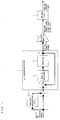
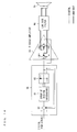
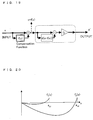
- Fig. 13 is a view illustrating an arrangement of a conventional ⁇ modulation one-bit amplifier.
- the ⁇ modulation D-Class amplifier includes a DA converter (DAC) 50, a subtractor 51, a group of analogue integrators 52, a quantizer 53, a D-Class amplifier 54, a low-pass filter 55, and a speaker 56.
- the ⁇ modulation one-bit amplifier amplifies an input signal that is encoded by PCM (Pulse Code Modulation), and outputs an analogue signal converted and amplified from the input signal.
- PCM Pulse Code Modulation
- the DAC 50 receives a digital signal that is encoded from an audio signal by the PCM.
- the DAC 50 converts the inputted digital signal into an analogue signal, and outputs the analogue signal to the subtractor 51. Further, a switching pulse that is outputted from the D-Class amplifier 54 is fed back to the subtractor 51. The switching pulse outputted from the D-Class amplifier 54, and the feedback will be described later more specifically.
- the subtractor 51 subtracts, from the analogue signal received from the DAC 50, the switching pulse that is fed back from the D-Class amplifier 54, so as to create a difference signal. Then, the subtractor 51 outputs the difference signal to the group of analogue integrators 52.
- the group of analogue integrators 52 integrates the difference signal received from the subtractor 51, and then outputs the difference signal to the quantizer 53.
- the quantizer 53 quantizes, at every predetermined sampling cycle, the input received from the group of analogue integrators 52, so as to create a binary quantized signal, i.e. "0" or "1". Then, the quantizer 53 outputs the quantized signal to the D-Class amplifier 54.
- the D-Class amplifier 54 carries out the switching in accordance with the quantized signal, so as to change over a constant voltage to another constant voltage. This generates a high-voltage switching pulse corresponding to the quantized signal, in other words, the quantized signal is amplified.
- the D-Class amplifier 54 outputs the switching pulse to the low-pass filter 55.
- the low-pass filter 55 smoothes the switching pulse so as to demodulate the switching pulse. Then, the low-pass filter 55 outputs, from the speaker 56, the switching pulse as such an analogue signal that an original audio signal is amplified.
- the ⁇ modulation one-bit amplifier includes a feedback loop which negatively feeds back, to the subtractor 51, the switching pulse outputted from the D-Class amplifier 54.
- This makes it possible to feed back, to the subtractor 51, analogue information (including power source fluctuation noise, a switching error component, and the like) which is included in the output of the D-Class amplifier 54.
- the power source fluctuation noise and the switching error component can be compensated so that an SNR (Signal to Noise Ratio) is improved and a "THD (Total Harmonic Distortion) +N (Noise)" is reduced.
- Fig. 14 is a view illustrating an arrangement of a conventional ⁇ modulation one-bit amplifier which does not include a feedback loop for feeding back the analogue information.
- This ⁇ modulation one-bit amplifier includes: a subtractor 60; a group of digital integrators 61; a quantizer 62; a D-Class amplifier 63; a low-pass filter 64; and a speaker 65.
- the subtractor 60, the group of the digital integrators 61, and the quantizer 62 constitute a ⁇ modulation section 66.
- This ⁇ modulation one-bit amplifier amplifies an input signal that has been digitally-encoded by the PCM, and then outputs an analogue signal thus prepared from the input signal. The following description deals with how each component of the ⁇ modulation one-bit amplifier is operated.
- the subtractor 60 receives a digital signal that has been encoded from an audio signal by the PCM. Further, a quantized signal outputted from the quantizer 62 is fed back to the subtractor 60. The quantized signal outputted from the quantizer 62, and the feedback will be described later more specifically.
- the subtractor 60 subtracts, from the input signal (that is, the digital signal that is encoded from an audio signal by the PCM), the quantized signal that is fed back from the quantizer 62, so as to create a difference signal. Then, the subtractor 60 outputs the difference signal to the group of digital integrators 61.
- the group of digital integrators 61 integrates the difference signal received from the subtractor 60, and then outputs the difference signal to the quantizer 62.
- the quantizer 62 quantizes, at every predetermined sampling cycle, the input received from the group of digital integrators 61, so as to create a binary quantized signal indicating "0" and "1". Then, the quantizer 62 outputs the quantized signal to the D-Class amplifier 63.
- the D-Class amplifier 63 carries out the switching in accordance with the quantized signal, so as to change over a constant voltage to another constant voltage. This generates a high-voltage switching pulse corresponding to the quantized signal, in other words, the quantized signal is amplified.
- the D-Class amplifier 63 outputs the switching pulse to the low-pass filter 64.
- the low-pass filter 64 smoothes and demodulates the switching pulse, and outputs an analogue signal from the speaker 65, the analogue signal thus prepared from the original audio signal.
- the ⁇ modulation section 66 includes a feedback loop for negatively feeding back, to the subtractor 60, the quantized signal outputted from the quantizer 62.
- Patent Literature 1 discloses a technique for suppressing harmonic distortion of a signal for driving the switching amplifier (D-Class amplifier).
- a PWM (Pulse Width Modulation) signal is created in such a manner that an inputted digital signal is quantized by a ⁇ converter, and then is subjected to PWM, and (ii) the switching amplifier is driven by the PWM signal.
- Harmonic distortion due to the PWM is estimated in advance, and suppressed by canceling out a component of the harmonic distortion.
- the estimation of the harmonic distortion in advance may be based on a linear combination of a product with the use of an original signal, and signals indicating first-order and second-order temporal differential signals of a continuous-time signal corresponding to the original input signal. At that time, a fundamental harmonic component which is generated due to a third-order distortion is taken into consideration.
- Patent Literature 2 discloses a technique in which, in a ⁇ digital-analogue converter and an output amplifying circuit, each of which includes a ⁇ conversion circuit, a PWM circuit, and a distortion compensation circuit, a second-order harmonic generated in the PWM circuit or a PWM signal received from the PWM circuit is inputted, so that generation of a second-order harmonic in a D-Class amplifier or the like is suppressed.
- JP 2004-088430 relates to a class D amplifier comprising a ⁇ modulating means.
- WO 2006/020503 relates to a digital adaptive feed forward harmonic distortion compensation device for a digitally controlled power stage.
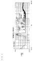
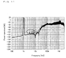
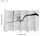
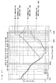
- Fig. 15 is a diagram showing a frequency spectrum of a signal and noise both of which are included in an output signal, in a case where a sine wave is inputted into a conventional ⁇ modulation D-Class amplifier.
- Fig. 15 shows a frequency spectrum obtained in such a manner that the output signal of the ⁇ modulation D-Class amplifier 63 is subjected to a frequency-analysis.
- the frequency spectrum in the vicinity of 1kHz shows a signal component of an amplified fundamental harmonic (sine wave).
- the output signal of the ⁇ modulation D-Class amplifier includes odd-order harmonic components of the fundamental harmonic in a human-audible frequency range (from 20Hz to 20kHz) so that the odd-order harmonic components can be heard by a human as noise.
- Patent Literature 1 With the arrangement disclosed in Patent Literature 1, it is possible to logically compensate harmonics generated in the conversion of the ⁇ modulation to the PWM.
- analogue factors of a switching amplifier that is, harmonics generated in the switching amplifier due to a dead time or a power source fluctuation, are not taken into consideration.
- distortion components higher than a third-order distortion component are also not taken into consideration.
- Patent Literature 1 does not disclose details of an effect of improving a distortion characteristic in accordance with an amplitude value of an input. Moreover, it is believed that even if the compensation is effective with respect to certain amplitude of an input signal, there is a case where the compensation is not effective with respect to other amplitude of the input signal.
- Patent Literature 2 does not take into consideration distortion components other than a second-order distortion component.
- Patent Literature 2 does not disclose details of the effect of improving the distortion characteristic in accordance with an amplitude value of an input. Further, it is believed that even if the compensation is effective with respect to certain amplitude of an input signal, there is a case where the compensation is not effective with respect to other amplitude of the input signal.
- An object of the present invention is to provide a ⁇ modulation digital-analogue converter which, with a simple circuit arrangement, suppresses not only generation of a third-order harmonic but also generation of odd-order (higher than third-order) harmonics while taking amplitude of an input into consideration, and thereby is excellent in SNR and THD+N.
- a ⁇ modulation digital-analogue converter of the present invention includes: ⁇ modulation means including integrating means including at least one integrator for integrating a digital signal, and quantizing means for modulating an output of the integrating means into a quantized signal, the ⁇ modulation means feeding back the quantized signal to an upstream of the integrating means; a switching amplifier for generating a switching pulse in accordance with the quantized signal; a low-pass filter for demodulating the switching pulse; storage means in which a first compensation function is stored in advance, the first compensation function indicating a correspondence relationship between each of a plurality of possible input values of an input signal which is externally supplied, and each of compensation values that are individually associated with the possible input values; and compensation means for compensating the input signal which is externally supplied, based on a compensation value associated with the input signal among the compensation values, and supplying to the ⁇ modulation means the input signal thus compensated; the first compensation function being set based on a spectrum of odd-order harmonics whose frequencies
- a digital signal processing method of the present invention employs a ⁇ modulation digital-analogue converter
- the ⁇ modulation digital-analogue converter including: ⁇ modulation means including integrating means including at least one integrator for integrating a digital signal, and quantizing means for modulating an output of the integrating means into a quantized signal, the ⁇ modulation means feeding back the quantized signal to an upstream of the integrating means; a switching amplifier for generating a switching pulse in accordance with the quantized signal; a low-pass filter for demodulating the switching pulse, the method including: providing, to the ⁇ modulation digital-analogue converter, storage means in which a first compensation function is stored in advance, the first compensation function indicating a correspondence relationship between each of a plurality of possible input values of an input signal which is externally supplied, and each of compensation values that are individually associated with the possible input values; and providing compensation means to the ⁇ modulation digital-analogue converter and compensating, by the compensation means, the input signal which
- the ⁇ modulation digital-analogue converter includes the switching amplifier for amplifying, into a large amplitude voltage, a small amplitude voltage of a binary or trinary quantized signal received from the quantizing means.
- This switching amplifier and the low-pass filter have not a linear relationship between an input signal and an output signal, but a nonlinear relationship. Therefore, for example, in a case where a certain sine wave is inputted into the ⁇ modulation digital-analogue converter, and the spectrum that can be obtained by measuring the output is measured by use of a spectrum analyzer, there is a problem of generation of harmonics (odd-order harmonics) are at frequencies A times (A is an odd number not less than three)(that is, three times, five times, seven times...) that of the sine wave.
- the inventors of the present invention found that an influence due to the nonlinear characteristic of the switching amplifier and/or the nonlinear characteristic of the low-pass filter depends on the input signal that is to be received by the ⁇ modulation digital-analogue converter.
- the ⁇ modulation digital-analogue converter includes the storage means in which a first compensation function has been stored in advance, the first compensation function indicating a correspondence relationship between each of a plurality of input values which are possible values of an input signal which is externally supplied, and each of compensation values that have been uniquely determined in accordance with respective input values; and compensation means for compensating the input signal which is externally supplied, based on a compensation value associated with the input signal among the compensation values, and supplying the ⁇ modulation means the input signal thus compensated.
- the compensation value is set based on magnitudes of a spectrum of odd-order harmonics whose frequencies are A times more than a frequency of the input signal (A is an odd number), the spectrum being obtained in such a manner that an output of the switching amplifier or an output of the ⁇ modulation digital-analogue converter is subjected to a frequency analysis (that is, Fourier transform) without a compensation carried out with respect to the input signal by the compensation means.
- the odd-order harmonics depend on the influence that is generated, in accordance with the input signal, due to the nonlinear characteristic of the switching amplifier and/or the nonlinear characteristic of the low-pass filter. Therefore, by compensating the input signal in accordance with the output signal in advance, it becomes possible to suppress the odd-order harmonics whose frequencies are A times that of the inputted sine wave (A is an odd number), the odd-order harmonics generated by the nonlinear characteristic of the switching amplifier and/or the low-pass filter.
- the present invention can be applied to various switching amplifiers by setting compensation values appropriately. Moreover, it is unnecessary to provide a complicated circuit in the upstream of the ⁇ modulation means.
- the first compensation function is preferably obtained by combining second compensation functions, which are respectively for different amplitude values of the input signal, and indicate correspondence relationships between the possible input values and the compensation values for the different amplitude values, respectively.
- the first compensation function is obtained by combining the second compensation functions, which are respectively for different amplitude values of the input signal, and indicate the correspondence relationships between the possible input values and the compensation values for the different amplitude values. Thereby, it is possible to compensate the distortion in a wider range of the amplitude values.
- the first compensation function is preferably obtained in such a manner that (i) second compensation functions, which are respectively for different amplitude values of the input signal, and respectively indicate correspondence relationships between the possible input values and the compensation values for the different amplitude value, are combined, and (ii) a resulting combined function is subjected to curve fitting.
- the second functions are preferably combined in such a manner that combination of a second function corresponding to a highest amplitude value and a second function corresponding to a second-highest amplitude value is carried out one by one sequentially.
- the first compensation function is preferably stored in the storage means per impedance of a load.
- the compensation values differ from each other depending on the impedance of the load.
- the compensation value is determined for each impedance of a load, so that it is possible to carry out the compensation in accordance with each load with the use of an appropriate compensation value.
- the load is preferably speaker.
- the load is preferably an electric circuit network connected to a plurality of speakers.
- the ⁇ modulation digital-analogue converter of the present invention is capable of dealing with electric power for driving a load.
- the ⁇ modulation digital-analogue converter of the present invention preferably further includes subtracting means for (i) creating a difference signal by subtracting the compensation value from the input signal which is externally supplied, and (ii) inputting the difference signal into the ⁇ modulation means.
- the ⁇ modulation digital-analogue converter of the present invention further includes the subtracting means for (i) creating the difference signal by subtracting the compensation value from the input signal which is externally supplied, and (ii) inputting the difference signal into the ⁇ modulation section. Therefore, a distortion component added by the switching amplifier may be merely inputted into the storage means. With the arrangement, it is possible to easily determine the compensation value which will be inputted into the storage means, and simultaneously, to reduce the amount of the memory which will be inputted into the storage means.
- the ⁇ modulation digital-analogue converter of the present invention preferably further includes adding means for (i) creating a sum signal by adding the compensation value to the input signal which is externally supplied, and (ii) inputting the sum signal into the ⁇ modulation means.
- the compensation value is preferably inputted into the ⁇ modulation means.
- the compensation value is preferably obtained by calculation in which amplitude values of the input signal and amplitude values of the odd-order harmonics are used.
- the inventors of the present invention found that in a case where (i) the sine wave and the amplitude values of the sine wave are not compensated by the compensation means, and (ii) the compensation values are determined by use of the amplitude values of the odd-order harmonics, which amplitude values are obtained by measuring the output of the switching amplifier, the relationship between the input signal which is externally supplied and the output of the switching amplifier shows substantially a linear relationship, and thereby the odd-order harmonics are suppressed.
- the amplitude values of harmonics that are equal to or higher than a third-order harmonic are preferably determined such that (i) if the harmonics and a first-order harmonic have in-phase components, signs of the amplitude values are positive, and (ii) if the harmonics and the first-order harmonic have out-of-phase components, the signs of the amplitude values are negative.
- the compensation means does not carry out the compensation, the linear characteristic between an input signal and an output signal is not retained due to the nonlinear characteristic of the switching amplifier, as described above.
- the compensation means does not carry out the compensation, the linear relationship between an input signal and an output signal is not retained due to the nonlinear characteristic of the switching amplifier as described above.
- a ⁇ modulation digital-analogue converter of the present invention includes: ⁇ modulation means including integrating means including at least one integrator for integrating a digital signal, and quantizing means for modulating an output of the integrating means into a quantized signal, the ⁇ modulation means feeding back the quantized signal to an upstream of the integrating means; a switching amplifier for generating a switching pulse in accordance with the quantized signal; a low-pass filter for demodulating the switching pulse; calculating means for calculating, in accordance with an output of the switching amplifier or an output of the ⁇ modulation digital-analogue converter, each of compensation values that compensate individually a plurality of possible input values of an input signal which is externally supplied; and compensation means for compensating the input signal which is externally supplied, based on a compensation value associated with the input signal among the compensation values, and supplying to the ⁇ modulation means the input signal thus compensated, the calculating means working out the compensation value based on magnitudes of a spectrum of odd-order harmonic
- the ⁇ modulation digital-analogue converter includes the switching amplifier for amplifying, into a large amplitude voltage, a small amplitude voltage of the binary or trinary quantized signal received from the quantizing means.
- This switching amplifier and the low-pass filter have not the linear relationship between the input signal and the output signal but the nonlinear relationship. Therefore, for example, in a case where a certain sine wave is inputted into the ⁇ modulation digital-analogue converter, and the spectrum obtained by measuring the output is measured by use of the spectrum analyzer, there is a problem of generation of harmonics (odd-order harmonics) at frequencies A times (A is an odd number not less than three)(that is, three times, five times, seven times...) more than the sine wave.
- the inventors of the present invention found that, first, the influence due to the nonlinear characteristic of the switching amplifier and/or the nonlinear characteristic of the low-pass filter depends on the input signal received by the ⁇ modulation digital-analogue converter.
- a relationship between an input signal which is externally supplied, and the output signal is examined, and, in consideration of the influence of the nonlinear characteristic of the switching amplifier and/or nonlinear characteristic of the low-pass filter, the input signal is compensated in a stage located before the switching amplifier.
- the ⁇ modulation digital-analogue converter includes: calculating means for calculating, in accordance with an output of the switching amplifier or an output of the ⁇ modulation digital-analogue converter, each of compensation values that compensate, respectively, a plurality of input values which are possible values of an input signal which is externally supplied; and compensating means for compensating the input signal which is externally supplied, based on a compensation value associated with the input signal among the compensation values, and supplying the ⁇ modulation means the input signal thus compensated.
- the calculating means calculates the compensation value based on a spectrum of odd-order harmonics whose frequencies are A times more than a frequency corresponding to the input signal (A is an odd number), the frequency being obtained in such a manner that an output of the switching amplifier or an output of the ⁇ modulation digital-analogue converter is subjected to a frequency analysis without a compensation carried out with respect to the input signal by the compensation means.
- the odd-order harmonics depend on the influence generated in accordance with the input signal, due to the nonlinear characteristic of the switching amplifier and/or the nonlinear characteristic of the low-pass filter. Therefore, by compensating the input signal in accordance with the output signal in advance, it is possible to suppress the odd-order harmonics generated due to the nonlinear characteristic of the switching amplifier and/or the nonlinear characteristic of the low-pass filter.
- the present invention can be applied to various switching amplifiers by appropriately setting the compensation value.
- an AV device of the present invention preferably includes any of the ⁇ modulation digital-analogue converters described above.
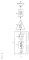
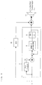
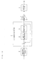
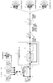
- a ⁇ modulation digital-analogue converter of the present embodiment includes: a ⁇ modulation section ( ⁇ modulation means) 1; a D-Class amplifier (switching amplifier; SW amplifier) 2; an LPF (Low Pass Filter) 3; a nonlinear compensation circuit (compensation means) 6; and a subtractor (subtracting means) 7, as illustrated in Fig. 1 .
- a speaker 11 In the downstream of the low-pass filter 3, a speaker 11 (see Fig. 3 ) is provided.
- the ⁇ modulation section 1 receives a digital signal (original signal) that is encoded from an audio signal of a CD or the like by PCM.
- the ⁇ modulation digital-analogue converter of the present embodiment includes not only a converter dealing with a low electric power (small signal) for almost no load, but also a converter dealing with a large signal for driving a speaker, for example.
- the ⁇ modulation section 1 adds quantization noise generated in the D-Class amplifier to the digital signal, so as to create a binary (or trinary) quantized signal for faithfully amplifying the original signal in the D-Class amplifier 2.
- This ⁇ modulation section 1 includes: a subtractor 8; a group of integrators (integrating means) 4; and a quantizer (quantizing means) 5 provided in the downstream of the group of integrators 4, as illustrated in Fig. 1 .
- the quantized signal outputted from the quantizer 5 is fed back to the subtractor 8 provided in the upstream of the group of integrators 4.
- the subtractor 8 subtracts the quantized signal from the signal received from the upstream of the ⁇ modulation section 1, the quantized signal being created by the quantizer 5. Thereby the subtractor 8 creates a difference signal.
- the group of integrators 4 includes: a plurality of integrators whose transfer function is such that, for example, a plurality of "1/(1-z -1 )" are continuously connected, and/or a plurality of "1/(1-z -1 )" are partially fed back; and multipliers provided between the respective integrators.
- the group of integrators 4 performs integration of the difference signal, and then outputs the integrated difference signal to the quantizer 5.
- the quantizer 5 quantizes, at every predetermined sampling cycle, the output of the group of integrators 4, so as to create a binary ("0" or "1") quantized signal. Then, the quantizer 5 outputs the quantized signal to the D-Class amplifier 2.
- the quantizer 5 of the present embodiment is not limited to the one that creates a binary signal, and may be the one that creates a trinary signal. In a case where the quantizer 5 creates a trinary signal, the arrangement requires more signal lines via which the quantizer 5 and the D-Class amplifier 2 are connected to each other.
- the D-Class amplifier 2 carries out switching in accordance with the quantized signal, so as to switch over constant voltages to each other. This creates a high-voltage switching pulse corresponding to the quantized signal, so that the quantized signal is amplified.
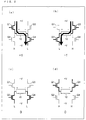
- the D-Class amplifier 2 can be constituted by a full-bridge circuit including four MOSFETs (metal-oxide semiconductor field effect transistor) Q1 through Q4, as illustrated in (a) of Fig. 2 through (d) of Fig. 2 , for example.
- MOSFETs metal-oxide semiconductor field effect transistor
- the MOSFETs Q1 and Q3 are connected to a constant voltage +V, and the MOSFETs Q2 and Q4 are connected to a constant voltage -V. Further, the MOSFETs Q1 and Q2 are provided on a + side with respect to the load 10, and the MOSFETs Q3 and Q4 are provided on a - side with respect to the load 10.
- the constant voltage -V may be set as a ground level.
- an output of the D-Class amplifier 2 is set to be "+1" for a case where the Q1 and Q4 are turned on, and simultaneously the Q2 and Q3 are turned off, and the output of the D-Class amplifier 2 is set to be "-1" for a case where the Q1 and Q4 are turned off, and simultaneously the Q2 and Q3 are turned on.
- the quantizer 5 creates a binary signal
- the low-pass filter 3 smoothes the switching pulse outputted from the D-Class amplifier 2, so as to demodulate the switching pulse. Then, the low-pass filter 3 outputs an analogue signal thus prepared from the original audio signal.
- the subtractor 7 subtracts, from the original signal, the output signal (compensation signal) of the nonlinear compensation circuit 6, so as to create a difference signal.
- the nonlinear compensation circuit 6 is set so as to output a signal whose sign is opposite to that of the signal set by the output signal (compensation signal) of the nonlinear compensation circuit 6, and (ii) an adder (adding means) is used in place of the subtractor (subtracting means) 7.
- the nonlinear compensation circuit (compensation means) 6 includes a look-up table (storage means).
- a look-up table an association table, in which a plurality of original signals, and compensation values are individually associated with each other, is stored, so that the nonlinear compensation circuit 6 can output the compensation values accordingly.
- the following description deals with details of the compensation values stored in the look-up table.
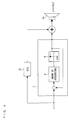
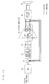
- Fig. 3 is a block diagram illustrating the ⁇ modulation section 1, D-Class amplifier 2, and the low-pass filter 3, which are a part of the ⁇ modulation digital-analogue converter illustrated in Fig. 1 .
- the speaker 11 is illustrated in the downstream of the low-pass filter 3.
- the quantizer 5 is arranged to create a binary signal.
- the arrangement is not limited to this, and the quantizer 5 may be arranged to create a trinary signal.
- the speaker 11 is not particularly limited, and may be either another load, or an electroacoustic transducer which is connected to a plurality of speakers via an electric circuit network (i.e. network) constituted by passive elements (a coil, a capacitor, and a resistance).
- the D-Class amplifier 2 has a nonlinear characteristic. That is, there is a nonlinear relationship between an input toward the D-Class amplifier 2 and an output that the D-Class amplifier 2 outputs with respect to the input. Accordingly, the D-Class amplifier 2 outputs such a signal that distortion is added to the input. This causes a problem that faithful amplification cannot be carried out.
- the distortion is generated due to the nonlinear characteristic of the D-Class amplifier 2.
- the low-pass filter 3 has the nonlinear characteristic (not to an extent of the D-Class amplifier 2 though). This nonlinear characteristic of the low-pass filter 3 also increases the distortion.
- a model diagram (image diagram) of Fig. 4 which is an example of the easiest model of the generation of the distortion.
- a gain from an input to an output is 1.
- Fig. 4 the distortion generated in the output due to the nonlinear characteristic of the D-Class amplifier 2 illustrated in Fig 3 is shown as a block of a distortion generating section (d(x)) 15.
- a distortion factor i.e.
- a nonlinear function that depends on an original signal x (an "input value of an input signal” recited in Claims), which is externally supplied, is added to the output of the quantizer 5.
- the inventors of the present invention found that, as illustrated in Fig. 4 , the distortion generated due to the nonlinear characteristic of the D-Class amplifier 2 depends on the original signal x. If such a nonlinear function d(x) is added to the original signal x, a Fourier transform (frequency analysis) of the output of the ⁇ modulation digital-analogue converter (i.e. an output of the low-pass filter 3) or of the output of the D-Class amplifier 2 generates odd-order harmonics. That is, the inventors of the present invention found that a model in which the odd-order harmonics are generated is the one to which the nonlinear function d(x) depending on a pulse density (depending on the original signal x) is newly added.
- the inventors of the present invention found that if an approximate value of such a nonlinear function d(x) that depends on the original signal x and is generated mainly due to the nonlinear characteristic of the D-Class amplifier 2, is subtracted from the original signal x in advance, that is, the approximate value is subtracted from the original signal x in the upstream of the ⁇ conversion section 1, an influence of the distortion generated in the D-class amplifier 2 is minimized, whereby the original signal x, and the output of the ⁇ modulation digital-analogue converter (or the output of the D-Class amplifier 2) show approximately a linear relationship.
- the inventors of the present invention found a technique of (i) creating a compensation function f(x) by estimating the characteristic of the nonlinear function d(x) of the D-Class amplifier 2 (or the low-pass filter 3), (ii) creating a nonlinear table (look-up table) in which the compensation function f(x) is stored, and (iii) subtracting data stored in the nonlinear table from the original signal x in advance.
- Fig. 5 is a view of such a model that the nonlinear table in which the compensation function f(x) is stored is added to the arrangement illustrated in Fig. 4 .
- a block of a distortion compensation section 16 including the nonlinear table is provided in addition to the model illustrated in Fig. 4 .
- the group of integrators 4 receives such a signal that the compensation function f(x) outputted from the distortion compensation section 16 is subtracted from the original signal x.
- This makes it possible to subtract the compensation function f(x) from the nonlinear function d(x).
- the influence of the distortion generated due to the nonlinear characteristic of the D-Class amplifier 2 can be minimized. Accordingly, it becomes possible to suppress the odd-order harmonics of a power spectrum that is obtained in such a manner that the output of the D-Class amplifier 2 or the output of the ⁇ modulation digital-analogue converter is subjected to the Fourier transform.
- a certain sine wave is inputted as the original signal x.
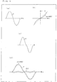
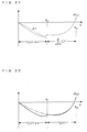
- FIG. 6 is a view showing the nonlinear characteristic of the D-Class amplifier 2 and the low-pass filter 3.
- (d) of Fig. 6 is a view showing waveforms of the output signal y, the original signal x, and the nonlinear function d(x).
- (d) of Fig. 6 shows a nonlinear function d(x) of a third-order harmonic having a frequency three times that of a fundamental harmonic in a case where a waveform measured as the waveform of the original signal x is provided as the fundamental harmonic (first-order harmonic),.
- the output signal y of the D-Class amplifier 2 (or the output signal y of the ⁇ modulation digital-analogue converter) is subjected to the Fourier transform (i.e. the frequency analysis), odd-order harmonics which have frequencies three times, five times, seven times... more than that of the fundamental harmonic, respectively, are generated as the distortion, due to the nonlinear function d(x), as shown in Fig. 7 .
- a frequency spectrum shows large values at frequencies A times (A is an odd number) that of the fundamental harmonic.
- a longitudinal axis indicates a magnitude of the frequency spectrum
- a lateral axis indicates the frequency.
- the odd-order harmonics are generated in the output signal y due to the nonlinear characteristic of the D-class amplifier 2 and the nonlinear characteristic of the low-pass filter 3, that is, the nonlinear function d(x).
- the original signal x and the output signal y become as represented by the following Formula 3.
- a 1 sin( ⁇ t) corresponds to "Gx” of Formula 1
- a 3 sin(3 ⁇ t)+a 5 sin(5 ⁇ )t)+a 7 sin(7 ⁇ t)+ ⁇ corresponds to "f(x)" of Formula 1.
- the amplitude value a s is a magnitude of an amplitude value of the sine wave (fundamental harmonic) of the original signal x that is externally supplied
- the amplitude value a 1 is a magnitude of an amplitude value of a signal having a frequency (which has been actually measured by use of a spectrum analyzer) equal to that of the fundamental harmonic
- the amplitude value a 3 is a magnitude of an amplitude value of a signal having a frequency (which has been also actually measured by use of the spectrum analyzer) three times that of the fundamental harmonic.
- a relationship between the output signal y and the original signal x can show approximately a linear relationship if (i) such a value (compensation value) that the value of the output signal y depends on the original signal x, and the value can cancel a part except "(a 1 / a s )x" on the right side of Formula 6 (i.e. a d(x) component) as much as possible, is determined, and (ii) the value is subtracted from the original signal x.
- the inventors of the present invention found that the d(x) component in Formulas 3 and 6 breaks the linear relationship between the original signal x and the output signal y, and should be cancelled. The following description explains how to determine the compensation value for working out the d(x) component.
- This Formula 7 is such a formula that the d(x) component is merely cancelled in Formula 6. If the output signal y becomes as shown in Formula 7, the relationship between the output signal y and the original signal x will show approximately the linear relationship.
- This Formula 8 can be obtained from Formula 7 by replacing the d(x) component in Formula 6 with "+d(x)-d(x)".
- Formula 8 is converted into the following Formula 9.
- y ⁇ a 1 a s x ⁇ a s a 3 a 1 sin 3 sin ⁇ 1 x a s ⁇ a s a 5 a 1 sin 5 sin ⁇ 1 x a s ⁇ a s a 7 a 1 sin 7 sin ⁇ 1 x a s ⁇ ⁇ + a 3 sin 3 sin ⁇ 1 x a s + a 5 sin 5 sin ⁇ 1 x a s + a 7 sin 7 sin ⁇ 1 x a s + ⁇
- the original signal x is compensated into the x', and an output of the x' is checked.
- the output signal y' which is the output signal y in which the d(x) component is cancelled as much as possible.
- f x a s a 3 a 1 sin 3 sin ⁇ 1 x a s + a s a 5 a 1 sin 5 sin ⁇ 1 x a s + a s a 7 a 1 sin 7 sin ⁇ 1 x a s + ⁇
- the following description specifically explains a procedure of determining a value of the compensation function f(x) by referring to the correspondence relationship between the original signal x and the compensation function f(x), which value will be stored in the look-up table.
- the output of the nonlinear compensation circuit 6 is set to be 0, and the sine wave having the amplitude value a s is supplied as the original signal x.
- a dB value of the amplitude value a s is A s .
- the fundamental harmonic, and the odd-order harmonics (the third-order harmonic, the fifth-order harmonic%) belong to, that is, (1) a state where a phase of the fundamental harmonic, and phases of the odd-order harmonics (the third-order harmonic, the fifth-order harmonic%) have in-phase components, (2) a state where the phase of the fundamental harmonic, and the phases of the odd-order harmonics (the third-order harmonic, the fifth-order harmonic%) have out-of-phase components, or (3) a state where the phase of the fundamental harmonic, and the phases of the odd-order harmonics (the third-order harmonic, the fifth-order harmonic...) have neither the in-phase components nor the out-of-phase components.
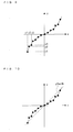
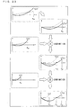
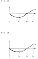
- the state where the phase of the fundamental harmonic, and the phases of the odd-order harmonics (the third-order harmonic, the fifth-order harmonic%) have in-phase components means a case where the nonlinear characteristic of the D-Class amplifier 2 and of the low-pass filter 3 is shown in an S-shaped curve, as shown in (b) of Fig. 8 .
- the original signal x and the nonlinear function d(x) are substantially in phase.
- the state where the phase of the fundamental harmonic, and the phases of the odd-order harmonics (the third-order harmonic, the fifth-order harmonic%) have out-of-phase components means a case where the nonlinear characteristic of the D-Class amplifier 2 and of the low-pass filter 3 is shown in a reversed S-shaped curve, as shown in (d) of Fig. 8 .
- the original signal x and the nonlinear function f(x) are substantially in phase.
- the state where the phase of the fundamental harmonic, and the phases of the odd-order harmonics (the third-order harmonic, the fifth-order harmonic%) have neither the in-phase components nor the out-of-phase components means a case where the nonlinear characteristic of the D-Class amplifier 2 and of the low-pass filter 3 is shown in a hysteresis loop shape, as shown in (f) of Fig. 8 .
- the original signal x and the nonlinear function f(x) are neither in phase nor out of phase.
- the relationships between the phase of the fundamental harmonic, and the phases of the odd-order harmonics are actually examined.
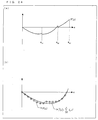
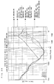
- Fig. 11 is a view of a waveform, showing that the odd-order harmonics were actually suppressed with the use of the nonlinear compensation circuit 6 of the present embodiment. More specifically, Fig. 11 shows a frequency spectrum which can be obtained in such a manner that the output signal of the ⁇ modulation digital-analogue converter or the output signal of the D-Class amplifier 2 is subjected to the frequency analysis. The spectrum in the vicinity of 1kHz shows a signal component of an amplified fundamental harmonic (sine wave). By comparing Fig. 11 with the aforementioned Fig. 15 , it can be clearly seen that the odd-order harmonics are suppressed.
- the odd-order harmonics are generated due to the nonlinear characteristic of both the D-Class amplifier 2 and the low-pass filter 3. Since the odd-order harmonics are mainly generated due to the nonlinear characteristic of the D-Class amplifier 2, it is possible to set the compensation value to suppress only the odd-order harmonics generated due to the nonlinear characteristic of the D-class amplifier 2. Alternatively, it is also possible to set the compensation value to suppress the odd-order harmonics generated due to the nonlinear characteristic of both the D-Class amplifier 2 and the low-pass filter 3.
- the output of the D-Class amplifier 2 is subjected to the frequency analysis, it becomes possible to suppress the odd-order harmonics generated due to only the nonlinear characteristic of the D-Class amplifier 2.
- the output of the low-pass filter 3 that is, the output of the ⁇ modulation digital-analogue converter, is subjected to the frequency analysis, it becomes possible to suppress the odd-order harmonics generated due to the nonlinear characteristic of both the D-Class amplifier 2 and the low-pass filter 3.
- the method of working out the compensation function f(x), that is, the compensation value is not limited to the aforementioned first method, and the compensation value may be worked out by the following method.
- the output of the nonlinear compensation circuit 6 is set to be 0. Then, as shown in Fig. 9 , a plurality of output signals y(t) of the D-Class amplifier 2 (or the ⁇ modulation digital-analogue converter) are measured at the time an original signal x(t) is inputted at a certain time t, so that a plurality of combinations of the x(t) and y(t) (i.e. a plurality of x-y coordinates) are determined.
- the N may be any integer as long as the integer is not less than 3.
- the reason why it is necessary to measure not less than 3 coordinates is that a measurement of two coordinates provides only information of a straight line. Such information does not include the information that can be used for the compensation (information of a difference between the output y and the straight line).
- f(x i ) which is an error between the straight line shown by the above Formula 14 and an actual input-output curve that is formed in such a manner that the coordinates measured as described above are connected to each other.
- f x i y i ⁇ ax i + b
- This f(x i ) may be stored in the look-up table described above as the compensation function, that is, the compensation value.
- An object of the method is, as described above, to suppress the harmonics by linearizing the relationship between the input and output of the ⁇ modulation (that is, to cause the output y of the ⁇ modulation to be close to the equation of the straight line of "ax+b").
- the x i and y i are data of a result of "distortion" due to a digital amplifier. Further, the following description deals with a proof that the linear characteristic can be realized by this method.
- the compensation functions have been determined by experiments, and stored in the look-up table in advance. That is, the look-up table has been provided in the nonlinear compensation circuit 6.
- the present invention is not limited to the arrangement, and the nonlinear compensation circuit 6 may be provided with the following calculation circuit (calculation means).
- the calculation circuit is arranged to (i) receive an output signal from the D-Class amplifier 2 or the ⁇ modulation digital-analogue converter, (ii) compare the output signal with an original signal, and (iii) calculate out a compensation function (compensation value) for each output signal.
- the subtractor 7 is provided on a route from an end to which the original signal x is inputted to the ⁇ modulation section 1, and a difference signal, which has been obtained in such a manner that the output signal of the nonlinear compensation circuit 6 is subtracted from the original signal, is inputted into the ⁇ modulation section 1.
- the present invention is not limited to the arrangement.
- the ⁇ modulation digital-analogue converter of the present embodiment may be arranged such that the subtractor 7 is removed from the arrangement illustrated in Fig. 1 , and the nonlinear compensation circuit 6 is provided on the route from the end to which the original signal x is inputted to the ⁇ modulation section 1.
- the nonlinear compensation circuit 6 is arranged to include a look-up table that outputs x-f(x) with respect to the input x.
- the nonlinear compensation circuit 6 is arranged to include a look-up table that outputs x i -d(x i ) with respect to the input x.
- a ⁇ modulation digital-analogue converter for converting a quantized signal received from ⁇ modulation means into an analogue signal includes: a nonlinear compensation circuit for outputting a compensation signal in accordance with a supplied input signal; adding means for adding the compensation signal to the supplied input signal; and the ⁇ modulation means for modulating an output of the adding means into the quantized signal; wherein an output value of the nonlinear compensation circuit is calculated out from a harmonic distortion component of a power spectrum of an output of the ⁇ modulation digital-analogue converter, the harmonic distortion component being obtained in a case where (i) a sine wave having a single frequency is supplied to an input of the ⁇ modulation digital-analogue converter, and (ii) the output of the nonlinear compensation circuit is set to be 0.
- the nonlinear compensation circuit may determine a compensation value in such a manner that (i) a value of an output y is measured when an input x is supplied, and (ii) the compensation value is determined from a correspondence relationship between the input x and the output y.
- the present invention includes a nonlinear compensation circuit, an adder, a ⁇ modulator, an SW amplifier, and a low-pass filter, and in order to calculate a value of a compensation table, (i) the value of the compensation table is set to be 0, (ii) a power spectrum of a corresponding AD output is obtained when a sine wave having a single frequency is inputted into a corresponding DA, (iii) an output having a frequency equal to that of the inputted sine wave is determined as a fundamental harmonic, and (iv) an amplitude value of the fundamental harmonic and amplitude values of odd-order harmonics of the fundamental harmonic are measured. From a result of the measurement, the compensation table is created based on calculation formulas.
- the compensation value is determined in such a manner that (i) the value of the output y is measured when the input x is supplied, (ii) the correspondence relationship between the output y and the input x is calculated out by the least square method, and (iii) the compensation value is determined from the result of the calculation. Then, if the DA conversion is carried out by use of the compensation table, the odd-order harmonics are suppressed.
- advantages of the present invention may be expressed such that the effect of the present invention includes advantages as follows: (a) it is possible to improve an SNR and a THD+N, as compared with a ⁇ modulation analogue-digital converter employing a full open loop technique; (b) it is possible to reduce costs with a simple circuit arrangement in which an analogue feedback circuit is not provided to carry out a feedback from the SW amplifier; (c) since a nonlinear table is determined from harmonics measured based on the Fourier transform, it is possible to create a high-accuracy compensation table which is hardly affected by an accidental error in a measurement system; (d) the present invention can be applied to various SW amplifiers only by rewriting the compensation table; (e) as to the odd-order harmonics, if the odd-order harmonics and the input signal have either in-phase components, or out-of-phase components, it is possible to suppress a component higher than a third-order harmonic component; and (f) it is possible to contribute to power conservation by suppressing
- the input signal is a sine wave.
- the input signal is not limited to a sine wave, but may be a triangular wave, a rectangular wave, or the like.
- First Embodiment corresponds to a first compensation function recited in Claims.
- the description is made for a case where one compensation value is provided for one ⁇ modulation digital-analogue converter.
- the present invention is not limited to this, and a plurality of compensation values may be prepared in one ⁇ modulation digital-analogue converter in advance.
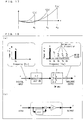
- a ⁇ modulation digital-analogue converter of the present embodiment includes: a compensation value memory (for 4 ⁇ ) 31 suitable for a 4 ⁇ speaker 36; a compensation value memory (for 6 ⁇ ) 32 suitable for a 6 ⁇ speaker 37; a compensation value memory (for 8 ⁇ ) 33 suitable for a 8 ⁇ speaker 38; a compensation value (for a general purpose) 34 for a general-purpose speaker (not illustrated); and a selector switch 35, as illustrated in Fig. 16 .
- a compensation value stored in the compensation value memory (for 4 ⁇ ) 31 is inputted into the nonlinear compensation circuit 6.
- a compensation value stored in the compensation value memory (for 6 ⁇ ) 32 (or the compensation value memory (for 8 ⁇ ) 33) is inputted into the nonlinear compensation circuit 6.
- the compensation value memory (for 4 ⁇ ) 31, the compensation value memory (for 6 ⁇ ) 32, the compensation value memory (for 8 ⁇ ) 33, and the compensation value memory (for a general purpose) 34 are provided separately from the nonlinear compensation circuit 6.
- nonlinear compensation circuits for 4 ⁇ , 6 ⁇ , 8 ⁇ , and a nonlinear compensation circuit for a general purpose may be provided for the compensation value memories respectively.
- the compensation value memory "for a general purpose” may be a memory to which a compensation value that is most suitable for a speaker is written via a microcomputer in a case where a speaker having an impedance other than impedances of 4 ⁇ , 6 ⁇ , and 8 ⁇ is provided. Furthermore, the compensation value memory "for a general purpose” may be a memory in which a common compensation value is stored for a speaker having an impedance of not less than 10 ⁇ , for example.
- the compensation value and the compensation function are determined without taking into consideration a magnitude of an amplitude value of the original signal.
- the compensation value and compensation function that are most suitable for a certain amplitude value are not always most suitable for another amplitude value.
- a compensation function that is most suitable for an amplitude value a s1 is f 1 (x)
- a compensation function that is most suitable for an amplitude value a s2 is f 2 (x)
- a compensation function that is most suitable for an amplitude value a s3 is f 3 (x)
- (1) f 2 (x) and f 3 (x) are not most suitable for the amplitude value a s1
- (2) f 1 (x) and f 3 (x) are not most suitable for the amplitude value a s2
- (3) f 1 (x) and f 2 (x) are not most suitable for the amplitude value a s3 (see Fig. 17 ).
- the switching amplifier (D-Class amplifier) 2 outputs the harmonics having the amplitude values a 1 , a 3 , a 5 , a 7 and a 9 , respectively.
- (b) of Fig. 18 is a schematic view of an arrangement from the input to the output, in consideration of the ⁇ modulation section 1, the switching amplifier 2, and distortion components.
- the nonlinear compensation circuit 6 is provided so as to compensate the input signal in the upstream of the ⁇ modulation section 1. That is, as illustrated in Fig. 19 , the harmonics are suppressed by adding a first compensation function f(x) to the input x.
- a first compensation function f(x) to the input x.
- an output y' can be expressed by the following formula.
- y ⁇ G x + f x + d x + f x where
- an ideal output y' having no harmonics is expressed by the following formula.
- y ⁇ Gx
- Gx G x + f x + d x + f x
- x x + f x + d x + f x
- f x ⁇ d x + f x That is, f(x) can be expressed by the following formula.
- the compensation function for each amplitude value corresponds to a second compensation function recited in Claims.
- the compensation function f(x) can be determined from a parameter including: the amplitude a s (which is known data) of the input; the output fundamental harmonic a 1 (which is measurable data); and the harmonic a n (which is measurable data).
- the compensation function f(x) is realized by polynomial representation of the following formula employing a factor c m .
- the factor "c m " is represented by conversion of a matrix employing a s , a 1 , and an, so that it is possible to represent Formulas A and B. A proof of this will be described later.
- the following description deals with an example of working out the compensation function.
- the description deals with a case where the compensation is carried out up to the third-order harmonic.
- the polynomial representation that allows the compensations up to the third-order harmonic can be represented by the following Formula 22.
- f x c 1 x + c 3 x 3
- Formula 23 By substituting Formula 18 in Formula 22, the following Formula 23 can be obtained.
- f x c 1 a s sin ⁇ t + c 3 a s sin ⁇ t 3
- a factor of c 1 appears with respect to the fundamental harmonic component. This is because the c 1 absorbs a change, due to an influence of the nonlinear compensation, in the gain G, so as to play a role of keeping the gain G to be constant (keeping a previous gain G and a following gain G to be the same).
- Formula 25 is converted into the following Formula 27.
- the following description explains a method of determining, in a case of a single amplitude, (i) a compensation function that compensates the harmonics not less than the third-order harmonic, and (ii) a factor of the compensation function. That is, the following description deals with a case where the compensation is carried out with respect to up to the n-order harmonic.
- Formula 40 By substituting Formula 33 in Formula 39, the following Formula 40 can be obtained.
- Formula 43 can be represented by the following Formula 44.
- a variable a n ' is newly defined as described below.
- a 1 ⁇ 0
- a n ⁇ a s a n / a 1
- Formulas 46 and 47 are converted into the following Formula 48.
- Formula 48 is converted into Formula 50.
- Formula 57 can be obtained.
- ⁇ a 1 ⁇ a 3 ⁇ a 5 ⁇ ⁇ a N ⁇ q 1 q 3 q 5 ⁇ q N b 1 1 0 0 0 b 3 1 b 3 3 0 0 b 5 1 b 5 3 b 5 5 0 ⁇ ⁇ ⁇ ⁇ b N 1 b N 3 b N 5 b N N
- Formula 59 can be represented by the following formula.
- ⁇ a cSB If "c” is obtained by modifying the formula of the matrix, the following formula can be obtained.
- c ⁇ a SB ⁇ 1 Therefore, c m can be determined by use of a calculator.
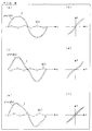
- f 1 (x) and f 2 (x) are as shown in Fig. 20 .
- curves of the f 1 (x) and f 2 (x) which have been determined from two different amplitude values, generally do not overlap each other, in practice. Accordingly, for appropriate combination of these functions, the point is how appropriately f 1 (x) is combined with f 2 (x) while reflecting the curve of f 2 (x).
- a function (graph) of f 1 (x) can be tilted by a minute number " ⁇ " compared with a s1 .
- the gain in an interval of [0:a s1 ] changes to a certain degree, but the change does not cause any problems.
- f 1 (x) is tilted by a minute number ⁇ so as to be close to the curve of f 2 (x) as much as possible.
- an optimum combined function f*(x) is considered as such a function that (i) f 1 (x) is tilted by ⁇ so that a gradient of f 1 (x) becomes the same as a gradient of f 2 (x) in the interval of [0:a s1 ], and (ii) the two functions of f 1 (x) and f 2 (x) are combined (synthesized) with each other at the point a s1 .
- This method for combining two functions can be also applied to a case where not less than three graphs are provided (see Fig. 23 ). That is, combination of a compensation function corresponding to a second-largest amplitude value and a compensation function corresponding to a largest amplitude value is carried out such that the compensation function corresponding to the second-largest amplitude value is tilted in accordance with the compensation function corresponding to the largest amplitude value. Further, combination of the combined compensation function and a compensation function corresponding to a third-largest amplitude value is carried out in the same manner as described above. By continuing to carry out such combination in the same manner, one combined function is created.
- the curve fitting can be carried out by use of the following Formula 62.
- intervals between samples used in an approximation of the curve fitting may be, as shown in Fig. 25 , provided equally.
- the intervals may have high density in the vicinity of a small amplitude region that has a great influence on a performance of a valley of a THD, so that precision of the approximation during a small amplitude period can be improved.
- the over-fitting means that an excess increase in the number of parameters causes the fitting curve to be sensitive to an accidental error of mathematical calculation, so that the fitting curve has an unnatural waveform.
- the present embodiment achieves the following advantages. For example, among a case (a) where the compensation is not carried out, a case (b) where the compensation is carried out in accordance with an amplitude value of -8dB, a case (c) where the compensation is carried out in accordance with amplitude value of -3dB, and a case (d) where the compensation is carried out in accordance with amplitude values -8dB and -3dB, if curves of a ratio of the output to distortion are compared with each other, the distortion is suppressed in a widest range in the case (d) where the compensation is carried out in accordance with the amplitude values of -8dB and -3dB (see Fig. 27 ).
- the present inventions are common in that the distortion is generated depending on the input x. However, with the present invention, not a unique model but a plurality of models are used for the model of the generation of the distortion. An adequacy or appropriateness of the model is determined depending on whether or not the distortion is cancelled when the method of reducing the distortion by using the model is worked out and applied. The present invention explains three kinds of model among various models of the generation of the distortion.
- the first model is most suitable for easy explanation of the principle of realizing suppression of the distortion.
- any of the ⁇ modulation digital-analogue converters described above can be applied to AV equipment (AV device) such as audio equipment or a television.
- a ⁇ modulation digital-analogue converter of the present invention includes: ⁇ modulation means including integrating means including at least one integrator for integrating a digital signal, and quantizing means for modulating an output of the integrating means into a quantized signal, the ⁇ modulation means feeding back the quantized signal to an upstream of the integrating means; a switching amplifier for generating a switching pulse in accordance with the quantized signal; a low-pass filter for demodulating the switching pulse; storage means in which a first compensation function is stored in advance, the first compensation function indicating a correspondence relationship between each of a plurality of possible input values of an input signal which is externally supplied, and each of compensation values that are individually associated with the possible input values; and compensation means for compensating the input signal which is externally supplied, based on a compensation value associated with the input signal among the compensation values, and supplying to the ⁇ modulation means the input signal thus compensated; the first compensation function being set based on a spectrum of odd-order harmonics whose frequencies are A times
- a ⁇ modulation digital-analogue converter of the present invention includes: ⁇ modulation means including integrating means including at least one integrator for integrating a digital signal, and quantizing means for modulating an output of the integrating means into a quantized signal, the ⁇ modulation means feeding back the quantized signal to an upstream of the integrating means; a switching amplifier for generating a switching pulse in accordance with the quantized signal; a low-pass filter for demodulating the switching pulse; calculating means for calculating, in accordance with an output of the switching amplifier or an output of the ⁇ modulation digital-analogue converter, each of compensation values that compensate individually a plurality of possible input values of an input signal which is externally supplied; and compensation means for compensating the input signal which is externally supplied, based on a compensation value associated with the input signal among the compensation values, and supplying to the ⁇ modulation means the input signal thus compensated, the calculating means working out the compensation value based on magnitudes of a spectrum of odd-order harmonics whose frequencies are
- a digital signal processing method of the present invention employs a ⁇ modulation digital-analogue converter
- the ⁇ modulation digital-analogue converter including: ⁇ modulation means including integrating means including at least one integrator for integrating a digital signal, and quantizing means for modulating an output of the integrating means into a quantized signal, the ⁇ modulation means feeding back the quantized signal to an upstream of the integrating means; a switching amplifier for generating a switching pulse in accordance with the quantized signal; a low-pass filter for demodulating the switching pulse, the method including: providing, to the ⁇ modulation digital-analogue converter, storage means in which a first compensation function is stored in advance, the first compensation function indicating a correspondence relationship between each of a plurality of possible input values of an input signal which is externally supplied, and each of compensation values that are individually associated with the possible input values; and providing compensation means to the ⁇ modulation digital-analogue converter and compensating, by the compensation means, the input signal which is externally
- a ⁇ modulation digital-analogue converter of the present invention is applicable to audio equipment, a television, or the like.
Landscapes
- Engineering & Computer Science (AREA)
- Power Engineering (AREA)
- Physics & Mathematics (AREA)
- Nonlinear Science (AREA)
- Theoretical Computer Science (AREA)
- Amplifiers (AREA)
- Analogue/Digital Conversion (AREA)
- Amplitude Modulation (AREA)
Claims (15)
- Δ∑-Modulations-Digital-Analog-Wandler, aufweisend:Kompensationsmittel (6) zum Kompensieren eines Eingangssignals basierend auf einem Kompensationswert, der mit dem Eingangssignal verknüpft ist, unter den Kompensationswerten, um ein digitales Signal zu erzeugen;Δ∑-Modulations-Mittel (1), das ein integrierendes Mittel (4) enthält, welches zumindest einen Integrator zum Integrieren des vom Kompensationsmittel (6) gelieferten digitalen Signals enthält, und ein quantisierendes Mittel (5) zum Modulieren einer Ausgabe des integrierenden Mittels (4) in ein quantisiertes Signal, wobei das Δ∑-Modulations-Mittel (1) das quantisierte Signal vorgelagert zum integrierenden Mittel (4) rückkoppelt;einen Schaltverstärker (2) zum Erzeugen eines Schaltimpulses gemäß dem quantisierten Signal;einen Tiefpassfilter (3) zum Demodulieren des Schaltimpulses; undSpeichermittel, worin eine erste Kompensationsfunktion vorab gespeichert wird, wobei die erste Kompensationsfunktion eine Korrespondenzbeziehung zwischen jedem einer Mehrzahl möglicher Eingabewerte des Eingangssignals und jedem der Kompensationswerte angibt, die mit den möglichen Eingabewerten individuell verknüpft sind;dadurch gekennzeichnet, dassdie erste Kompensationsfunktion basierend auf einem Spektrum von Oberschwingungen nur ungerader Ordnungen eingerichtet ist, deren Frequenzen A-mal höher als eine Frequenz des Eingangssignals sind (A ist eine ungerade Zahl), wobei das Spektrum durch eine Frequenzanalyse des Schaltimpulses oder einer Ausgabe des Tiefpassfilters erhalten wird, wobei das Eingangssignal direkt in das Δ∑-Modulations-Mittel als das digitale Signal eingespeist wird.
- ∑Δ-Modulations-Digital-Analog-Wandler nach Anspruch 1, wobei:die erste Kompensationsfunktion erhalten wird, indem zweite Kompensationsfunktionen kombiniert werden, welche jeweils für verschiedene Amplitudenwerte des Eingangssignals stehen und jeweils Korrespondenzbeziehungen zwischen den möglichen Eingabewerten und den Kompensationswerten für die verschiedenen Amplitudenwerte angeben.
- Δ∑-Modulations-Digital-Analog-Wandler nach Anspruch 1, wobei:die erste Kompensationsfunktion auf solch eine Weise erhalten wird, dass (i) zweite Kompensationsfunktionen, welche jeweils für verschiedene Amplitudenwerte des Eingangssignals stehen und jeweils Korrespondenzbeziehungen zwischen den möglichen Eingabewerten und den Kompensationswerten für die verschiedenen Amplitudenwerte angeben, kombiniert werden und (ii) eine resultierende kombinierte Funktion einer Kurvenanpassung unterzogen wird.
- ∑Δ-Modulations-Digital-Analog-Wandler nach Anspruch 2, wobei:die zweiten Funktionen auf solch eine Weise kombiniert werden, dass eine Kombination einer zweiten Funktion entsprechend einem höchsten Amplitudenwert und einer zweiten Funktion entsprechend einem zweithöchsten Amplitudenwert eine nach der anderen sequentiell ausgeführt wird.
- Δ∑-Modulations-Digital-Analog-Wandler nach Anspruch 1, wobei:die erste Kompensationsfunktion im Speichermittel pro Impedanz einer Last gespeichert wird.
- Δ∑-Modulations-Digital-Analog-Wandler nach Anspruch 5, wobei:die Last ein Lautsprecher (36,37, 38) ist.
- Δ∑-Modulations-Digital-Analog-Wandler nach Anspruch 5, wobei:die Last ein elektrisches Schaltnetzwerk ist, mit welchem eine Mehrzahl von Lautsprechern (36, 37, 38) verbunden ist.
- ∑Δ-Modulations-Digital-Analog-Wandler nach Anspruch 1, ferner aufweisend:subtrahierendes Mittel zum (i) Erzeugen eines Differenzsignals, indem der Kompensationswert vom Eingangssignal subtrahiert wird, und (ii) Einspeisen des Differenzsignals als das Eingangssignal in das Δ∑-Modulations-Mittel.
- Δ∑-Modulations-Digital-Analog-Wandler nach Anspruch 1, ferner aufweisend:addierendes Mittel zum (i) Erzeugen eines Summensignals, indem der Kompensationswert zum Eingangssignal addiert wird, und (ii) Einspeisen des Summensignals als das Eingangssignal in das Δ∑-Modulations-Mittel.
- Δ∑-Modulations-Digital-Analog-Wandler nach Anspruch 1, wobei:die Amplitudenwerte von Oberschwingungen, die gleich oder höher als eine Oberschwingung dritter Ordnung sind, so bestimmt werden, dass, (i) falls die Oberschwingungen und eine Oberschwingung erster Ordnung phasengleiche Komponenten aufweisen, Vorzeichen der Amplitudenwerte positiv sind und, (ii) falls die Oberschwingungen und die Oberschwingung erster Ordnung phasenverschobene Komponenten aufweisen, die Vorzeichen der Amplitudenwerte negativ sind.
- Δ∑-Modulations-Digital-Analog-Wandler nach Anspruch 1, wobei:der Kompensationswert yi - (axi + b) ist,
WO:das Eingangssignal an das Δ∑-Modulations-Mittel (1) als das digitale Signal geliefert wird; unda und b nach der Methode der kleinsten Quadrate aus einem Eingabewert xi (i = 1, 2 ..., N; N ist eine ganze Zahl größer 2) des Eingangssignals und einem Ausgabewert yi (i = 1, 2 , ... N; N ist eine ganze Zahl größer 2) eines Ausgangssignals erarbeitet werden, so dass E = ∑i=1 N {(axi + b) - yi}2 deren Minimum wird. - Δ∑-Modulations-Digital-Analog-Wandler nach Anspruch 1, wobei:der Kompensationswert (1+a)xi - yi +b) ist,
WO:das Eingangssignal an das Δ∑-Modulations-Mittel (1) als das digitale Signal geliefert wird; unda und b nach der Methode der kleinsten Quadrate aus einem Eingabewert xi (i = 1, 2 ..., N; N ist eine ganze Zahl größer 2) des Eingangssignals und einem Ausgabewert yi (i = 1, 2 , ... N; N ist eine ganze Zahl größer 2) eines Ausgangssignals berechnet werden, so dass E = Σi=1 N {(axi + b) - yi}2 deren Minimum wird. - Δ∑-Modulations-Digital-Analog-Wandler, aufweisend:Kompensationsmittel (6) zum Kompensieren eines Eingangssignals basierend auf einem Kompensationswert, der mit dem Eingangssignal verknüpft ist, unter den Kompensationswerten, um ein digitales Signal zu erzeugen; Δ∑-Modulations-Mittel (1), das ein integrierendes Mittel (4) enthält, welches zumindest einen Integrator zum Integrieren des vom Kompensationsmittel (6) gelieferten digitalen Signals enthält, und ein quantisierendes Mittel (5) zum Modulieren einer Ausgabe des integrierenden Mittels (4) in ein quantisiertes Signal, wobei das Δ∑-Modulations-Mittel (1) das quantisierte Signal vorgelagert zum integrierenden Mittel (4) rückkoppelt;einen Schaltverstärker (2) zum Erzeugen eines Schaltimpulses gemäß dem quantisierten Signal;einen Tiefpassfilter (3) zum Demodulieren des Schaltimpulses; undberechnende Mittel zum Berechnen, gemäß einer Ausgabe des Schaltverstärkers oder einer Ausgabe des Δ∑-Modulations-Digital-Analog-Wandlers, jedes der Kompensationswerte, die eine Mehrzahl möglicher Eingabewerte des Eingangssignals individuell kompensieren;dadurch gekennzeichnet, dassdie berechnenden Mittel dafür eingerichtet sind, den Kompensationswert basierend auf Größen eines Spektrums von Oberschwingungen nur ungerader Ordnungen zu erarbeiten, deren Frequenzen A-mal höher als eine Frequenz des Eingangssignals sind (A ist eine ungerade Zahl), wobei das Spektrum durch eine Frequenzanalyse des Schaltimpulses oder einer Ausgabe des Tiefpassfilters erhalten wird, wobei das Eingangssignal direkt in das Δ∑-Modulations-Mittel als das digitale Signal eingespeist wird.
- AV-Vorrichtung, mit einem Δ∑-Modulations-Digital-Analog-Wandler nach Anspruch 1.
- Digitalsignalverarbeitungsverfahren, welches einen Δ∑-Modulations-Digital-Analog-Wandler verwendet,
wobei der Δ∑-Modulations-Digital-Analog-Wandler enthält:Δ∑-Modulations-Mittel (1), das ein integrierendes Mittel (4) enthält, welches zumindest einen Integrator zum Integrieren eines digitalen Signals enthält, und ein quantisierendes Mittel zum Modulieren einer Ausgabe des integrierenden Mittels (4) in ein quantisiertes Signal, wobei das Δ∑-Modulations-Mittel (1) das quantisierte Signal vorgelagert zum integrierenden Mittel (4) rückkoppelt;einen Schaltverstärker (2) zum Erzeugen eines Schaltimpulses gemäß dem quantisierten Signal;einen Tiefpassfilter (3) zum Demodulieren des Schaltimpulses;wobei der Verfahren aufweist:Vorsehen, zu dem ∑Δ-Modulations-Digital-Analog-Wandler, von Speichermittel, worin eine erste Kompensationsfunktion vorab gespeichert wird, wobei die erste Kompensationsfunktion eine Korrespondenzbeziehung zwischen jedem einer Mehrzahl möglicher Eingabewerte eines Eingangssignals und jedem von Kompensationswerten angibt, die mit den möglichen Eingabewerten individuell verknüpft sind; undVorsehen von Kompensationsmittel (6) zu dem Δ∑-Modulations-Digital-Analog-Wandler und Kompensieren, durch das Kompensationsmittel, des Eingangssignals, basierend auf einem Kompensationswert, der mit dem Eingangssignal verknüpft ist, unter den Kompensationswerten, um das digitales Signal zu erzeugen, und Liefern, durch das Kompensationsmittel, des digitalen Signals an das Δ∑-Modulations-Mittel (1),dadurch gekennzeichnet, dassdie erste Kompensationsfunktion basierend auf einem Spektrum von Oberschwingungen nur ungerader Ordnungen eingerichtet ist, deren Frequenzen A-mal höher als eine Frequenz des Eingangssignals sind (A ist eine ungerade Zahl), wobei das Spektrum durch eine Frequenzanalyse des Schaltimpulses oder einer Ausgabe des Tiefpassfilters erhalten wird, wobei das Eingangssignal direkt in das Δ∑-Modulations-Mittel als das digitale Signal eingespeist wird.
Applications Claiming Priority (2)
| Application Number | Priority Date | Filing Date | Title |
|---|---|---|---|
| JP2006353292 | 2006-12-27 | ||
| PCT/JP2007/075161 WO2008081887A1 (ja) | 2006-12-27 | 2007-12-27 | Δς変調型デジタルアナログ変換器、デジタル信号処理方法、およびav装置 |
Publications (3)
| Publication Number | Publication Date |
|---|---|
| EP2117117A1 EP2117117A1 (de) | 2009-11-11 |
| EP2117117A4 EP2117117A4 (de) | 2012-04-25 |
| EP2117117B1 true EP2117117B1 (de) | 2016-08-10 |
Family
ID=39588568
Family Applications (1)
| Application Number | Title | Priority Date | Filing Date |
|---|---|---|---|
| EP07860383.4A Not-in-force EP2117117B1 (de) | 2006-12-27 | 2007-12-27 | Modulations-digital-analog-umsetzer, digitales signalverarbeitungsverfahren und av-einrichtung |
Country Status (5)
| Country | Link |
|---|---|
| US (1) | US7889109B2 (de) |
| EP (1) | EP2117117B1 (de) |
| JP (1) | JP5143748B2 (de) |
| CN (1) | CN101611543B (de) |
| WO (1) | WO2008081887A1 (de) |
Families Citing this family (28)
| Publication number | Priority date | Publication date | Assignee | Title |
|---|---|---|---|---|
| WO2007135928A1 (ja) | 2006-05-21 | 2007-11-29 | Trigence Semiconductor, Inc. | デジタルアナログ変換装置 |
| JP5552620B2 (ja) | 2008-06-16 | 2014-07-16 | 株式会社 Trigence Semiconductor | デジタルスピーカー駆動装置と集中制御装置とを搭載した自動車 |
| JP5356952B2 (ja) | 2009-08-31 | 2013-12-04 | レムセン イノベーション、リミティッド ライアビリティー カンパニー | 表示装置 |
| JP5231359B2 (ja) * | 2009-08-31 | 2013-07-10 | シャープ株式会社 | デジタルアンプ、daコンバータ、増幅方法、及び、変換方法 |
| JP5271233B2 (ja) * | 2009-10-22 | 2013-08-21 | Kddi株式会社 | 電力増幅器に対応付けてδς変換器の制御値を制御する送信機、プログラム及び方法 |
| JP5568752B2 (ja) | 2009-12-09 | 2014-08-13 | 株式会社 Trigence Semiconductor | 選択装置 |
| CN103096217B (zh) * | 2009-12-16 | 2016-09-28 | 株式会社特瑞君思半导体 | 音响系统 |
| JP2012015650A (ja) * | 2010-06-29 | 2012-01-19 | Renesas Electronics Corp | D級増幅器 |
| JP2012253944A (ja) * | 2011-06-03 | 2012-12-20 | Advantest Corp | ワイヤレス給電装置およびワイヤレス給電システム |
| JP5870308B2 (ja) | 2011-09-20 | 2016-02-24 | パナソニックIpマネジメント株式会社 | Da変換装置及び音声システム |
| RU2488217C2 (ru) * | 2011-10-13 | 2013-07-20 | Федеральное государственное военное образовательное учреждение высшего профессионального образования "Военный авиационный инженерный университет" (г. Воронеж) Министерства обороны Российской Федерации | Способ амплитудной модуляции и демодуляции высокочастотных сигналов и устройство его реализации |
| RU2488945C2 (ru) * | 2011-10-21 | 2013-07-27 | Федеральное государственное военное образовательное учреждение высшего профессионального образования "Военный авиационный инженерный университет" (г. Воронеж) Министерства обороны Российской Федерации | Способ амплитудной, фазовой и частотной модуляции высокочастотных сигналов и многофункциональное устройство его реализации |
| RU2488943C2 (ru) * | 2011-10-21 | 2013-07-27 | Федеральное государственное военное образовательное учреждение высшего профессионального образования "Военный авиационный инженерный университет" (г. Воронеж) Министерства обороны Российской Федерации | Способ амплитудной, фазовой и частотной модуляции высокочастотных сигналов и многофункциональное устройство его реализации |
| RU2488944C2 (ru) * | 2011-10-21 | 2013-07-27 | Федеральное государственное военное образовательное учреждение высшего профессионального образования "Военный авиационный инженерный университет" (г. Воронеж) Министерства обороны Российской Федерации | Способ амплитудной, фазовой и частотной модуляции высокочастотных сигналов и многофункциональное устройство его реализации |
| US9136865B2 (en) * | 2014-02-11 | 2015-09-15 | Taiwan Semiconductor Manufacturing Company, Ltd. | Multi-stage digital-to-analog converter |
| JP5958884B2 (ja) * | 2014-03-20 | 2016-08-02 | カシオ計算機株式会社 | D/a変換装置、d/a変換方法及び電子楽器 |
| RU2568388C1 (ru) * | 2014-10-21 | 2015-11-20 | Федеральное государственное казенное военное образовательное учреждение высшего профессионального образования "Военный учебно-научный центр Военно-воздушных сил "Военно-воздушная академия имени профессора Н.Е. Жуковского и Ю.А. Гагарина" (г. Воронеж) Министерства обороны Российской Федерации | Способ генерации и частотной модуляции высокочастотных сигналов и устройство его реализации |
| EP3197045B1 (de) * | 2014-10-31 | 2018-09-19 | Huawei Technologies Co., Ltd. | Kurvenangleichungsschaltung, analoger vorverzerrer und funkfrequenzsignalsender |
| US9722633B2 (en) * | 2015-02-11 | 2017-08-01 | Mitsubishi Electric Research Laboratories, Inc. | Method and system for reliable data communications with adaptive multi-dimensional modulations for variable-iteration decoding |
| EP3267587B1 (de) * | 2015-03-03 | 2021-05-19 | Sony Corporation | Kompressionscodierungsvorrichtung und kompressionscodierungsverfahren, decodierungsvorrichtung, decodierungsverfahren und programm |
| US9800260B1 (en) * | 2016-11-04 | 2017-10-24 | Analog Devices Global | Method and apparatus to increase dynamic range in delta-sigma ADC using internal feedback across all integrators in loop-filter |
| JP6932439B2 (ja) * | 2017-07-11 | 2021-09-08 | 日本無線株式会社 | デジタル信号処理装置 |
| CN112735453B (zh) * | 2020-12-25 | 2023-05-19 | 昆腾微电子股份有限公司 | 一种音频信号处理方法及装置 |
| US12119834B2 (en) | 2021-11-03 | 2024-10-15 | Cirrus Logic Inc. | Circuitry comprising a loop filter |
| GB2624580A (en) * | 2021-11-03 | 2024-05-22 | Cirrus Logic Int Semiconductor Ltd | Pulse width modulation driver circuit |
| US12057854B2 (en) * | 2022-02-28 | 2024-08-06 | Texas Instruments Incorporated | High order nonlinearity estimation of radiofrequency analog-to-digital converters |
| CN115360987A (zh) * | 2022-07-15 | 2022-11-18 | 合肥新线通信科技有限公司 | 一种具有非线性补偿功能的d类放大器 |
| CN116131852A (zh) * | 2023-02-22 | 2023-05-16 | 成都怀步微波技术有限公司 | 一种超宽带组件中数模转化器的测试方法和系统 |
Family Cites Families (25)
| Publication number | Priority date | Publication date | Assignee | Title |
|---|---|---|---|---|
| JPS63121319A (ja) * | 1986-11-11 | 1988-05-25 | Matsushita Electric Ind Co Ltd | デイジタル・アナログ変換回路 |
| GB9103777D0 (en) * | 1991-02-22 | 1991-04-10 | B & W Loudspeakers | Analogue and digital convertors |
| JP4207301B2 (ja) * | 1998-11-25 | 2009-01-14 | 日本ビクター株式会社 | 穴あけ用工具 |
| US6414614B1 (en) * | 1999-02-23 | 2002-07-02 | Cirrus Logic, Inc. | Power output stage compensation for digital output amplifiers |
| JP3527133B2 (ja) | 1999-04-15 | 2004-05-17 | シャープ株式会社 | 1ビット信号再生装置 |
| US6473133B1 (en) | 1999-05-14 | 2002-10-29 | Harris Corporation | Broadcast transmission system with correction for distortion caused by amplifying and signal conditioning components at a different rate |
| WO2000074232A1 (en) * | 1999-05-28 | 2000-12-07 | Fujitsu Limited | Predistortion type distortion compensation amplifier |
| DE60024052T2 (de) * | 2000-03-31 | 2006-07-27 | Texas Instruments Inc., Dallas | Pulsbreitenmodulation-D/A-Wandler |
| US6515604B2 (en) * | 2000-04-17 | 2003-02-04 | Tripath Technology, Inc. | Mixed signal processing unit with improved distortion and noise characteristics |
| US6795004B2 (en) * | 2001-09-28 | 2004-09-21 | Sony Corporation | Delta-sigma modulation apparatus and signal amplification apparatus |
| JP3772970B2 (ja) | 2001-10-29 | 2006-05-10 | ソニー株式会社 | D/a変換器および出力増幅回路 |
| JP2004088430A (ja) | 2002-08-27 | 2004-03-18 | Mitsubishi Electric Corp | D級増幅器 |
| JP3801118B2 (ja) * | 2002-08-27 | 2006-07-26 | 三菱電機株式会社 | D級増幅器 |
| DE10337782B4 (de) * | 2003-07-14 | 2007-03-01 | Micronas Gmbh | Methode und Schaltung zur effektiven Konvertierung von PCM-in PWM-Daten |
| JP2005227811A (ja) * | 2004-02-10 | 2005-08-25 | Olympus Corp | 近似回路 |
| JP4393259B2 (ja) * | 2004-04-16 | 2010-01-06 | 三菱電機株式会社 | D級増幅器 |
| US7649935B2 (en) * | 2004-08-11 | 2010-01-19 | Sigmatel, Inc. | Digital adaptive feedforward harmonic distortion compensation for digitally controlled power stage |
| JP5019408B2 (ja) | 2004-10-12 | 2012-09-05 | 昭彦 米谷 | パルス幅変調信号発生装置 |
| JP2006121529A (ja) | 2004-10-22 | 2006-05-11 | Pioneer Electronic Corp | D級増幅装置、増幅制御プログラム及び情報記録媒体 |
| US7797065B2 (en) * | 2005-05-02 | 2010-09-14 | Texas Instruments Incorporated | Automute detection in digital audio amplifiers |
| US7482865B2 (en) * | 2006-02-07 | 2009-01-27 | D2Audio Corporation | Systems and methods for correcting errors resulting from component mismatch in a feedback path |
| US7586369B2 (en) * | 2006-03-01 | 2009-09-08 | Panasonic Corporation | Pulse modulation type electric power amplifier |
| US8126164B2 (en) * | 2006-11-29 | 2012-02-28 | Texas Instruments Incorporated | Digital compensation of analog volume control gain in a digital audio amplifier |
| US7626519B2 (en) * | 2007-05-30 | 2009-12-01 | Texas Instruments Incorporated | Pulse-width modulation of pulse-code modulated signals at selectable or dynamically varying sample rates |
| US7728658B2 (en) * | 2007-07-25 | 2010-06-01 | D2Audio Corporation | Low-noise, low-distortion digital PWM amplifier |
-
2007
- 2007-12-27 EP EP07860383.4A patent/EP2117117B1/de not_active Not-in-force
- 2007-12-27 WO PCT/JP2007/075161 patent/WO2008081887A1/ja not_active Ceased
- 2007-12-27 CN CN2007800517459A patent/CN101611543B/zh not_active Expired - Fee Related
- 2007-12-27 US US12/521,441 patent/US7889109B2/en not_active Expired - Fee Related
- 2007-12-27 JP JP2008552160A patent/JP5143748B2/ja not_active Expired - Fee Related
Also Published As
| Publication number | Publication date |
|---|---|
| EP2117117A1 (de) | 2009-11-11 |
| EP2117117A4 (de) | 2012-04-25 |
| JP5143748B2 (ja) | 2013-02-13 |
| US7889109B2 (en) | 2011-02-15 |
| JPWO2008081887A1 (ja) | 2010-04-30 |
| WO2008081887A1 (ja) | 2008-07-10 |
| US20100315275A1 (en) | 2010-12-16 |
| CN101611543B (zh) | 2012-10-10 |
| CN101611543A (zh) | 2009-12-23 |
Similar Documents
| Publication | Publication Date | Title |
|---|---|---|
| EP2117117B1 (de) | Modulations-digital-analog-umsetzer, digitales signalverarbeitungsverfahren und av-einrichtung | |
| EP1374394B1 (de) | Pulsbreitemodulationsverstärker mit digitalem signalprozessor | |
| US7482865B2 (en) | Systems and methods for correcting errors resulting from component mismatch in a feedback path | |
| EP1441447B1 (de) | D/a-umsetzer und ausgangsverstärkungsschaltung | |
| US7436255B2 (en) | Power supply feed forward analog input filter component mismatch correction | |
| US7170360B2 (en) | Device and method for digital pulse width modulation | |
| JP2001332939A (ja) | ディジタルスイッチング増幅器 | |
| JP2000269761A (ja) | Δς変調を用いるスイッチング増幅器 | |
| JP3801118B2 (ja) | D級増幅器 | |
| JP4446344B2 (ja) | 低歪パルス幅変調信号発生器 | |
| CN103856170B (zh) | 用于h桥式数字d类功放的功率级电源噪声误差消除方法 | |
| JPWO2015125195A1 (ja) | オーディオ信号増幅装置 | |
| Midya et al. | High performance digital feedback for PWM digital audio amplifiers | |
| US11088662B2 (en) | Digital amplifier and output device | |
| JP2005218070A (ja) | パルス幅変調信号発生装置 | |
| JP4579133B2 (ja) | デルタシグマ変調回路 | |
| RU2623807C1 (ru) | Цифровое устройство предыскажения радиосигналов четными гармониками | |
| Kovačević et al. | Intermodulation distortion of class D audio amplifier using pulse density modulation | |
| US20220216835A1 (en) | Class-d amplifier, a method of generating a carrier wave signal in a class-d amplifier | |
| Midya et al. | Recursive natural sampling for digital PWM | |
| Chang et al. | A computationally-efficient PWM technique for digital class-D amplifiers | |
| Heo et al. | Double edge trailing PWM based full digital audio amplifier design | |
| CN109451784A (zh) | 数字放大器及输出装置 | |
| US7822800B2 (en) | Apparatus and method for performing a calculation operation | |
| Zhou et al. | Using pwm output as a digital-to-analog converter on dsp |
Legal Events
| Date | Code | Title | Description |
|---|---|---|---|
| PUAI | Public reference made under article 153(3) epc to a published international application that has entered the european phase |
Free format text: ORIGINAL CODE: 0009012 |
|
| 17P | Request for examination filed |
Effective date: 20090727 |
|
| AK | Designated contracting states |
Kind code of ref document: A1 Designated state(s): AT BE BG CH CY CZ DE DK EE ES FI FR GB GR HU IE IS IT LI LT LU LV MC MT NL PL PT RO SE SI SK TR |
|
| DAX | Request for extension of the european patent (deleted) | ||
| A4 | Supplementary search report drawn up and despatched |
Effective date: 20120323 |
|
| RIC1 | Information provided on ipc code assigned before grant |
Ipc: H03F 3/217 20060101AFI20120319BHEP Ipc: H03F 1/32 20060101ALI20120319BHEP Ipc: H03M 3/02 20060101ALI20120319BHEP |
|
| 17Q | First examination report despatched |
Effective date: 20150331 |
|
| GRAP | Despatch of communication of intention to grant a patent |
Free format text: ORIGINAL CODE: EPIDOSNIGR1 |
|
| INTG | Intention to grant announced |
Effective date: 20160309 |
|
| GRAS | Grant fee paid |
Free format text: ORIGINAL CODE: EPIDOSNIGR3 |
|
| GRAA | (expected) grant |
Free format text: ORIGINAL CODE: 0009210 |
|
| AK | Designated contracting states |
Kind code of ref document: B1 Designated state(s): AT BE BG CH CY CZ DE DK EE ES FI FR GB GR HU IE IS IT LI LT LU LV MC MT NL PL PT RO SE SI SK TR |
|
| REG | Reference to a national code |
Ref country code: GB Ref legal event code: FG4D |
|
| REG | Reference to a national code |
Ref country code: CH Ref legal event code: EP Ref country code: AT Ref legal event code: REF Ref document number: 819846 Country of ref document: AT Kind code of ref document: T Effective date: 20160815 |
|
| REG | Reference to a national code |
Ref country code: IE Ref legal event code: FG4D |
|
| REG | Reference to a national code |
Ref country code: DE Ref legal event code: R096 Ref document number: 602007047433 Country of ref document: DE |
|
| REG | Reference to a national code |
Ref country code: LT Ref legal event code: MG4D |
|
| REG | Reference to a national code |
Ref country code: NL Ref legal event code: MP Effective date: 20160810 |
|
| REG | Reference to a national code |
Ref country code: FR Ref legal event code: PLFP Year of fee payment: 10 |
|
| REG | Reference to a national code |
Ref country code: AT Ref legal event code: MK05 Ref document number: 819846 Country of ref document: AT Kind code of ref document: T Effective date: 20160810 |
|
| PG25 | Lapsed in a contracting state [announced via postgrant information from national office to epo] |
Ref country code: IT Free format text: LAPSE BECAUSE OF FAILURE TO SUBMIT A TRANSLATION OF THE DESCRIPTION OR TO PAY THE FEE WITHIN THE PRESCRIBED TIME-LIMIT Effective date: 20160810 Ref country code: NL Free format text: LAPSE BECAUSE OF FAILURE TO SUBMIT A TRANSLATION OF THE DESCRIPTION OR TO PAY THE FEE WITHIN THE PRESCRIBED TIME-LIMIT Effective date: 20160810 Ref country code: LT Free format text: LAPSE BECAUSE OF FAILURE TO SUBMIT A TRANSLATION OF THE DESCRIPTION OR TO PAY THE FEE WITHIN THE PRESCRIBED TIME-LIMIT Effective date: 20160810 Ref country code: FI Free format text: LAPSE BECAUSE OF FAILURE TO SUBMIT A TRANSLATION OF THE DESCRIPTION OR TO PAY THE FEE WITHIN THE PRESCRIBED TIME-LIMIT Effective date: 20160810 Ref country code: IS Free format text: LAPSE BECAUSE OF FAILURE TO SUBMIT A TRANSLATION OF THE DESCRIPTION OR TO PAY THE FEE WITHIN THE PRESCRIBED TIME-LIMIT Effective date: 20161210 |
|
| PG25 | Lapsed in a contracting state [announced via postgrant information from national office to epo] |
Ref country code: PL Free format text: LAPSE BECAUSE OF FAILURE TO SUBMIT A TRANSLATION OF THE DESCRIPTION OR TO PAY THE FEE WITHIN THE PRESCRIBED TIME-LIMIT Effective date: 20160810 Ref country code: SE Free format text: LAPSE BECAUSE OF FAILURE TO SUBMIT A TRANSLATION OF THE DESCRIPTION OR TO PAY THE FEE WITHIN THE PRESCRIBED TIME-LIMIT Effective date: 20160810 Ref country code: ES Free format text: LAPSE BECAUSE OF FAILURE TO SUBMIT A TRANSLATION OF THE DESCRIPTION OR TO PAY THE FEE WITHIN THE PRESCRIBED TIME-LIMIT Effective date: 20160810 Ref country code: LV Free format text: LAPSE BECAUSE OF FAILURE TO SUBMIT A TRANSLATION OF THE DESCRIPTION OR TO PAY THE FEE WITHIN THE PRESCRIBED TIME-LIMIT Effective date: 20160810 Ref country code: AT Free format text: LAPSE BECAUSE OF FAILURE TO SUBMIT A TRANSLATION OF THE DESCRIPTION OR TO PAY THE FEE WITHIN THE PRESCRIBED TIME-LIMIT Effective date: 20160810 Ref country code: PT Free format text: LAPSE BECAUSE OF FAILURE TO SUBMIT A TRANSLATION OF THE DESCRIPTION OR TO PAY THE FEE WITHIN THE PRESCRIBED TIME-LIMIT Effective date: 20161212 Ref country code: GR Free format text: LAPSE BECAUSE OF FAILURE TO SUBMIT A TRANSLATION OF THE DESCRIPTION OR TO PAY THE FEE WITHIN THE PRESCRIBED TIME-LIMIT Effective date: 20161111 |
|
| PG25 | Lapsed in a contracting state [announced via postgrant information from national office to epo] |
Ref country code: EE Free format text: LAPSE BECAUSE OF FAILURE TO SUBMIT A TRANSLATION OF THE DESCRIPTION OR TO PAY THE FEE WITHIN THE PRESCRIBED TIME-LIMIT Effective date: 20160810 Ref country code: RO Free format text: LAPSE BECAUSE OF FAILURE TO SUBMIT A TRANSLATION OF THE DESCRIPTION OR TO PAY THE FEE WITHIN THE PRESCRIBED TIME-LIMIT Effective date: 20160810 |
|
| REG | Reference to a national code |
Ref country code: DE Ref legal event code: R097 Ref document number: 602007047433 Country of ref document: DE |
|
| PG25 | Lapsed in a contracting state [announced via postgrant information from national office to epo] |
Ref country code: BG Free format text: LAPSE BECAUSE OF FAILURE TO SUBMIT A TRANSLATION OF THE DESCRIPTION OR TO PAY THE FEE WITHIN THE PRESCRIBED TIME-LIMIT Effective date: 20161110 Ref country code: SK Free format text: LAPSE BECAUSE OF FAILURE TO SUBMIT A TRANSLATION OF THE DESCRIPTION OR TO PAY THE FEE WITHIN THE PRESCRIBED TIME-LIMIT Effective date: 20160810 Ref country code: DK Free format text: LAPSE BECAUSE OF FAILURE TO SUBMIT A TRANSLATION OF THE DESCRIPTION OR TO PAY THE FEE WITHIN THE PRESCRIBED TIME-LIMIT Effective date: 20160810 Ref country code: BE Free format text: LAPSE BECAUSE OF FAILURE TO SUBMIT A TRANSLATION OF THE DESCRIPTION OR TO PAY THE FEE WITHIN THE PRESCRIBED TIME-LIMIT Effective date: 20160810 Ref country code: CZ Free format text: LAPSE BECAUSE OF FAILURE TO SUBMIT A TRANSLATION OF THE DESCRIPTION OR TO PAY THE FEE WITHIN THE PRESCRIBED TIME-LIMIT Effective date: 20160810 |
|
| PLBE | No opposition filed within time limit |
Free format text: ORIGINAL CODE: 0009261 |
|
| STAA | Information on the status of an ep patent application or granted ep patent |
Free format text: STATUS: NO OPPOSITION FILED WITHIN TIME LIMIT |
|
| 26N | No opposition filed |
Effective date: 20170511 |
|
| REG | Reference to a national code |
Ref country code: CH Ref legal event code: PL |
|
| PG25 | Lapsed in a contracting state [announced via postgrant information from national office to epo] |
Ref country code: SI Free format text: LAPSE BECAUSE OF FAILURE TO SUBMIT A TRANSLATION OF THE DESCRIPTION OR TO PAY THE FEE WITHIN THE PRESCRIBED TIME-LIMIT Effective date: 20160810 |
|
| PG25 | Lapsed in a contracting state [announced via postgrant information from national office to epo] |
Ref country code: MC Free format text: LAPSE BECAUSE OF FAILURE TO SUBMIT A TRANSLATION OF THE DESCRIPTION OR TO PAY THE FEE WITHIN THE PRESCRIBED TIME-LIMIT Effective date: 20160810 |
|
| REG | Reference to a national code |
Ref country code: IE Ref legal event code: MM4A |
|
| PG25 | Lapsed in a contracting state [announced via postgrant information from national office to epo] |
Ref country code: CH Free format text: LAPSE BECAUSE OF NON-PAYMENT OF DUE FEES Effective date: 20161231 Ref country code: LI Free format text: LAPSE BECAUSE OF NON-PAYMENT OF DUE FEES Effective date: 20161231 Ref country code: LU Free format text: LAPSE BECAUSE OF NON-PAYMENT OF DUE FEES Effective date: 20161227 |
|
| PG25 | Lapsed in a contracting state [announced via postgrant information from national office to epo] |
Ref country code: IE Free format text: LAPSE BECAUSE OF NON-PAYMENT OF DUE FEES Effective date: 20161227 |
|
| REG | Reference to a national code |
Ref country code: FR Ref legal event code: PLFP Year of fee payment: 11 |
|
| PG25 | Lapsed in a contracting state [announced via postgrant information from national office to epo] |
Ref country code: HU Free format text: LAPSE BECAUSE OF FAILURE TO SUBMIT A TRANSLATION OF THE DESCRIPTION OR TO PAY THE FEE WITHIN THE PRESCRIBED TIME-LIMIT; INVALID AB INITIO Effective date: 20071227 Ref country code: CY Free format text: LAPSE BECAUSE OF FAILURE TO SUBMIT A TRANSLATION OF THE DESCRIPTION OR TO PAY THE FEE WITHIN THE PRESCRIBED TIME-LIMIT Effective date: 20160810 |
|
| PG25 | Lapsed in a contracting state [announced via postgrant information from national office to epo] |
Ref country code: TR Free format text: LAPSE BECAUSE OF FAILURE TO SUBMIT A TRANSLATION OF THE DESCRIPTION OR TO PAY THE FEE WITHIN THE PRESCRIBED TIME-LIMIT Effective date: 20160810 |
|
| PG25 | Lapsed in a contracting state [announced via postgrant information from national office to epo] |
Ref country code: MT Free format text: LAPSE BECAUSE OF NON-PAYMENT OF DUE FEES Effective date: 20161227 |
|
| PGFP | Annual fee paid to national office [announced via postgrant information from national office to epo] |
Ref country code: DE Payment date: 20181210 Year of fee payment: 12 |
|
| PGFP | Annual fee paid to national office [announced via postgrant information from national office to epo] |
Ref country code: GB Payment date: 20181218 Year of fee payment: 12 Ref country code: FR Payment date: 20181220 Year of fee payment: 12 |
|
| REG | Reference to a national code |
Ref country code: DE Ref legal event code: R119 Ref document number: 602007047433 Country of ref document: DE |
|
| GBPC | Gb: european patent ceased through non-payment of renewal fee |
Effective date: 20191227 |
|
| PG25 | Lapsed in a contracting state [announced via postgrant information from national office to epo] |
Ref country code: DE Free format text: LAPSE BECAUSE OF NON-PAYMENT OF DUE FEES Effective date: 20200701 Ref country code: FR Free format text: LAPSE BECAUSE OF NON-PAYMENT OF DUE FEES Effective date: 20191231 Ref country code: GB Free format text: LAPSE BECAUSE OF NON-PAYMENT OF DUE FEES Effective date: 20191227 |