EP2099073B1 - Manufacturing method of a silicon substrate - Google Patents
Manufacturing method of a silicon substrate Download PDFInfo
- Publication number
- EP2099073B1 EP2099073B1 EP09003141.0A EP09003141A EP2099073B1 EP 2099073 B1 EP2099073 B1 EP 2099073B1 EP 09003141 A EP09003141 A EP 09003141A EP 2099073 B1 EP2099073 B1 EP 2099073B1
- Authority
- EP
- European Patent Office
- Prior art keywords
- condition
- manufacturing
- silicon substrate
- single crystal
- pulling
- Prior art date
- Legal status (The legal status is an assumption and is not a legal conclusion. Google has not performed a legal analysis and makes no representation as to the accuracy of the status listed.)
- Active
Links
Images


Classifications
-
- C—CHEMISTRY; METALLURGY
- C30—CRYSTAL GROWTH
- C30B—SINGLE-CRYSTAL GROWTH; UNIDIRECTIONAL SOLIDIFICATION OF EUTECTIC MATERIAL OR UNIDIRECTIONAL DEMIXING OF EUTECTOID MATERIAL; REFINING BY ZONE-MELTING OF MATERIAL; PRODUCTION OF A HOMOGENEOUS POLYCRYSTALLINE MATERIAL WITH DEFINED STRUCTURE; SINGLE CRYSTALS OR HOMOGENEOUS POLYCRYSTALLINE MATERIAL WITH DEFINED STRUCTURE; AFTER-TREATMENT OF SINGLE CRYSTALS OR A HOMOGENEOUS POLYCRYSTALLINE MATERIAL WITH DEFINED STRUCTURE; APPARATUS THEREFOR
- C30B15/00—Single-crystal growth by pulling from a melt, e.g. Czochralski method
-
- H—ELECTRICITY
- H10—SEMICONDUCTOR DEVICES; ELECTRIC SOLID-STATE DEVICES NOT OTHERWISE PROVIDED FOR
- H10F—INORGANIC SEMICONDUCTOR DEVICES SENSITIVE TO INFRARED RADIATION, LIGHT, ELECTROMAGNETIC RADIATION OF SHORTER WAVELENGTH OR CORPUSCULAR RADIATION
- H10F39/00—Integrated devices, or assemblies of multiple devices, comprising at least one element covered by group H10F30/00, e.g. radiation detectors comprising photodiode arrays
- H10F39/011—Manufacture or treatment of image sensors covered by group H10F39/12
- H10F39/014—Manufacture or treatment of image sensors covered by group H10F39/12 of CMOS image sensors
-
- C—CHEMISTRY; METALLURGY
- C30—CRYSTAL GROWTH
- C30B—SINGLE-CRYSTAL GROWTH; UNIDIRECTIONAL SOLIDIFICATION OF EUTECTIC MATERIAL OR UNIDIRECTIONAL DEMIXING OF EUTECTOID MATERIAL; REFINING BY ZONE-MELTING OF MATERIAL; PRODUCTION OF A HOMOGENEOUS POLYCRYSTALLINE MATERIAL WITH DEFINED STRUCTURE; SINGLE CRYSTALS OR HOMOGENEOUS POLYCRYSTALLINE MATERIAL WITH DEFINED STRUCTURE; AFTER-TREATMENT OF SINGLE CRYSTALS OR A HOMOGENEOUS POLYCRYSTALLINE MATERIAL WITH DEFINED STRUCTURE; APPARATUS THEREFOR
- C30B15/00—Single-crystal growth by pulling from a melt, e.g. Czochralski method
- C30B15/02—Single-crystal growth by pulling from a melt, e.g. Czochralski method adding crystallising materials or reactants forming it in situ to the melt
- C30B15/04—Single-crystal growth by pulling from a melt, e.g. Czochralski method adding crystallising materials or reactants forming it in situ to the melt adding doping materials, e.g. for n-p-junction
-
- C—CHEMISTRY; METALLURGY
- C30—CRYSTAL GROWTH
- C30B—SINGLE-CRYSTAL GROWTH; UNIDIRECTIONAL SOLIDIFICATION OF EUTECTIC MATERIAL OR UNIDIRECTIONAL DEMIXING OF EUTECTOID MATERIAL; REFINING BY ZONE-MELTING OF MATERIAL; PRODUCTION OF A HOMOGENEOUS POLYCRYSTALLINE MATERIAL WITH DEFINED STRUCTURE; SINGLE CRYSTALS OR HOMOGENEOUS POLYCRYSTALLINE MATERIAL WITH DEFINED STRUCTURE; AFTER-TREATMENT OF SINGLE CRYSTALS OR A HOMOGENEOUS POLYCRYSTALLINE MATERIAL WITH DEFINED STRUCTURE; APPARATUS THEREFOR
- C30B15/00—Single-crystal growth by pulling from a melt, e.g. Czochralski method
- C30B15/20—Controlling or regulating
-
- C—CHEMISTRY; METALLURGY
- C30—CRYSTAL GROWTH
- C30B—SINGLE-CRYSTAL GROWTH; UNIDIRECTIONAL SOLIDIFICATION OF EUTECTIC MATERIAL OR UNIDIRECTIONAL DEMIXING OF EUTECTOID MATERIAL; REFINING BY ZONE-MELTING OF MATERIAL; PRODUCTION OF A HOMOGENEOUS POLYCRYSTALLINE MATERIAL WITH DEFINED STRUCTURE; SINGLE CRYSTALS OR HOMOGENEOUS POLYCRYSTALLINE MATERIAL WITH DEFINED STRUCTURE; AFTER-TREATMENT OF SINGLE CRYSTALS OR A HOMOGENEOUS POLYCRYSTALLINE MATERIAL WITH DEFINED STRUCTURE; APPARATUS THEREFOR
- C30B29/00—Single crystals or homogeneous polycrystalline material with defined structure characterised by the material or by their shape
- C30B29/02—Elements
- C30B29/06—Silicon
-
- C—CHEMISTRY; METALLURGY
- C30—CRYSTAL GROWTH
- C30B—SINGLE-CRYSTAL GROWTH; UNIDIRECTIONAL SOLIDIFICATION OF EUTECTIC MATERIAL OR UNIDIRECTIONAL DEMIXING OF EUTECTOID MATERIAL; REFINING BY ZONE-MELTING OF MATERIAL; PRODUCTION OF A HOMOGENEOUS POLYCRYSTALLINE MATERIAL WITH DEFINED STRUCTURE; SINGLE CRYSTALS OR HOMOGENEOUS POLYCRYSTALLINE MATERIAL WITH DEFINED STRUCTURE; AFTER-TREATMENT OF SINGLE CRYSTALS OR A HOMOGENEOUS POLYCRYSTALLINE MATERIAL WITH DEFINED STRUCTURE; APPARATUS THEREFOR
- C30B33/00—After-treatment of single crystals or homogeneous polycrystalline material with defined structure
- C30B33/02—Heat treatment
-
- H—ELECTRICITY
- H10—SEMICONDUCTOR DEVICES; ELECTRIC SOLID-STATE DEVICES NOT OTHERWISE PROVIDED FOR
- H10F—INORGANIC SEMICONDUCTOR DEVICES SENSITIVE TO INFRARED RADIATION, LIGHT, ELECTROMAGNETIC RADIATION OF SHORTER WAVELENGTH OR CORPUSCULAR RADIATION
- H10F39/00—Integrated devices, or assemblies of multiple devices, comprising at least one element covered by group H10F30/00, e.g. radiation detectors comprising photodiode arrays
- H10F39/011—Manufacture or treatment of image sensors covered by group H10F39/12
- H10F39/028—Manufacture or treatment of image sensors covered by group H10F39/12 performed after manufacture of the image sensors, e.g. annealing, gettering of impurities, short-circuit elimination or recrystallisation
-
- H—ELECTRICITY
- H10—SEMICONDUCTOR DEVICES; ELECTRIC SOLID-STATE DEVICES NOT OTHERWISE PROVIDED FOR
- H10P—GENERIC PROCESSES OR APPARATUS FOR THE MANUFACTURE OR TREATMENT OF DEVICES COVERED BY CLASS H10
- H10P14/00—Formation of materials, e.g. in the shape of layers or pillars
- H10P14/20—Formation of materials, e.g. in the shape of layers or pillars of semiconductor materials
-
- H—ELECTRICITY
- H10—SEMICONDUCTOR DEVICES; ELECTRIC SOLID-STATE DEVICES NOT OTHERWISE PROVIDED FOR
- H10P—GENERIC PROCESSES OR APPARATUS FOR THE MANUFACTURE OR TREATMENT OF DEVICES COVERED BY CLASS H10
- H10P95/00—Generic processes or apparatus for manufacture or treatments not covered by the other groups of this subclass
- H10P95/90—Thermal treatments, e.g. annealing or sintering
Definitions
- the present invention relates to a manufacturing method of a silicon substrate, and more particularly, to a technique suitable for manufacturing a silicon substrate used for manufacturing a solid-state imaging device by improving gettering capability.
- a semiconductor device such as a solid-state imaging device made of silicon is manufactured by forming a circuit on a silicon substrate sliced from a silicon single crystal pulled by a CZ (Czochralski) method or the like.
- CZ Czochralski
- white spots occur due to dark current. Due to the white spots, device characteristics of the solid-stage imaging device significantly deteriorate.
- Heavy metal as impurities is incorporated into the silicon substrate by the following two causes: metal contamination during a manufacturing process of a silicon substrate including pulling of a single crystal, slicing, chamfering, and surface treatments such as polishing, grinding, and etching; and heavy metal contamination during a manufacturing process of a device such as a thinning process by scraping the rear surface of a wafer down to about 50 ⁇ m after forming the circuit on the silicon substrate.
- JP-A-6-338507 a technique for reducing white spots generated due to dark current that affects electrical characteristics of a solid-state imaging device is disclosed.
- an example of an IG (intrinsic gettering) method of forming an oxygen deposit on a silicon substrate is also disclosed.
- an EG (extrinsic gettering) method of forming a gettering site such as backside damage on the rear surface of a silicon substrate, and a technique related to carbon ion implantation are disclosed.
- the IG (intrinsic gettering) method of forming an oxygen deposit by performing an oxygen precipitation heat treatment before epitaxial growth is known.
- a method according to the preamble of claim 1 is known.
- US 6, 261, 860 B1 discloses that a bulk-micro-defect is formed in a wafer in an amount required for removing contaminants and reduces the white defects level.
- carrying out a heat treatment including a) carrying out a run-up process at least twice, and b) carrying out a ramp-down process at least twice.
- An object of the invention is to provide a manufacturing method of a silicon substrate, in which a silicon substrate that prevents white spots in a solid-state imaging device and satisfies desired device characteristics can be easily designed.
- another object of the invention is to simply and accurately determine on the basis of conditions of a silicon substrate (wafer) manufacturing step and a device step, a condition of a single crystal manufacturing process performed by a CZ method applying an initial oxygen concentration, a dopant concentration or a resistivity, and heat treatment as setting conditions, so as to obtain a silicon substrate having a desired gettering capability.
- a manufacturing method of a silicon substrate which is manufactured from a silicon single crystal grown by a CZ method and provided for manufacturing a solid-state imaging device, the manufacturing method including: a step of forming an epitaxial layer on the surface of the silicon substrate sliced from the silicon single crystal doped with carbon when pulled by the CZ method, and forming a device unit on the surface; a WS condition setting step of setting a white spot condition representing upper and lower limits of the density of white spotsas device characteristics; a device heat treatment condition setting step of setting a heat treatment condition in a device step of forming the device unit; an epi condition setting step of setting a forming condition of the epitaxial layer; an intrinsic gettering condition setting step of setting a gettering capability of the silicon substrate, and a bulk-micro-defect density and a bulk-micro-defect size of the silicon substrate; a calculating step of calculating a pulling process condition including an initial oxygen concentration, a carbon concentration, a resistivity, and a
- the carbon concentration may be in the range of 1.0 ⁇ 10 16 to 1.6 ⁇ 10 17 atoms/cm 3
- the initial oxygen concentration may be in the range of 1.4 ⁇ 10 18 to 1.6 ⁇ 10 18 atoms/cm 3
- the resistivity may be in the range of 0.1 to 100 ⁇ cm.
- the BMD size may be in the range of 10 to 100 nm, and the BMD density may be in the range of 1.0 ⁇ 10 6 to 1.0 ⁇ 10 11 pieces/cm 3 .
- the calculation of the pulling process condition may be performed by the Fokker-Planck equation.
- the heat treatment in the device heat treatment condition setting step may include pre-annealing performed before the device manufacturing step.
- the pre-annealing may be performed at a temperature between 600 and 800°C, for a processing time of 0.25 to 3 hours, in a mixed atmosphere of oxygen and an inert gas such as argon or nitrogen.
- a silicon substrate may be manufactured by any of the manufacturing methods.
- the oxygen concentration is based on ASTM F121 - 1979.
- the BMD size in this case means a diagonal length of a deposit during TEM observation of a cross-section in a thickness direction of the silicon substrate and is represented as an average value of deposits in the observation field.
- a nucleus (gettering sink of heavy metals) of a deposit caused by the addition of carbon is grown, and a silicon epitaxial layer is formed immediately above the nucleus, thereby easily providing a silicon substrate suitable for manufacturing a solid-state imaging device capable of suppressing heavy metal diffusion to a buried photodiode.
- the silicon substrate for manufacturing the solid-state imaging device By using the silicon substrate for manufacturing the solid-state imaging device, defects caused by heavy metal contamination do not occur in a transistor and the buried photodiode included in the solid-state imaging device. Therefore, occurrence of white spots in the solid-state imaging device can be prevented in advance, thereby increasing the production yield of the solid-state imaging device.
- the silicon substrate which has a high gettering capability due to carbon, oxygen, and the formation of a complex thereof and can reduce an effect of metal contamination can be provided, so that the silicon substrate which can solve problems such as the increase in manufacturing costs and particle generation in the device step can be easily designed.
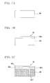
- FIGS. 1 and 2 are front cross-sectional views illustrating a silicon substrate in each step, which is subjected to a manufacturing method of a silicon substrate related to this embodiment.
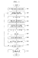
- FIG. 3 is a flowchart illustrating the manufacturing method of a silicon substrate according to this embodiment.
- a symbol W0 denotes a silicon substrate.
- a design for a silicon substrate used for manufacturing of a CCD (solid-state imaging device) and a CMOS image sensor (CIS) is described.
- the manufacturing method of the embodiment includes, as illustrated in FIG. 3 , a WS condition setting step S01 of setting a white spot condition described later, a device heat treatment condition setting step S02, an epi condition setting step S03, an IG condition setting step S04, a calculating step S05, a parameter determining step S06, a single crystal pulling step S07 for determining a fitting parameter, an evaluation device manufacturing step S08, a WS performance measuring step S09, a determining step S10, and a condition determining step S11.
- silicon substrate used in the embodiment as described later, carbon is doped, predetermined dopants corresponding to a resistivity are doped, and an initial oxygen concentration is controlled, as a silicon single crystal is pulled by a CZ method.
- the silicon single crystal is subjected to a wafer manufacturing step, thereby obtaining a silicon substrate W0 containing carbon as illustrated in FIG. 1A .
- a dopant (B) is added during the single crystal growth so that the resistivity of the silicon substrate W0 is of a p + type.
- a p + type of a boron (B) concentration corresponds to a resistivity of 8 to 10 m ⁇ cm
- a p type thereof corresponds to a resistivity of 0.1 to 100 ⁇ cm
- a p - type thereof corresponds to a resistivity of 0.1 to 0.01 ⁇ cm.
- a p/p - type is a wafer in which a p-type epitaxial layer is formed on a p - -type substrate.
- an epitaxial layer W0a is formed on the silicon substrate W0 thereby forming a p/p + -type silicon substrate W1, and as illustrated in FIG. 1C , an oxide film W0b and additionally a nitride film W0c are formed as needed on the epitaxial layer W0a of the silicon substrate W1 thereby forming a silicon wafer W2 to be provided for the device manufacturing step.
- the thickness of the epitaxial layer W0a is preferably in the range of 2 to 10 ⁇ m in terms of improvement of spectral sensitivity characteristics of a device in the case where the device is a solid-state imaging device.
- a buried photodiode is formed at the epitaxial layer of the silicon wafer W2, thereby obtaining a solid-state imaging device.
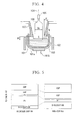
- heat treatment conditions in the device step for obtaining the solid-state imaging device 10 illustrated in FIG. 2F correspond to the respective conditions illustrated in FIG. 6 .
- the conditions are set so that the silicon substrate described above becomes a substrate suitable for the solid-state imaging device.
- a white spot condition representing upper and lower limits of the density of white spots (WS), which is an acceptable range of solid-state imaging device characteristics, is set.
- the density of white spots has a different range depending on a manufactured solid-state imaging device. For example, when 10 5 to 10 6 pieces/cm 2 is accepted, this range is used to set the upper and lower limits, and particularly, the upper limit is associated with gettering.
- the heat treatment condition is a heat treatment condition which corresponds to each condition in the device step illustrated in FIG. 6 , a forming condition of the oxide film W0b, a forming condition of the nitride film W0c, or a heat treatment condition of pre-annealing.
- This heat treatment condition which includes a processing temperature, a processing time, a rate of temperature increase, a rate of temperature decrease, and a treatment atmosphere gas has effects on the behavior of an oxygen deposit BMD in the pulled single crystal or the silicon substrate (wafer).
- the forming condition of the epitaxial layer W0a is set.
- the processing temperature, the processing time, a rate of temperature increase, the rate of temperature decrease, and the treatment atmosphere gas, which have effects on the behavior of the oxygen deposit BMD in the pulled single crystal or the silicon substrate (wafer) are also considered.
- the thicknesses of the epitaxial layer W0a, the oxide film W0b, and the nitride film W0c which have effects on the generation of dark current be considered as the forming condition.
- the BMD density and the BMD size of the silicon substrate W0 as a condition setting the gettering capability thereof are set.
- an occurrence of heavy metal contamination on the substrate surface is assumed to show the gettering capability needed to satisfy the white spot condition represented by the upper and lower limits in the WS condition setting step S01, and the range is set so that the white spots do not occur even though the heavy metal is diffused by the subsequent heat treatment.
- the condition is set to reduce the surface contamination down to a detection limit (1 ⁇ 10 10 atoms/cm 2 for Ni, 1 ⁇ 10 9 atoms/cm 2 for Cu) after the heat treatment conditions as shown in FIG. 6 .
- the BMD size of the silicon substrate W0 can be determined to be in the range of 10 to 100 nm, and the BMD density can be determined to be in the range of 1.0 ⁇ 10 06 to 1.0 ⁇ 10 11 pieces/cm 3 .
- pulling process conditions including initial oxygen concentration Oi, a carbon concentration Cs, resistivity p, and a pulling temperature condition Te (crystal thermal history), are calculated.
- the behavior of an oxygen deposit is calculated based on the behavior of an oxygen deposit nucleus in the pulled single crystal and a thermal history in the following treatment, to obtain the pulling process condition to determine a desired oxygen deposit state.
- the pulling conditions such as increasing the values in the respective ranges at every 1/10 interval for example, are set.
- the single crystal pulling step S07 for determining a fitting parameter illustrated in FIG. 3 under a plurality of the pulling conditions including the initial oxygen concentration Oi, the carbon concentration Cs, the resistivity p, and the pulling temperature condition Te determined in the parameter determining step S06, a plurality of silicon single crystals are pulled using the CZ method. Otherwise, silicon single crystals are pulled changing crystal lengths and pulling conditions so that substrates (wafers) satisfying the plurality of the pulling conditions can be cut therefrom.
- wafers are cut from the silicon single crystal pulled in the single crystal pulling step S07 for determining a fitting parameter, and on the surface of the wafer, an evaluation device having a circuit for device performance evaluation according to white spots is formed as a solid-sate imaging device.
- the circuit for evaluation is the device unit illustrated in FIG. 2 or forms a pn junction measuring a dark current.
- a MOS capacitor for example, having a gate insulating film made of a SiO 2 film having a thickness of 20 nm and a gate electrode made of an Al film, and means for forming a CCD imaging sensor on an epitaxial substrate may also be employed.
- the density of white spots in the evaluation device manufactured in the evaluation device manufacturing step S08 is measured.
- the measurement may be performed by a method of measuring the density of white spots from leak current of a photodiode. For example, the number of white spots per unit area or the number of white spots per unit device on the entire surface of the silicon substrate may be measured.
- the measurement result of the WS performance measuring step S09 is evaluated.
- the measurement result is compared with the white spot condition set in the WS condition setting step S01.
- the pulling condition under which the evaluation device is formed is destroyed, and the process returns to the device heat treatment condition setting step S02 to reset the fitting parameter and calculate and reset the pulling condition.
- the following condition determining step S11 is performed.
- the determining step S10 in the case where the number WS of white spots, measured when the initial oxygen concentration, the carbon concentration Cs, and the like are applied in the WS performance measuring step S09, is equal to or less than the upper limit WS-u of the white spot condition set in the WS condition setting step S01 within the range, Cs-t of the pulling condition as illustrated in FIG. 7 , it is determined that the range Cs-t of the pulling condition satisfies the white spot condition. In addition, it is determined that the range in which the number WS of white spots is equal to or greater than the upper limit WS-u, does not satisfy the white spot condition.
- the pulling condition (carbon concentration) Cs-m in which the number WS of white spots is at the minimum value WSmin may be determined as the optimal value satisfying the white spot condition.
- upper and lower ranges of the carbon concentration optimal value Cs-m may be determined as the pulling condition range satisfying the white spot condition. The upper and lower ranges of the optimal value Cs-m may be about ⁇ 10% thereof.
- the internal state of the silicon substrate which is provided to the solid-state imaging device to be manufactured which depends on the pulling process conditions such as the initial oxygen concentration Oi, the carbon concentration Cs, the resistivity p, a vacancy density distribution, interstitial silicon density distribution, distribution of OSF generation state, COP generable area distribution, the pulling speed V, the pulling temperature Te, a thermal history of the single crystal, a temperature gradient G, an applied magnetic condition, and an atmosphere gas condition, is determined.
- condition of the silicon substrate provided for manufacturing the solid-state imaging device can be designed by the device manufacturing conditions to obtain a needed gettering capability.
- the silicon substrate W0 as illustrated in FIG. 1A In order to manufacture the silicon substrate W0 as illustrated in FIG. 1A , first, polysilicon that is the raw material of a silicon crystal is placed in a quartz crucible, an adequate amount of graphite powder is applied to the surface of the polysilicon. Simultaneously B (boron) at a concentration corresponding to the p + type is added as a dopant, and a CZ crystal with added carbon is pulled in a hydrogen atmosphere by, for example, the Czochralski method (CZ method).
- the CZ crystal means a crystal that is manufactured by the Czochralski method and includes a magnetic field-applied CZ crystal.
- a P-type silicon single crystal containing boron is manufactured as follows. Carbon is added to a raw material, and a silicon single crystal is produced from raw material with added carbon. In addition, the oxygen concentration Oi is controlled as the silicon single crystal is pulled. Now, the pulling of the high-concentration boron CZ silicon single crystal with added carbon will be described.
- a wafer having a diameter of 300 mm is described.
- the invention is not limited thereto.
- FIG. 4 is a longitudinal cross-sectional view illustrating a CZ furnace suitable to describe a method of producing a silicon single crystal according to this embodiment.
- the CZ furnace includes a crucible (quartz crucible) 101 disposed at the center in a chamber and a heater 102 disposed outside the crucible 101.
- the crucible 101 has a double structure in which a graphite crucible 101a on the outer side retains the quartz crucible 101 accommodating a raw material melt 103, and the crucible 101 is rotated and moved up and down by a supporting shaft 101b called a pedestal.
- a cylindrical thermal shield 107 is provided above the crucible 101.
- the thermal shield 107 has a structure in which the outer shell is made of graphite, and the inner part is filled with graphite felt.
- the inner surface of the thermal shield 107 is formed as a tapered surface having a diameter that is gradually reduced from the upper end to the lower end.
- the upper outer surface of the thermal shield 107 is also formed as a tapered surface corresponding to the tapered inner surface, and the lower outer surface thereof is formed as a substantially straight (vertical) surface such that the thickness of the thermal shield 107 is gradually increased from the upper direction to the lower direction.
- the CZ furnace can grow a 300-mm single crystal having a target diameter of, for example, 310 mm and a body length of, for example, 1200 mm.
- the thermal shield 107 has the following dimensions.
- the outside diameter of a portion that is placed inside the crucible is, for example, 570 mm
- the minimum inside diameter S of the lowermost portion is, for example, 370 mm
- the width (thickness) W of the thermal shield 107 in the radial direction is, for example, 100 mm
- the inclination angle of the inner surface of an inverted truncated cone in the vertical direction is, for example, 21°.
- the inside diameter of the crucible 101 is, for example, 650 mm
- a height H of the lower end of the thermal shield 107 from a melt surface is, for example, 60 mm.
- a dopant (B) is added at a concentration that allows the resistivity of the crystal to correspond to a p + type.
- a dopant is added to a silicon melt so that the carbon concentration is within a predetermined range.
- the crystal rotation speed, the crucible rotation speed, the heating conditions, the applied magnetic field conditions, and the pulling speed are controlled to obtain a predetermined initial oxygen concentration.
- the internal pressure of the furnace is set to be in the range of 1.33 to 26.7 kPa (10 to 200 torr) in an inert gas atmosphere, which is a reduced pressure range.
- hydrogen gas is mixed with an inert gas (for example, Ar gas) to occupy a 3 to 20 volume% and introduced into the furnace.
- the pressure is equal to or higher than 1.33 kPa (10 torr), preferably, in the range of 4 to 26.7 kPa (30 to 200 torr), and more preferably, in the range of 4 to 9.3 kPa (30 to 70 torr).
- the lower limit of the pressure when the partial pressure of hydrogen is reduced, the concentration of hydrogen in the melt and crystal is reduced, and thus, in order to prevent the reduction of the hydrogen concentration, the lower limit of the pressure is defined.
- the upper limit of the pressure when the internal pressure of the furnace is increased, the gas flow rate in the melt of an inert gas such as Ar is decreased. Then, the reactant gas such as carbon released from a carbon heater or a carbon member and SiO evaporated from the melt, cannot be easily removed.
- the concentration of carbon in the crystal is increased to be higher than a desired value, and SiO is agglutinated at an inner portion of the furnace that is above the melt and has a temperature of about 1100°C or less and dust is generated and falls into the melt. As a result, crystal dislocation may occur. Therefore, in order to prevent the above problems, the upper limit of the pressure is defined.
- silicon is heated and melted by the heater 102 to obtain a melt 103.
- a seed crystal held by a seed chuck 105 is dipped into the melt 103, and the crystal is pulled as the crucible 101 and a pulling shaft 104 are rotated. Any one of the ⁇ 100 ⁇ , ⁇ 111 ⁇ , and ⁇ 110 ⁇ -oriented crystals is used, and seed narrowing is performed to prevent dislocation-free crystallization.
- a shoulder portion is formed, and the shoulder portion is changed to obtain a target body diameter of, for example, 310 mm.
- a body portion having a length of, for example, 1200 mm is grown at a constant pulling speed, and tail narrowing is performed to reduce the diameter of the body portion in normal conditions, thereby completing the crystal growth.
- the pulling speed is appropriately determined depending on, for example, resistivity, the diameter of the silicon single crystal, and a hot zone structure (thermal environment) of the single crystal pulling apparatus used.
- a pulling speed including the range in which an OSF ring is generated on a single crystal surface may be employed.
- the lower limit of the pulling speed may be determined to be equal to or higher than the pulling speed at which the OSF ring region is generated on the single crystal surface but a dislocation cluster is not generated.
- the concentration of hydrogen in the inert atmosphere may be set to be equal to or higher than 3% and equal to or lower than 20% at the internal pressure of the furnace that is in the range of 4.0 to 9.33 kPa (30 to 70 torr).
- the internal pressure of the furnace is equal to or higher than 1.33 kPa (10 torr), preferably, in the range of 4.0 to 26.7 kPa (30 to 200 torr), and more preferably, in the range of 4.0 to 9.3 kPa (30 to 70 torr).
- the lower limit of the pressure is defined.
- the upper limit when the internal pressure of the furnace is increased, the gas flow rate in the melt of the inert gas such as Ar is decreased. Then, a reactant gas such as carbon released from a carbon heater or a carbon member and SiO evaporated from the melt, cannot be easily exhausted. In this case, the concentration of carbon in the crystal is increased to be higher than a desired value, and SiO is agglutinated at an inner portion of the furnace that is above the melt and has a temperature of about 1100°C or less and dust is generated and falls into the melt. As a result, crystal dislocation may occur. Therefore, in order to prevent the above problems, the upper limit of the pressure is defined. It is preferable that the partial pressure of hydrogen be equal to or higher than 40 Pa and equal to or lower than 400 Pa.
- the concentration of hydrogen in the silicon single crystal can be controlled by the partial pressure of hydrogen in the atmosphere.
- hydrogen in the atmosphere is dissolved in a silicon melt and becomes a normal (equilibrium) state.
- hydrogen concentrations in a liquid phase and a solid phase are distributed by concentration segmentation during congelation.
- the concentration of hydrogen in a melt is determined depending on the partial pressure of hydrogen in a gas phase by Henry's law.
- concentration of hydrogen in the crystal immediately after congelation can be controlled to a desired constant value in the axial direction of the crystal by controlling the partial pressure of hydrogen in the atmosphere.
- the silicon single crystal growth method since a silicon single crystal is pulled in an inert atmosphere containing hydrogen, COP and a dislocation cluster are not included in the entire region of a crystal in the diametric direction.
- the single crystal is pulled while widening the range of a PI region pulling speed capable of pulling a single crystal in an interstitial silicon-dominated region (PI region), a straight portion of the single crystal can become the interstitial silicon-dominated region (PI region) without a dislocation cluster.
- the width of the OSF ring is reduced.
- the PI region pulling speed needs to be set in a very narrow range.
- the PI region pulling speed range in a hydrogen atmosphere is compared with that in an inert atmosphere without hydrogen under the conditions in which the value of a temperature gradient G in the axial direction of a crystal immediately after congelation does not vary.
- the PI region pulling speed range capable of pulling a grown-in defect-free single crystal that is composed of an interstitial-silicon-type grown-in defect-free region (PI region) is four times or more that in the atmosphere without hydrogen.
- the PI region pulling speed range can be enlarged to have a margin that is 4.5 times that to perform pulling, thereby pulling a desired single crystal at a pulling speed.
- PV region vacancy-type grown-in defect-free region
- the addition of hydrogen makes it easy to pull a grown-in defect-free single crystal
- the addition of carbon makes it possible to reduce the influence of the OSF ring. Therefore, when an epitaxial layer is grown on the wafer, defects caused by the OSF ring can be reduced and a single crystal with desired quality can be pulled by the synergistic effect of the addition of hydrogen and the addition of carbon. As a result, operating efficiency is improved, and it is possible to significantly reduce the manufacturing cost of a silicon single crystal or a silicon substrate manufactured from the silicon single crystal, which is preferable.
- the silicon substrate W0 containing carbon as illustrated in FIG. 1A is obtained from the pulled carbon-added high-concentration boron CZ silicon single crystal.
- a general method is performed to process the silicon substrate (wafer) W0.
- a cutting apparatus such as an ID saw and a wire saw is used to slice a silicon single crystal to obtain a silicon wafer.
- annealing is performed on the obtained silicon wafer, and then surface treatments such as polishing and cleaning are performed thereon.
- there are various steps such as wrapping, cleaning, and grinding. The order of the processes may be changed, and the processes may be appropriately omitted for the purpose of use.
- the obtained silicon substrate I has a boron (B) concentration corresponding to a p + type.
- the carbon concentration is in the range of 1.0 ⁇ 10 16 to 1.6 ⁇ 10 17 atoms/cm 3
- the oxygen concentration is in the range of 1.4 ⁇ 10 18 to 1.6 ⁇ 10 18 atoms/cm 3 .
- the concentration of carbon added in the above-mentioned range needs to be regulated. This is because when the carbon concentration is lower than the above-mentioned range, the formation of an oxygen/carbon-based deposit is not accelerated and the above-mentioned high-density oxygen/carbon-based deposit cannot be formed.
- the silicon substrate W0 which is a carbon-added CZ crystal
- RCA cleaning which is a combination of, for example, SC1 and SC2 is performed thereon.
- an epitaxial layer forming step in order to grow an epitaxial layer, the silicon substrate W0 is put into an epitaxial growth furnace, and various CVD (chemical vapor deposition) methods are used to grow an epitaxial layer W0a having a boron (B) concentration corresponding to the p type, thereby obtaining the p/p + -type silicon substrate W1 as illustrated in FIG. 1B .
- CVD chemical vapor deposition
- the oxide film W0b and the nitride film W1c may be additionally formed on the epitaxial layer W0a as needed, thereby obtaining the silicon wafer W2.
- the silicon substrate W0 of the silicon substrate W1 or W2 provided in the device manufacturing step is a CZ crystal containing boron and solute carbon.
- an oxygen deposit nucleus or an oxygen deposit formed in the CZ crystal during crystal growth is shrunken by heat treatment when epitaxial growth is performed. Therefore, the oxygen deposit formed in the silicon substrate W0 in the stage of the silicon substrate W1 is not observed by an optical microscope.
- a low-temperature heat treatment is performed preferably at a temperature between 600 and 800°C for 0.25 to 3 hours, thereby allowing a boron/carbon/oxygen-based oxygen deposit W07 to deposit from carbon at a substitution position.
- the boron/carbon/oxygen-based deposit means a complex (cluster) containing boron/carbon.
- the oxygen deposit W07 is spontaneously deposited from the entire silicon substrate W0 in an initial stage of the device manufacturing step. Therefore, it is possible to form gettering sinks having high gettering capability for metal contamination in the device manufacturing step over the entire thickness of the silicon substrate W0 from immediately below the epitaxial layer. As a result, gettering is performed near the epitaxial layer.
- the oxygen deposit (BMD) W07 which is the complex includes boron, carbon, and oxegen, have a size in the range of 10 to 100 nm and a density in the range of 1.0 ⁇ 10 6 to 1.0 ⁇ 10 11 pieces/cm 3 in the silicon substrate W0.
- the size of the oxygen deposit W07 is equal to or greater than the lower limit of the above-mentioned range, it is possible to increase the probability of gettering interstitial impurities (for example, heavy metal) using the effect of strain occurring in an interface between a maternal silicon atom and the oxygen deposit.
- the size of the oxygen deposit W07 is equal to or greater than the above-mentioned range, the strength of the substrate is degraded or dislocation occurs in the epitaxial layer, which is not preferable.
- the density of the oxygen deposit W07 in the silicon substrate be in the above-mentioned range because the gettering of heavy metal in the silicon crystal depends on strain occurring in the interface between the maternal silicon atom and the oxygen deposit and an interface level density (volume density).
- a general solid-state imaging device manufacturing process can be employed as the device step.
- a CCD manufacturing process is illustrated in FIG. 2 , but the invention is not limited thereto.
- the silicon substrate 3 having the p-type silicon substrate 1 and the p-type epitaxial layer 2 formed on the silicon substrate 1 as illustrated in FIG. 1B is prepared, and a first n-type well region 11 is formed at a predetermined position of the epitaxial layer 2 as illustrated in FIG. 2B . Thereafter, as illustrated in FIG.
- a gate insulating film 12 is formed thereon, and n-type and p-type impurities are selectively implanted into the first n-type well region 11 by ion implantation to form a p-type transmission channel region 13, an n-type channel stop region 14, and a second n-type well region 15, thereby constituting a vertical transmission register.
- transmission electrodes 16 are formed at predetermined positions on the surface of the gate insulating film 12.
- p-type and n-type impurities are selectively implanted between the p-type transmission channel region 13 and the second n-type well region 15 to form a photodiode 19 having a laminated structure of an n-type positive charge storage region 17 and a p-type impurity diffusion region 18.
- an interlayer insulating film 20 is formed thereon, and a light-shielding film 21 is formed on the surface of the interlayer insulating film 20 except for a portion immediately above the photodiode 19, thereby manufacturing a silicon substrate W3 as a solid-state imaging device 10.
- the heat treatment conditions of the device step for manufacturing the solid-state imaging device 10 correspond to the respective conditions illustrated in FIG. 6 .
- Initial, Step 1, Step 2, Step 3, Step 4, and Step 5 illustrated in FIG. 6 correspond to the end times of steps of a process of forming the photodiode and the transmission transistor.
- a heat treatment is generally performed at a temperature between 600 to 1000°C during, for example, a gate oxide film forming step, a device separating step, a polysilicon gate electrode forming step, and the like.
- the heat treatment makes it possible to deposit the oxygen depositW07 described above, and the oxygen deposit can function as a gettering sink in the subsequent step, thereby showing the gettering capability without pre-annealing.
- the thickness of the epitaxial layer W0a be in the range of 2 to 10 ⁇ m in terms of improvement of the spectral sensitivity characteristics of a device when the device is a solid-state imaging device.
- a buried photodiode is formed at the epitaxial layer W0a of the silicon wafer W2, thereby obtaining the solid-state imaging device.
- the thicknesses of the oxide film W0b and the nitride film W0c be determined in consideration of restrictions in the design of the driving voltage of a transmission transistor. Specifically, it is preferable that the thickness of the oxide film W0b be in the range of 50 to 100 nm. In addition, it is preferable that the thickness of the nitride film W0c, specifically, the polysilicon gate film W1b of the solid-state imaging device be in the range of 1.0 to 2.0 ⁇ m.
- the heat treatment be performed as pre-annealing before the device manufacturing step, it is preferable that the heat treatment be performed at a temperature between 600 and 800°C for 0.25 to 3 hours in a mixed atmosphere of oxygen and an inert gas such as argon or nitrogen. Accordingly, the heat treatment makes it possible to give an 1G (gettering) effect to the silicon substrate.
- the heat treatment step is not necessarily needed for a high-concentration boron substrate and can be omitted.
- the temperature and the processing time of the heat treatment are equal to or higher than those of a temperature of 600°C and a processing time of 30 minutes and may be changed as long as the same precipitation effect as that under this condition can be obtained.
- the temperature and the process time of the heat treatment are equal to or lower than those in a condition of a temperature of 800°C and a processing time of 4 hours and may be changed as long as the same precipitation effect as that under this condition can be obtained.
- the order for calculating pulling process conditions including the initial oxygen concentration Oi, the carbon concentration Cs, the resistivity p, and the pulling temperature condition Te of the silicon single crystal under pulling, from the conditions set in the WS condition setting step S01, the device heat treatment condition setting step S02, the epi condition setting step S03, and the IG condition setting step S04, by using the Fokker-Planck equation, will be described.
- a pseudo-equilibrium distribution function f 0 (r,t) is employed.
- P in the equation (8) is considered as a variable influenced by a thermal history during the crystal pulling step and other impurities than oxygen and therefore treated as a fitting parameter for fitting the calculation result into an experimental result. Therefore, in order to obtain P, the result of the single crystal pulling step S07 for determining a fitting parameter is applied to calculate f 0 (r,t).
- pulling process conditions including the initial oxygen concentration Oi, the carbon concentration Cs (dopant concentration), the resistivity p, and the pulling temperature condition Te (crystal thermal history) of the silicon single crystal under pulling, is obtained to reach a desired oxygen deposit and internal defect density during or after a particular wafer step, an oxygen deposit, the initial oxygen concentration dependency of internal defect density, the dopant concentration or resistivity dependency, and the crystal thermal history dependency.
- a condition of the single crystal manufacturing step subjected to the Czochralski method including the initial oxygen concentration, the dopant concentration or resistivity, and the heat treatment condition can be determined simply and clearly so as to obtain a silicon wafer having a desired gettering capability.
- a numerical computation program using a model in which free energy during the formation of a silicon oxide, and more specifically, strain energy depend on a dopant concentration or a resistivity may be executed to enhance precision.
- the wafer can be used for, for example, a multi chip package (MCP) such as NAND-FLASH and NOR-FLASH.
- MCP multi chip package
- the device structure is CMOS
- determination setting of dark current in the evaluation device is changed for adaptation. Therefore, the design for the silicon substrate subjected to the manufacturing method of the invention can be adapted. Accordingly, it is possible to provide a silicon substrate capable of maintaining a high gettering capability.
- the p + -type is preferable for the silicon substrate in terms of device designing. Specifically, a phenomenon in which a floating charge that may occur during the operation of a device drives a undesired parasitic transistor, that is, so-called a latchup, is prevented by using the p + wafer (silicon substrate), and the design for the device can be easy. In addition, when a trench-structure capacitor is used, an extension of a depletion layer around the trench, which occurs when a voltage is applied, can be prevented by the p + wafer.
- the inventors analyzed and examined the states and behaviors of carbon, oxygen, and boron.
- the examination results proved that when a wafer was manufactured from a silicon single crystal that was pulled under the conditions of a boron (B) concentration corresponding to a resistivity of 8 to 10 m ⁇ cm, a carbon concentration of 0.5 ⁇ 10 16 to 1.6 ⁇ 10 17 atoms/cm 3 , and an oxygen concentration of 1.4 ⁇ 10 18 to 1.6 ⁇ 10 18 atoms/cm 3 , and an epitaxial layer was formed on the wafer and subjected to the heat treatment at a temperature between 600 and 800°C, it was possible to manufacture a silicon substrate having sufficient BMD size and density to form gettering sinks required to getter heavy metal and achieve sufficient gettering capability.
- B boron
- a new p + substrate containing a high-concentration of boron can accelerate precipitation without performing heat treatment.
- gettering sinks having carbon, boron, or oxygen as nuclei are fonned during a crystal growth process. These gettering sinks stably exist even when a high-temperature heat treatment is performed. Therefore, these gettering sinks exist even after epitaxial growth.
- oxide deposits act as deposit nuclei immediately after epitaxial growth, and the nuclei are grown during the device heat treatment step and serve as gettering sinks for heavy metal contamination during the device heat treatment step.
- the manufacturing method may include: a step of pulling a silicon single crystal having a B concentration corresponding to a resistivity of 8 to 10 m ⁇ cm, a C concentration of 0.5 ⁇ 10 16 to 1.6 ⁇ 10 17 atoms/cm 3 , and an oxygen concentration of 1.4 ⁇ 10 18 to 1.6 ⁇ 10 18 atoms/cm 3 by using the CZ method; and a heat treatment step of performing heat treatment to form an oxygen deposit on a silicon substrate sliced from the pulled silicon single crystal.
- the heat treatment for forming the oxygen deposit may be performed at a temperature between 600 and 800°C, a processing time of 0.25 to 3 hours, in a mixed atmosphere of oxygen and an inert gas such as argon or nitrogen.
- a step of forming a silicon epitaxial layer having a B concentration corresponding to a resistivity of 0.1 to 100 ⁇ cm on the surface of the obtained silicon substrate may be included.
- hydrogen when the silicon single crystal is grown, hydrogen may be added to an inert gas atmosphere.
- the pressure of the inert gas atmosphere having hydrogen added thereto may be in a range of 1.33 to 26.7 kPa, which is a reduced pressure range, and the concentration of hydrogen gas in the atmosphere may be in the range of 3 to 20 volume%.
- a silicon substrate of a solid-state imaging device is a silicon device in which a gettering layer having a BMD size of 10 to 100 nm and a BMD density of 1.0 ⁇ 10 6 to 1.0 ⁇ 10 11 pieces/cm 3 is formed at a position immediately below a buried photodiode of the solid-state imaging device.
- a silicon epitaxial layer having a B concentration corresponding to a resistivity of 0.1 to 100 ⁇ cm is formed immediately above the silicon substrate manufactured by the manufacturing method.
- the gettering layer may be formed immediately below the epitaxial layer.
- the vicinity of carbon at an lattice point of Si is distorted, thereby forming a strain field.
- DK donor killer
- the heat treatment of the device manufacturing step is performed on the substrate in this state, interstitial oxygen is gathered on the strain field in the vicinity of the carbon-oxygen pair, thereby forming BMD.
- carbon is doped on the silicon substrate at the device region or a position closer to the wafer surface where heavy metal contamination easily occurs, and the vicinity of the carbon is distorted, heavy metal diffuses to be gettered. As a result, the gettering effect can be obtained.
- the carbon-oxygen pair becomes a nucleus generation center (new creation center) of the oxygen deposit.
- complexes of carbon-oxygen, boron-oxygen, carbon-boron, and carbon-boron-oxygen, and many complexes in which those complexes are associated with silicon are formed. These complexes also have strain fields similarly to the carbon-oxygen pair, so that all of the pairs and the complexes become deposit nuclei. Specifically, since many strain fields can be formed on the highly-doped substrate, an overwhelming number of deposit nuclei exist when compared with a substrate having a B concentration corresponding to p - . Therefore, the density of deposits to serve as the gettering sink overwhelmingly increase.
- the precipitation nucleus is a complex defect due to boron/carbon/oxygen.
- the p/p + -type silicon substrate serves as the silicon substrate for a device sensitive to heavy metal contamination due to the high gettering capability.
- flatness of the silicon substrate affects device reservation, so that high flatness is required.
- the silicon substrate is the p + substrate which is doped with C and has a high B concentration, PBS that degrades the flatness is not formed, and it is possible to obtain sufficient gettering capability.
- the sufficient gettering capability needs to be exhibited before the device manufacturing step is started and to be maintained during the device step. Therefore, in the manufacturing step of the p-type silicon substrate, when C is not doped, in order to enhance precipitation, it is preferable that the oxygen concentration Oi be increased to be in the range of 10 to 20 ⁇ 10 18 atoms/cm 3 . However, when the oxygen concentration in the substrate is increased, there is a concern that epi defects in which a dislocation extends to the epitaxial layer may occur. On the other hand, as in the embodiment of the invention, the above-mentioned concentration of carbon is doped. Therefore, there is an advantage in that generation of stacking fault (SF) of equal to or greater than 0.5 ⁇ m can be suppressed.
- SF stacking fault
- a deposit having a size of 0.5 to 5 ⁇ m has a secondary dislocation that occurs in the vicinity of a strain field in order to release the generated strain.
- a number of deposits having sizes of 0.5 to 100 nm can be formed. Therefore, although strain is released, only a small secondary dislocation occurs. As a result, the dislocation does not extend to the epitaxial layer.
- a number of small deposit nuclei exist at a concentration of about 1.0 ⁇ 10 10 to 1.0 ⁇ 10 13 /cm 3 . Therefore, it is possible to exhibit sufficient gettering capability.
Landscapes
- Chemical & Material Sciences (AREA)
- Engineering & Computer Science (AREA)
- Crystallography & Structural Chemistry (AREA)
- Materials Engineering (AREA)
- Metallurgy (AREA)
- Organic Chemistry (AREA)
- Physics & Mathematics (AREA)
- Thermal Sciences (AREA)
- Crystals, And After-Treatments Of Crystals (AREA)
- Solid State Image Pick-Up Elements (AREA)
- Testing Or Measuring Of Semiconductors Or The Like (AREA)
Applications Claiming Priority (1)
| Application Number | Priority Date | Filing Date | Title |
|---|---|---|---|
| JP2008054842A JP5343371B2 (ja) | 2008-03-05 | 2008-03-05 | シリコン基板とその製造方法 |
Publications (3)
| Publication Number | Publication Date |
|---|---|
| EP2099073A2 EP2099073A2 (en) | 2009-09-09 |
| EP2099073A3 EP2099073A3 (en) | 2013-06-19 |
| EP2099073B1 true EP2099073B1 (en) | 2015-07-29 |
Family
ID=40637142
Family Applications (1)
| Application Number | Title | Priority Date | Filing Date |
|---|---|---|---|
| EP09003141.0A Active EP2099073B1 (en) | 2008-03-05 | 2009-03-04 | Manufacturing method of a silicon substrate |
Country Status (5)
| Country | Link |
|---|---|
| US (1) | US8864907B2 (https=) |
| EP (1) | EP2099073B1 (https=) |
| JP (1) | JP5343371B2 (https=) |
| KR (1) | KR101208651B1 (https=) |
| TW (1) | TWI412083B (https=) |
Families Citing this family (11)
| Publication number | Priority date | Publication date | Assignee | Title |
|---|---|---|---|---|
| JP2010010615A (ja) * | 2008-06-30 | 2010-01-14 | Sumco Corp | 固体撮像素子用シリコン基板およびその製造方法 |
| KR101464566B1 (ko) * | 2013-02-21 | 2014-11-24 | 주식회사 엘지실트론 | 실리콘 웨이퍼 |
| JP6302216B2 (ja) * | 2013-11-08 | 2018-03-28 | ルネサスエレクトロニクス株式会社 | 半導体装置およびその製造方法 |
| US11111602B2 (en) | 2014-07-31 | 2021-09-07 | Globalwafers Co., Ltd. | Nitrogen doped and vacancy dominated silicon ingot and thermally treated wafer formed therefrom having radially uniformly distributed oxygen precipitation density and size |
| JP6531729B2 (ja) * | 2016-07-19 | 2019-06-19 | 株式会社Sumco | シリコン試料の炭素濃度評価方法、シリコンウェーハ製造工程の評価方法、シリコンウェーハの製造方法およびシリコン単結晶インゴットの製造方法 |
| JP6579086B2 (ja) * | 2016-11-15 | 2019-09-25 | 信越半導体株式会社 | デバイス形成方法 |
| US10522367B2 (en) * | 2017-03-06 | 2019-12-31 | Qualcomm Incorporated | Gettering layer formation and substrate |
| JP6702268B2 (ja) * | 2017-06-15 | 2020-05-27 | 信越半導体株式会社 | エピタキシャルウェーハの製造方法 |
| JP7415889B2 (ja) * | 2020-11-17 | 2024-01-17 | 株式会社Sumco | X線センサ向けエピタキシャルウェーハおよびx線センサ |
| JP7729256B2 (ja) * | 2022-05-11 | 2025-08-26 | 株式会社Sumco | エピタキシャルシリコンウェーハ |
| JP2025030474A (ja) * | 2023-08-23 | 2025-03-07 | 信越半導体株式会社 | エピタキシャルウェーハ及びその製造方法 |
Family Cites Families (23)
| Publication number | Priority date | Publication date | Assignee | Title |
|---|---|---|---|---|
| JP3384506B2 (ja) * | 1993-03-30 | 2003-03-10 | ソニー株式会社 | 半導体基板の製造方法 |
| JP4613886B2 (ja) * | 1993-03-30 | 2011-01-19 | ソニー株式会社 | 固体撮像素子の製造方法、及び半導体基板の製造方法 |
| JP2874834B2 (ja) * | 1994-07-29 | 1999-03-24 | 三菱マテリアル株式会社 | シリコンウェーハのイントリンシックゲッタリング処理法 |
| JPH08104592A (ja) * | 1994-08-09 | 1996-04-23 | Sony Corp | 半導体装置用半導体基板と半導体装置との製造方法 |
| JP3533783B2 (ja) * | 1995-10-18 | 2004-05-31 | ソニー株式会社 | 半導体基板および半導体装置の各製造方法 |
| JP3324469B2 (ja) * | 1997-09-26 | 2002-09-17 | 信越半導体株式会社 | Soiウエーハの製造方法ならびにこの方法で製造されるsoiウエーハ |
| JPH11103042A (ja) * | 1997-09-26 | 1999-04-13 | Sony Corp | 固体撮像装置用半導体基板と固体撮像装置の製造方法 |
| JP3144378B2 (ja) * | 1998-04-01 | 2001-03-12 | 日本電気株式会社 | 固体撮像装置の製造方法 |
| JP3279527B2 (ja) * | 1998-08-24 | 2002-04-30 | 住友金属工業株式会社 | 半導体シリコン基板におけるig能の評価方法、及び半導体シリコン基板の製造方法 |
| JP2002353434A (ja) * | 2001-05-22 | 2002-12-06 | Sony Corp | 固体撮像装置の製造方法 |
| JP3973083B2 (ja) * | 2002-02-13 | 2007-09-05 | シャープ株式会社 | 固体撮像装置、その画素不良変換方法および傷補正方法 |
| JP2003318181A (ja) * | 2002-04-25 | 2003-11-07 | Sumitomo Mitsubishi Silicon Corp | 半導体シリコン基板におけるig能の評価方法 |
| EP1780781B1 (en) | 2004-06-30 | 2019-08-07 | SUMCO Corporation | Process for producing silicon wafer |
| JP4706199B2 (ja) * | 2004-07-20 | 2011-06-22 | 株式会社Sumco | Simox基板の製造方法 |
| JP2006073580A (ja) * | 2004-08-31 | 2006-03-16 | Sumco Corp | シリコンエピタキシャルウェーハ及びその製造方法 |
| US7438760B2 (en) * | 2005-02-04 | 2008-10-21 | Asm America, Inc. | Methods of making substitutionally carbon-doped crystalline Si-containing materials by chemical vapor deposition |
| JP2006261632A (ja) * | 2005-02-18 | 2006-09-28 | Sumco Corp | シリコンウェーハの熱処理方法 |
| JP4604889B2 (ja) * | 2005-05-25 | 2011-01-05 | 株式会社Sumco | シリコンウェーハの製造方法、並びにシリコン単結晶育成方法 |
| JP4770276B2 (ja) * | 2005-06-01 | 2011-09-14 | 船井電機株式会社 | 固体撮像装置および固体撮像素子 |
| JP2007273959A (ja) * | 2006-03-06 | 2007-10-18 | Matsushita Electric Ind Co Ltd | 光検出素子及びその製造方法 |
| JP2008054842A (ja) | 2006-08-30 | 2008-03-13 | J O Phama Co Ltd | クリップ |
| CN101351890A (zh) | 2006-09-07 | 2009-01-21 | 胜高股份有限公司 | 固态图像传感装置的半导体基板以及固态图像传感装置和其制造方法 |
| JP5568837B2 (ja) | 2008-02-29 | 2014-08-13 | 株式会社Sumco | シリコン基板の製造方法 |
-
2008
- 2008-03-05 JP JP2008054842A patent/JP5343371B2/ja active Active
-
2009
- 2009-03-03 TW TW098106829A patent/TWI412083B/zh active
- 2009-03-03 KR KR1020090018227A patent/KR101208651B1/ko active Active
- 2009-03-04 EP EP09003141.0A patent/EP2099073B1/en active Active
- 2009-03-04 US US12/397,399 patent/US8864907B2/en active Active
Also Published As
| Publication number | Publication date |
|---|---|
| JP2009212353A (ja) | 2009-09-17 |
| KR101208651B1 (ko) | 2012-12-05 |
| US20090226737A1 (en) | 2009-09-10 |
| TWI412083B (zh) | 2013-10-11 |
| EP2099073A2 (en) | 2009-09-09 |
| EP2099073A3 (en) | 2013-06-19 |
| JP5343371B2 (ja) | 2013-11-13 |
| TW201001554A (en) | 2010-01-01 |
| US8864907B2 (en) | 2014-10-21 |
| KR20090095494A (ko) | 2009-09-09 |
Similar Documents
| Publication | Publication Date | Title |
|---|---|---|
| EP2099073B1 (en) | Manufacturing method of a silicon substrate | |
| KR101073419B1 (ko) | 실리콘 기판과 그 제조 방법 | |
| EP2098620A1 (en) | Method of manufacturing silicon substrate | |
| US8101508B2 (en) | Silicon substrate and manufacturing method thereof | |
| US6626994B1 (en) | Silicon wafer for epitaxial wafer, epitaxial wafer, and method of manufacture thereof | |
| JPWO2009075257A1 (ja) | シリコン基板とその製造方法 | |
| JP2025157587A (ja) | シリコンウェーハおよびエピタキシャルシリコンウェーハ | |
| JP2025146998A (ja) | シリコンウェーハおよびエピタキシャルシリコンウェーハ | |
| JPWO2009075288A1 (ja) | シリコン基板とその製造方法 | |
| JP4510997B2 (ja) | シリコン半導体基板およびその製造方法 | |
| JP7757917B2 (ja) | シリコンウェーハおよびエピタキシャルシリコンウェーハ | |
| JP2004091221A (ja) | シリコン単結晶とエピタキシャルウェーハ並びにそれらの製造方法 | |
| JP5401808B2 (ja) | シリコン基板とその製造方法 | |
| JP5401809B2 (ja) | シリコン基板とその製造方法 | |
| JP4615785B2 (ja) | 窒素添加基板を用いたエピ層欠陥のないエピタキシャルウエハの製造方法 | |
| JP7658332B2 (ja) | シリコンウェーハおよびエピタキシャルシリコンウェーハ | |
| JP7729256B2 (ja) | エピタキシャルシリコンウェーハ | |
| JP2011023533A (ja) | シリコン基板とその製造方法 |
Legal Events
| Date | Code | Title | Description |
|---|---|---|---|
| PUAI | Public reference made under article 153(3) epc to a published international application that has entered the european phase |
Free format text: ORIGINAL CODE: 0009012 |
|
| 17P | Request for examination filed |
Effective date: 20090304 |
|
| AK | Designated contracting states |
Kind code of ref document: A2 Designated state(s): AT BE BG CH CY CZ DE DK EE ES FI FR GB GR HR HU IE IS IT LI LT LU LV MC MK MT NL NO PL PT RO SE SI SK TR |
|
| AX | Request for extension of the european patent |
Extension state: AL BA RS |
|
| PUAL | Search report despatched |
Free format text: ORIGINAL CODE: 0009013 |
|
| AK | Designated contracting states |
Kind code of ref document: A3 Designated state(s): AT BE BG CH CY CZ DE DK EE ES FI FR GB GR HR HU IE IS IT LI LT LU LV MC MK MT NL NO PL PT RO SE SI SK TR |
|
| AX | Request for extension of the european patent |
Extension state: AL BA RS |
|
| RIC1 | Information provided on ipc code assigned before grant |
Ipc: C30B 15/04 20060101ALI20130516BHEP Ipc: C30B 29/06 20060101ALI20130516BHEP Ipc: H01L 27/146 20060101AFI20130516BHEP Ipc: C30B 15/20 20060101ALI20130516BHEP |
|
| RBV | Designated contracting states (corrected) |
Designated state(s): AT BE BG CH CY CZ DE DK EE ES FI FR GB GR HR HU IE IS IT LI LT LU LV MC MK MT NL NO PL PT RO SE SI SK TR |
|
| AKX | Designation fees paid |
Designated state(s): FR IT |
|
| REG | Reference to a national code |
Ref country code: DE Ref legal event code: R108 |
|
| REG | Reference to a national code |
Ref country code: DE Ref legal event code: R108 Effective date: 20140226 |
|
| 17Q | First examination report despatched |
Effective date: 20140415 |
|
| RIC1 | Information provided on ipc code assigned before grant |
Ipc: C30B 29/06 20060101ALI20150115BHEP Ipc: C30B 15/20 20060101ALI20150115BHEP Ipc: C30B 15/04 20060101ALI20150115BHEP Ipc: H01L 27/146 20060101AFI20150115BHEP Ipc: C30B 33/02 20060101ALI20150115BHEP |
|
| GRAP | Despatch of communication of intention to grant a patent |
Free format text: ORIGINAL CODE: EPIDOSNIGR1 |
|
| INTG | Intention to grant announced |
Effective date: 20150227 |
|
| GRAS | Grant fee paid |
Free format text: ORIGINAL CODE: EPIDOSNIGR3 |
|
| GRAA | (expected) grant |
Free format text: ORIGINAL CODE: 0009210 |
|
| AK | Designated contracting states |
Kind code of ref document: B1 Designated state(s): FR IT |
|
| REG | Reference to a national code |
Ref country code: FR Ref legal event code: PLFP Year of fee payment: 8 |
|
| PLBE | No opposition filed within time limit |
Free format text: ORIGINAL CODE: 0009261 |
|
| STAA | Information on the status of an ep patent application or granted ep patent |
Free format text: STATUS: NO OPPOSITION FILED WITHIN TIME LIMIT |
|
| 26N | No opposition filed |
Effective date: 20160502 |
|
| REG | Reference to a national code |
Ref country code: FR Ref legal event code: PLFP Year of fee payment: 9 |
|
| REG | Reference to a national code |
Ref country code: FR Ref legal event code: PLFP Year of fee payment: 10 |
|
| PGFP | Annual fee paid to national office [announced via postgrant information from national office to epo] |
Ref country code: IT Payment date: 20260324 Year of fee payment: 18 |
|
| PGFP | Annual fee paid to national office [announced via postgrant information from national office to epo] |
Ref country code: FR Payment date: 20260320 Year of fee payment: 18 |