EP2095544B1 - Mehrfarbige quanten-dot-laserdiode mit geringem rin für ein optisches übertragungssystem - Google Patents
Mehrfarbige quanten-dot-laserdiode mit geringem rin für ein optisches übertragungssystem Download PDFInfo
- Publication number
- EP2095544B1 EP2095544B1 EP07856278.2A EP07856278A EP2095544B1 EP 2095544 B1 EP2095544 B1 EP 2095544B1 EP 07856278 A EP07856278 A EP 07856278A EP 2095544 B1 EP2095544 B1 EP 2095544B1
- Authority
- EP
- European Patent Office
- Prior art keywords
- optical
- laser
- transmission system
- optical transmission
- active region
- Prior art date
- Legal status (The legal status is an assumption and is not a legal conclusion. Google has not performed a legal analysis and makes no representation as to the accuracy of the status listed.)
- Active
Links
Images



Classifications
-
- H—ELECTRICITY
- H01—ELECTRIC ELEMENTS
- H01S—DEVICES USING THE PROCESS OF LIGHT AMPLIFICATION BY STIMULATED EMISSION OF RADIATION [LASER] TO AMPLIFY OR GENERATE LIGHT; DEVICES USING STIMULATED EMISSION OF ELECTROMAGNETIC RADIATION IN WAVE RANGES OTHER THAN OPTICAL
- H01S5/00—Semiconductor lasers
- H01S5/30—Structure or shape of the active region; Materials used for the active region
- H01S5/34—Structure or shape of the active region; Materials used for the active region comprising quantum well or superlattice structures, e.g. single quantum well [SQW] lasers, multiple quantum well [MQW] lasers or graded index separate confinement heterostructure [GRINSCH] lasers
-
- B—PERFORMING OPERATIONS; TRANSPORTING
- B82—NANOTECHNOLOGY
- B82Y—SPECIFIC USES OR APPLICATIONS OF NANOSTRUCTURES; MEASUREMENT OR ANALYSIS OF NANOSTRUCTURES; MANUFACTURE OR TREATMENT OF NANOSTRUCTURES
- B82Y20/00—Nanooptics, e.g. quantum optics or photonic crystals
-
- H—ELECTRICITY
- H01—ELECTRIC ELEMENTS
- H01S—DEVICES USING THE PROCESS OF LIGHT AMPLIFICATION BY STIMULATED EMISSION OF RADIATION [LASER] TO AMPLIFY OR GENERATE LIGHT; DEVICES USING STIMULATED EMISSION OF ELECTROMAGNETIC RADIATION IN WAVE RANGES OTHER THAN OPTICAL
- H01S5/00—Semiconductor lasers
- H01S5/30—Structure or shape of the active region; Materials used for the active region
- H01S5/34—Structure or shape of the active region; Materials used for the active region comprising quantum well or superlattice structures, e.g. single quantum well [SQW] lasers, multiple quantum well [MQW] lasers or graded index separate confinement heterostructure [GRINSCH] lasers
- H01S5/341—Structures having reduced dimensionality, e.g. quantum wires
-
- H—ELECTRICITY
- H01—ELECTRIC ELEMENTS
- H01S—DEVICES USING THE PROCESS OF LIGHT AMPLIFICATION BY STIMULATED EMISSION OF RADIATION [LASER] TO AMPLIFY OR GENERATE LIGHT; DEVICES USING STIMULATED EMISSION OF ELECTROMAGNETIC RADIATION IN WAVE RANGES OTHER THAN OPTICAL
- H01S2301/00—Functional characteristics
- H01S2301/02—ASE (amplified spontaneous emission), noise; Reduction thereof
-
- H—ELECTRICITY
- H01—ELECTRIC ELEMENTS
- H01S—DEVICES USING THE PROCESS OF LIGHT AMPLIFICATION BY STIMULATED EMISSION OF RADIATION [LASER] TO AMPLIFY OR GENERATE LIGHT; DEVICES USING STIMULATED EMISSION OF ELECTROMAGNETIC RADIATION IN WAVE RANGES OTHER THAN OPTICAL
- H01S3/00—Lasers, i.e. devices using stimulated emission of electromagnetic radiation in the infrared, visible or ultraviolet wave range
- H01S3/05—Construction or shape of optical resonators; Accommodation of active medium therein; Shape of active medium
- H01S3/06—Construction or shape of active medium
- H01S3/063—Waveguide lasers, i.e. whereby the dimensions of the waveguide are of the order of the light wavelength
- H01S3/067—Fibre lasers
-
- H—ELECTRICITY
- H01—ELECTRIC ELEMENTS
- H01S—DEVICES USING THE PROCESS OF LIGHT AMPLIFICATION BY STIMULATED EMISSION OF RADIATION [LASER] TO AMPLIFY OR GENERATE LIGHT; DEVICES USING STIMULATED EMISSION OF ELECTROMAGNETIC RADIATION IN WAVE RANGES OTHER THAN OPTICAL
- H01S5/00—Semiconductor lasers
- H01S5/005—Optical components external to the laser cavity, specially adapted therefor, e.g. for homogenisation or merging of the beams or for manipulating laser pulses, e.g. pulse shaping
- H01S5/0078—Optical components external to the laser cavity, specially adapted therefor, e.g. for homogenisation or merging of the beams or for manipulating laser pulses, e.g. pulse shaping for frequency filtering
-
- H—ELECTRICITY
- H01—ELECTRIC ELEMENTS
- H01S—DEVICES USING THE PROCESS OF LIGHT AMPLIFICATION BY STIMULATED EMISSION OF RADIATION [LASER] TO AMPLIFY OR GENERATE LIGHT; DEVICES USING STIMULATED EMISSION OF ELECTROMAGNETIC RADIATION IN WAVE RANGES OTHER THAN OPTICAL
- H01S5/00—Semiconductor lasers
- H01S5/10—Construction or shape of the optical resonator, e.g. extended or external cavity, coupled cavities, bent-guide, varying width, thickness or composition of the active region
- H01S5/1092—Multi-wavelength lasing
- H01S5/1096—Multi-wavelength lasing in a single cavity
-
- H—ELECTRICITY
- H01—ELECTRIC ELEMENTS
- H01S—DEVICES USING THE PROCESS OF LIGHT AMPLIFICATION BY STIMULATED EMISSION OF RADIATION [LASER] TO AMPLIFY OR GENERATE LIGHT; DEVICES USING STIMULATED EMISSION OF ELECTROMAGNETIC RADIATION IN WAVE RANGES OTHER THAN OPTICAL
- H01S5/00—Semiconductor lasers
- H01S5/30—Structure or shape of the active region; Materials used for the active region
- H01S5/34—Structure or shape of the active region; Materials used for the active region comprising quantum well or superlattice structures, e.g. single quantum well [SQW] lasers, multiple quantum well [MQW] lasers or graded index separate confinement heterostructure [GRINSCH] lasers
- H01S5/341—Structures having reduced dimensionality, e.g. quantum wires
- H01S5/3412—Structures having reduced dimensionality, e.g. quantum wires quantum box or quantum dash
-
- H—ELECTRICITY
- H01—ELECTRIC ELEMENTS
- H01S—DEVICES USING THE PROCESS OF LIGHT AMPLIFICATION BY STIMULATED EMISSION OF RADIATION [LASER] TO AMPLIFY OR GENERATE LIGHT; DEVICES USING STIMULATED EMISSION OF ELECTROMAGNETIC RADIATION IN WAVE RANGES OTHER THAN OPTICAL
- H01S5/00—Semiconductor lasers
- H01S5/30—Structure or shape of the active region; Materials used for the active region
- H01S5/34—Structure or shape of the active region; Materials used for the active region comprising quantum well or superlattice structures, e.g. single quantum well [SQW] lasers, multiple quantum well [MQW] lasers or graded index separate confinement heterostructure [GRINSCH] lasers
- H01S5/343—Structure or shape of the active region; Materials used for the active region comprising quantum well or superlattice structures, e.g. single quantum well [SQW] lasers, multiple quantum well [MQW] lasers or graded index separate confinement heterostructure [GRINSCH] lasers in AIIIBV compounds, e.g. AlGaAs-laser, InP-based laser
- H01S5/34306—Structure or shape of the active region; Materials used for the active region comprising quantum well or superlattice structures, e.g. single quantum well [SQW] lasers, multiple quantum well [MQW] lasers or graded index separate confinement heterostructure [GRINSCH] lasers in AIIIBV compounds, e.g. AlGaAs-laser, InP-based laser emitting light at a wavelength longer than 1000nm, e.g. InP based 1300 and 1500nm lasers
Definitions
- the present invention relates to an optical transmission system and, more particularly, to an optical transmission system that uses a plurality of optical signals at different wavelengths.
- WDM wavelength-division-multiplexing
- Modulating and detecting each channel independently is also required in order to carry information by means of an optical signal.
- a multiple modulated wavelength source based on a Fabry-Perot laser diode is known from US-A-2003/0 165 173 .
- a laser diode source emitting radiation at multiple wavelengths with low overall RIN is known from US-A-2004/0 057 485 .
- Quantum dot laser diodes with inhomogeneously broadened amplification bandwidth are known from JP Reithmaier et al., IEEE J. of Sel. Topics in Quant. Electron. 8 (2002) 1035 .
- An optical transmission system includes a Fabry-Perot semiconductor diode laser, a transmitter and a receiver.
- the laser operates in a continuous-wave regime on an inhomogeneously broadened optical transition of the active region of the laser.
- a spectral bandwidth of an output lasing spectrum of the laser is greater than 5nm and a spectral power density of the laser is greater than 2mW/nm such that an optical power of the laser is greater than 10mW.
- the laser provides a plurality of longitudinal modes of the resonator, i.e. a plurality of optical signals at different wavelengths.
- a relative intensity noise (RIN) of at least ten longitudinal modes does not exceed -120 dB /Hz at 0.1GHz, - 130 dB /Hz at 1.0GHz and -140 dB /Hz at 10GHz.
- the transmitter is capable of providing modulation to each lasing wavelength independently and the receiver is capable of providing detection to each lasing wavelength independently.
- the laser may further include a bandpass filter in order to restrict the spectral range of emission to a desired number of optical channels.
- a laser based on an active region with an inhomogeneously broadened optical transition achieves a broad spectrum of the laser emission in combination with sufficiently high spectral power density.
- the temporal stability of spectral distribution of the emitted optical power may be very high and a relative intensity noise may be sufficiently low. This allows splitting an output spectrum into several independent optical channels and manipulating them separately for the use in a WDM system.
- the active region is an array of semiconductor quantum dots formed by self-organization phenomena in epitaxial growth.
- a conventional laser for example a semiconductor diode laser based on a quantum well, is sometimes capable of providing a relatively broad optical spectrum. This is termed multi-frequency laser operation, when the laser emits a number of longitudinal modes of the resonator.
- multi-frequency laser operation when the laser emits a number of longitudinal modes of the resonator.
- the spectral bandwidth is typically only a few nanometers. Therefore, it is difficult to split such a spectrum into many channels.
- temporal stability of a spectral distribution of the optical power is very low (i.e. RIN of a longitudinal mode is high). Therefore, a split optical channel is very noisy.
- the first limitation comes from the fact that, in the active region of a conventional laser, there exists a fast rate of carrier capture and relaxation to the energy levels. As a result, an optical gain saturation is not very pronounced and a tendency to lase at several longitudinal modes is apparent to a lesser degree.
- the second limitation is due to a competition between different longitudinal modes for a common gain (mode partition noise) because the laser medium is homogeneously broadened.
- the laser is based on an active region with an increased time of energy relaxation and inhomogeneously broadened optical transition. It is possible to achieve a broad spectrum of the laser emission in combination with sufficiently high spectral power density.
- the temporal stability of spectral distribution of the emitted optical power can be very high, i.e. a relative intensity noise can be sufficiently low. This allows splitting an output spectrum into several independent optical channels and manipulating them separately for the use in a WDM system.
- Such an active region is an array of semiconductor quantum dots formed by self-organization phenomena in epitaxial growth.
- quantum dot electronic states of different energy within an inhomogeneously broadened ground-state level belong to spatially separated quantum dots having different sizes, shapes or other parameters which affect the quantum energy. Therefore, in a quantum dot laser, only a certain portion of the available quantum dots contributes to the lasing process, namely those quantum dots which have an optical transition energy approximately equal to the lasing transition.
- Other quantum dots act as a reservoir providing charge carriers to the lasing dots.
- a high degree of temporal stability in such a laser system means that an optical power of each split optical channel remains stable for a long period of time which makes it possible to achieve low levels of noise and acceptable error bit rates.
- This improvement in temporal stability likely originates from being able to easily saturate the optical gain of an inhomogeneously broadened active region.
- the laser operates in a regime of the saturated gain in a significant part of the spectrum, there is no possibility for different longitudinal modes to compete for a gain. Therefore, the optical gain in a significant part of the spectrum remains at its saturated level being stable in time. This results in high stability of intensities of emitted longitudinal modes. In one embodiment, this results in high stability of intensities of a multimode laser, for example a Fabry-Perot laser.
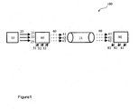
- the transmission system 100 includes a laser 10, a transmitter 60 and a receiver 90.
- the laser emits a plurality 20 of optical signals at different wavelengths. In Figure 1 , only three different wavelengths are illustrated by numerals 21, 22, 23. However, it is preferred that the laser emits more optical signals at different wavelengths.
- the laser may further include a bandpass filter, for example a distributed Bragg reflector, in order to restrict a number of emitting longitudinal modes to a desired number of optical channels.
- the laser 10 operates in a continuous-wave (CW) mode such that the intensities of the optical signals 21, 22, 23 are nearly constant in time.
- the intensities of optical signals 21, 22, 23 at different wavelengths are also preferably nearly equal to each other.
- the transmitter 60 may include waveguides, modulators, as well as lenses, prisms, arrayed waveguide gratings, and other standard optical components.
- the waveguides, modulators, and other optical components of the transmitter 60 are preferably embedded into a semiconductor chip.
- the semiconductor chip is preferably based on a material including, but not limited to, silicon, gallium arsenide, or indium phosphide.
- the optical signals 20 enter the transmitter 60.
- the transmitter is capable of providing modulation to each lasing wavelength independently in response to a plurality of control signals 51, 52, 53.
- the transmitter 60 outputs a plurality 40 of the intensity modulated optical signals 41, 42, and 43 at different wavelengths. It is preferred that the number of modulated optical signals 41, 42, and 43 corresponds to a number of CW optical signals 21, 22, and 23, while their wavelengths remain unchanged.
- the optical transmission system 100 may further include a transmission line 15 that is intended to guide the modulated optical signals 41, 42, and 43 at different wavelengths outputted from the transmitter 60 to the receiver 90.
- the transmission line 15 may include optical fibers, planar waveguides, mirrors, lenses and other standard optical components suitable for guiding the light.
- the receiver 90 may include waveguides and detectors as well as lenses, prisms, arrayed waveguide gratings, and other standard optical components.
- the waveguides, detectors, and other optical components of the receiver 90 are preferably embedded into a semiconductor chip.
- the semiconductor chip is preferably based on a material including, but not limited to, silicon, gallium arsenide, or indium phosphide.
- the plurality 40 of the intensity modulated optical signals enter the receiver 90.
- the receiver 90 is capable of providing detection to each lasing wavelength independently. As a result, the receiver 90 extracts as many information signals 81, 82, and 83 as different wavelengths are inputted.
- FIGS 2a and 2b schematically illustrate a spectrum of a plurality of CW optical signals 21, 22, and 23 and temporal variation of their intensity.
- the laser emits a plurality of optical signals at different wavelengths ⁇ 1, ⁇ 2 and ⁇ 3.
- Each optical signal represents a single longitudinal mode.
- Figure 1 , Figure 2a and Figure 2b illustrate only three different wavelengths.
- the laser preferably emits more optical signals at different wavelengths. Neighboring different wavelengths are preferably equally spaced.
- the intensities of the optical signals 21, 22, 23 are nearly constant in time and the intensities of the optical signals 21, 22, 23 are nearly equal to each other.
- Figures 2c and 2d schematically illustrate a spectrum of a plurality of intensity modulated optical signals 41, 42, and 43 and temporal variation of their intensity.
- the set of wavelengths ⁇ 1, ⁇ 2 and ⁇ 3 remains unchanged while the intensities of the optical signals 41, 42, and 43 are modulated in time in accordance with carrying information.
- Figure 2d schematically shows that the intensity of an optical signal at certain wavelengths (e.g. of optical signal 41 at wavelength ⁇ 1) is encoded.
- the high intensity of signal 41 may correspond to level “1" of a binary sequence and the low intensity of signal 41 may correspond to level "0" of a binary sequence.
- signal 42 at wavelength ⁇ 2 can be modulated independently, signal 42 (and other signals at other wavelengths) may carry another sequence of binary codes, thereby providing an additional information bearing channel.
- the laser 10 is capable of operating on an inhomogeneously broadened ground-state optical transition of the active region of the laser.
- the laser 100 is a semiconductor diode laser.
- the active region of the laser includes a plurality of semiconductor quantum dots embedded in a semiconductor matrix having fluctuations in a parameter affecting the optical transition energy, including, but not limited to, solely or in combination: size, shape, chemical composition, strain and matrix.
- the active region of the laser includes a plurality of two-dimensional quantum wells in a semiconductor matrix having fluctuations in a parameter affecting the optical transition energy, including, but not limited to, solely or in combination: thickness, chemical composition, compositional profile, strain and matrix.
- the laser is a fiber laser and the active region of the laser includes a plurality of ions embedded in a fiber core having fluctuations in a parameter affecting the optical transition energy, including, but not limited to, solely or in combination: chemical composition, degree of ionization and the distance between neighboring ions.
- lasers may be used in the system 100, provided that the laser 10 is capable of operating on an inhomogeneously broadened ground-state optical transition of the active region of the laser.
- the laser may optionally include active regions with any combination of quantum dots and quantum wells.
- a spectral bandwidth of an output lasing spectrum of the laser 10 is preferably greater than 10nm and a spectral power density of the laser 10 is preferably greater than 3mW/nm such that an optical power of the laser 10 is preferably greater than 30mW.
- a laser based on self-organized quantum dots is disclosed in U.S. patent application number 11/737,946, filed April 20, 2007 , entitled "LASER SOURCE WITH BROADBAND SPECTRUM EMISSION".
- the laser represents an edge-emitting Fabry-Perot laser in a pigtailed package.
- a pigtailed package is a standard laser package having an optical fiber for outputting the laser radiation.
- Different wavelengths ⁇ 1, ⁇ 2, and ⁇ 3 correspond to different longitudinal modes of the Fabry-Perot resonator of the laser.
- the laser 10 may further include a bandpass filter in order to restrict a number of emitting longitudinal modes to a desired number of optical channels.
- the laser 10 provides a plurality 20 of optical signals at different wavelengths.
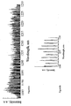
- Figure 3a shows an example of an experimental emission spectrum of a semiconductor laser according to an embodiment of the present invention.
- the active region of the laser represents an array of self-organized InAs/InGaAs quantum dots with inhomogeneously broadened optical transitions due to fluctuation of the quantum dot size.
- the laser in this example operates in a CW regime at 25°C with a total optical power of 300mW at a pump current of 550mA.
- the laser spectrum ranges from approximately 1184nm to approximately 1228nm so that the spectral bandwidth is approximately 44nm and the average spectral power density is approximately 6.8 mW/nm.
- the spectrum includes a number of longitudinal modes separated from each other by approximately 0.2 nm. Therefore, the laser spectrum may include as many as approximately 220 longitudinal modes. An average optical power of one longitudinal mode is therefore greater than 1.3 mW.
- relative intensity noise spectra for several longitudinal modes of a broadband quantum-dot Fabry-Perot laser was measured to demonstrate high temporal stability of optical channels.
- the laser active region represents ten non-identical planes of self-organized quantum dots.
- Each quantum dot plane was formed by epitaxial deposition of 0.8nm-thick InAs insertions covered with In 0.15 Ga 0.85 As capping layers and embedded into a GaAs matrix.
- the epitaxial wafer was processed into 3- ⁇ m-wide ridge structures.
- the cavity length is approximately 1 mm as terminated by as-cleaved facets forming two laser mirrors.
- the laser was driven by a forward CW current of 85mA, which is 5-times above the lasing threshold.
- a separation between neighboring longitudinal modes is 0.22nm.
- the laser emission bandwidth was restricted to 2nm (from 1264 to 1266nm) in order to include 10 longitudinal modes.
- the average spectral power density of the laser was -25mW/nm (total power is 50mW), and an average optical power per one channel was more than 2 mW.
- FIG. 4a shows a filtered intensity of one of the longitudinal modes. In this case, as well as for other filtered modes, side mode suppression ratio is -20dB.
- Figure 4b shows frequency dependence of relative intensity noise for one optical channel. The relative intensity noise is approximately -120 dB /Hz at 0.1GHz, -133 dB /Hz at 1.0GHz and -140 dB /Hz at 10GHz. Such a very low level of the relative intensity noise for a single wavelength line makes it suitable for an independent optical channel of a multi-channel transmission system.
- Bit error rate and an eye diagram were measured for ten spectrally filtered optical channels to show that the optical source of the present invention is compatible with a highspeed WDM application.
- the channel intensity was externally modulated at 10Gb/s by a 2 31 -1 pseudorandom binary non-return-to-zero sequence using a pulse pattern generator and a lithium niobate digital modulator.
- Figure 5a shows an eye diagram for the 1265.48nm mode at -3dBm received power.
- Figure 5a shows an "open eye", i.e. no error points in the central region.
- An open eye pattern corresponds to minimal signal distortion.
- Table 1 shows some of the data obtained from the eye diagram of Figure 5a .
- the extinction ratio is defined as the ratio P 1 /P 0 , where P 1 is the optical power level generated when the light source is "on,” and P 0 is the power level generated when the light source is “off.”
- Figure 5a corresponds to an extinction ratio of approximately 7dB, which is sufficient for use in WDM applications.
- the column labeled "current” includes data from a particular reading.
- the column labeled “minimum” includes the minimum values obtained during the experiment and the column labeled "maximum” includes the maximum values obtained during the experiment.
- the Q-factor depends on the laser noise and the noise of the other elements of the system (modulator noise, photodetector noise, electronics noise, oscilloscope noise, etc.).
- FIG. 5b shows an eye diagram generated by a 10Gb/s digital modulation of a single-frequency emission of a prior-art laser.
- Table 2 shows some of the data obtained from the eye diagram of Figure 5b .
- a Q-factor of 11.8 was measured with a similar extinction ratio of approximately 7dB.
Landscapes
- Physics & Mathematics (AREA)
- Optics & Photonics (AREA)
- Engineering & Computer Science (AREA)
- Condensed Matter Physics & Semiconductors (AREA)
- General Physics & Mathematics (AREA)
- Electromagnetism (AREA)
- Nanotechnology (AREA)
- Chemical & Material Sciences (AREA)
- Biophysics (AREA)
- Crystallography & Structural Chemistry (AREA)
- Life Sciences & Earth Sciences (AREA)
- Semiconductor Lasers (AREA)
- Optical Communication System (AREA)
Claims (7)
- Optisches Übertragungssystem (100), umfassend:a) einen Fabry-Perot-Halbleiter-Diodenlaser (10), der einen aktiven Bereich und einen Resonator umfasst, wobei der aktive Bereich eine Vielzahl von Halbleiter-Quantenpunkten umfasst, die in einer Halbleitermatrix eingebettet sind, die Schwankungen in einem Parameter aufweist, der die optische Übertragungsenergie beeinflusst;
wobei der Laser in einem Dauerstrichbetrieb an einem inhomogen verbreiterten optischen Übergang des aktiven Bereichs funktioniert;
wobei der Laser geeignet ist, um eine spektrale Bandbreite eines Ausgangslaserspektrums, die größer als 5 nm ist, und eine spektrale Leistungsdichte, die größer als 2 mW/nm ist, bereitzustellen, so dass eine optische Leistung des Lasers größer als 10 mW ist;
wobei der Laser geeignet ist, um eine Vielzahl von optischen Signalen (20) bei verschiedenen Wellenlängen bereitzustellen, wobei jedes der optischen Signale einen longitudinalen Mode des Resonators darstellt, so dass ein relatives Intensitätsrauschen jedes von mindestens zehn longitudinalen Moden nicht über -120 dB/Hz auf 0,1 GHz, -130 dB/Hz auf 1,0 GHz und -140 dB/Hz auf 10 GHz hinausgeht;b) einen Sender (60), der geeignet ist, um eine Modulation für jedes optische Signal unabhängig bereitzustellen; undc) einen Empfänger (90), der geeignet ist, um eine Detektion für jedes modulierte optische Signal unabhängig bereitzustellen. - Optisches Übertragungssystem nach Anspruch 1, wobei der Parameter, der die optische Übergangsenergie beeinflusst, aus der Gruppe gewählt wird, die besteht aus:a) Größe;b) Form;c) chemischer Zusammensetzung;d) Spannung; unde) Matrix; undf) mindestens einem von a) bis e).
- Optisches Übertragungssystem nach Anspruch 1 oder 2, ferner umfassend ein Bandpassfilter, das geeignet ist, um eine Breite eines Emissionsspektrums des Lasers auf eine gewünschte Anzahl von optischen Signalen einzuschränken.
- Optisches Übertragungssystem nach einem der Ansprüche 1 bis 3, wobei der Sender mindestens einen Wellenleiter und mindestens einen Modulator umfasst, die in einen ersten Halbleiterchip eingebettet sind, und der Empfänger mindestens einen Wellenleiter und mindestens einen Detektor umfasst, die in einen zweiten Halbleiterchip eingebettet sind.
- Optisches Übertragungssystem nach Anspruch 4, wobei der erste Halbleiterchip ein Material umfasst, das aus der Gruppe ausgewählt wird, die aus: Silizium, Galliumarsenid und Indiumphosphid besteht.
- Optisches Übertragungssystem nach Anspruch 4, wobei der zweite Halbleiterchip ein Material umfasst, das aus der Gruppe ausgewählt wird, die aus: Silizium, Galliumarsenid und Indiumphosphid besteht.
- Optisches Übertragungssystem nach einem der Ansprüche 1 bis 6, ferner umfassend eine Übertragungsleitung, die geeignet ist, um die optischen Signale von dem Sender zu dem Empfänger zu führen.
Applications Claiming Priority (3)
| Application Number | Priority Date | Filing Date | Title |
|---|---|---|---|
| US86795206P | 2006-11-30 | 2006-11-30 | |
| US11/938,472 US7835408B2 (en) | 2005-12-07 | 2007-11-12 | Optical transmission system |
| PCT/EP2007/010313 WO2008064874A1 (en) | 2006-11-30 | 2007-11-28 | Multicolour quantum dot laser diode with low rin for optical transmission system |
Publications (2)
| Publication Number | Publication Date |
|---|---|
| EP2095544A1 EP2095544A1 (de) | 2009-09-02 |
| EP2095544B1 true EP2095544B1 (de) | 2014-10-22 |
Family
ID=39099796
Family Applications (1)
| Application Number | Title | Priority Date | Filing Date |
|---|---|---|---|
| EP07856278.2A Active EP2095544B1 (de) | 2006-11-30 | 2007-11-28 | Mehrfarbige quanten-dot-laserdiode mit geringem rin für ein optisches übertragungssystem |
Country Status (3)
| Country | Link |
|---|---|
| US (1) | US7835408B2 (de) |
| EP (1) | EP2095544B1 (de) |
| WO (1) | WO2008064874A1 (de) |
Families Citing this family (3)
| Publication number | Priority date | Publication date | Assignee | Title |
|---|---|---|---|---|
| EP2371044B1 (de) | 2008-12-03 | 2019-08-28 | Innolume GmbH | Halbleiterlaser mit geringem relativem intensitätsrauschen individueller longitudinalmoden und den laser umfassendes optisches übertragungssystem |
| US11960130B2 (en) | 2021-01-22 | 2024-04-16 | Ram Photonics Industrial, Llc | Method and system for stabilizing fiber grating optical parameters |
| WO2022159796A1 (en) * | 2021-01-22 | 2022-07-28 | Ram Photonics, LLC | Method and system for multi-wavelength laser system |
Family Cites Families (104)
| Publication number | Priority date | Publication date | Assignee | Title |
|---|---|---|---|---|
| JPS51128280A (en) * | 1975-04-30 | 1976-11-09 | Hitachi Ltd | Optical bonding semiconojctor device and its mandfactoring metho |
| US4368481A (en) * | 1979-06-19 | 1983-01-11 | Tokyo Shibaura Denki Kabushiki Kaisha | Light-driven semiconductor device |
| US5298787A (en) * | 1979-08-10 | 1994-03-29 | Massachusetts Institute Of Technology | Semiconductor embedded layer technology including permeable base transistor |
| GB2105544B (en) * | 1981-09-01 | 1985-03-27 | Standard Telephones Cables Ltd | Multiplexing of optical signals |
| US4438447A (en) * | 1982-01-18 | 1984-03-20 | Bell Telephone Laboratories, Incorporated | Multilayered optical integrated circuit |
| FR2562328B1 (fr) * | 1984-03-30 | 1987-11-27 | Menigaux Louis | Procede de fabrication d'un dispositif optique integre monolithique comprenant un laser a semi-conducteur et dispositif obtenu par ce procede |
| JPS61160987A (ja) * | 1985-01-09 | 1986-07-21 | Nec Corp | 集積型半導体光素子とその製造方法 |
| US4734910A (en) * | 1987-03-25 | 1988-03-29 | Bell Communications Research, Inc. | Self mode locked semiconductor laser diode |
| US4989201A (en) * | 1987-06-09 | 1991-01-29 | At&T Bell Laboratories | Optical communication system with a stabilized "comb" of frequencies |
| US4839884A (en) * | 1988-03-04 | 1989-06-13 | General Electric Company | Multiple wavelength optical source and multiplexed light communication system |
| DE3835601A1 (de) * | 1988-10-19 | 1990-05-03 | Messerschmitt Boelkow Blohm | Digitalrechner mit einer multiprozessor-anordnung |
| US4918497A (en) * | 1988-12-14 | 1990-04-17 | Cree Research, Inc. | Blue light emitting diode formed in silicon carbide |
| GB8904781D0 (en) * | 1989-03-02 | 1989-04-12 | British Telecomm | Apparatus for and method of generating a comb of optical teeth of different wavelengths |
| US4959540A (en) * | 1989-05-15 | 1990-09-25 | International Business Machines Corporation | Optical clock system with optical time delay means |
| US4980568A (en) | 1989-05-22 | 1990-12-25 | Hewlett-Packard Company | Optical isolator having high voltage isolation and high light flux light guide |
| FR2662304B1 (fr) * | 1990-05-21 | 1992-07-24 | France Telecom | Procede de fabrication d'une structure integree guide-detecteur de lumiere en materiau semi-conducteur. |
| JP2689698B2 (ja) * | 1990-07-19 | 1997-12-10 | 国際電信電話株式会社 | αパラメータ符号を反転させた半導体素子 |
| JP3003944B2 (ja) * | 1990-10-04 | 2000-01-31 | オリンパス光学工業株式会社 | 固体撮像素子 |
| JPH04163967A (ja) * | 1990-10-27 | 1992-06-09 | Canon Inc | 光デバイス |
| US5274649A (en) * | 1990-11-21 | 1993-12-28 | Kabushiki Kaisha Toshiba | Wavelength-tunable distributed-feedback semiconductor laser device |
| SE468027B (sv) * | 1991-02-27 | 1992-10-19 | Asea Brown Boveri | Optoelektronisk komponent med halvledarelement innefattade i sluten kapsel, vilken kapsel bestaar av en kaapa som centreras och laases relativt en sockel medelst ett byggelement |
| FR2676126B1 (fr) * | 1991-04-30 | 1993-07-23 | France Telecom | Dispositif optoelectronique a guide optique et photodetecteur integres. |
| US5357122A (en) * | 1991-09-05 | 1994-10-18 | Sony Corporation | Three-dimensional optical-electronic integrated circuit device with raised sections |
| US5265112A (en) * | 1991-09-27 | 1993-11-23 | Siemens Aktiengesellschaft | Optical comb generator |
| US5214664A (en) * | 1991-10-18 | 1993-05-25 | Xerox Corporation | Multiple wavelength semiconductor laser |
| EP0567693A1 (de) * | 1992-04-27 | 1993-11-03 | BRITISH TELECOMMUNICATIONS public limited company | Optische Taktrückgewinnung |
| CA2096551A1 (en) * | 1992-05-22 | 1993-11-23 | Masanori Nishiguchi | Semiconductor device |
| EP0582986B1 (de) * | 1992-08-10 | 1999-01-20 | Canon Kabushiki Kaisha | Halbleitervorrichtung und Herstellungsverfahren |
| FR2694841B1 (fr) * | 1992-08-14 | 1994-09-09 | Commissariat Energie Atomique | Procédé d'hybridation et de positionnement d'un composant opto-électronique et application de ce procédé au positionnement de ce composant par rapport à un guide optique intégré. |
| US5673140A (en) | 1992-09-08 | 1997-09-30 | British Telecommunications Public Limited Company | Non-linear semiconductor optical device |
| DE69421434T2 (de) * | 1993-04-07 | 2000-06-08 | Mitsui Chemicals, Inc. | Leiterplatte für optische Elemente |
| JPH0794833A (ja) * | 1993-09-22 | 1995-04-07 | Mitsubishi Electric Corp | 半導体レーザおよびその製造方法 |
| JP3635683B2 (ja) * | 1993-10-28 | 2005-04-06 | ソニー株式会社 | 電界効果トランジスタ |
| JP3234086B2 (ja) * | 1994-01-18 | 2001-12-04 | キヤノン株式会社 | 光半導体デバイス及びその製造方法 |
| US5705831A (en) * | 1994-04-07 | 1998-01-06 | Matsushita Electric Industrial Co., Ltd. | Semiconductor light-emitting device and production method thereof, and crystal-growing method suitable for the production method |
| FR2719159B1 (fr) * | 1994-04-26 | 1996-06-14 | Adrien Bruno | Dispositif optoélectronique intégrant un photodétecteur à deux diodes. |
| US6064783A (en) * | 1994-05-25 | 2000-05-16 | Congdon; Philip A. | Integrated laser and coupled waveguide |
| US5710436A (en) * | 1994-09-27 | 1998-01-20 | Kabushiki Kaisha Toshiba | Quantum effect device |
| SE503416C2 (sv) * | 1994-10-25 | 1996-06-10 | Asea Brown Boveri | Optoelektrisk komponent samt förfarande för montering av en sådan |
| US5802084A (en) * | 1994-11-14 | 1998-09-01 | The Regents Of The University Of California | Generation of high power optical pulses using flared mode-locked semiconductor lasers and optical amplifiers |
| JPH08172217A (ja) | 1994-12-19 | 1996-07-02 | Fujitsu Ltd | 光半導体装置 |
| EP0723302B1 (de) | 1995-01-23 | 2001-08-22 | AGENCY OF INDUSTRIAL SCIENCE & TECHNOLOGY MINISTRY OF INTERNATIONAL TRADE & INDUSTRY | Lichtempfängliche Vorrichtung |
| US5633527A (en) * | 1995-02-06 | 1997-05-27 | Sandia Corporation | Unitary lens semiconductor device |
| JP2809124B2 (ja) * | 1995-02-09 | 1998-10-08 | 日本電気株式会社 | 光半導体集積素子およびその製造方法 |
| US5568499A (en) * | 1995-04-07 | 1996-10-22 | Sandia Corporation | Optical device with low electrical and thermal resistance bragg reflectors |
| JPH08330608A (ja) * | 1995-05-29 | 1996-12-13 | Oki Electric Ind Co Ltd | 受光センサおよび受発光センサ |
| GB9517927D0 (en) | 1995-09-01 | 1995-11-01 | Imperial College | Optoelectrically gated microstructure |
| US5699378A (en) * | 1995-10-06 | 1997-12-16 | British Telecommunications Public Limited Company | Optical comb filters used with waveguide, laser and manufacturing method of same |
| US5940424A (en) * | 1996-06-24 | 1999-08-17 | International Business Machines Corporation | Semiconductor lasers and method for making the same |
| DE19638667C2 (de) * | 1996-09-20 | 2001-05-17 | Osram Opto Semiconductors Gmbh | Mischfarbiges Licht abstrahlendes Halbleiterbauelement mit Lumineszenzkonversionselement |
| JP2822994B2 (ja) | 1996-09-11 | 1998-11-11 | 日本電気株式会社 | モード同期半導体レーザ |
| US6043515A (en) | 1996-09-17 | 2000-03-28 | Kabushiki Kaisha Toshiba | Optical semiconductor device |
| JPH118442A (ja) * | 1996-10-07 | 1999-01-12 | Canon Inc | 光半導体デバイス、それを用いた光通信システム及び方法 |
| DE19642168A1 (de) | 1996-10-12 | 1998-04-16 | Preh Elektro Feinmechanik | Optoelektronisches Bauelement |
| US6031243A (en) | 1996-10-16 | 2000-02-29 | Geoff W. Taylor | Grating coupled vertical cavity optoelectronic devices |
| FR2756384B1 (fr) | 1996-11-28 | 1999-02-12 | Minot Christophe | Dispositif bidirectionnel de transposition entre des signaux optiques et des signaux electriques, pour systeme de communication |
| US5854804A (en) | 1996-12-13 | 1998-12-29 | Intel Corporation | Method and apparatus for synchronizing a mode locked laser with a device under test |
| US5812708A (en) | 1996-12-31 | 1998-09-22 | Intel Corporation | Method and apparatus for distributing an optical clock in an integrated circuit |
| FR2760101B1 (fr) * | 1997-02-24 | 1999-04-16 | Alsthom Cge Alcatel | Procede d'assemblage d'un dispositif opto-hybride |
| JP3033517B2 (ja) * | 1997-04-17 | 2000-04-17 | 日本電気株式会社 | 半導体波長可変レーザ |
| DE19730830A1 (de) * | 1997-07-18 | 1999-01-21 | Alsthom Cge Alcatel | Laser zur Erzeugung eines Wellenkamms |
| US6232142B1 (en) * | 1997-12-09 | 2001-05-15 | Seiko Epson Corporation | Semiconductor device and method for making the same, electro-optical device using the same and method for making the electro-optical device, and electronic apparatus using the electro-optical device |
| US6066860A (en) * | 1997-12-25 | 2000-05-23 | Seiko Epson Corporation | Substrate for electro-optical apparatus, electro-optical apparatus, method for driving electro-optical apparatus, electronic device and projection display device |
| US6320204B1 (en) * | 1997-12-25 | 2001-11-20 | Seiko Epson Corporation | Electro-optical device in which an extending portion of a channel region of a semiconductor layer is connected to a capacitor line and an electronic apparatus including the electro-optical device |
| TW486581B (en) * | 1998-01-06 | 2002-05-11 | Seiko Epson Corp | Semiconductor device, substrate for electro-optical device, electro-optical device, electronic equipment, and projection display apparatus |
| US6201638B1 (en) * | 1998-01-23 | 2001-03-13 | University Technology Corporation | Comb generating optical cavity that includes an optical amplifier and an optical modulator |
| GB2334141A (en) * | 1998-01-30 | 1999-08-11 | Northern Telecom Ltd | Semiconductor device packaging |
| DE29805392U1 (de) * | 1998-03-25 | 1999-08-05 | Dr. Johannes Heidenhain Gmbh, 83301 Traunreut | Optoelektronische Baugruppe |
| US6661816B2 (en) * | 1998-06-11 | 2003-12-09 | University Of Central Florida | Multiwavelength modelocked lasers |
| EP0977063A1 (de) * | 1998-07-28 | 2000-02-02 | Interuniversitair Micro-Elektronica Centrum Vzw | Steckerbuchse und System für optoelektronische Verbindung und deren Herstellungsverfahren |
| US6393183B1 (en) * | 1998-08-13 | 2002-05-21 | Eugene Robert Worley | Opto-coupler device for packaging optically coupled integrated circuits |
| FI105588B (fi) * | 1998-12-10 | 2000-09-15 | Nokia Mobile Phones Ltd | Parannettu valolähdejärjestely tasomaisiin sovelluksiin |
| JP2000332348A (ja) * | 1999-05-24 | 2000-11-30 | Oki Electric Ind Co Ltd | モード同期半導体レーザ |
| KR100325687B1 (ko) * | 1999-12-21 | 2002-02-25 | 윤덕용 | 주입된 비간섭성 광에 파장 잠김된 페브리-페롯 레이저다이오드를 이용한 파장분할 다중방식 광통신용 광원 |
| JP4719331B2 (ja) * | 2000-03-10 | 2011-07-06 | 富士通株式会社 | 波長多重光信号処理装置 |
| WO2001088993A2 (en) * | 2000-05-19 | 2001-11-22 | Mcmaster University | A METHOD FOR LOCALLY MODIFYING THE EFFECTIVE BANDGAP ENERGY IN INDIUM GALLIUM ARSENIDE PHOSPHIDE (InGaAsP) QUANTUM WELL STRUCTURES |
| US6826205B1 (en) * | 2000-05-22 | 2004-11-30 | Lightwave Electronics Corporation | Etalon enhanced saturable reflector for mode-locked lasers |
| ATE346410T1 (de) * | 2000-08-04 | 2006-12-15 | Amberwave Systems Corp | Siliziumwafer mit monolithischen optoelektronischen komponenten |
| US6768754B1 (en) * | 2000-09-13 | 2004-07-27 | National Research Council Of Canada | Quantum dot tunable external cavity lasers (QD-TEC lasers) |
| US6600169B2 (en) * | 2000-09-22 | 2003-07-29 | Andreas Stintz | Quantum dash device |
| US6816525B2 (en) * | 2000-09-22 | 2004-11-09 | Andreas Stintz | Quantum dot lasers |
| JP4789319B2 (ja) * | 2000-11-22 | 2011-10-12 | 富士通株式会社 | レーザダイオードおよびその製造方法 |
| WO2002082602A2 (en) * | 2001-02-28 | 2002-10-17 | The Research Foundation Of State University Of New York | Semiconductor laser with reduced temperature sensitivity |
| WO2002071142A1 (en) * | 2001-03-02 | 2002-09-12 | Nagoya Industrial Science Research Institute | Wideband light spectrum generator and pulse light generator |
| WO2002071562A2 (en) * | 2001-03-02 | 2002-09-12 | Science & Technology Corporation @ Unm | Quantum dot vertical cavity surface emitting laser |
| US20030015720A1 (en) * | 2001-07-18 | 2003-01-23 | Motorola, Inc. | Structure and method for fabricating a printed circuit board utilizing a semiconductor structure and an embedded waveguide |
| JP2003109773A (ja) * | 2001-07-27 | 2003-04-11 | Semiconductor Energy Lab Co Ltd | 発光装置、半導体装置およびそれらの作製方法 |
| US6822982B2 (en) * | 2001-09-28 | 2004-11-23 | The Furukawa Electric Co., Ltd. | Device and method for providing a tunable semiconductor laser |
| US6628686B1 (en) * | 2001-11-16 | 2003-09-30 | Fox-Tek, Inc | Integrated multi-wavelength and wideband lasers |
| JP2003283036A (ja) * | 2001-12-27 | 2003-10-03 | Furukawa Electric Co Ltd:The | 半導体レーザモジュールおよびこれを用いたラマン増幅器 |
| US20030165173A1 (en) | 2002-03-01 | 2003-09-04 | Helbing Rene P. | Multiple modulated wavelengths in a compact laser |
| WO2003081733A2 (en) * | 2002-03-19 | 2003-10-02 | Bookham Technology Plc | Tunable laser |
| US6701049B1 (en) * | 2002-03-22 | 2004-03-02 | The United States Of America As Represented By The National Security Agency | Optical clock recovery device using non-linear optical waveguides |
| US20040057485A1 (en) * | 2002-07-16 | 2004-03-25 | The Furukawa Electric Co., Ltd. | Semiconductor laser device, semiconductor laser module, and optical fiber amplifier |
| US6879610B2 (en) | 2002-09-27 | 2005-04-12 | Sarnoff Corporation | Narrow spectral width light emitting devices |
| KR100469736B1 (ko) * | 2002-11-21 | 2005-02-02 | 삼성전자주식회사 | 다파장 레이징 광원에 파장 잠김된 페브리-페롯 레이저장치 및 이를 이용한 광 전송장치 |
| AU2003304482A1 (en) * | 2002-12-09 | 2005-04-11 | The Johns Hopkins University | Method and apparatus for single-photon source and quantum memory |
| US20040228564A1 (en) * | 2003-02-11 | 2004-11-18 | Luxtera, Inc. | External cavity laser source |
| KR100547866B1 (ko) * | 2003-03-05 | 2006-01-31 | 삼성전자주식회사 | 온도변화에 무관하게 페브리-페롯 레이저의 파장잠김을유지하는 방법 및 이를 이용한 파장분할다중방식 광원 |
| KR20060025188A (ko) * | 2003-06-27 | 2006-03-20 | 어플라이드 머티어리얼스, 인코포레이티드 | 낮은 지터를 갖는 펄스형 양자 도트 레이저 시스템 |
| KR100539928B1 (ko) * | 2003-08-29 | 2005-12-28 | 삼성전자주식회사 | 다파장 광원 및 그를 이용한 파장 분할 다중 시스템 |
| US20060227825A1 (en) * | 2005-04-07 | 2006-10-12 | Nl-Nanosemiconductor Gmbh | Mode-locked quantum dot laser with controllable gain properties by multiple stacking |
| TWI318815B (en) * | 2006-12-20 | 2009-12-21 | Ind Tech Res Inst | Multiwavelength semiconductor laser array and method of manufacturing the same |
| JP4427067B2 (ja) * | 2007-02-20 | 2010-03-03 | 富士通株式会社 | 光波形整形素子 |
-
2007
- 2007-11-12 US US11/938,472 patent/US7835408B2/en active Active
- 2007-11-28 EP EP07856278.2A patent/EP2095544B1/de active Active
- 2007-11-28 WO PCT/EP2007/010313 patent/WO2008064874A1/en not_active Ceased
Also Published As
| Publication number | Publication date |
|---|---|
| US20080180674A1 (en) | 2008-07-31 |
| WO2008064874A1 (en) | 2008-06-05 |
| US7835408B2 (en) | 2010-11-16 |
| EP2095544A1 (de) | 2009-09-02 |
Similar Documents
| Publication | Publication Date | Title |
|---|---|---|
| EP2371044B1 (de) | Halbleiterlaser mit geringem relativem intensitätsrauschen individueller longitudinalmoden und den laser umfassendes optisches übertragungssystem | |
| Gubenko et al. | Error-free 10 Gbit/s transmission using individual Fabry-Perot modes of low-noise quantum-dot laser | |
| US5436759A (en) | Cross-talk free, low-noise optical amplifier | |
| US6438150B1 (en) | Edge-emitting semiconductor laser having asymmetric interference filters | |
| Bjorlin et al. | Long wavelength vertical-cavity semiconductor optical amplifiers | |
| US7933304B2 (en) | Semiconductor laser diode and optical module employing the same | |
| JP2009518833A (ja) | 広帯域スペクトル発光を有するレーザ光源 | |
| EP3070794A1 (de) | Verfahren und vorrichtung zur erzeugung kurzer optischer impulse | |
| US6603599B1 (en) | Linear semiconductor optical amplifier with broad area laser | |
| US7835408B2 (en) | Optical transmission system | |
| EP0117734B1 (de) | Optische Einrichtung mit Vielfachresonator und Anwendungen dafür | |
| Huang et al. | 174-nm mode spacing in dual-wavelength semiconductor laser using nonidentical InGaAsP quantum wells | |
| JP7107180B2 (ja) | 多波長光送信機 | |
| JP4321970B2 (ja) | 半導体光増幅器およびase放射用光源装置および光ゲートアレイおよび波長可変レーザ装置および多波長レーザ装置および光伝送システム | |
| US6980345B2 (en) | High speed optical signal processor including saturable absorber and gain-clamped optical amplifier | |
| US6970654B1 (en) | Optical signal generator | |
| US7561607B2 (en) | Laser source with broadband spectrum emission | |
| JP2007219561A (ja) | 半導体発光装置 | |
| Adachi et al. | 100° C, 25 Gbit/s direct modulation of 1.3 µm surface emitting laser | |
| US20050226283A1 (en) | Single-mode semiconductor laser with integrated optical waveguide filter | |
| Kovsh et al. | Quantum dot comb-laser as efficient light source for silicon photonics | |
| Yin et al. | Laser diode comb spectrum amplification preserving low RIN for WDM applications | |
| Yamamoto et al. | 1-μm waveband, 10Gbps transmission with a wavelength tunable single-mode selected quantum-dot optical frequency comb laser | |
| Ghosh et al. | Application of a High Power Fabry-Perot QW Laser Diode on Multi-Channel Coherent Optical System | |
| Bjorlin | Long-wavelength vertical-cavity semiconductor optical amplifiers |
Legal Events
| Date | Code | Title | Description |
|---|---|---|---|
| PUAI | Public reference made under article 153(3) epc to a published international application that has entered the european phase |
Free format text: ORIGINAL CODE: 0009012 |
|
| 17P | Request for examination filed |
Effective date: 20090501 |
|
| AK | Designated contracting states |
Kind code of ref document: A1 Designated state(s): AT BE BG CH CY CZ DE DK EE ES FI FR GB GR HU IE IS IT LI LT LU LV MC MT NL PL PT RO SE SI SK TR |
|
| 17Q | First examination report despatched |
Effective date: 20090930 |
|
| DAX | Request for extension of the european patent (deleted) | ||
| REG | Reference to a national code |
Ref country code: DE Ref legal event code: R079 Ref document number: 602007039005 Country of ref document: DE Free format text: PREVIOUS MAIN CLASS: H04B0010155000 Ipc: H01S0005340000 |
|
| RIC1 | Information provided on ipc code assigned before grant |
Ipc: H01S 5/343 20060101ALN20140228BHEP Ipc: H01S 5/00 20060101ALN20140228BHEP Ipc: H01S 5/10 20060101ALN20140228BHEP Ipc: H01S 5/34 20060101AFI20140228BHEP Ipc: H01S 3/067 20060101ALN20140228BHEP |
|
| GRAP | Despatch of communication of intention to grant a patent |
Free format text: ORIGINAL CODE: EPIDOSNIGR1 |
|
| INTG | Intention to grant announced |
Effective date: 20140519 |
|
| GRAS | Grant fee paid |
Free format text: ORIGINAL CODE: EPIDOSNIGR3 |
|
| GRAA | (expected) grant |
Free format text: ORIGINAL CODE: 0009210 |
|
| AK | Designated contracting states |
Kind code of ref document: B1 Designated state(s): AT BE BG CH CY CZ DE DK EE ES FI FR GB GR HU IE IS IT LI LT LU LV MC MT NL PL PT RO SE SI SK TR |
|
| REG | Reference to a national code |
Ref country code: GB Ref legal event code: FG4D |
|
| REG | Reference to a national code |
Ref country code: CH Ref legal event code: EP |
|
| REG | Reference to a national code |
Ref country code: AT Ref legal event code: REF Ref document number: 693014 Country of ref document: AT Kind code of ref document: T Effective date: 20141115 |
|
| REG | Reference to a national code |
Ref country code: IE Ref legal event code: FG4D |
|
| REG | Reference to a national code |
Ref country code: DE Ref legal event code: R096 Ref document number: 602007039005 Country of ref document: DE Effective date: 20141127 |
|
| REG | Reference to a national code |
Ref country code: NL Ref legal event code: VDEP Effective date: 20141022 |
|
| REG | Reference to a national code |
Ref country code: AT Ref legal event code: MK05 Ref document number: 693014 Country of ref document: AT Kind code of ref document: T Effective date: 20141022 |
|
| REG | Reference to a national code |
Ref country code: LT Ref legal event code: MG4D |
|
| PG25 | Lapsed in a contracting state [announced via postgrant information from national office to epo] |
Ref country code: IS Free format text: LAPSE BECAUSE OF FAILURE TO SUBMIT A TRANSLATION OF THE DESCRIPTION OR TO PAY THE FEE WITHIN THE PRESCRIBED TIME-LIMIT Effective date: 20150222 Ref country code: PT Free format text: LAPSE BECAUSE OF FAILURE TO SUBMIT A TRANSLATION OF THE DESCRIPTION OR TO PAY THE FEE WITHIN THE PRESCRIBED TIME-LIMIT Effective date: 20150223 Ref country code: LT Free format text: LAPSE BECAUSE OF FAILURE TO SUBMIT A TRANSLATION OF THE DESCRIPTION OR TO PAY THE FEE WITHIN THE PRESCRIBED TIME-LIMIT Effective date: 20141022 Ref country code: ES Free format text: LAPSE BECAUSE OF FAILURE TO SUBMIT A TRANSLATION OF THE DESCRIPTION OR TO PAY THE FEE WITHIN THE PRESCRIBED TIME-LIMIT Effective date: 20141022 Ref country code: NL Free format text: LAPSE BECAUSE OF FAILURE TO SUBMIT A TRANSLATION OF THE DESCRIPTION OR TO PAY THE FEE WITHIN THE PRESCRIBED TIME-LIMIT Effective date: 20141022 Ref country code: FI Free format text: LAPSE BECAUSE OF FAILURE TO SUBMIT A TRANSLATION OF THE DESCRIPTION OR TO PAY THE FEE WITHIN THE PRESCRIBED TIME-LIMIT Effective date: 20141022 |
|
| PG25 | Lapsed in a contracting state [announced via postgrant information from national office to epo] |
Ref country code: SE Free format text: LAPSE BECAUSE OF FAILURE TO SUBMIT A TRANSLATION OF THE DESCRIPTION OR TO PAY THE FEE WITHIN THE PRESCRIBED TIME-LIMIT Effective date: 20141022 Ref country code: PL Free format text: LAPSE BECAUSE OF FAILURE TO SUBMIT A TRANSLATION OF THE DESCRIPTION OR TO PAY THE FEE WITHIN THE PRESCRIBED TIME-LIMIT Effective date: 20141022 Ref country code: LV Free format text: LAPSE BECAUSE OF FAILURE TO SUBMIT A TRANSLATION OF THE DESCRIPTION OR TO PAY THE FEE WITHIN THE PRESCRIBED TIME-LIMIT Effective date: 20141022 Ref country code: CY Free format text: LAPSE BECAUSE OF FAILURE TO SUBMIT A TRANSLATION OF THE DESCRIPTION OR TO PAY THE FEE WITHIN THE PRESCRIBED TIME-LIMIT Effective date: 20141022 Ref country code: AT Free format text: LAPSE BECAUSE OF FAILURE TO SUBMIT A TRANSLATION OF THE DESCRIPTION OR TO PAY THE FEE WITHIN THE PRESCRIBED TIME-LIMIT Effective date: 20141022 Ref country code: GR Free format text: LAPSE BECAUSE OF FAILURE TO SUBMIT A TRANSLATION OF THE DESCRIPTION OR TO PAY THE FEE WITHIN THE PRESCRIBED TIME-LIMIT Effective date: 20150123 |
|
| REG | Reference to a national code |
Ref country code: CH Ref legal event code: PL |
|
| REG | Reference to a national code |
Ref country code: DE Ref legal event code: R097 Ref document number: 602007039005 Country of ref document: DE |
|
| PG25 | Lapsed in a contracting state [announced via postgrant information from national office to epo] |
Ref country code: CH Free format text: LAPSE BECAUSE OF NON-PAYMENT OF DUE FEES Effective date: 20141130 Ref country code: LI Free format text: LAPSE BECAUSE OF NON-PAYMENT OF DUE FEES Effective date: 20141130 Ref country code: EE Free format text: LAPSE BECAUSE OF FAILURE TO SUBMIT A TRANSLATION OF THE DESCRIPTION OR TO PAY THE FEE WITHIN THE PRESCRIBED TIME-LIMIT Effective date: 20141022 Ref country code: DK Free format text: LAPSE BECAUSE OF FAILURE TO SUBMIT A TRANSLATION OF THE DESCRIPTION OR TO PAY THE FEE WITHIN THE PRESCRIBED TIME-LIMIT Effective date: 20141022 Ref country code: SK Free format text: LAPSE BECAUSE OF FAILURE TO SUBMIT A TRANSLATION OF THE DESCRIPTION OR TO PAY THE FEE WITHIN THE PRESCRIBED TIME-LIMIT Effective date: 20141022 Ref country code: CZ Free format text: LAPSE BECAUSE OF FAILURE TO SUBMIT A TRANSLATION OF THE DESCRIPTION OR TO PAY THE FEE WITHIN THE PRESCRIBED TIME-LIMIT Effective date: 20141022 Ref country code: MC Free format text: LAPSE BECAUSE OF FAILURE TO SUBMIT A TRANSLATION OF THE DESCRIPTION OR TO PAY THE FEE WITHIN THE PRESCRIBED TIME-LIMIT Effective date: 20141022 Ref country code: RO Free format text: LAPSE BECAUSE OF FAILURE TO SUBMIT A TRANSLATION OF THE DESCRIPTION OR TO PAY THE FEE WITHIN THE PRESCRIBED TIME-LIMIT Effective date: 20141022 |
|
| REG | Reference to a national code |
Ref country code: CH Ref legal event code: AECN Free format text: DAS PATENT IST AUFGRUND DES WEITERBEHANDLUNGSANTRAGS VOM 04. AUGUST 2015 REAKTIVIERT WORDEN. |
|
| PLBE | No opposition filed within time limit |
Free format text: ORIGINAL CODE: 0009261 |
|
| STAA | Information on the status of an ep patent application or granted ep patent |
Free format text: STATUS: NO OPPOSITION FILED WITHIN TIME LIMIT |
|
| PG25 | Lapsed in a contracting state [announced via postgrant information from national office to epo] |
Ref country code: IT Free format text: LAPSE BECAUSE OF FAILURE TO SUBMIT A TRANSLATION OF THE DESCRIPTION OR TO PAY THE FEE WITHIN THE PRESCRIBED TIME-LIMIT Effective date: 20141022 |
|
| 26N | No opposition filed |
Effective date: 20150723 |
|
| PGRI | Patent reinstated in contracting state [announced from national office to epo] |
Ref country code: CH Effective date: 20150806 Ref country code: LI Effective date: 20150806 |
|
| REG | Reference to a national code |
Ref country code: FR Ref legal event code: PLFP Year of fee payment: 9 |
|
| PGFP | Annual fee paid to national office [announced via postgrant information from national office to epo] |
Ref country code: CH Payment date: 20151130 Year of fee payment: 9 |
|
| PG25 | Lapsed in a contracting state [announced via postgrant information from national office to epo] |
Ref country code: SI Free format text: LAPSE BECAUSE OF FAILURE TO SUBMIT A TRANSLATION OF THE DESCRIPTION OR TO PAY THE FEE WITHIN THE PRESCRIBED TIME-LIMIT Effective date: 20141022 |
|
| PG25 | Lapsed in a contracting state [announced via postgrant information from national office to epo] |
Ref country code: BG Free format text: LAPSE BECAUSE OF FAILURE TO SUBMIT A TRANSLATION OF THE DESCRIPTION OR TO PAY THE FEE WITHIN THE PRESCRIBED TIME-LIMIT Effective date: 20141022 |
|
| PG25 | Lapsed in a contracting state [announced via postgrant information from national office to epo] |
Ref country code: TR Free format text: LAPSE BECAUSE OF FAILURE TO SUBMIT A TRANSLATION OF THE DESCRIPTION OR TO PAY THE FEE WITHIN THE PRESCRIBED TIME-LIMIT Effective date: 20141022 Ref country code: LU Free format text: LAPSE BECAUSE OF NON-PAYMENT OF DUE FEES Effective date: 20141128 Ref country code: HU Free format text: LAPSE BECAUSE OF FAILURE TO SUBMIT A TRANSLATION OF THE DESCRIPTION OR TO PAY THE FEE WITHIN THE PRESCRIBED TIME-LIMIT; INVALID AB INITIO Effective date: 20071128 Ref country code: MT Free format text: LAPSE BECAUSE OF FAILURE TO SUBMIT A TRANSLATION OF THE DESCRIPTION OR TO PAY THE FEE WITHIN THE PRESCRIBED TIME-LIMIT Effective date: 20141022 |
|
| REG | Reference to a national code |
Ref country code: FR Ref legal event code: PLFP Year of fee payment: 10 |
|
| REG | Reference to a national code |
Ref country code: CH Ref legal event code: PL |
|
| PG25 | Lapsed in a contracting state [announced via postgrant information from national office to epo] |
Ref country code: CH Free format text: LAPSE BECAUSE OF NON-PAYMENT OF DUE FEES Effective date: 20161130 Ref country code: LI Free format text: LAPSE BECAUSE OF NON-PAYMENT OF DUE FEES Effective date: 20161130 |
|
| REG | Reference to a national code |
Ref country code: FR Ref legal event code: PLFP Year of fee payment: 11 |
|
| REG | Reference to a national code |
Ref country code: DE Ref legal event code: R082 Ref document number: 602007039005 Country of ref document: DE Representative=s name: ALPSPITZ IP ALLGAYER UND PARTNER PATENTANWAELT, DE |
|
| PGFP | Annual fee paid to national office [announced via postgrant information from national office to epo] |
Ref country code: DE Payment date: 20251118 Year of fee payment: 19 |
|
| PGFP | Annual fee paid to national office [announced via postgrant information from national office to epo] |
Ref country code: GB Payment date: 20251117 Year of fee payment: 19 |
|
| PGFP | Annual fee paid to national office [announced via postgrant information from national office to epo] |
Ref country code: FR Payment date: 20251117 Year of fee payment: 19 |
|
| PGFP | Annual fee paid to national office [announced via postgrant information from national office to epo] |
Ref country code: BE Payment date: 20251121 Year of fee payment: 19 |
|
| PGFP | Annual fee paid to national office [announced via postgrant information from national office to epo] |
Ref country code: IE Payment date: 20251120 Year of fee payment: 19 |