EP2075357A2 - Vorrichtung zur Herstellung von Einkristall-Silizium - Google Patents
Vorrichtung zur Herstellung von Einkristall-Silizium Download PDFInfo
- Publication number
- EP2075357A2 EP2075357A2 EP08172934A EP08172934A EP2075357A2 EP 2075357 A2 EP2075357 A2 EP 2075357A2 EP 08172934 A EP08172934 A EP 08172934A EP 08172934 A EP08172934 A EP 08172934A EP 2075357 A2 EP2075357 A2 EP 2075357A2
- Authority
- EP
- European Patent Office
- Prior art keywords
- seed crystal
- polycrystalline silicon
- support member
- silicon rod
- housing
- Prior art date
- Legal status (The legal status is an assumption and is not a legal conclusion. Google has not performed a legal analysis and makes no representation as to the accuracy of the status listed.)
- Granted
Links
- 229910021421 monocrystalline silicon Inorganic materials 0.000 title claims abstract description 38
- 229910021420 polycrystalline silicon Inorganic materials 0.000 claims abstract description 67
- 238000010438 heat treatment Methods 0.000 claims abstract description 50
- 230000006698 induction Effects 0.000 claims abstract description 33
- 239000002826 coolant Substances 0.000 claims abstract description 22
- 238000007789 sealing Methods 0.000 claims abstract description 18
- 239000010453 quartz Substances 0.000 claims abstract description 16
- VYPSYNLAJGMNEJ-UHFFFAOYSA-N silicon dioxide Inorganic materials O=[Si]=O VYPSYNLAJGMNEJ-UHFFFAOYSA-N 0.000 claims abstract description 16
- 238000001816 cooling Methods 0.000 claims abstract description 13
- 239000013078 crystal Substances 0.000 claims description 95
- OKTJSMMVPCPJKN-UHFFFAOYSA-N Carbon Chemical compound [C] OKTJSMMVPCPJKN-UHFFFAOYSA-N 0.000 claims description 7
- 229910052799 carbon Inorganic materials 0.000 claims description 7
- RTZKZFJDLAIYFH-UHFFFAOYSA-N Diethyl ether Chemical compound CCOCC RTZKZFJDLAIYFH-UHFFFAOYSA-N 0.000 claims description 4
- 238000011109 contamination Methods 0.000 description 12
- XUIMIQQOPSSXEZ-UHFFFAOYSA-N Silicon Chemical compound [Si] XUIMIQQOPSSXEZ-UHFFFAOYSA-N 0.000 description 4
- 230000006866 deterioration Effects 0.000 description 4
- 238000004519 manufacturing process Methods 0.000 description 4
- 238000000034 method Methods 0.000 description 4
- 230000000149 penetrating effect Effects 0.000 description 4
- 230000002093 peripheral effect Effects 0.000 description 4
- 239000000523 sample Substances 0.000 description 4
- 229910052710 silicon Inorganic materials 0.000 description 4
- 239000010703 silicon Substances 0.000 description 4
- 239000011261 inert gas Substances 0.000 description 3
- XKRFYHLGVUSROY-UHFFFAOYSA-N Argon Chemical compound [Ar] XKRFYHLGVUSROY-UHFFFAOYSA-N 0.000 description 2
- 238000013459 approach Methods 0.000 description 2
- 238000006073 displacement reaction Methods 0.000 description 2
- 230000000694 effects Effects 0.000 description 2
- 230000005611 electricity Effects 0.000 description 2
- 239000007789 gas Substances 0.000 description 2
- 239000000463 material Substances 0.000 description 2
- 239000000155 melt Substances 0.000 description 2
- 230000002265 prevention Effects 0.000 description 2
- 230000003746 surface roughness Effects 0.000 description 2
- 229910052715 tantalum Inorganic materials 0.000 description 2
- GUVRBAGPIYLISA-UHFFFAOYSA-N tantalum atom Chemical compound [Ta] GUVRBAGPIYLISA-UHFFFAOYSA-N 0.000 description 2
- 238000007792 addition Methods 0.000 description 1
- 230000003466 anti-cipated effect Effects 0.000 description 1
- 229910052786 argon Inorganic materials 0.000 description 1
- 230000005540 biological transmission Effects 0.000 description 1
- 239000003638 chemical reducing agent Substances 0.000 description 1
- 230000007423 decrease Effects 0.000 description 1
- ZZUFCTLCJUWOSV-UHFFFAOYSA-N furosemide Chemical group C1=C(Cl)C(S(=O)(=O)N)=CC(C(O)=O)=C1NCC1=CC=CO1 ZZUFCTLCJUWOSV-UHFFFAOYSA-N 0.000 description 1
- 230000008642 heat stress Effects 0.000 description 1
- 238000002844 melting Methods 0.000 description 1
- 230000008018 melting Effects 0.000 description 1
- 238000002156 mixing Methods 0.000 description 1
- 238000012986 modification Methods 0.000 description 1
- 230000004048 modification Effects 0.000 description 1
- 238000003825 pressing Methods 0.000 description 1
- 239000007858 starting material Substances 0.000 description 1
- 230000035882 stress Effects 0.000 description 1
- 238000006467 substitution reaction Methods 0.000 description 1
- 230000002195 synergetic effect Effects 0.000 description 1
- XLYOFNOQVPJJNP-UHFFFAOYSA-N water Substances O XLYOFNOQVPJJNP-UHFFFAOYSA-N 0.000 description 1
- 238000004857 zone melting Methods 0.000 description 1
Images


Classifications
-
- C—CHEMISTRY; METALLURGY
- C30—CRYSTAL GROWTH
- C30B—SINGLE-CRYSTAL GROWTH; UNIDIRECTIONAL SOLIDIFICATION OF EUTECTIC MATERIAL OR UNIDIRECTIONAL DEMIXING OF EUTECTOID MATERIAL; REFINING BY ZONE-MELTING OF MATERIAL; PRODUCTION OF A HOMOGENEOUS POLYCRYSTALLINE MATERIAL WITH DEFINED STRUCTURE; SINGLE CRYSTALS OR HOMOGENEOUS POLYCRYSTALLINE MATERIAL WITH DEFINED STRUCTURE; AFTER-TREATMENT OF SINGLE CRYSTALS OR A HOMOGENEOUS POLYCRYSTALLINE MATERIAL WITH DEFINED STRUCTURE; APPARATUS THEREFOR
- C30B29/00—Single crystals or homogeneous polycrystalline material with defined structure characterised by the material or by their shape
- C30B29/02—Elements
- C30B29/06—Silicon
-
- C—CHEMISTRY; METALLURGY
- C30—CRYSTAL GROWTH
- C30B—SINGLE-CRYSTAL GROWTH; UNIDIRECTIONAL SOLIDIFICATION OF EUTECTIC MATERIAL OR UNIDIRECTIONAL DEMIXING OF EUTECTOID MATERIAL; REFINING BY ZONE-MELTING OF MATERIAL; PRODUCTION OF A HOMOGENEOUS POLYCRYSTALLINE MATERIAL WITH DEFINED STRUCTURE; SINGLE CRYSTALS OR HOMOGENEOUS POLYCRYSTALLINE MATERIAL WITH DEFINED STRUCTURE; AFTER-TREATMENT OF SINGLE CRYSTALS OR A HOMOGENEOUS POLYCRYSTALLINE MATERIAL WITH DEFINED STRUCTURE; APPARATUS THEREFOR
- C30B13/00—Single-crystal growth by zone-melting; Refining by zone-melting
-
- C—CHEMISTRY; METALLURGY
- C30—CRYSTAL GROWTH
- C30B—SINGLE-CRYSTAL GROWTH; UNIDIRECTIONAL SOLIDIFICATION OF EUTECTIC MATERIAL OR UNIDIRECTIONAL DEMIXING OF EUTECTOID MATERIAL; REFINING BY ZONE-MELTING OF MATERIAL; PRODUCTION OF A HOMOGENEOUS POLYCRYSTALLINE MATERIAL WITH DEFINED STRUCTURE; SINGLE CRYSTALS OR HOMOGENEOUS POLYCRYSTALLINE MATERIAL WITH DEFINED STRUCTURE; AFTER-TREATMENT OF SINGLE CRYSTALS OR A HOMOGENEOUS POLYCRYSTALLINE MATERIAL WITH DEFINED STRUCTURE; APPARATUS THEREFOR
- C30B13/00—Single-crystal growth by zone-melting; Refining by zone-melting
- C30B13/16—Heating of the molten zone
- C30B13/20—Heating of the molten zone by induction, e.g. hot wire technique
-
- C—CHEMISTRY; METALLURGY
- C30—CRYSTAL GROWTH
- C30B—SINGLE-CRYSTAL GROWTH; UNIDIRECTIONAL SOLIDIFICATION OF EUTECTIC MATERIAL OR UNIDIRECTIONAL DEMIXING OF EUTECTOID MATERIAL; REFINING BY ZONE-MELTING OF MATERIAL; PRODUCTION OF A HOMOGENEOUS POLYCRYSTALLINE MATERIAL WITH DEFINED STRUCTURE; SINGLE CRYSTALS OR HOMOGENEOUS POLYCRYSTALLINE MATERIAL WITH DEFINED STRUCTURE; AFTER-TREATMENT OF SINGLE CRYSTALS OR A HOMOGENEOUS POLYCRYSTALLINE MATERIAL WITH DEFINED STRUCTURE; APPARATUS THEREFOR
- C30B13/00—Single-crystal growth by zone-melting; Refining by zone-melting
- C30B13/32—Mechanisms for moving either the charge or the heater
-
- Y—GENERAL TAGGING OF NEW TECHNOLOGICAL DEVELOPMENTS; GENERAL TAGGING OF CROSS-SECTIONAL TECHNOLOGIES SPANNING OVER SEVERAL SECTIONS OF THE IPC; TECHNICAL SUBJECTS COVERED BY FORMER USPC CROSS-REFERENCE ART COLLECTIONS [XRACs] AND DIGESTS
- Y10—TECHNICAL SUBJECTS COVERED BY FORMER USPC
- Y10T—TECHNICAL SUBJECTS COVERED BY FORMER US CLASSIFICATION
- Y10T117/00—Single-crystal, oriented-crystal, and epitaxy growth processes; non-coating apparatus therefor
- Y10T117/10—Apparatus
-
- Y—GENERAL TAGGING OF NEW TECHNOLOGICAL DEVELOPMENTS; GENERAL TAGGING OF CROSS-SECTIONAL TECHNOLOGIES SPANNING OVER SEVERAL SECTIONS OF THE IPC; TECHNICAL SUBJECTS COVERED BY FORMER USPC CROSS-REFERENCE ART COLLECTIONS [XRACs] AND DIGESTS
- Y10—TECHNICAL SUBJECTS COVERED BY FORMER USPC
- Y10T—TECHNICAL SUBJECTS COVERED BY FORMER US CLASSIFICATION
- Y10T117/00—Single-crystal, oriented-crystal, and epitaxy growth processes; non-coating apparatus therefor
- Y10T117/10—Apparatus
- Y10T117/1016—Apparatus with means for treating single-crystal [e.g., heat treating]
-
- Y—GENERAL TAGGING OF NEW TECHNOLOGICAL DEVELOPMENTS; GENERAL TAGGING OF CROSS-SECTIONAL TECHNOLOGIES SPANNING OVER SEVERAL SECTIONS OF THE IPC; TECHNICAL SUBJECTS COVERED BY FORMER USPC CROSS-REFERENCE ART COLLECTIONS [XRACs] AND DIGESTS
- Y10—TECHNICAL SUBJECTS COVERED BY FORMER USPC
- Y10T—TECHNICAL SUBJECTS COVERED BY FORMER US CLASSIFICATION
- Y10T117/00—Single-crystal, oriented-crystal, and epitaxy growth processes; non-coating apparatus therefor
- Y10T117/10—Apparatus
- Y10T117/1024—Apparatus for crystallization from liquid or supercritical state
-
- Y—GENERAL TAGGING OF NEW TECHNOLOGICAL DEVELOPMENTS; GENERAL TAGGING OF CROSS-SECTIONAL TECHNOLOGIES SPANNING OVER SEVERAL SECTIONS OF THE IPC; TECHNICAL SUBJECTS COVERED BY FORMER USPC CROSS-REFERENCE ART COLLECTIONS [XRACs] AND DIGESTS
- Y10—TECHNICAL SUBJECTS COVERED BY FORMER USPC
- Y10T—TECHNICAL SUBJECTS COVERED BY FORMER US CLASSIFICATION
- Y10T117/00—Single-crystal, oriented-crystal, and epitaxy growth processes; non-coating apparatus therefor
- Y10T117/10—Apparatus
- Y10T117/1024—Apparatus for crystallization from liquid or supercritical state
- Y10T117/1032—Seed pulling
-
- Y—GENERAL TAGGING OF NEW TECHNOLOGICAL DEVELOPMENTS; GENERAL TAGGING OF CROSS-SECTIONAL TECHNOLOGIES SPANNING OVER SEVERAL SECTIONS OF THE IPC; TECHNICAL SUBJECTS COVERED BY FORMER USPC CROSS-REFERENCE ART COLLECTIONS [XRACs] AND DIGESTS
- Y10—TECHNICAL SUBJECTS COVERED BY FORMER USPC
- Y10T—TECHNICAL SUBJECTS COVERED BY FORMER US CLASSIFICATION
- Y10T117/00—Single-crystal, oriented-crystal, and epitaxy growth processes; non-coating apparatus therefor
- Y10T117/10—Apparatus
- Y10T117/1024—Apparatus for crystallization from liquid or supercritical state
- Y10T117/1032—Seed pulling
- Y10T117/1064—Seed pulling including a fully-sealed or vacuum-maintained crystallization chamber [e.g., ampoule]
Definitions
- the present invention relates to an apparatus for producing single crystal silicon, and specifically, to an apparatus for producing single crystal silicon in which the single crystal is grown using the FZ method.
- Priority is claimed on Japanese Patent Application No. 2007-331548, filed December 25, 2007 , the content of which is incorporated herein by reference.
- the apparatus disclosed in Japanese Patent Application, First Publication No. Hei 7-10681 is a conventionally known example of an apparatus for producing single crystal silicon in which this type of FZ (float zone) method is employed.
- This apparatus for producing single crystal silicon is provided with a housing which has an inert gas environment internally; a polycrystal holder that is installed to an upper drive shaft (positioning rod) inside the housing, and which holds at its bottom end the polycrystalline silicon rod that is the sample material; a seed crystal holder that is installed to a lower drive shaft (positioning rod), and which holds at its top end the seed crystal for the silicon single crystal; and a high-frequency induction heating coil that is provided at a central area inside the housing.
- the polycrystalline silicon rod which is the starting material is held by the polycrystal holder above and the seed crystal for the silicon single crystal is held by the seed crystal holder.
- the high-frequency induction heating coil is then employed to melt and fuse one end of the polycrystalline silicon to the seed crystal.
- the polycrystalline silicon rod is rotated relative to the high-frequency induction heating coil and undergoes relative displacement in the axial direction.
- a single crystal silicon rod is thereby produced by sequential zone melting of the polycrystalline silicon rod in the axial direction.
- This apparatus for producing single crystal silicon is provided with a high-frequency induction heating coil as instruments for heating the polycrystalline silicon rod. Because the polycrystalline silicon rod has a high specific resistance when it is cold, an exothermic ring (susceptor) comprising carbon, etc., is provided for preheating the polycrystalline silicon in an initial step by radiant heat. First, this exothermic ring undergoes induction heating to reach a high-temperature state. The polycrystalline silicon rod is then heated using this radiant heat. After the temperature of the polycrystalline silicon rod increases to reach a state that enables transmission of electricity, the polycrystalline silicon releases heat on its own as a result of this induction heating. Once this state has been reached, the exothermic ring is receded from around the polycrystalline silicon rod. Thereafter, the polycrystalline silicon rod subject to direct induction heating, and the bottom end thereof melts. This molten bottom end is then fused to the seed crystal, and the single crystal thus grows.
- an exothermic ring susceptor
- this exothermic ring undergoes in
- a support member for supporting the aforementioned exothermic ring is supported on the housing wall to permit free rotation so that the exothermic ring is positioned closer to and receded from the polycrystalline silicon rod.
- the susceptor material comprising metallic or sintered material (SiC coated carbon, tantalum, molybdem, etc.) that is disclosed in the present invention
- the susceptor itself becomes a source of contamination.
- the support member that supports the susceptor is also heated to a high temperature. As a result, this can lead to contamination from the support member.
- the present invention was conceived in view of the above-described circumstances and has as its objective the prevention of contamination from heated elements and the prevention of contamination from the sealing member in between the support member and the housing, and the external environment by controlling a rise in the temperature of the support member.
- the present invention aims as a result to provide a higher quality single crystal silicon.
- the apparatus for producing single crystal silicon is an apparatus for producing single crystal silicon comprising: a housing; a seed crystal holder that holds a seed crystal in the housing; a polycrystal holder that holds a polycrystalline silicon rod in the housing to oppose one end of the polycrystalline silicon rod to one end of the seed crystal held by the seed crystal holder; an induction heating coil that is disposed around the polycrystalline silicon rod for fusing the polycrystalline silicon rod, connecting the one end of the polycrystalline silicon rod to the one end of the seed crystal, and single-crystallizing the polycrystalline silicon rod connected to the seed crystal; an exothermic ring that has a conductive member capable of undergoing induction heating by the induction heating coil and a quartz-coated member covering the conductive member; a support member that supports the exothermic ring and passes through a wall of the housing in a rotatable manner; an operating device that rotates the support member and reciprocates the exothermic ring between:
- a design is provided in which the conductive member of the exothermic ring is covered with the quartz-coated member, and the cooling medium flows inside the support member which is holding the ring.
- the present invention's apparatus for producing single crystal silicon is the apparatus for producing single crystal silicon, wherein the support member has a double tube comprising an outer tube and an inner tube, and the cooling flow path is designed so that cooling media is supplied to ether the inner tube or the outer tube expelled from the tube which is not used for supply.
- the cooling flow path is designed so that cooling media is supplied to ether the inner tube or the outer tube expelled from the tube which is not used for supply.
- the conductive member of the exothermic ring is formed of carbon.
- a space may be formed in between the conductive member and the quartz-coated member, with this space then evacuated to create a vacuum state.
- the present invention's apparatus for producing single crystal silicon may be provided with a design in which the exothermic ring has a cutout in a circumferential periphery thereof so that the polycrystalline silicon rod can pass through the cutout when the exothermic ring is moved between the heating position and the stand-by position by the operating device.
- the exothermic ring can move so that the cutout passes the polycrystalline silicon rod.
- the conductive member of the exothermic ring is covered with the quartz-coated member, and the cooling medium flows inside the support member that holds the exothermic ring.
- the heat from the exothermic ring is cooled by the cooling medium inside the support member.
- contamination from the exothermic ring, the support member, and the sealing member between the support member and the housing can be prevented.
- FIG. 1 is a schematic structural view of an apparatus for producing single crystal silicon 100 according to the first embodiment.
- numeric symbol 1 indicates a housing which is filled with an inert gas (argon gas).
- An upper drive shaft 2 is provided in the center of the top wall 1A of this housing for rotational driving and reciprocated driving in the vertical direction.
- a lower drive shaft 3 is provided to the bottom 1B of the housing 1 opposite the upper drive shaft 2 and so as to be on the same axis, for rotational driving and reciprocated driving in the vertical direction.
- a polycrystal holder 5 for holding the polycrystalline silicon rod S 1 which is the sample material via a hoist 4 consisting of molybdem wire is provided to the bottom end of the upper drive shaft 2.
- a seed crystal holder 7 for holding the seed crystal 6 for the silicon single crystal is provided at the top end of the lower drive shaft 3.
- a high-frequency induction heating coil 8 and a quartz-coated exothermic ring 9 are provided in between the polycrystal holder 5 and the seed crystal holder 7 inside the housing 1.
- the high-frequency induction heating coil 8 is formed so that its overall shape is that of a discoid ring, and is held horizontally by a support rod 10 which is supported on a side wall 1C of the housing 1.
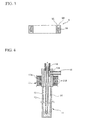
- the exothermic ring 9 has overall shape of a ring as shown in FIGS. 2 and 3 , and comprising an conductive member 9A comprising carbon, and a quartz-coated member 9B which covers the conductive member 9A with an interval of space therebetween.
- This internal space 9C that is surrounded by the quartz-coated member 9B is evacuated to create a vacuum state on the order of 10 -4 ⁇ 10 -6 Pa.
- This exothermic ring 9 is held horizontally at a position above the high-frequency induction heating coil 8 by a support member 11 which hangs downward from the top wall 1A of the housing 1.
- This support member 11 is formed in the shape of the letter L by a vertical part 11A and a horizontal part 11B.
- the top end of the vertical part 11A passes through the top wall 1 A of the housing 1 and is supported on top wall 1A to permit rotation, raising and lowering.
- the exothermic ring 9 is fixed in place to the front end of the horizontal part 11B which is combined with the bottom end of the vertical part 11A.
- An operating device 11C such as a lever or the like, is provided at the top end of the vertical part 11A which projects out from the top wall 1A of the housing 1.
- the exothermic ring 9 held at the bottom end thereof can be moved slightly up or down, and can be subjected to reciprocating movement between a "heating position” (the position indicated by the symbol E in FIG. 2 ), which is disposed to the space between the polycrystal holder 5 and the seed crystal holder 7, and a "stand-by position" (the position indicated by the symbol F in the same figure) which is removed laterally from this space.
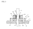
- At least the vertical part 11A of the support member 11 is provided with a double tube structure comprising an outer tube 12 and an inner tube 13 such as shown in FIG. 4 , with a cooling flow path 14 formed in the space of the double tube.
- the bottom end of the outer tube 12 is sealed, but the bottom end of the inner tube 13 is open and is disposed at a position that is slightly distant from the bottom end of the outer tube 12.
- an external tube 15 for supplying a cooling medium such as cooled water from the outside is connected to an attachment hole 12A at the top of the outer tube 12, and an external tube 16 for expelling a cooling medium is connected at the top end of the inner tube 13.
- the cooling flow path 14 formed by the double tube is designed so that the cooling medium which is supplied from the external pipe 15 to the ring-shaped space between the outer tube 12 and the inner tube 13 is returned at the bottom end of the support member 11, passes through the inside of the inner tube 13, and is expelled to the outside from the external tube 16. The entirety of the support member 11 is thus cooled as a result of this type of circulation of the cooling medium.
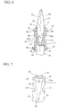
- the top end of the support member 11 is supported by a support block 17 that is provided so as to form a portion of the top wall 1A of the housing 1, as shown in FIG 5 .
- This support block 17 comprising a first block member 17A that is fixed in place to the upper surface of the top wall 1A of the housing 1, and a second block member 17B that is fixed in place on top of the first block member 17A.
- the support member 11 is disposed so as to pass through these block members 17A, 17B and the top wall 1A of the housing 1 in the vertical direction.
- a sleeve 18 is provided in a unitary manner with the block members 17A and 17B so as to form a penetrating hole in the block members 17A, 17B.
- the support member 11 is supported penetrating through the penetrating hole 18a of the sleeve 18, and passes thorough the holes 19,20 of the block member 17A and the top wall 1A of the housing 1, so as to be suspended within the housing 1.
- Sealing members 21A-21C are provided in between the support member 11 and the inner peripheral surface of the penetrating hole 18a of the sleeve 18, in between the upper surface of the top wall 1A of the housing 1 and the bottom surface of the first block member 17A of the support block 17, and in between the sleeve 18 and the second block member 17B, for maintaining hermetic within the housing 1.
- the numeric symbol 22 indicates a screw that fixes the first block member 17A and the top wall 1A of the housing 1 in place in a unitary manner.
- the seed crystal holder 7 is formed of tantalum (Ta) and has the overall shape of a cylinder such as shown in FIGS. 6 and 7 .
- a conical upper housing aperture 32 is formed to the majority of the seed crystal holder 7, excluding the bottom end thereof, this conical upper housing aperture having a gradually widening diameter as it approaches the opening 31 at the top end of the seed crystal holder 7.
- a cylindrical lower housing aperture 33 is formed to the bottom end of the seed crystal holder 7.
- the seed crystal 6 which is held by the seed crystal holder 7 is formed so that its overall shape is that of a rod, it is formed to be conical in shape, such that it narrows along the direction of its length from its center toward the respective ends, top end 6a and bottom portion 6b.
- the support member 34 is formed to be cylindrical in shape.
- the seed crystal holder 7 is attached on top of the support member 34, and the bottom end 6b of the seed crystal 6 is housed in the upper housing aperture 32.
- the axial line C 2 of the seed crystal 6 is disposed so as to be on the same line as the axial line C 3 of the polycrystalline silicon rod S1 which is held by polycrystal holder 5 above.
- screw holes 35 extending in the radial direction are provided at 90° intervals along the circumferential direction at either end of the seed crystal holder 7. These screw holes 35 each pass through the wall of the seed crystal holder 7, and thereby communicate with the internal upper housing aperture 32 and lower housing aperture 33.
- the seed crystal 6 housed inside the upper housing aperture 32 is fixed in place by screwing into place set screws 36 via the upper screw holes 35.
- the support member 34 housed in the lower housing aperture 33 is fixed in place by screwing into place set screws 36 via lower screw holes 35.
- a tapered surface 32a is formed to the inner peripheral surface of the upper housing aperture 32 of the seed crystal holder 7, and the angle ⁇ which this tapered surface 32a forms with the axial line C 1 of the upper housing aperture 32 is set to be in the range of 10 ⁇ 25°.
- the surface roughness of this tapered surface 32a is set to have an average roughness (Ra) in the range of 10 ⁇ 200 ⁇ m.
- Ra average roughness
- the angle of the tapered surface 32a is more preferably set to be in the range of 17 ⁇ 18°. Further, by setting the surface roughness to be in the range of 10 ⁇ 200 ⁇ m, the seed crystal 6 can be held with an appropriate frictional force during rotation, so that its position can be accurately maintained.
- Respective concavities 37 are formed to the outer periphery of the seed crystal holder 7 at the center position along its length, these concavities 37 being formed at symmetrical positions separated 180° from one another in the circumferential direction. These concavities 37 are for disposing the front end of a pair of pliers or other such tool used when fixing the seed holder 7 in place to the support member 34, holding the seed crystal 6 inside the housing aperture 32, etc.
- the concavities 37 are formed to be a rectangular-shaped groove in cross-section, and are provided with a flat surface 37a parallel to the axis direction for enabling contact with the front end portion of a tool.
- the seed crystal 6, which has a conical shape at either portion 6a, 6b, is inserted into the upper housing aperture 32 of the seed crystal holder 7.
- the conically shaped outer peripheral surface of the seed crystal 6 comes into contact over its entire periphery with the tapered surface 32a of the housing aperture 32.
- both axial lines C 1 ,C 2 are correctly aligned.
- the axial line C 2 of the seed crystal 6 and the axial line C 3 of the polycrystalline silicon rod which is disposed above are correctly aligned.
- the seed crystal 6 is housed with the axial lines C 1 ,C 2 in a state of alignment, and the axial line C 3 of the polycrystalline silicon rod S 1 above is also aligned.
- the time of work for attaching the seed crystal 6 is greatly reduced.
- the seed crystal 6 is held over its entire periphery by the tapered surface 32a and can be fixed in place with certainty by further pressing force by the set screws 36.
- the upper housing aperture is straight, the seed crystal readily moves left and right within the clearance in the case where the seed crystal is housed and then stopped by the set screws.
- the housing aperture a tapered surface, the entire periphery of the seed crystal is in contact with the tapered surface, so that movement to the left or right is difficult. Accordingly, the operation of aligning the core with the polycrystalline silicon rod is facilitated.
- the polycrystalline silicon rod S1 is supported by the polycrystal holder 7 so as to have the same axis as the seed crystal 6.
- the exothermic ring 9 is disposed to the "heating position E" between the polycrystal holder 5 and the seed crystal holder 7 as shown in FIG. 1 .
- This exothermic ring 9 is subjected to induction heating by the high-frequency induction heating coil 8, to reach a high temperature state.
- the polycrystalline silicon rod S1 is heated by the radiant heat from the exothermic ring 9. Further, the temperature of the polycrystalline silicon rod S1 raises and the bottom end thereof becomes glowing.
- the support member 11 is rotated and the exothermic ring 9 is receded from between the polycrystal holder 5 and the seed crystal holder 7, to the "stand-by position F".
- the polycrystalline silicon rod S1 is heated only by induction heating from the high-frequency induction heating coil 8, to grow the single crystal silicon. Because the exothermic ring 9 is covered with quartz, contamination from the ring member is extremely small, making it possible to produce extremely high quality single crystal silicon.
- the seed crystal 6 is rotated during the process of growing the single crystal silicon. However, since the entire periphery of the seed crystal 6 is held by the tapered surface 32a of the housing aperture 22 during this time, slipping does not occur and the state of core alignment can be maintained.
- the roughness of the tapered surface is set to be in the range of an average roughness (Ra) of 10 ⁇ 200 ⁇ m.
- Ra average roughness
- the cooling medium flows through the cooling flow path 14 inside the support member 11 which is in the form of a double tube.
- the exothermic ring 9 is heated by the high-frequency induction heating coil 8, that heat is prevented from reaching the sealing member 21A which seals the space between the support member 11 and the housing 1.
- contamination from the support member 11 is prevented.
- the sealing member 21A does not become overheated, so that a deterioration in the sealing member 21A and a decline in its performance can be prevented.
- contamination from the sealing member 21A is prevented and an extension in the useful life of the sealing member 2 1 A can be anticipated.
- the conductive member 9A consisting of carbon is covered by the quartz-coated member 9B, it is possible to prevent contamination of the work environment.
- the heat effect on the polycrystalline silicon rod S 1 is high and deterioration in the conductive member caused by a residual moisture component in the case of an air environment can be prevented.
- the conductive member 9A and the quartz-coated member 9B it is possible to prevent the generation of stress that accompanies the difference in thermal expansion between these two elements..
- the support member 11 is formed of a double tube consisting of an inner tube 12 and an outer tube 13.
- a cooling medium is supplied to one of either the inner tube 12 or the outer tube 13, with this cooling medium then passing through the other tube to be expelled. Because of this design, it is possible to continuously supply the cooling medium to the support member 11, so that the sealing member can be effectively cooled. Due to these synergistic effects, the soundness of the apparatus for producing single crystal silicon can be maintained over a long period of time.
- FIG. 8 shows another embodiment of the present invention.
- the exothermic ring 41 differs from the exothermic ring 9 of the first embodiment shown in FIGS. 1 ⁇ 3 in that a cutout 42 is formed to part of the periphery
- the space interval W of this cutout 42 is formed to be larger than the diameter of the polycrystalline silicon rod S1, so that the polycrystalline silicon rode S 1 can pass through the cutout 42.
- the position of the cutout 42 is disposed so that, when the operating lever 11C is manipulated to cause reciprocating movement of the exothermic ring 41, the polycrystalline silicon rod S1 passes through the cutout 42 when the exothermic ring 41 is moved between the heating position E (equivalent to the center of the support for the polycrystal holder 5 and the axial line C 1 of the seed crystal holder 7) and the stand-by position F by the operating device. Accordingly, in the production step (6) in the first embodiment above, the polycrystalline silicon rod S 1 is raised and moved away from the seed crystal 6 prior to moving the exothermic ring 9 from the heating position E to the stand-by position F.
- an operating device such as a lever was provided for rotating, raising or lowering the support member 11.
- an operating device consisting of a driving mechanism that incorporates an electric motor or a speed reducer.
- carbon, molybdem or the like may be suitably employed for the conductive member of the exothermic ring, provided that the conductive member is one which can undergo induced heating by an induction heating coil and which has a higher melting point than that of silicon.
- the upper housing aperture 32 is formed with a tapered surface 32a which is continuous to the opening.
- the vicinity of the opening can be in the form of a cylinder.
- the seed crystal inserted into the housing aperture was fixed in place with four set screws, however, it is also acceptable to fix the seed crystal in place using three set screws.
Landscapes
- Chemical & Material Sciences (AREA)
- Engineering & Computer Science (AREA)
- Crystallography & Structural Chemistry (AREA)
- Materials Engineering (AREA)
- Metallurgy (AREA)
- Organic Chemistry (AREA)
- Crystals, And After-Treatments Of Crystals (AREA)
Applications Claiming Priority (1)
| Application Number | Priority Date | Filing Date | Title |
|---|---|---|---|
| JP2007331548 | 2007-12-25 |
Publications (3)
| Publication Number | Publication Date |
|---|---|
| EP2075357A2 true EP2075357A2 (de) | 2009-07-01 |
| EP2075357A3 EP2075357A3 (de) | 2010-03-31 |
| EP2075357B1 EP2075357B1 (de) | 2016-07-27 |
Family
ID=40386409
Family Applications (1)
| Application Number | Title | Priority Date | Filing Date |
|---|---|---|---|
| EP08172934.5A Ceased EP2075357B1 (de) | 2007-12-25 | 2008-12-24 | Vorrichtung zur Herstellung von Einkristall-Silizium |
Country Status (5)
| Country | Link |
|---|---|
| US (1) | US8313577B2 (de) |
| EP (1) | EP2075357B1 (de) |
| JP (2) | JP5157878B2 (de) |
| KR (1) | KR101485188B1 (de) |
| CN (1) | CN101469444B (de) |
Families Citing this family (11)
| Publication number | Priority date | Publication date | Assignee | Title |
|---|---|---|---|---|
| US8444800B2 (en) * | 2009-10-29 | 2013-05-21 | Mitsubishi Materials Corporation | Apparatus and method of manufacturing silicon seed rod |
| CN102140686A (zh) * | 2010-02-03 | 2011-08-03 | 中国科学院福建物质结构研究所 | 一种新型的多晶硅熔炼炉 |
| DE102011080866A1 (de) * | 2011-08-12 | 2013-02-14 | Wacker Chemie Ag | Verfahren zur Herstellung eines einkristallinen Stabes aus Silicium |
| US9410263B2 (en) * | 2013-03-15 | 2016-08-09 | Mitsubishi Polycrystalline Silicon America Corporation (MIPSA) | FZ seed holder and pre-heater |
| CN105002556A (zh) * | 2014-04-21 | 2015-10-28 | 洛阳金诺机械工程有限公司 | 一种拉制硅芯时提高硅芯结晶速度的装置 |
| CN106498495B (zh) * | 2016-11-02 | 2018-09-11 | 中国电子科技集团公司第四十六研究所 | 一种真空区熔硅单晶生长用加热线圈的表面预处理方法 |
| CN107513760A (zh) * | 2017-09-04 | 2017-12-26 | 青海鑫诺光电科技有限公司 | 一种单晶棒放肩装置及其使用方法 |
| CN107366017A (zh) * | 2017-09-04 | 2017-11-21 | 青海鑫诺光电科技有限公司 | 一种单晶硅收尾设备及其使用方法 |
| CN108546987B (zh) * | 2018-07-26 | 2019-08-06 | 江苏金晖光伏有限公司 | 提纯太阳能级多晶硅的方法 |
| JP7637544B2 (ja) * | 2021-03-25 | 2025-02-28 | Tdk株式会社 | 結晶製造方法、結晶製造装置、及び単結晶 |
| CN113668045A (zh) * | 2021-08-24 | 2021-11-19 | 包头美科硅能源有限公司 | 一种颗粒硅直接用于区熔法制备单晶硅的装置及方法 |
Citations (2)
| Publication number | Priority date | Publication date | Assignee | Title |
|---|---|---|---|---|
| JPH0710681A (ja) | 1993-05-11 | 1995-01-13 | Hemlock Semiconductor Corp | 浮融帯装置用サセプタ |
| JP2007331548A (ja) | 2006-06-14 | 2007-12-27 | Toyota Motor Corp | 駐車支援装置 |
Family Cites Families (10)
| Publication number | Priority date | Publication date | Assignee | Title |
|---|---|---|---|---|
| US3935059A (en) * | 1969-07-21 | 1976-01-27 | U.S. Philips Corporation | Method of producing single crystals of semiconductor material by floating-zone melting |
| US3620682A (en) * | 1969-10-31 | 1971-11-16 | Siemens Ag | Apparatus for producing rod-shaped members of crystalline material |
| DE2533858C2 (de) * | 1975-07-29 | 1983-11-17 | Siemens AG, 1000 Berlin und 8000 München | Vorrichtung zum tiegelfreien Zonenschmelzen eines Halbleitermaterialstabes mit in axialer Richtung feststehender Induktionsheizspule |
| DE2557186A1 (de) * | 1975-12-18 | 1977-06-23 | Siemens Ag | Verfahren und vorrichtung zum herstellen von halbleitermaterialstaeben, insbesondere von siliciumstaeben mit grossen durchmessern, durch tiegelfreies zonenschmelzen |
| US4499354A (en) * | 1982-10-06 | 1985-02-12 | General Instrument Corp. | Susceptor for radiant absorption heater system |
| JPH02229791A (ja) * | 1989-03-03 | 1990-09-12 | Furukawa Electric Co Ltd:The | 化合物半導体単結晶製造装置 |
| JP2922078B2 (ja) * | 1993-03-17 | 1999-07-19 | 株式会社トクヤマ | シリコンロッドの製造方法 |
| JP2874722B2 (ja) * | 1993-06-18 | 1999-03-24 | 信越半導体株式会社 | シリコン単結晶の成長方法及び装置 |
| JPH11304791A (ja) * | 1998-04-24 | 1999-11-05 | Tokuyama Corp | 多結晶シリコンの不純物分析方法 |
| EP1806437B1 (de) * | 2004-09-03 | 2016-08-17 | Nippon Steel & Sumitomo Metal Corporation | Verfahren zur herstellung von siliciumcarbid-einkristall |
-
2008
- 2008-12-19 JP JP2008323584A patent/JP5157878B2/ja not_active Expired - Fee Related
- 2008-12-22 KR KR20080130852A patent/KR101485188B1/ko not_active Expired - Fee Related
- 2008-12-23 CN CN2008101849477A patent/CN101469444B/zh not_active Expired - Fee Related
- 2008-12-24 EP EP08172934.5A patent/EP2075357B1/de not_active Ceased
- 2008-12-24 US US12/343,798 patent/US8313577B2/en not_active Expired - Fee Related
-
2012
- 2012-10-19 JP JP2012232090A patent/JP5482859B2/ja not_active Expired - Fee Related
Patent Citations (2)
| Publication number | Priority date | Publication date | Assignee | Title |
|---|---|---|---|---|
| JPH0710681A (ja) | 1993-05-11 | 1995-01-13 | Hemlock Semiconductor Corp | 浮融帯装置用サセプタ |
| JP2007331548A (ja) | 2006-06-14 | 2007-12-27 | Toyota Motor Corp | 駐車支援装置 |
Also Published As
| Publication number | Publication date |
|---|---|
| KR20090069230A (ko) | 2009-06-30 |
| US20090158996A1 (en) | 2009-06-25 |
| US8313577B2 (en) | 2012-11-20 |
| JP5482859B2 (ja) | 2014-05-07 |
| CN101469444B (zh) | 2012-10-31 |
| JP2013010691A (ja) | 2013-01-17 |
| EP2075357A3 (de) | 2010-03-31 |
| CN101469444A (zh) | 2009-07-01 |
| EP2075357B1 (de) | 2016-07-27 |
| KR101485188B1 (ko) | 2015-01-22 |
| JP5157878B2 (ja) | 2013-03-06 |
| JP2009173530A (ja) | 2009-08-06 |
Similar Documents
| Publication | Publication Date | Title |
|---|---|---|
| US8313577B2 (en) | Apparatus for producing single crystal silicon | |
| CN102162123B (zh) | 双加热器移动热屏式直拉单晶炉 | |
| TWI730594B (zh) | 一種半導體晶體生長裝置 | |
| JPH1192272A (ja) | 単結晶製造装置および単結晶の製造方法 | |
| KR102777050B1 (ko) | 단결정 제조장치 | |
| JP2022518858A5 (de) | ||
| JP5270996B2 (ja) | シリコン単結晶引上装置 | |
| JP7101224B2 (ja) | 半導体結晶成長装置 | |
| JP2021066652A (ja) | 半導体結晶成長装置 | |
| CN118272909A (zh) | 一种晶体生长设备 | |
| JP2705809B2 (ja) | 単結晶引上装置 | |
| US20050066690A1 (en) | Method of and apparatus for producing optical fiber | |
| JP2006206351A (ja) | 引下げ装置及び当該装置に用いられる容器 | |
| CN103266346B (zh) | 一种引上法生长yvo4晶体的生长设备及基于该生长设备的生长方法 | |
| JPH06211589A (ja) | 半導体単結晶棒製造装置 | |
| JP4894749B2 (ja) | 単結晶シリコン製造装置 | |
| WO2022123957A1 (ja) | 単結晶製造装置 | |
| CN114232078A (zh) | 一种单晶炉的铱坩埚加热装置和单晶生长的方法 | |
| CN121610887B (zh) | 一种动态调节晶体生长过程中轴向温度梯度的装置及方法 | |
| JP4191704B2 (ja) | 引下げ装置 | |
| CN115417584B (zh) | 一种ct球管的制造工艺 | |
| CN121610887A (zh) | 一种动态调节晶体生长过程中轴向温度梯度的装置及方法 | |
| CN118639331A (zh) | SiC长晶装置及方法 | |
| CN119640383A (zh) | Tssg法生长大尺寸晶体的设备和方法 | |
| CN118390160A (zh) | 顶部和上部保温结构、单晶热场装置及方法 |
Legal Events
| Date | Code | Title | Description |
|---|---|---|---|
| PUAI | Public reference made under article 153(3) epc to a published international application that has entered the european phase |
Free format text: ORIGINAL CODE: 0009012 |
|
| AK | Designated contracting states |
Kind code of ref document: A2 Designated state(s): AT BE BG CH CY CZ DE DK EE ES FI FR GB GR HR HU IE IS IT LI LT LU LV MC MT NL NO PL PT RO SE SI SK TR |
|
| AX | Request for extension of the european patent |
Extension state: AL BA MK RS |
|
| PUAL | Search report despatched |
Free format text: ORIGINAL CODE: 0009013 |
|
| AK | Designated contracting states |
Kind code of ref document: A3 Designated state(s): AT BE BG CH CY CZ DE DK EE ES FI FR GB GR HR HU IE IS IT LI LT LU LV MC MT NL NO PL PT RO SE SI SK TR |
|
| AX | Request for extension of the european patent |
Extension state: AL BA MK RS |
|
| 17P | Request for examination filed |
Effective date: 20100929 |
|
| AKX | Designation fees paid |
Designated state(s): DE IT |
|
| GRAP | Despatch of communication of intention to grant a patent |
Free format text: ORIGINAL CODE: EPIDOSNIGR1 |
|
| RIC1 | Information provided on ipc code assigned before grant |
Ipc: C30B 13/20 20060101ALI20160302BHEP Ipc: C30B 29/06 20060101AFI20160302BHEP Ipc: C30B 13/32 20060101ALI20160302BHEP Ipc: C30B 13/00 20060101ALI20160302BHEP |
|
| INTG | Intention to grant announced |
Effective date: 20160324 |
|
| GRAS | Grant fee paid |
Free format text: ORIGINAL CODE: EPIDOSNIGR3 |
|
| GRAA | (expected) grant |
Free format text: ORIGINAL CODE: 0009210 |
|
| AK | Designated contracting states |
Kind code of ref document: B1 Designated state(s): DE IT |
|
| REG | Reference to a national code |
Ref country code: DE Ref legal event code: R096 Ref document number: 602008045290 Country of ref document: DE |
|
| PG25 | Lapsed in a contracting state [announced via postgrant information from national office to epo] |
Ref country code: IT Free format text: LAPSE BECAUSE OF FAILURE TO SUBMIT A TRANSLATION OF THE DESCRIPTION OR TO PAY THE FEE WITHIN THE PRESCRIBED TIME-LIMIT Effective date: 20160727 |
|
| REG | Reference to a national code |
Ref country code: DE Ref legal event code: R097 Ref document number: 602008045290 Country of ref document: DE |
|
| PLBE | No opposition filed within time limit |
Free format text: ORIGINAL CODE: 0009261 |
|
| STAA | Information on the status of an ep patent application or granted ep patent |
Free format text: STATUS: NO OPPOSITION FILED WITHIN TIME LIMIT |
|
| 26N | No opposition filed |
Effective date: 20170502 |
|
| PGFP | Annual fee paid to national office [announced via postgrant information from national office to epo] |
Ref country code: DE Payment date: 20221213 Year of fee payment: 15 |
|
| REG | Reference to a national code |
Ref country code: DE Ref legal event code: R081 Ref document number: 602008045290 Country of ref document: DE Owner name: HIGH-PURITY SILICON CORP., YOKKAICHI-SHI, JP Free format text: FORMER OWNER: MITSUBISHI MATERIALS CORP., TOKYO, JP |
|
| REG | Reference to a national code |
Ref country code: DE Ref legal event code: R119 Ref document number: 602008045290 Country of ref document: DE |
|
| PG25 | Lapsed in a contracting state [announced via postgrant information from national office to epo] |
Ref country code: DE Free format text: LAPSE BECAUSE OF NON-PAYMENT OF DUE FEES Effective date: 20240702 |
|
| PG25 | Lapsed in a contracting state [announced via postgrant information from national office to epo] |
Ref country code: DE Free format text: LAPSE BECAUSE OF NON-PAYMENT OF DUE FEES Effective date: 20240702 |