EP2066035B1 - Oscillation frequency control circuit - Google Patents
Oscillation frequency control circuit Download PDFInfo
- Publication number
- EP2066035B1 EP2066035B1 EP07830943A EP07830943A EP2066035B1 EP 2066035 B1 EP2066035 B1 EP 2066035B1 EP 07830943 A EP07830943 A EP 07830943A EP 07830943 A EP07830943 A EP 07830943A EP 2066035 B1 EP2066035 B1 EP 2066035B1
- Authority
- EP
- European Patent Office
- Prior art keywords
- voltage
- pulse generation
- output
- information
- control voltage
- Prior art date
- Legal status (The legal status is an assumption and is not a legal conclusion. Google has not performed a legal analysis and makes no representation as to the accuracy of the status listed.)
- Active
Links
Images


Classifications
-
- H—ELECTRICITY
- H03—ELECTRONIC CIRCUITRY
- H03L—AUTOMATIC CONTROL, STARTING, SYNCHRONISATION OR STABILISATION OF GENERATORS OF ELECTRONIC OSCILLATIONS OR PULSES
- H03L7/00—Automatic control of frequency or phase; Synchronisation
- H03L7/06—Automatic control of frequency or phase; Synchronisation using a reference signal applied to a frequency- or phase-locked loop
- H03L7/08—Details of the phase-locked loop
- H03L7/14—Details of the phase-locked loop for assuring constant frequency when supply or correction voltages fail
-
- H—ELECTRICITY
- H03—ELECTRONIC CIRCUITRY
- H03L—AUTOMATIC CONTROL, STARTING, SYNCHRONISATION OR STABILISATION OF GENERATORS OF ELECTRONIC OSCILLATIONS OR PULSES
- H03L7/00—Automatic control of frequency or phase; Synchronisation
- H03L7/06—Automatic control of frequency or phase; Synchronisation using a reference signal applied to a frequency- or phase-locked loop
- H03L7/08—Details of the phase-locked loop
- H03L7/085—Details of the phase-locked loop concerning mainly the frequency- or phase-detection arrangement including the filtering or amplification of its output signal
- H03L7/095—Details of the phase-locked loop concerning mainly the frequency- or phase-detection arrangement including the filtering or amplification of its output signal using a lock detector
-
- H—ELECTRICITY
- H03—ELECTRONIC CIRCUITRY
- H03L—AUTOMATIC CONTROL, STARTING, SYNCHRONISATION OR STABILISATION OF GENERATORS OF ELECTRONIC OSCILLATIONS OR PULSES
- H03L7/00—Automatic control of frequency or phase; Synchronisation
- H03L7/06—Automatic control of frequency or phase; Synchronisation using a reference signal applied to a frequency- or phase-locked loop
- H03L7/08—Details of the phase-locked loop
- H03L7/085—Details of the phase-locked loop concerning mainly the frequency- or phase-detection arrangement including the filtering or amplification of its output signal
- H03L7/093—Details of the phase-locked loop concerning mainly the frequency- or phase-detection arrangement including the filtering or amplification of its output signal using special filtering or amplification characteristics in the loop
-
- H—ELECTRICITY
- H03—ELECTRONIC CIRCUITRY
- H03L—AUTOMATIC CONTROL, STARTING, SYNCHRONISATION OR STABILISATION OF GENERATORS OF ELECTRONIC OSCILLATIONS OR PULSES
- H03L7/00—Automatic control of frequency or phase; Synchronisation
- H03L7/06—Automatic control of frequency or phase; Synchronisation using a reference signal applied to a frequency- or phase-locked loop
- H03L7/08—Details of the phase-locked loop
- H03L7/14—Details of the phase-locked loop for assuring constant frequency when supply or correction voltages fail
- H03L7/146—Details of the phase-locked loop for assuring constant frequency when supply or correction voltages fail by using digital means for generating the oscillator control signal
Definitions
- the present invention relates to an oscillation frequency control circuit according to the preamble of claim 1 and 2, and more particularly, to an oscillation frequency control circuit capable of correcting its own frequency in synchronism with an output signal and maintaining a stable oscillation frequency even when a highly stable reference signal is not input thereto.
- An oscillation frequency control circuit according to the preamble of claims 1 and 2 is disclosed in US 6,313,708 B1 .
- a reference timing signal apparatus including an oscillator with phase-locked loop which provides a clock signal in a CDMA base station is disclosed in US 7,015,762 B1 .
- US 5,335,364 A describes a circuit arrangement by which a voltage-controlled temperature-compensated oscillator serving as the frequency reference in a radio telephone is controlled.
- a cesium frequency reference oscillator, a rubidium frequency reference oscillator, a reference oscillator of a frequency synchronization type using a GPS signal, and the liker are used in broadcasting and communication systems.
- the reference signal from the oscillators is divided to be used as a reference signal source of an apparatus.
- the divided reference signal is used as a reference clock for a communication system.
- the reference signal is used as a reference signal for phase comparison in a PLL (phase locked loop) circuit, a reference clock signal for a DSP (digital signal processor), an FPGA (field programmable gate array) or the like, and a sampling clock for a D/A (digital/analog) converter or an A/D (analog/digital) converter.
- PLL phase locked loop
- DSP digital signal processor
- FPGA field programmable gate array
- Fig. 6 is a configuration block diagram of a typical PLL circuit.
- the PLL circuit is provided with a phase comparator 32 configured to compare an external reference signal (Fref) with a 1/N divided signal to output a phase difference signal, a charge pump 33 configured to output the phase difference as a pulse width signal, a loop filter 34 configured to smooth out an output voltage from the charge pump 33, a voltage controlled crystal oscillator (VCXO) 35 configured to change a frequency in accordance with a control voltage from the loop filter 34 to oscillate and output a desired frequency (internal reference signal: output frequency), and a frequency divider (divider) 36 configured to divide the output (internal reference signal) of the VCXO 35 to 1/N.
- the internal reference signal corresponds to an N*Fref signal.
- the PLL circuit is configured to apply feedback control to the internal VCXO 35 so that a phase difference between an external reference signal and the output frequency of the VCXO 35 to thereby obtain an oscillator output synchronized with the reference signal.
- the phase comparator 32 is configured to compare phases of a highly stable external reference signal and an output signal from the VCXO 35 performing frequency control based on an input voltage and perform PLL control so that a DC voltage obtained by smoothing out a phase comparison result is fed back to the VCXO 35 to thereby generating a highly precise signal.
- the PLL circuit is widely used in communication and broadcasting apparatuses and the like.
- Patent Document 1 Japanese Patent Application Laid-Open No. 2000-083003
- Patent Document 2 Japanese Patent Application Laid-Open No. 2003-179489
- Patent Document 1 discloses a free running frequency adjustment system in which a frequency counter performs a counting operation synchronized with an output signal of a VCO (voltage controlled oscillator) which is input within a period of time corresponding to a pulse width, a latch circuit stores therein a count value corresponding to an oscillation frequency of the VCO, and when the count value deviates from a predetermined range, a CPU changes an application voltage to the VCO to adjust a free-running frequency of the VCO 10 to be within a predetermined range.
- VCO voltage controlled oscillator
- Patent Document 2 discloses a phase locked loop circuit having a function of automatically adjusting a free-running frequency of a voltage-controlled oscillator (VCO), in which a microcomputer counts the number of pulses of a pulse signal output from the VCO in a period in which an output from a phase comparator is at a predetermined level and updates a control data based on the counted value, and a DAC (digital analog converter) converts the data to an analog signal so that the analog signal is combined with a signal from an LPF (low pass filter) to be used as a frequency control signal of the VCO.
- VCO voltage-controlled oscillator
- the PLL circuit since the phase comparison cannot be performed when a reference signal is not input thereto, the PLL circuit may switch over to another external reference signal or operate in a free-running state of the voltage-controlled oscillator. When it switches over to another external reference signal from a backup system, since PLL control is performed again, the deviation of the reference signal depends on the external reference signal, and therefore, it does not cause any problem. However, when it switches over to operate in the free-running state, the frequency is excessively controlled in response to a phase comparison result during the switching to stick to an upper or lower limit frequency, and thus, there is a problem that the frequency deviation becomes large.
- VC-TCXO voltage controlled-temperature compensated crystal oscillator
- a frequency deviation may amount to maximum 10.5 ppm at the elapse of 10 years. This may also be explained that if an output frequency of a carrier wave in communication is 800 MHz, a frequency deviation may amount to 8.4 kHz similar to that of the reference frequency. Such a frequency deviation is not allowable to a system.
- the system or circuit disclosed in Patent Document 1 or 2 counts the output of the VCO or the output of the phase comparator to perform adjustment of the free-running frequency.
- the system or circuit does not perform the frequency adjustment by directly detecting an abnormality of the external reference signal and is unable to sufficiently cope with the aging.
- Fig. 7 is a view showing exemplary control voltage characteristics of a voltage controlled crystal oscillator.
- the horizontal axis represents a control voltage
- the vertical axis represents a frequency deviation.
- the VCXO is able to operate when the control voltage is in the range of 0 to 4 V, while it is unable to operate when the control voltage is 4 V or more. Since the frequency deviation rises with the lapse of time even in the case of the VCXO, an appropriate control voltage changes accordingly.
- the present invention has been made in consideration of the aforementioned situation, and it is an object of the invention to provide an oscillation frequency control circuit capable of correcting its own frequency and maintaining a stable oscillation frequency even when a highly stable reference signal is not input thereto and it operates is in a free-running state.
- the present invention provides an oscillation frequency control circuit according to claims 1 and 2. Preferred embodiments are defined in the dependent claims.
- an oscillation frequency control circuit comprising: a voltage-controlled oscillator; a frequency divider configured to divide an output from the voltage-controlled oscillator; a phase comparator configured to compare phases of an external reference signal and an output from the frequency divider; a loop filter configured to smooth out an output from the phase comparator and output the smoothed output; a detection circuit capable of detecting the external reference signal; a pulse generation circuit configured to generate pulses upon receipt of a pulse generation information to be output to the loop filter; a memory capable of storing therein a prescribed voltage information and the pulse generation information corresponding to the prescribed voltage information; a switch configured to turn on/off a connection between the phase comparator and the loop filter; and a control unit configured to turn on the switch when a level of the external reference signal detected by the detection circuit is within an appropriate range while turning off the switch when the level is outside the appropriate range to thereby output the pulse generation information stored in the memory to the pulse generation circuit.
- the memory stores an aging characteristics table, the table storing a control voltage appropriate for an aging time and a pulse generation information corresponding to the control voltage, and the control unit measures time by means of a timer provided therein, retrieves the control voltage corresponding to the measured time from the aging characteristics table of the memory when the level of the external reference signal is outside the appropriate range, reads out the pulse generation information corresponding to the retrieved control voltage, and output the read pulse generation information to the pulse generation circuit.
- a level detection circuit configured to detect a voltage level of an output from the loop filter to thereby output a latest voltage information to the control unit
- the memory stores a voltage/pulse generation information table the table storing the latest voltage information, a plurality of voltage information, and a pulse generation information corresponding to the voltage information
- the control unit updates the latest voltage information of the memory to the latest voltage information input from the level detection circuit, reads out the pulse generation information corresponding to the latest voltage information from the voltage/pulse generation information table of the memory when the level of the external reference signal is within the appropriate range, and output the read pulse generation information to the pulse generation circuit.
- a voltage controlled crystal oscillator In the oscillation frequency control circuit according to the above aspect of the present invention, a voltage controlled crystal oscillator, a voltage controlled-temperature compensated crystal oscillator, or a voltage controlled, oven controlled crystal oscillator is used in lieu of the voltage-controlled oscillator.
- the pulse generation circuit is a pulse width modulation circuit
- the pulse generation information output from the control unit is information on a pulse width modulation duty cycle
- a stable oscillation frequency can be maintained by succeeding the previous operation state even when the reference signal is not input and it operates in a free-running state.
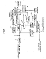
- Fig. 1 is a configuration block diagram of an oscillation frequency control circuit according to an embodiment of the present invention.
- the oscillation frequency control circuit (present circuit) according to the embodiment of the present invention includes a filter 11, a phase comparator 12, a phase comparator 12, a switch 13, a loop filter 14, a voltage-controlled oscillator 15, a frequency divider 16, a detection circuit 17, an amplifier 18, a CPU (central processing unit) 20, a memory 21, a PWM (pulse width modulation) circuit 22, a level detection circuit 23, an AD converter 24, and an AD converter 25.
- a filter 11 includes a filter 11, a phase comparator 12, a phase comparator 12, a switch 13, a loop filter 14, a voltage-controlled oscillator 15, a frequency divider 16, a detection circuit 17, an amplifier 18, a CPU (central processing unit) 20, a memory 21, a PWM (pulse width modulation) circuit 22, a level detection circuit 23, an AD converter 24, and an AD converter 25.
- PWM pulse width modulation
- the filter 11 is a filter configured to limit a band of an external reference signal having a frequency of e.g., 10 MHz.
- the filter 11 has a function of rejecting a highfrequency component of the external reference signal, although the function is not essential as a basic configuration.
- the phase comparator 12 is configured to compare phases of a reference signal output from the filter 11 and a signal of which the frequency is divided by the frequency divider 16 to thereby output a phase difference signal. Moreover, the phase comparator 12 is configured to compares the phases of the external reference signal and the frequency-divided signal to thereby output a lock detection signal to the CPU 20 when a synchronization (lock) has been detected, while outputting an unlock detection signal to the CPU 20 when an asynchronism (unlock) has been detected.
- the switch 13 is configured to turn on/off a connection between the phase comparator 12 and the loop filter 14 in accordance with a switching command from the CPU 20. That is, upon receipt of a turn-on command from the CPU 20, the switch 13 supplies an output from the phase comparator 12 to the loop filter 14, while cutting off the connection between the phase comparator 12 and the loop filter 14 upon receipt of a turn-off command from the CPU 20.
- the loop filter 14 is a filter configured to smooth out an output voltage from the phase comparator 12: that is, the filter smoothes out a control voltage to be input to the voltage-controlled oscillator 15.
- the voltage-controlled oscillator 15 is configured to change a frequency in accordance with the control voltage from the loop filter 14 to oscillate and output a desired frequency (internal reference signal).
- a voltage controlled crystal oscillator (VCXO) or a voltage controlled, oven controlled crystal oscillator (VC-OCXO) may be used in lieu of the voltage-controlled oscillator (VCO).
- the frequency divider 16 is configured to divide the internal reference signal output from the voltage-controlled oscillator 15 to 1/N.
- the detection circuit 17 is configured to detect a level of the output signal from the filter 11.
- the amplifier 18 is configured to amplify a signal detected by the detection circuit 17.
- the CPU 20 is configured to receive a control voltage information from the AD converter 25 and store the control voltage information in the memory 21 as a latest control voltage information. Specifically, the CPU 20 always receives the control voltage information from the AD converter 25, and when the received control voltage information has not been changed from a previous control voltage information, the control voltage information stored in the memory 21 is not updated, while when the received control voltage information has been changed from the previous control voltage information, the control voltage information of the memory 21 is updated.
- the CPU 20 upon receipt of the detected level of the external reference signal (external REF) from the AD converter 24, the CPU 20 makes a determination as to whether the detected level is within an appropriate range (ranging from a first threshold value to a second threshold value) stored in the memory 21 and output a turn-on command to the switch 13 when it is within the appropriate range while outputting a turn-off command to the switch 13 when it is outside the appropriate range.
- an appropriate range ranging from a first threshold value to a second threshold value
- the CPU 20 refers to a voltage and PWM duty cycle table stored in the memory 21, and outputs a pulse width information corresponding to a PWM duty cycle based on a voltage information of a present (latest) control voltage to the PWM circuit 22.
- the memory 21 stores therein the latest control voltage information, the first and second threshold values serving as a basis of the appropriate range for the detection level of the external REF, and the voltage and PWM duty cycle table.
- the control voltage information is updated in the memory 21 when a change has been detected by the level detection circuit 23, so that a latest value can be maintained.
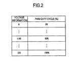
- Fig. 2 is a schematic view of the voltage and PWM duty cycle table. As shown in Fig. 2 , the voltage and PWM duty cycle table stores a PWM duty cycle (%) for specifying a pulse width for a voltage information.
- the voltage information is used to predetermine a PWM duty cycle of pulses output from the PWM circuit 22 to the loop filter 14 in order to maintain a value (control voltage information) of the control voltage from the loop filter 14. Therefore, when a PWM duty cycle corresponding to the control voltage information detected by the level detection circuit 23 is read from the voltage and PWM duty cycle table and the PWM circuit 22 outputs pulses corresponding to the cycle to the loop filter 14, the same control voltage as the previous one is output from the loop filter 14 to the voltage-controlled oscillator 15.
- the PWM circuit 22 performs pulse width modulation on data of the PWM duty cycle input from the CPU 20 to thereby output a desired pulse signal to the loop filter 14.
- the level detection circuit 23 is configured to detect a DC voltage output from the loop filter 14 to output the detected voltage to the AD converter 25 as the control voltage information.
- the AD converter 24 is configured to convert an analog signal of the detection level of the external REF output from the amplifier 18 to a digital signal to be output to the CPU 20.
- the AD converter 25 is also configured to convert an analog signal of the control voltage information from the level detection circuit 23 to a digital signal to be output to the CPU 20.
- the switch 13 is turned on and the phase comparator 12 and the loop filter 14 are in a connected state.
- the phase comparator 12 outputs the phase difference signal of the external reference signal and the signal from the frequency divider 16 to the voltage-controlled oscillator 15 via the loop filter 14 and controls an oscillation frequency of the voltage-controlled oscillator 15.
- the level detection circuit 23 detects a latest control voltage to output the latest control voltage to the CPU 20 via the AD converter 25, and the CPU 20 updates the latest control voltage information stored in the memory 21 when the control voltage information has been changed.
- the external reference signal is detected by the detection circuit 17 and amplified by the amplifier 18 so that the level of the external REF is detected and output to the CPU 20 via the AD converter 24.
- the CPU 20 When the determination result shows that the detection level is within the appropriate range, the CPU 20 operates in a normal state to maintain the turn-on state of the switch 13. When the determination result shows that the detection level is outside the appropriate range, the CPU 20 operates in an abnormal state to put the switch 13 in a turn-off state so that the connection between the phase comparator 12 and the loop filter 14 is out off.
- the CPU 20 reads out the latest control voltage information stored in the memory 21, reads the PWM duty cycle corresponding to the voltage information from the voltage and PWM duty cycle table, and outputs information (data) for forming pulses corresponding to the PWM duty cycle to the PWM circuit 22.
- the PWM circuit 22 generates pulses in accordance with the pulse generation information input from the CPU 20 and output the control voltage to the voltage-controlled oscillator 15 via the loop filter 14.
- the CPU 20 immediately detects the abnormality from the output from the detection circuit 17 in the amplifier 18 and cuts off the output of the phase comparator 12, so that the same pulses as the previous control voltage which has been used for controlling the voltage-controlled oscillator 15 can be output from the PWM circuit 22. That is, by utilizing the output from the PWM circuit 22 in lieu of the output from the phase comparator 12, it is possible to appropriately control the frequency oscillation at the voltage-controlled oscillator 15 by succeeding the previous operation state.
- a default voltage information may be stored so that the pulse generation information may be output based on the PWM duty cycle corresponding to the default voltage information.
- the memory 21 stores therein a center voltage value within the appropriate range, of the control voltage of the voltage-controlled oscillator 15. Since the PWM duty cycle corresponding to the center voltage value is 50%, if the control voltage of the voltage-controlled oscillator 14 ranges from 0 to 3.3 V, the center control voltage is set to 3.3/2 V. Moreover, an arbitrary voltage value other than the center voltage value may be stored so that a control voltage is set to a voltage corresponding to the voltage value. When a default voltage information is used, it is possible to omit components such as the level detection circuit 23 and the AD converter 25 and the voltage and PWM duty cycle table in the memory 21.
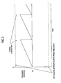
- Fig. 3 is a view showing characteristics during correction.
- the frequency deviation rises or falls.
- an appropriate reference signal is input at a specific timing, and when the inputting of the reference signal is stopped, the correction is made such that the frequency deviation returns to the center frequency by free-running control.
- Such corrections are repeated twice in Fig. 3 .
- the frequency control is carried out by using a center voltage value within a range capable of controlling the control voltage of the voltage-controlled oscillator 15.
- the correction operation can be performed without connecting a special circuit during the correction.
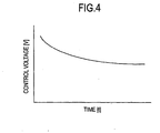
- Fig. 4 is a view showing aging and control voltage characteristics. As shown in Fig. 4 , in the present circuit, the optimum control voltage decreases with the elapse of time (however, this corresponds to a case where the frequency deviation is rising).
- Fig. 5 is a schematic view of an aging characteristics table. Although the memory 21 stores therein the voltage and PWM duty cycle table, the present circuit uses the aging characteristics table shown in Fig. 5 in lieu of the voltage and PWM duty cycle.
- the aging characteristics table of Fig. 5 incorporates a time factor into the relationship between the voltage information and the PWM duty cycle. Specifically, a voltage information which is appropriately set for a given elapse time and a PWM duty cycle corresponding to the voltage information are stored as a table. The CPU 20 measures an elapse time by means of a timer provided therein.
- the CPU 20 turns off the switch 13, refers to the time measured by the internal timer to retrieve the PWM duty cycle from the voltage information corresponding to the time, and outputs a pulse generation information corresponding to the PWM duty cycle to the PWM circuit 22. Then, the PWM circuit 22 generates desired pulses and outputs the control voltage to the voltage-controlled oscillator 15 via the loop filter 14.
- the CPU 20 upon occurrence of an abnormality of the external reference signal, corrects the oscillation frequency using the pulses generated in accordance with the voltage information corresponding to the aging and the PWM duty cycle corresponding to the voltage information. Therefore, it is possible to provide an advantage that the frequency control circuit can cope with the aging.
- a correction operation may be performed.
- the CPU 20 measures an elapse time, and during the correction, performs frequency control by using a voltage value corresponding to the elapse time by referring to the aging characteristics table. Therefore, it is possible to provide an advantage that the correction operation can cope with the aging of the frequency control circuit.
- the present invention is suitable for an oscillation frequency control circuit capable of correcting its own frequency and maintaining a stable oscillation frequency even when a highly stable reference signal is not input thereto and it operates is in a free-running state.
Landscapes
- Stabilization Of Oscillater, Synchronisation, Frequency Synthesizers (AREA)
Applications Claiming Priority (2)
| Application Number | Priority Date | Filing Date | Title |
|---|---|---|---|
| JP2006349519A JP4374463B2 (ja) | 2006-12-26 | 2006-12-26 | 発振周波数制御回路 |
| PCT/JP2007/071209 WO2008078452A1 (ja) | 2006-12-26 | 2007-10-31 | 発振周波数制御回路 |
Publications (3)
| Publication Number | Publication Date |
|---|---|
| EP2066035A1 EP2066035A1 (en) | 2009-06-03 |
| EP2066035A4 EP2066035A4 (en) | 2010-09-29 |
| EP2066035B1 true EP2066035B1 (en) | 2012-09-12 |
Family
ID=39562246
Family Applications (1)
| Application Number | Title | Priority Date | Filing Date |
|---|---|---|---|
| EP07830943A Active EP2066035B1 (en) | 2006-12-26 | 2007-10-31 | Oscillation frequency control circuit |
Country Status (7)
| Country | Link |
|---|---|
| US (1) | US20090134946A1 (enExample) |
| EP (1) | EP2066035B1 (enExample) |
| JP (1) | JP4374463B2 (enExample) |
| KR (1) | KR101077730B1 (enExample) |
| CN (1) | CN101490960B (enExample) |
| BR (1) | BRPI0717254A2 (enExample) |
| WO (1) | WO2008078452A1 (enExample) |
Families Citing this family (10)
| Publication number | Priority date | Publication date | Assignee | Title |
|---|---|---|---|---|
| CN101651456B (zh) | 2008-08-12 | 2012-03-21 | 博通集成电路(上海)有限公司 | 时钟信号恢复的电路 |
| JP5277919B2 (ja) * | 2008-12-10 | 2013-08-28 | 株式会社Jvcケンウッド | 基準信号発振装置及び基準信号発振方法 |
| JP5198316B2 (ja) * | 2009-02-19 | 2013-05-15 | 富士通セミコンダクター株式会社 | Pll回路及び発振装置 |
| US20100220006A1 (en) * | 2009-02-27 | 2010-09-02 | Amir Arab | Global positioning systems based disciplined reference clock |
| CN101841329A (zh) * | 2010-06-12 | 2010-09-22 | 中兴通讯股份有限公司 | 锁相环、压控装置及方法 |
| CN104467123B (zh) * | 2014-12-31 | 2017-08-08 | 展讯通信(上海)有限公司 | 充电方法、装置、充电器、电子装置及设备 |
| JP2017194789A (ja) * | 2016-04-19 | 2017-10-26 | ローム株式会社 | クロック発生装置、電子回路、集積回路、及び電気機器 |
| JP2018085563A (ja) * | 2016-11-21 | 2018-05-31 | ソニーセミコンダクタソリューションズ株式会社 | 発振装置、および発振方法 |
| EP3573241B1 (fr) * | 2018-05-24 | 2022-08-03 | The Swatch Group Research and Development Ltd | Oscillateur de référence à rapport cyclique variable, synthétiseur de fréquence et récepteur de signaux avec l'oscillateur de référence |
| JP6826165B1 (ja) * | 2019-08-06 | 2021-02-03 | 株式会社京三製作所 | パルス化高周波モニタ |
Family Cites Families (15)
| Publication number | Priority date | Publication date | Assignee | Title |
|---|---|---|---|---|
| JPH01222519A (ja) * | 1988-03-01 | 1989-09-05 | Toyo Commun Equip Co Ltd | 発振回路の制御方式 |
| JPH0450935U (enExample) * | 1990-09-06 | 1992-04-28 | ||
| FI91821C (fi) * | 1991-02-22 | 1994-08-10 | Nokia Mobile Phones Ltd | Radiopuhelimen automaattinen taajuudensäätökytkentä |
| JPH04369927A (ja) * | 1991-06-19 | 1992-12-22 | Hitachi Ltd | Pll発振器 |
| US5334952A (en) * | 1993-03-29 | 1994-08-02 | Spectralink Corporation | Fast settling phase locked loop |
| JP2581398B2 (ja) * | 1993-07-12 | 1997-02-12 | 日本電気株式会社 | Pll周波数シンセサイザ |
| IL120119A0 (en) | 1997-01-31 | 1997-04-15 | Binder Yehuda | Method and system for calibrating a crystal oscillator |
| US6345079B1 (en) * | 1997-10-29 | 2002-02-05 | Victor Company Of Japan, Ltd. | Clock signal generation apparatus |
| US6313708B1 (en) * | 2000-07-26 | 2001-11-06 | Marconi Communications, Inc. | Analog phase locked loop holdover |
| US6914489B2 (en) * | 2002-09-26 | 2005-07-05 | Koninklijke Philips Electronics N.V. | Voltage-controlled oscillator presetting circuit |
| US7015762B1 (en) * | 2004-08-19 | 2006-03-21 | Nortel Networks Limited | Reference timing signal apparatus and method |
| JP2006121171A (ja) * | 2004-10-19 | 2006-05-11 | Matsushita Electric Ind Co Ltd | 周波数補正機能付きクロック供給装置 |
| CN101076940B (zh) * | 2004-12-17 | 2012-04-04 | 三菱电机株式会社 | 时钟信号产生装置和无线基站 |
| JP4424546B2 (ja) * | 2005-01-13 | 2010-03-03 | Okiセミコンダクタ株式会社 | パルス幅変調回路 |
| JP4625494B2 (ja) * | 2007-12-25 | 2011-02-02 | 日本電波工業株式会社 | 発振周波数制御回路 |
-
2006
- 2006-12-26 JP JP2006349519A patent/JP4374463B2/ja active Active
-
2007
- 2007-10-31 WO PCT/JP2007/071209 patent/WO2008078452A1/ja not_active Ceased
- 2007-10-31 KR KR1020087030507A patent/KR101077730B1/ko not_active Expired - Fee Related
- 2007-10-31 CN CN2007800258242A patent/CN101490960B/zh active Active
- 2007-10-31 BR BRPI0717254-0A patent/BRPI0717254A2/pt not_active IP Right Cessation
- 2007-10-31 EP EP07830943A patent/EP2066035B1/en active Active
-
2009
- 2009-01-23 US US12/320,321 patent/US20090134946A1/en not_active Abandoned
Also Published As
| Publication number | Publication date |
|---|---|
| BRPI0717254A2 (pt) | 2013-10-08 |
| US20090134946A1 (en) | 2009-05-28 |
| KR101077730B1 (ko) | 2011-10-27 |
| CN101490960A (zh) | 2009-07-22 |
| WO2008078452A1 (ja) | 2008-07-03 |
| KR20090026146A (ko) | 2009-03-11 |
| JP4374463B2 (ja) | 2009-12-02 |
| EP2066035A1 (en) | 2009-06-03 |
| JP2008160677A (ja) | 2008-07-10 |
| CN101490960B (zh) | 2013-01-02 |
| EP2066035A4 (en) | 2010-09-29 |
Similar Documents
| Publication | Publication Date | Title |
|---|---|---|
| US7884657B2 (en) | Oscillation frequency control circuit | |
| EP2066035B1 (en) | Oscillation frequency control circuit | |
| EP2681966B1 (en) | Methods and devices for multiple-mode radio frequency synthesizers | |
| KR101025522B1 (ko) | 발진 주파수 제어 회로 | |
| US10727844B1 (en) | Reference clock frequency change handling in a phase-locked loop | |
| US6664827B2 (en) | Direct digital synthesizer phase locked loop | |
| US6747519B2 (en) | Phase-locked loop with automatic frequency tuning | |
| US8412120B2 (en) | Phase-locked circuit and radio communicating device | |
| CN100483947C (zh) | 使用2-pi滑动检测粗调锁相环(pll)合成器的系统和方法 | |
| US9859903B2 (en) | Method and apparatus for fast phase locked loop (PLL) settling with reduced frequency overshoot | |
| JPWO2012127637A1 (ja) | クロック生成回路及びクロック生成回路制御方法 | |
| EP2210343B1 (en) | A phase lock control system for a voltage controlled oscillator | |
| US20170264333A1 (en) | Semiconductor integrated circuit device and wireless communication apparatus | |
| US20110080196A1 (en) | VCO Control Circuit and Method Thereof, Fast Locking PLL and Method for Fast Locking PLL | |
| CN102195643B (zh) | Pll装置 | |
| JP5145398B2 (ja) | 発振周波数制御回路 | |
| JP5417130B2 (ja) | 無線通信システム | |
| KR101364843B1 (ko) | 자동 주파수 교정회로 및 이를 포함한 주파수 합성장치 | |
| JP2004172686A (ja) | 基準信号発生器 | |
| WO2004013968A1 (ja) | デジタルvco及びそのデジタルvcoを用いたpll回路 | |
| JP2000031819A (ja) | クロック同期回路 |
Legal Events
| Date | Code | Title | Description |
|---|---|---|---|
| PUAI | Public reference made under article 153(3) epc to a published international application that has entered the european phase |
Free format text: ORIGINAL CODE: 0009012 |
|
| 17P | Request for examination filed |
Effective date: 20090224 |
|
| AK | Designated contracting states |
Kind code of ref document: A1 Designated state(s): AT BE BG CH CY CZ DE DK EE ES FI FR GB GR HU IE IS IT LI LT LU LV MC MT NL PL PT RO SE SI SK TR |
|
| AX | Request for extension of the european patent |
Extension state: AL BA HR MK RS |
|
| A4 | Supplementary search report drawn up and despatched |
Effective date: 20100831 |
|
| DAX | Request for extension of the european patent (deleted) | ||
| RBV | Designated contracting states (corrected) |
Designated state(s): DE FR GB IT |
|
| GRAP | Despatch of communication of intention to grant a patent |
Free format text: ORIGINAL CODE: EPIDOSNIGR1 |
|
| GRAS | Grant fee paid |
Free format text: ORIGINAL CODE: EPIDOSNIGR3 |
|
| GRAA | (expected) grant |
Free format text: ORIGINAL CODE: 0009210 |
|
| AK | Designated contracting states |
Kind code of ref document: B1 Designated state(s): DE FR GB IT |
|
| REG | Reference to a national code |
Ref country code: GB Ref legal event code: FG4D |
|
| REG | Reference to a national code |
Ref country code: DE Ref legal event code: R096 Ref document number: 602007025484 Country of ref document: DE Effective date: 20121108 |
|
| PLBE | No opposition filed within time limit |
Free format text: ORIGINAL CODE: 0009261 |
|
| STAA | Information on the status of an ep patent application or granted ep patent |
Free format text: STATUS: NO OPPOSITION FILED WITHIN TIME LIMIT |
|
| 26N | No opposition filed |
Effective date: 20130613 |
|
| REG | Reference to a national code |
Ref country code: DE Ref legal event code: R097 Ref document number: 602007025484 Country of ref document: DE Effective date: 20130613 |
|
| REG | Reference to a national code |
Ref country code: FR Ref legal event code: PLFP Year of fee payment: 9 |
|
| REG | Reference to a national code |
Ref country code: FR Ref legal event code: PLFP Year of fee payment: 10 |
|
| REG | Reference to a national code |
Ref country code: FR Ref legal event code: PLFP Year of fee payment: 11 |
|
| PGFP | Annual fee paid to national office [announced via postgrant information from national office to epo] |
Ref country code: FR Payment date: 20170918 Year of fee payment: 11 |
|
| PGFP | Annual fee paid to national office [announced via postgrant information from national office to epo] |
Ref country code: GB Payment date: 20171025 Year of fee payment: 11 Ref country code: IT Payment date: 20171024 Year of fee payment: 11 |
|
| GBPC | Gb: european patent ceased through non-payment of renewal fee |
Effective date: 20181031 |
|
| PG25 | Lapsed in a contracting state [announced via postgrant information from national office to epo] |
Ref country code: FR Free format text: LAPSE BECAUSE OF NON-PAYMENT OF DUE FEES Effective date: 20181031 |
|
| PG25 | Lapsed in a contracting state [announced via postgrant information from national office to epo] |
Ref country code: IT Free format text: LAPSE BECAUSE OF NON-PAYMENT OF DUE FEES Effective date: 20181031 Ref country code: GB Free format text: LAPSE BECAUSE OF NON-PAYMENT OF DUE FEES Effective date: 20181031 |
|
| P01 | Opt-out of the competence of the unified patent court (upc) registered |
Effective date: 20230522 |
|
| PGFP | Annual fee paid to national office [announced via postgrant information from national office to epo] |
Ref country code: DE Payment date: 20250902 Year of fee payment: 19 |