EP2041584B1 - High-speed signal testing system having oscilloscope functionality - Google Patents
High-speed signal testing system having oscilloscope functionality Download PDFInfo
- Publication number
- EP2041584B1 EP2041584B1 EP07799568A EP07799568A EP2041584B1 EP 2041584 B1 EP2041584 B1 EP 2041584B1 EP 07799568 A EP07799568 A EP 07799568A EP 07799568 A EP07799568 A EP 07799568A EP 2041584 B1 EP2041584 B1 EP 2041584B1
- Authority
- EP
- European Patent Office
- Prior art keywords
- signal
- time
- bit
- clock signal
- repeating
- Prior art date
- Legal status (The legal status is an assumption and is not a legal conclusion. Google has not performed a legal analysis and makes no representation as to the accuracy of the status listed.)
- Not-in-force
Links
Images


Classifications
-
- G—PHYSICS
- G01—MEASURING; TESTING
- G01R—MEASURING ELECTRIC VARIABLES; MEASURING MAGNETIC VARIABLES
- G01R31/00—Arrangements for testing electric properties; Arrangements for locating electric faults; Arrangements for electrical testing characterised by what is being tested not provided for elsewhere
- G01R31/28—Testing of electronic circuits, e.g. by signal tracer
- G01R31/317—Testing of digital circuits
- G01R31/3181—Functional testing
- G01R31/319—Tester hardware, i.e. output processing circuits
- G01R31/3193—Tester hardware, i.e. output processing circuits with comparison between actual response and known fault free response
- G01R31/31932—Comparators
-
- G—PHYSICS
- G01—MEASURING; TESTING
- G01R—MEASURING ELECTRIC VARIABLES; MEASURING MAGNETIC VARIABLES
- G01R31/00—Arrangements for testing electric properties; Arrangements for locating electric faults; Arrangements for electrical testing characterised by what is being tested not provided for elsewhere
- G01R31/28—Testing of electronic circuits, e.g. by signal tracer
- G01R31/317—Testing of digital circuits
- G01R31/3181—Functional testing
- G01R31/319—Tester hardware, i.e. output processing circuits
- G01R31/3193—Tester hardware, i.e. output processing circuits with comparison between actual response and known fault free response
-
- G—PHYSICS
- G01—MEASURING; TESTING
- G01R—MEASURING ELECTRIC VARIABLES; MEASURING MAGNETIC VARIABLES
- G01R13/00—Arrangements for displaying electric variables or waveforms
- G01R13/02—Arrangements for displaying electric variables or waveforms for displaying measured electric variables in digital form
Definitions
- the present invention relates generally to the measurement of high-speed digital data. More particularly, the present invention is directed to a high-speed signal testing system having oscilloscope functionality.
- a logic analyzer or a bit-error-rate tester is used for pattern testing and an oscilloscope or jitter analyzer is used for eye diagram testing or jitter testing.
- a logic analyzer or a bit-error-rate tester is used for pattern testing
- an oscilloscope or jitter analyzer is used for eye diagram testing or jitter testing.
- a test-related module or component can be placed on a system to perform the digital testing functions.
- Many high-speed serial receivers now contain a pattern checker for the purpose of digital testing. Adding oscilloscope capability to this basic pattern checking capability is highly desired, but not trivial.
- analog delay line circuitry is introduced that can delay a data signal or a clock signal, or both, by very small amounts (fraction of data pattern unit interval).
- the delay line circuitry is area-consuming, bandwidth-limited, and difficult to calibrate. It becomes unmanageable when several test channels are required, as is the case in modem applications or applications in which the pattern tester is integrated within a system.
- US 5,883,523 describes a circuit tester, which stimulates an analog circuit device under test (DUT) with a test signal and periodically digitizes a resulting DUT output signal to produce an output data sequence that may be analyzed to ascertain DUT operating characteristics.
- the tester is powered by a switching power supply that induces periodic noise spikes in the DUT output signal.
- the period of the switching power supply noise is made coherent with the digitization period. The phase of digitization is then adjusted so that the tester avoids digitizing the noise spikes in the DUT output signal.
- EP 1 571 455 discloses a solution wherein a signal from a power supply line is caused to pass through a high pass filter, and a first signal is generated by adding a voltage-divided signal to the signal. In addition, a second signal obtained by adding the voltage-divided signal to an identification voltage is generated. A comparator outputs a comparison result of comparing a voltage of the first signal with a voltage of the second signal, and a counter counts up a count value when the voltage of the first signal is higher than that of the second signal. A sample hold circuit sample-holds the count value just before the counter is reset.
- One aspect of the present invention is a system for testing a high-speed repeating data signal, comprising: a time-base generator responsive to a reference clock signal so as to generate a high-speed repeating signal; a one-bit voltage digitizer for digitizing the high-speed repeating data signal into a digitized signal as a function of the high-speed repeating signal; a digital comparator for comparing the digitized signal to a selected digital value and outputting comparator results as a function of the high-speed repeating signal; a bit-shift and frequency-divider block responsive to the high-speed repeating signal so as to produce a slowed clock signal; a sub-sampler for sub-sampling the comparator results as a function of the slowed clock signal so as to output sub-sampled results; a modulo N address counter for providing write addresses as a function of the high-speed repeating signal; and an accumulation memory for storing ones of the sub-sampled results as a function of the slowed clock signal and corresponding respective ones
- oscilloscope circuitry that includes: a time-base generator responsive to a reference clock signal so as to generate a high-speed repeating signal; a one-bit voltage digitizer for digitizing the high-speed repeating data signal into a digitized signal as a function of the high-speed repeating signal; a reference pattern memory for storing a reference bit pattern having a length B; a selector for selecting between the reference bit pattern and a constant bit value so as to output a selected digital value; a digital comparator for comparing the digitized signal to the selected digital value and outputting comparator results as a function of the high-speed repeating signal; a bit-shift and frequency-divider block responsive to the high-speed repeating signal so as to produce a slowed clock signal, the bit shift and frequency divider block divides the high-speed repeating signal by B; a sub-sampler for sub-sampling the comparator results as a function of
- Still another aspect of the present invention is a method of implementing an oscilloscope to analyze a high-speed data signal, comprising: digitizing the high-speed data signal into a one-bit digitized signal in response to a repeating time-base signal having a time-base span N; comparing the one-bit digitized signal to a constant bit value in response to the repeating time-base signal so as to generate comparator results; dividing the repeating time-base signal so as to create a slowed clock signal corresponding to high-speed data period; sub-sampling the comparator results in response to the slowed clock signal so as to output sub-sampled results; generating modulo N write addresses as a function of the repeating time-base signal; and storing ones of said sub-sampled results in a memory in response to the slowed clock signal and corresponding respective ones of the write addresses.
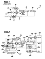
- FIG. 1 shows a prior-art digital pattern tester 10 for testing logical integrity of an input signal 14 input into the tester.
- tester 10 could be part of the design of a high-speed digital communications device (not shown), or it could be a standalone piece of equipment, such as a BERT or logic analyzer.
- the front-end of tester 10 is a voltage comparator 18 that "slices" the voltage of incoming signal 14 and recovers a logical value from it.
- the logical value is "1" when the input signal is larger than the voltage threshold of comparator 18 and "0" otherwise.
- the logical value is then compared, bit for bit, to a reference pattern 26 stored in an onboard memory 30.
- An error counter 34 keeps track of the number of mismatches between the logical values derived from input signal 14 on the one hand and the corresponding respective bits of reference pattern 26 on the other.
- Digital comparator 22 is clocked by an onboard clock signal 38 that is centered at the middle of the data bit that is being compared. This minimizes the likelihood of a sampling error.
- the centering operation either happens with delay lines (not shown) on the clock signal or with a phase tracking circuit (not shown), such as a clock-and-data recovery (CDR) circuit.
- CDR clock-and-data recovery
- a digital pattern alignment block (not shown) that shifts reference pattern 26 until the least amount of errors is observed.
- reference clock 42 provided to tester 10 can be at a low frequency, with subsequent multiplication, typically using a phase-locked loop (PLL) multiplier 46, to the target high-speed frequency.
- multiplication can increase a 100 MHz clock signal to a 5 GHz sampling signal.
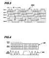
- FIG. 2 this figure shows an exemplary digital pattern testing system 200 that includes an oscilloscope feature that enables the capture of oscilloscope traces of transition or non-transition bits.
- exemplary testing system 200 is based on the design of pattern tester 10 of FIG. 1 , the major components of which are located within the dashed outline 204. That is, like tester 10 of FIG. 1 , testing system 200 of FIG. 2 includes a front end voltage comparator 208, a reference pattern memory 212, a digital comparator 216, a frequency-scaling PLL multiplier 220, and an error counter 224. As can further be seen comparing FIGS.
- input 228 of PLL multiplier 220 is preceded by a multiplexer 236 and other components as described below to provide a high-frequency time-base generator 240, which may be, for example, any one of the time-base generators described in U.S. Patent No. 7 681 091 filed on July 12,2007 , and titled "Signal Integrity Measurement Systems And Methods Using A Predominantly Digital Time-Base Generator,” for all that it discloses relative to time-base generators.
- multiplexer 236 is responsive to a selection signal 244 that continually selects between two inputs, which in this case are two versions of an incoming reference clock signal 248, an undelayed version 248A and a coarsely delayed version 248B that is delayed using a coarse delay 252.
- Coarse delay is defined as any delay that is substantially larger than the minimum delay that can be reliably constructed using conventional technology. Typically, such delay is equivalent to minimum bit period in a high speed communications device.
- the selectable input signals to multiplexer 236 may be any two or more clock signals that are coarsely delayed relative to one another.
- selection signal 244 comes from an onboard circulating memory 256 that is clocked by incoming reference clock 248.
- the combination of PLL multiplier 220, multiplexer 236, coarse delay 252 to create the delayed version 248B of clock signal 248, selection signal 244, and onboard memory 256 driving the selection signal constitute a time-base generator 240 that replaces any analog delay lines that are required in a conventional system.
- the digital logic down stream of voltage comparator 208 is modified, for example, as shown in FIG. 2 .
- the reference pattern 260 can be replaced by a constant logical value, such as 0.
- Selection between the oscilloscope mode and the bit-pattern testing mode can be facilitated, for example, by a multiplexer 264 that allows selection between the constant logical 0 signal and the output of reference pattern memory 212.
- Digital comparator 216 can remain the same as digital comparator 22 of FIG. 1 for simplicity if desired.
- error counter 224 may be bypassed and replaced by a sub-sampling flip-flop 268.
- sub-sampling flip-flop 268 serves the function of locking onto a single bit in the high-speed pattern being tested.
- sub-sampling flip-flop 268 is driven by a bit-shift and frequency-divider block 272 responsive to the output 276 of time-base generator 240.
- the frequency division of bit-shift and frequency-divider block 272 is set to a value equal to the length B of pattern 260. If pattern 260 is a pseudo-random bit sequence (PRBS) having a pattern length B of 127 bits, the frequency divider value is 127.
- PRBS pseudo-random bit sequence
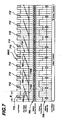
- FIG. 3 shows the operation of bit-shift and frequency-divider block 272 ( FIG. 2 ) for a pattern 260A having length B of 11.
- sub-sampling flip flop 268 FIG. 2 ) only looks at the digital comparison result every 11 data beats, instead of every data beat. It only looks at the comparison result for a single bit in the whole repeating pattern 260A.
- the output of the sub-sampled comparison operation may be accumulated in an accumulation memory 280 having an address counter 284 clocked by time-base generator 240.
- address counter 284 clocked by time-base generator 240.
- the importance of addressing using address counter 284 this way is described below. For now, its is noted that because division ratio of bit-shift and frequency-divider block 272 is equal to pattern length B in FIG. 2 , the accumulation results may arrive into accumulation memory 280 out of order, but if certain guidelines are followed, all locations in the memory will be covered (see below).
- each time PLL multiplier 220 toggles its output 276 is slightly delayed.
- every time voltage comparator 208 is clocked, it strobes the incoming bit stream of input signal 288 at a slightly different delay.
- every time sub-sampling flip flop 268 is clocked with the slowed-down clock of bit-shift and frequency-divider block 272, it, too, corresponds to a slightly different delay.
- time-base generator 240 is programmed to generate a constant ramp (see the '825 patent application for a description of programming a time-base generator), the output 276 of PLL multiplier 220 is constantly advanced or delayed by a fixed amount according to the ramp behavior.
- accumulation memory 280 Each entry in accumulation memory 280 is designed to correspond to a single delay value out of PLL multiplier 220. Thus, and referring to FIG. 4 , at the termination of one complete sweep of the time-base ramp, accumulation memory 280 will contain a time-domain waveform 400 corresponding to whether or not the transition bit being zoomed onto is higher than the voltage threshold of voltage comparator 208 ( FIG. 2 ).
- FIG. 5 illustrates the setting of the threshold voltage of voltage comparator 208 ( FIG. 2 ) to a fixed value VB and running time-base generator 240 for a bit 500 of interest of data pattern 260B.
- the result is a sequence 504 of ones and zeros that may be stored in accumulation memory 280. Incrementing the threshold voltage of voltage comparator 208 and re-running time-base generator 240, another sequence of ones and zeros is generated, and it is added to the previous set.
- thermometer code like the thermometer code 600 shown in FIG. 6 is obtained.
- the values of the thermometer code are directly accumulated in accumulation memory 280. It should be noted that this operation is different from the operation of generating bit error rate (BER) contour plots. This operation is literally a digitization operation of a repetitive voltage transition. It does not represent an error count the way a BER does.
- BER bit error rate
- FIG. 7 shows an exemplary test pattern 260C ( FIG.
- exemplary time delay values 700 outputted by the time-base generator 240 exemplary time delay values 700 outputted by the time-base generator 240, exemplary memory address values 704, and the order 708 in which the memory values are filled.
- pattern 260C has a length B of 5 bits and a bit 712 of interest.
- Time-base generator 240 ramps through its various delays in a duration equivalent to 8 bit-values.
- all memory values 704 are eventually filled as long as the sufficient number of iterations of the PLL ramp and of the bit stream is sequenced. If the length of accumulation memory 280 is not selected properly, aliasing effects occur, and erroneous measurements are made.
- the number of iterations of the time-base ramp or the bit pattern 260C corresponds to the least common multiple between the pattern length B and the time-base span N.
- the least common multiple between 5 and 8 is 40. So, 8 iterations of pattern 260C (or 5 of the time-base ramp) are required.
- FIG. 7 notice how, at the start 716A of the timing waveform 716 shown, as PLL multiplier 220 keeps toggling and ramping its output delay, it comes across the bit of interest 712 (transition of interest) twice. This means that voltage comparator 208 samples that particular bit 712 (transition) with a small delay at first, then with a large delay subsequently. In the next iteration 716B of the ramp timing waveform 716, PLL multiplier 220 comes across the same transition repetitively again, but each time it does so, it does it with a unique one of delay value 700.
- Length B of bit pattern 260 can be much smaller (e.g. 5 in the example above) or much larger (e.g., thousands of bits).
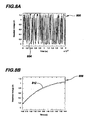
- FIG. 8A shows an example of an output plot 800 of example digital bit stream 804 as generated using the oscilloscope functionality of an oscilloscope-enabled testing system made in accordance with the present disclosure, such as digital pattern testing system 200 of FIG. 2 .
- bit stream 804 shows slow rise time and significant voltage noise. These effects are examples of what is being tested using an oscilloscope-enabled testing system of the present disclosure.
- FIG. 8B shows an example of plot 808 generated by an oscilloscope-enhanced testing system of the present disclosure, such as digital pattern testing system 200 of FIG. 2 , when the testing system is zoomed in onto a rising transition 812.
- FIG. 8A shows an example of an output plot 800 of example digital bit stream 804 as generated using the oscilloscope functionality of an oscilloscope-enabled testing system made in accordance with the present disclosure, such as digital pattern testing system 200 of FIG. 2 .
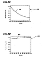
- FIG. 8C shows an example of plot 816 generated by an oscilloscope-enhanced testing system of the present disclosure, such as digital pattern testing system 200 of FIG. 2 , when the testing system is zoomed in onto a falling transition 820.
- FIGS. 8D and 8E show, respectively, exemplary plots 824, 828 generated by an oscilloscope-enhanced testing system of the present disclosure, such as digital pattern testing system 200 of FIG. 2 , when the testing system is zoomed in onto constant high and constant low bit values 832, 836, respectively.
- an oscilloscope-enabled testing system of the present disclosure has great utility in identifying problem areas in a digital bit stream.
- data-dependent jitter can easily be extracted since, now, the average arrival time of each transition in a bit stream is made available.
- FIG. 9 shows an example plot 900 containing an overlay of two rising transitions 904, 908 that exhibit data-dependent jitter.
- transitions 904, 908 occur at different times.
- histograms on particular edges can be extracted to learn about jitter parameters that are non-data-dependent.
- all transition edges can be accumulated together to generate eye masks or eye diagrams.
Landscapes
- Engineering & Computer Science (AREA)
- General Engineering & Computer Science (AREA)
- Physics & Mathematics (AREA)
- General Physics & Mathematics (AREA)
- Tests Of Electronic Circuits (AREA)
Applications Claiming Priority (3)
| Application Number | Priority Date | Filing Date | Title |
|---|---|---|---|
| US83079706P | 2006-07-14 | 2006-07-14 | |
| US11/776,865 US7813297B2 (en) | 2006-07-14 | 2007-07-12 | High-speed signal testing system having oscilloscope functionality |
| PCT/US2007/073458 WO2008008952A2 (en) | 2006-07-14 | 2007-07-13 | High-speed signal testing system having oscilloscope functionality |
Publications (3)
| Publication Number | Publication Date |
|---|---|
| EP2041584A2 EP2041584A2 (en) | 2009-04-01 |
| EP2041584A4 EP2041584A4 (en) | 2011-04-20 |
| EP2041584B1 true EP2041584B1 (en) | 2012-09-05 |
Family
ID=38924225
Family Applications (1)
| Application Number | Title | Priority Date | Filing Date |
|---|---|---|---|
| EP07799568A Not-in-force EP2041584B1 (en) | 2006-07-14 | 2007-07-13 | High-speed signal testing system having oscilloscope functionality |
Country Status (5)
| Country | Link |
|---|---|
| US (1) | US7813297B2 (zh) |
| EP (1) | EP2041584B1 (zh) |
| JP (1) | JP2009544040A (zh) |
| CA (1) | CA2657154A1 (zh) |
| WO (1) | WO2008008952A2 (zh) |
Families Citing this family (11)
| Publication number | Priority date | Publication date | Assignee | Title |
|---|---|---|---|---|
| US8327204B2 (en) | 2005-10-27 | 2012-12-04 | Dft Microsystems, Inc. | High-speed transceiver tester incorporating jitter injection |
| US7681091B2 (en) | 2006-07-14 | 2010-03-16 | Dft Microsystems, Inc. | Signal integrity measurement systems and methods using a predominantly digital time-base generator |
| US20080192814A1 (en) * | 2007-02-09 | 2008-08-14 | Dft Microsystems, Inc. | System and Method for Physical-Layer Testing of High-Speed Serial Links in their Mission Environments |
| US7917319B2 (en) * | 2008-02-06 | 2011-03-29 | Dft Microsystems Inc. | Systems and methods for testing and diagnosing delay faults and for parametric testing in digital circuits |
| US7911970B2 (en) * | 2009-02-02 | 2011-03-22 | Harvey Timothy J | Systems and methods for presenting electronic communication packets using a logic analyzer |
| US8639461B2 (en) * | 2009-09-14 | 2014-01-28 | International Business Machines Corporation | Jitter digitizer |
| US8630821B2 (en) * | 2011-07-25 | 2014-01-14 | Qualcomm Incorporated | High speed data testing without high speed bit clock |
| US8995514B1 (en) * | 2012-09-28 | 2015-03-31 | Xilinx, Inc. | Methods of and circuits for analyzing a phase of a clock signal for receiving data |
| US10411716B2 (en) | 2016-06-06 | 2019-09-10 | Richwave Technology Corp. | Subsampling motion detector for detecting motion of object under measurement |
| US9748967B1 (en) | 2017-03-02 | 2017-08-29 | Guzik Technical Enterprises | Periodic signal averaging with a time interleaving analog to digital converter |
| CN113377340B (zh) * | 2021-05-12 | 2022-10-18 | 电子科技大学 | 一种具有分数阶微积分运算和显示功能的数字示波器 |
Family Cites Families (75)
| Publication number | Priority date | Publication date | Assignee | Title |
|---|---|---|---|---|
| US3778714A (en) * | 1972-05-30 | 1973-12-11 | N Mchenry | Apparatus for detecting and counting coincidence of incoming logic signals |
| US3931610A (en) * | 1973-11-29 | 1976-01-06 | Teletype Corporation | Capacitive keyswitch sensor and method |
| US3976940A (en) | 1975-02-25 | 1976-08-24 | Fairchild Camera And Instrument Corporation | Testing circuit |
| US7663502B2 (en) * | 1992-05-05 | 2010-02-16 | Intelligent Technologies International, Inc. | Asset system control arrangement and method |
| US4807147A (en) * | 1983-10-20 | 1989-02-21 | Burr-Brown Corporation | Sampling wave-form digitizer for dynamic testing of high speed data conversion components |
| DE3481472D1 (de) * | 1984-12-21 | 1990-04-05 | Ibm | Digitale phasenregelschleife. |
| JPH0614065A (ja) * | 1992-06-26 | 1994-01-21 | Nec Corp | 多値fsk変調器 |
| JP3030598B2 (ja) * | 1994-06-24 | 2000-04-10 | アンリツ株式会社 | ジッタ検出装置 |
| US5517147A (en) * | 1994-11-17 | 1996-05-14 | Unisys Corporation | Multiple-phase clock signal generator for integrated circuits, comprising PLL, counter, and logic circuits |
| US5835501A (en) * | 1996-03-04 | 1998-11-10 | Pmc-Sierra Ltd. | Built-in test scheme for a jitter tolerance test of a clock and data recovery unit |
| US6026350A (en) * | 1996-08-30 | 2000-02-15 | Hewlett Packard Company | Self-framing serial trigger for an oscilloscope or the like |
| US6008703A (en) * | 1997-01-31 | 1999-12-28 | Massachusetts Institute Of Technology | Digital compensation for wideband modulation of a phase locked loop frequency synthesizer |
| US6076175A (en) * | 1997-03-31 | 2000-06-13 | Sun Microsystems, Inc. | Controlled phase noise generation method for enhanced testability of clock and data generator and recovery circuits |
| US5883523A (en) * | 1997-04-29 | 1999-03-16 | Credence Systems Corporation | Coherent switching power for an analog circuit tester |
| US5948115A (en) * | 1998-01-30 | 1999-09-07 | Credence Systems Corporation | Event phase modulator for integrated circuit tester |
| AU2488299A (en) * | 1998-01-30 | 1999-08-16 | Wavecrest Corporation | Method and apparatus for jitter analysis |
| US6057679A (en) * | 1998-06-12 | 2000-05-02 | Credence Systems Corporation | Integrated circuit tester having amorphous logic for real-time data analysis |
| US6181267B1 (en) * | 1998-09-30 | 2001-01-30 | Agilent Technologies Inc. | Internally triggered equivalent-time sampling system for signals having a predetermined data rate |
| EP1001533B1 (en) * | 1998-11-14 | 2001-09-26 | Agilent Technologies Inc. a Delaware Corporation | Timing generator |
| JP2000244309A (ja) * | 1999-02-18 | 2000-09-08 | Mitsubishi Electric Corp | クロック生成回路および半導体装置 |
| JP4146965B2 (ja) * | 1999-05-17 | 2008-09-10 | 株式会社アドバンテスト | 遅延信号生成装置および半導体試験装置 |
| US6091671A (en) * | 1999-07-14 | 2000-07-18 | Guide Technology, Inc. | Time interval analyzer having interpolator with constant current capacitor control |
| US6374388B1 (en) * | 1999-09-10 | 2002-04-16 | Agilent Technologies, Inc. | Equivalent time capture scheme for bit patterns within high data rate signals |
| US6865222B1 (en) * | 1999-09-23 | 2005-03-08 | Texas Instruments Incorporated | Method and apparatus for testing a serial transmitter circuit |
| US6731667B1 (en) * | 1999-11-18 | 2004-05-04 | Anapass Inc. | Zero-delay buffer circuit for a spread spectrum clock system and method therefor |
| US6640193B2 (en) * | 1999-12-15 | 2003-10-28 | Texas Instruments Incorporated | Method and system for measuring jitter |
| US6629274B1 (en) * | 1999-12-21 | 2003-09-30 | Intel Corporation | Method and apparatus to structurally detect random defects that impact AC I/O timings in an input/output buffer |
| US6834367B2 (en) * | 1999-12-22 | 2004-12-21 | International Business Machines Corporation | Built-in self test system and method for high speed clock and data recovery circuit |
| US6329850B1 (en) * | 1999-12-27 | 2001-12-11 | Texas Instruments Incorporated | Precision frequency and phase synthesis |
| US7102892B2 (en) * | 2000-03-13 | 2006-09-05 | Legacy Electronics, Inc. | Modular integrated circuit chip carrier |
| US6326993B1 (en) * | 2000-03-15 | 2001-12-04 | Toshiba Tec Kabushiki Kaisha | Pulse width modulation system and image forming apparatus having the pulse width modulation system |
| US6816987B1 (en) * | 2000-03-25 | 2004-11-09 | Broadcom Corporation | Apparatus and method for built-in self-test of a data communications system |
| JP4291494B2 (ja) * | 2000-04-04 | 2009-07-08 | 株式会社アドバンテスト | Ic試験装置のタイミング校正装置 |
| US6931579B2 (en) * | 2000-04-28 | 2005-08-16 | Mcgill University | Integrated excitation/extraction system for test and measurement |
| JP2001339282A (ja) * | 2000-05-30 | 2001-12-07 | Advantest Corp | 可変遅延回路及び半導体回路試験装置 |
| JP2002076855A (ja) * | 2000-08-29 | 2002-03-15 | Advantest Corp | 遅延回路、試験装置、コンデンサ |
| JP4310036B2 (ja) * | 2000-09-07 | 2009-08-05 | 株式会社アドバンテスト | タイミング信号発生回路、及び、それを備えた半導体検査装置 |
| GB0026614D0 (en) * | 2000-10-31 | 2000-12-13 | Lsi Logic Europ Ltd | A method and apparatus for estimation of error in data recovery schemes |
| GB2369940B (en) * | 2000-12-09 | 2004-10-20 | Mitel Corp | Multiple input phase lock loop with hitless reference switching |
| US6658363B2 (en) * | 2001-01-18 | 2003-12-02 | Hewlett-Packard Development Company, L.P. | Digital data pattern detection methods and arrangements |
| KR20030072407A (ko) * | 2001-02-14 | 2003-09-13 | 쟈인 에레쿠토로닉스 가부시키가이샤 | 반도체 집적회로 |
| DE60100114T2 (de) * | 2001-04-03 | 2003-10-02 | Agilent Technologies Inc., A Delaware Corp. | Filter zur Einspeisung von datenabhängigem Jitter und Pegelgeräusch |
| KR100374648B1 (ko) * | 2001-06-28 | 2003-03-03 | 삼성전자주식회사 | 전자파를 감소시키기 위한 위상동기루프회로 및 그의제어방법 |
| US6816988B2 (en) * | 2001-08-31 | 2004-11-09 | Agilent Technologies, Inc. | Method and system for minimal-time bit-error-rate testing |
| US7116851B2 (en) * | 2001-10-09 | 2006-10-03 | Infinera Corporation | Optical signal receiver, an associated photonic integrated circuit (RxPIC), and method improving performance |
| AU2002334906A1 (en) * | 2001-10-09 | 2003-04-22 | Infinera Corporation | Transmitter photonic integrated circuits (txpic) and optical transport networks employing txpics |
| JP3869699B2 (ja) * | 2001-10-24 | 2007-01-17 | 株式会社アドバンテスト | タイミング発生器、半導体試験装置、及びタイミング発生方法 |
| US6785622B2 (en) * | 2001-10-29 | 2004-08-31 | Agilent Technologies, Inc. | Method and apparatus for performing eye diagram measurements |
| US6865496B2 (en) * | 2001-11-01 | 2005-03-08 | Agilent Technologies, Inc. | Zero-crossing direction and time interval jitter measurement apparatus using offset sampling |
| JP4320139B2 (ja) * | 2001-11-13 | 2009-08-26 | 株式会社アドバンテスト | タイミング発生装置、及び試験装置 |
| DE10157437B4 (de) * | 2001-11-23 | 2007-04-26 | Infineon Technologies Ag | Schaltungsanordnung zur Takt- und Datenrückgewinnung aus einem Empfangssignal |
| US6868047B2 (en) * | 2001-12-12 | 2005-03-15 | Teradyne, Inc. | Compact ATE with time stamp system |
| US6975940B1 (en) * | 2001-12-21 | 2005-12-13 | Garmin Ltd. | Systems, functional data, and methods for generating a route |
| US6934896B2 (en) * | 2001-12-31 | 2005-08-23 | Advantest Corp. | Time shift circuit for functional and AC parametric test |
| US7426220B2 (en) * | 2002-01-09 | 2008-09-16 | L-3 Communications Corporation | Method and apparatus for aligning the clock signals of transceivers in a multiple access communication system utilizing programmable, multi-tap phase-locked loops |
| US6775809B1 (en) * | 2002-03-14 | 2004-08-10 | Rambus Inc. | Technique for determining performance characteristics of electronic systems |
| US6650101B2 (en) * | 2002-04-08 | 2003-11-18 | Agilent Technologies, Inc. | Timebase for sampling an input signal having a synchronous trigger |
| US6918073B2 (en) * | 2002-04-12 | 2005-07-12 | Agilent Technologies, Inc. | Differential self-test of input/output circuits |
| US20030198311A1 (en) * | 2002-04-19 | 2003-10-23 | Wireless Interface Technologies, Inc. | Fractional-N frequency synthesizer and method |
| JP3559785B2 (ja) * | 2002-06-17 | 2004-09-02 | Necエレクトロニクス株式会社 | Pll回路及び位相差検出回路 |
| US7136772B2 (en) * | 2002-11-08 | 2006-11-14 | Avago Technologies Fiber Ip (Singapore) Pte. Ltd. | Monitoring system for a communications network |
| US6909316B2 (en) * | 2003-02-21 | 2005-06-21 | Agilent Technologies, Inc. | Variable delay circuit with high resolution |
| US6909980B2 (en) * | 2003-03-13 | 2005-06-21 | Agilent Technologies, Inc. | Auto skew alignment of high-speed differential eye diagrams |
| US6768390B1 (en) * | 2003-04-02 | 2004-07-27 | Agilent Technologies, Inc. | System and method for generating balanced modulated signals with arbitrary amplitude and phase control using modulation |
| US7092472B2 (en) * | 2003-09-16 | 2006-08-15 | Rambus Inc. | Data-level clock recovery |
| JP3982461B2 (ja) | 2003-06-12 | 2007-09-26 | 横河電機株式会社 | アナログディジタル変換器 |
| US7403486B2 (en) * | 2003-10-31 | 2008-07-22 | Acterna | Signal level measurement and data connection quality analysis apparatus and methods |
| JP3902185B2 (ja) * | 2004-03-01 | 2007-04-04 | 日本電気株式会社 | 電源ノイズ測定装置 |
| US20060139387A1 (en) * | 2004-05-27 | 2006-06-29 | Silverbrook Research Pty Ltd | Printer controller for providing data and command via communication output |
| GB0413146D0 (en) * | 2004-06-12 | 2004-07-14 | Texas Instruments Ltd | Comparator for circuit testing |
| JP4425735B2 (ja) * | 2004-07-22 | 2010-03-03 | 株式会社アドバンテスト | ジッタ印加回路、及び試験装置 |
| DE602004008080T2 (de) * | 2004-10-27 | 2008-04-17 | Agilent Technologies, Inc. (n.d.Ges.d. Staates Delaware), Santa Clara | Mit einer Quelle synchrone Abtastung |
| US8327204B2 (en) * | 2005-10-27 | 2012-12-04 | Dft Microsystems, Inc. | High-speed transceiver tester incorporating jitter injection |
| US7681091B2 (en) * | 2006-07-14 | 2010-03-16 | Dft Microsystems, Inc. | Signal integrity measurement systems and methods using a predominantly digital time-base generator |
| US20080192814A1 (en) * | 2007-02-09 | 2008-08-14 | Dft Microsystems, Inc. | System and Method for Physical-Layer Testing of High-Speed Serial Links in their Mission Environments |
-
2007
- 2007-07-12 US US11/776,865 patent/US7813297B2/en not_active Expired - Fee Related
- 2007-07-13 JP JP2009520920A patent/JP2009544040A/ja active Pending
- 2007-07-13 CA CA002657154A patent/CA2657154A1/en not_active Abandoned
- 2007-07-13 WO PCT/US2007/073458 patent/WO2008008952A2/en active Application Filing
- 2007-07-13 EP EP07799568A patent/EP2041584B1/en not_active Not-in-force
Also Published As
| Publication number | Publication date |
|---|---|
| EP2041584A4 (en) | 2011-04-20 |
| CA2657154A1 (en) | 2008-01-17 |
| WO2008008952A3 (en) | 2008-08-28 |
| WO2008008952A2 (en) | 2008-01-17 |
| US7813297B2 (en) | 2010-10-12 |
| JP2009544040A (ja) | 2009-12-10 |
| EP2041584A2 (en) | 2009-04-01 |
| US20080013456A1 (en) | 2008-01-17 |
Similar Documents
| Publication | Publication Date | Title |
|---|---|---|
| EP2041584B1 (en) | High-speed signal testing system having oscilloscope functionality | |
| TWI440858B (zh) | 測試高速重複的資料訊號之系統及使用示波器分析高速資料訊號之方法 | |
| US7681091B2 (en) | Signal integrity measurement systems and methods using a predominantly digital time-base generator | |
| US7158899B2 (en) | Circuit and method for measuring jitter of high speed signals | |
| US7496137B2 (en) | Apparatus for measuring jitter and method of measuring jitter | |
| US8489947B2 (en) | Circuit and method for simultaneously measuring multiple changes in delay | |
| US7574632B2 (en) | Strobe technique for time stamping a digital signal | |
| WO2006023756A1 (en) | Time measurement using phase shifted periodic waveforms | |
| US9838165B2 (en) | Emulation and debug interfaces for testing an integrated circuit with an asynchronous microcontroller | |
| US7856578B2 (en) | Strobe technique for test of digital signal timing | |
| CN111123083B (zh) | 一种针对fpga pll ip核的测试系统及方法 | |
| EP1927204A2 (en) | Strobe technique for time stamping a digital signal | |
| US7945404B2 (en) | Clock jitter measurement circuit and integrated circuit having the same | |
| US7143323B2 (en) | High speed capture and averaging of serial data by asynchronous periodic sampling | |
| US7661052B2 (en) | Using statistical signatures for testing high-speed circuits | |
| EP1847844A1 (en) | Digital data signal analysis by evaluating sampled values in conjuction with signal bit values | |
| EP1847843B1 (en) | Digital data sampling by applying a plurality of time delayed trigger signals | |
| EP1812803B1 (en) | Testable integrated circuit | |
| EP1845385B1 (en) | Time interval analysis of digital data |
Legal Events
| Date | Code | Title | Description |
|---|---|---|---|
| PUAI | Public reference made under article 153(3) epc to a published international application that has entered the european phase |
Free format text: ORIGINAL CODE: 0009012 |
|
| 17P | Request for examination filed |
Effective date: 20090127 |
|
| AK | Designated contracting states |
Kind code of ref document: A2 Designated state(s): AT BE BG CH CY CZ DE DK EE ES FI FR GB GR HU IE IS IT LI LT LU LV MC MT NL PL PT RO SE SI SK TR |
|
| AX | Request for extension of the european patent |
Extension state: AL BA HR MK RS |
|
| DAX | Request for extension of the european patent (deleted) | ||
| A4 | Supplementary search report drawn up and despatched |
Effective date: 20110322 |
|
| RIC1 | Information provided on ipc code assigned before grant |
Ipc: G01R 31/3193 20060101AFI20110316BHEP |
|
| REG | Reference to a national code |
Ref country code: DE Ref legal event code: R079 Ref document number: 602007025317 Country of ref document: DE Free format text: PREVIOUS MAIN CLASS: G01R0019000000 Ipc: G01R0031319300 |
|
| GRAP | Despatch of communication of intention to grant a patent |
Free format text: ORIGINAL CODE: EPIDOSNIGR1 |
|
| RIC1 | Information provided on ipc code assigned before grant |
Ipc: H04L 12/26 20060101ALI20120123BHEP Ipc: G01R 31/3177 20060101ALI20120123BHEP Ipc: G01R 31/3193 20060101AFI20120123BHEP |
|
| GRAS | Grant fee paid |
Free format text: ORIGINAL CODE: EPIDOSNIGR3 |
|
| GRAA | (expected) grant |
Free format text: ORIGINAL CODE: 0009210 |
|
| AK | Designated contracting states |
Kind code of ref document: B1 Designated state(s): AT BE BG CH CY CZ DE DK EE ES FI FR GB GR HU IE IS IT LI LT LU LV MC MT NL PL PT RO SE SI SK TR |
|
| REG | Reference to a national code |
Ref country code: GB Ref legal event code: FG4D |
|
| REG | Reference to a national code |
Ref country code: CH Ref legal event code: EP |
|
| REG | Reference to a national code |
Ref country code: AT Ref legal event code: REF Ref document number: 574345 Country of ref document: AT Kind code of ref document: T Effective date: 20120915 |
|
| REG | Reference to a national code |
Ref country code: IE Ref legal event code: FG4D |
|
| REG | Reference to a national code |
Ref country code: DE Ref legal event code: R096 Ref document number: 602007025317 Country of ref document: DE Effective date: 20121031 |
|
| REG | Reference to a national code |
Ref country code: AT Ref legal event code: MK05 Ref document number: 574345 Country of ref document: AT Kind code of ref document: T Effective date: 20120905 |
|
| REG | Reference to a national code |
Ref country code: NL Ref legal event code: VDEP Effective date: 20120905 |
|
| PG25 | Lapsed in a contracting state [announced via postgrant information from national office to epo] |
Ref country code: LT Free format text: LAPSE BECAUSE OF FAILURE TO SUBMIT A TRANSLATION OF THE DESCRIPTION OR TO PAY THE FEE WITHIN THE PRESCRIBED TIME-LIMIT Effective date: 20120905 Ref country code: CY Free format text: LAPSE BECAUSE OF FAILURE TO SUBMIT A TRANSLATION OF THE DESCRIPTION OR TO PAY THE FEE WITHIN THE PRESCRIBED TIME-LIMIT Effective date: 20120905 Ref country code: AT Free format text: LAPSE BECAUSE OF FAILURE TO SUBMIT A TRANSLATION OF THE DESCRIPTION OR TO PAY THE FEE WITHIN THE PRESCRIBED TIME-LIMIT Effective date: 20120905 Ref country code: FI Free format text: LAPSE BECAUSE OF FAILURE TO SUBMIT A TRANSLATION OF THE DESCRIPTION OR TO PAY THE FEE WITHIN THE PRESCRIBED TIME-LIMIT Effective date: 20120905 |
|
| REG | Reference to a national code |
Ref country code: LT Ref legal event code: MG4D Effective date: 20120905 |
|
| PG25 | Lapsed in a contracting state [announced via postgrant information from national office to epo] |
Ref country code: SE Free format text: LAPSE BECAUSE OF FAILURE TO SUBMIT A TRANSLATION OF THE DESCRIPTION OR TO PAY THE FEE WITHIN THE PRESCRIBED TIME-LIMIT Effective date: 20120905 Ref country code: SI Free format text: LAPSE BECAUSE OF FAILURE TO SUBMIT A TRANSLATION OF THE DESCRIPTION OR TO PAY THE FEE WITHIN THE PRESCRIBED TIME-LIMIT Effective date: 20120905 Ref country code: GR Free format text: LAPSE BECAUSE OF FAILURE TO SUBMIT A TRANSLATION OF THE DESCRIPTION OR TO PAY THE FEE WITHIN THE PRESCRIBED TIME-LIMIT Effective date: 20121206 Ref country code: LV Free format text: LAPSE BECAUSE OF FAILURE TO SUBMIT A TRANSLATION OF THE DESCRIPTION OR TO PAY THE FEE WITHIN THE PRESCRIBED TIME-LIMIT Effective date: 20120905 |
|
| PG25 | Lapsed in a contracting state [announced via postgrant information from national office to epo] |
Ref country code: IS Free format text: LAPSE BECAUSE OF FAILURE TO SUBMIT A TRANSLATION OF THE DESCRIPTION OR TO PAY THE FEE WITHIN THE PRESCRIBED TIME-LIMIT Effective date: 20130105 Ref country code: CZ Free format text: LAPSE BECAUSE OF FAILURE TO SUBMIT A TRANSLATION OF THE DESCRIPTION OR TO PAY THE FEE WITHIN THE PRESCRIBED TIME-LIMIT Effective date: 20120905 Ref country code: RO Free format text: LAPSE BECAUSE OF FAILURE TO SUBMIT A TRANSLATION OF THE DESCRIPTION OR TO PAY THE FEE WITHIN THE PRESCRIBED TIME-LIMIT Effective date: 20120905 Ref country code: EE Free format text: LAPSE BECAUSE OF FAILURE TO SUBMIT A TRANSLATION OF THE DESCRIPTION OR TO PAY THE FEE WITHIN THE PRESCRIBED TIME-LIMIT Effective date: 20120905 Ref country code: NL Free format text: LAPSE BECAUSE OF FAILURE TO SUBMIT A TRANSLATION OF THE DESCRIPTION OR TO PAY THE FEE WITHIN THE PRESCRIBED TIME-LIMIT Effective date: 20120905 Ref country code: BE Free format text: LAPSE BECAUSE OF FAILURE TO SUBMIT A TRANSLATION OF THE DESCRIPTION OR TO PAY THE FEE WITHIN THE PRESCRIBED TIME-LIMIT Effective date: 20120905 |
|
| PG25 | Lapsed in a contracting state [announced via postgrant information from national office to epo] |
Ref country code: SK Free format text: LAPSE BECAUSE OF FAILURE TO SUBMIT A TRANSLATION OF THE DESCRIPTION OR TO PAY THE FEE WITHIN THE PRESCRIBED TIME-LIMIT Effective date: 20120905 Ref country code: PL Free format text: LAPSE BECAUSE OF FAILURE TO SUBMIT A TRANSLATION OF THE DESCRIPTION OR TO PAY THE FEE WITHIN THE PRESCRIBED TIME-LIMIT Effective date: 20120905 Ref country code: PT Free format text: LAPSE BECAUSE OF FAILURE TO SUBMIT A TRANSLATION OF THE DESCRIPTION OR TO PAY THE FEE WITHIN THE PRESCRIBED TIME-LIMIT Effective date: 20130107 |
|
| PLBE | No opposition filed within time limit |
Free format text: ORIGINAL CODE: 0009261 |
|
| STAA | Information on the status of an ep patent application or granted ep patent |
Free format text: STATUS: NO OPPOSITION FILED WITHIN TIME LIMIT |
|
| PG25 | Lapsed in a contracting state [announced via postgrant information from national office to epo] |
Ref country code: BG Free format text: LAPSE BECAUSE OF FAILURE TO SUBMIT A TRANSLATION OF THE DESCRIPTION OR TO PAY THE FEE WITHIN THE PRESCRIBED TIME-LIMIT Effective date: 20121205 Ref country code: DK Free format text: LAPSE BECAUSE OF FAILURE TO SUBMIT A TRANSLATION OF THE DESCRIPTION OR TO PAY THE FEE WITHIN THE PRESCRIBED TIME-LIMIT Effective date: 20120905 |
|
| 26N | No opposition filed |
Effective date: 20130606 |
|
| PG25 | Lapsed in a contracting state [announced via postgrant information from national office to epo] |
Ref country code: IT Free format text: LAPSE BECAUSE OF FAILURE TO SUBMIT A TRANSLATION OF THE DESCRIPTION OR TO PAY THE FEE WITHIN THE PRESCRIBED TIME-LIMIT Effective date: 20120905 |
|
| REG | Reference to a national code |
Ref country code: DE Ref legal event code: R097 Ref document number: 602007025317 Country of ref document: DE Effective date: 20130606 |
|
| PG25 | Lapsed in a contracting state [announced via postgrant information from national office to epo] |
Ref country code: ES Free format text: LAPSE BECAUSE OF FAILURE TO SUBMIT A TRANSLATION OF THE DESCRIPTION OR TO PAY THE FEE WITHIN THE PRESCRIBED TIME-LIMIT Effective date: 20121216 |
|
| PG25 | Lapsed in a contracting state [announced via postgrant information from national office to epo] |
Ref country code: MC Free format text: LAPSE BECAUSE OF FAILURE TO SUBMIT A TRANSLATION OF THE DESCRIPTION OR TO PAY THE FEE WITHIN THE PRESCRIBED TIME-LIMIT Effective date: 20120905 |
|
| REG | Reference to a national code |
Ref country code: CH Ref legal event code: PL |
|
| GBPC | Gb: european patent ceased through non-payment of renewal fee |
Effective date: 20130713 |
|
| REG | Reference to a national code |
Ref country code: IE Ref legal event code: MM4A |
|
| REG | Reference to a national code |
Ref country code: DE Ref legal event code: R119 Ref document number: 602007025317 Country of ref document: DE Effective date: 20140201 |
|
| REG | Reference to a national code |
Ref country code: FR Ref legal event code: ST Effective date: 20140331 |
|
| PG25 | Lapsed in a contracting state [announced via postgrant information from national office to epo] |
Ref country code: CH Free format text: LAPSE BECAUSE OF NON-PAYMENT OF DUE FEES Effective date: 20130731 Ref country code: LI Free format text: LAPSE BECAUSE OF NON-PAYMENT OF DUE FEES Effective date: 20130731 Ref country code: DE Free format text: LAPSE BECAUSE OF NON-PAYMENT OF DUE FEES Effective date: 20140201 Ref country code: GB Free format text: LAPSE BECAUSE OF NON-PAYMENT OF DUE FEES Effective date: 20130713 |
|
| PG25 | Lapsed in a contracting state [announced via postgrant information from national office to epo] |
Ref country code: FR Free format text: LAPSE BECAUSE OF NON-PAYMENT OF DUE FEES Effective date: 20130731 |
|
| PG25 | Lapsed in a contracting state [announced via postgrant information from national office to epo] |
Ref country code: IE Free format text: LAPSE BECAUSE OF NON-PAYMENT OF DUE FEES Effective date: 20130713 |
|
| PG25 | Lapsed in a contracting state [announced via postgrant information from national office to epo] |
Ref country code: TR Free format text: LAPSE BECAUSE OF FAILURE TO SUBMIT A TRANSLATION OF THE DESCRIPTION OR TO PAY THE FEE WITHIN THE PRESCRIBED TIME-LIMIT Effective date: 20120905 Ref country code: MT Free format text: LAPSE BECAUSE OF FAILURE TO SUBMIT A TRANSLATION OF THE DESCRIPTION OR TO PAY THE FEE WITHIN THE PRESCRIBED TIME-LIMIT Effective date: 20120905 |
|
| PG25 | Lapsed in a contracting state [announced via postgrant information from national office to epo] |
Ref country code: HU Free format text: LAPSE BECAUSE OF FAILURE TO SUBMIT A TRANSLATION OF THE DESCRIPTION OR TO PAY THE FEE WITHIN THE PRESCRIBED TIME-LIMIT; INVALID AB INITIO Effective date: 20070713 Ref country code: LU Free format text: LAPSE BECAUSE OF NON-PAYMENT OF DUE FEES Effective date: 20130713 |