US5948115A - Event phase modulator for integrated circuit tester - Google Patents
Event phase modulator for integrated circuit tester Download PDFInfo
- Publication number
- US5948115A US5948115A US09/016,532 US1653298A US5948115A US 5948115 A US5948115 A US 5948115A US 1653298 A US1653298 A US 1653298A US 5948115 A US5948115 A US 5948115A
- Authority
- US
- United States
- Prior art keywords
- signal
- state
- timing signal
- pulse
- input
- Prior art date
- Legal status (The legal status is an assumption and is not a legal conclusion. Google has not performed a legal analysis and makes no representation as to the accuracy of the status listed.)
- Expired - Lifetime
Links
- 238000012360 testing method Methods 0.000 claims abstract description 116
- 230000004044 response Effects 0.000 claims abstract description 36
- 230000003111 delayed effect Effects 0.000 claims description 19
- 238000005070 sampling Methods 0.000 claims description 7
- 238000000034 method Methods 0.000 claims description 2
- 238000004519 manufacturing process Methods 0.000 claims 1
- 230000008859 change Effects 0.000 abstract description 9
- 238000010586 diagram Methods 0.000 description 17
- 230000007704 transition Effects 0.000 description 6
- 230000000694 effects Effects 0.000 description 5
- 230000006399 behavior Effects 0.000 description 2
- 230000005540 biological transmission Effects 0.000 description 2
- 238000004891 communication Methods 0.000 description 2
- 230000001934 delay Effects 0.000 description 2
- 238000012986 modification Methods 0.000 description 2
- 230000004048 modification Effects 0.000 description 2
- 230000000737 periodic effect Effects 0.000 description 2
- 238000006073 displacement reaction Methods 0.000 description 1
- 230000006870 function Effects 0.000 description 1
- 230000008520 organization Effects 0.000 description 1
- 238000011084 recovery Methods 0.000 description 1
Images


Classifications
-
- G—PHYSICS
- G11—INFORMATION STORAGE
- G11C—STATIC STORES
- G11C29/00—Checking stores for correct operation ; Subsequent repair; Testing stores during standby or offline operation
-
- G—PHYSICS
- G01—MEASURING; TESTING
- G01R—MEASURING ELECTRIC VARIABLES; MEASURING MAGNETIC VARIABLES
- G01R31/00—Arrangements for testing electric properties; Arrangements for locating electric faults; Arrangements for electrical testing characterised by what is being tested not provided for elsewhere
- G01R31/28—Testing of electronic circuits, e.g. by signal tracer
- G01R31/317—Testing of digital circuits
- G01R31/3181—Functional testing
- G01R31/319—Tester hardware, i.e. output processing circuits
- G01R31/31917—Stimuli generation or application of test patterns to the device under test [DUT]
- G01R31/31919—Storing and outputting test patterns
-
- G—PHYSICS
- G01—MEASURING; TESTING
- G01R—MEASURING ELECTRIC VARIABLES; MEASURING MAGNETIC VARIABLES
- G01R31/00—Arrangements for testing electric properties; Arrangements for locating electric faults; Arrangements for electrical testing characterised by what is being tested not provided for elsewhere
- G01R31/28—Testing of electronic circuits, e.g. by signal tracer
- G01R31/317—Testing of digital circuits
- G01R31/3181—Functional testing
- G01R31/319—Tester hardware, i.e. output processing circuits
- G01R31/31917—Stimuli generation or application of test patterns to the device under test [DUT]
- G01R31/31922—Timing generation or clock distribution
Definitions
- the present invention relates in general to integrated circuit testers and in particular to a driver circuit for producing a phase modulated test signal.
- Recoverable clock receivers are often used in high speed telecommunications systems.
- a recoverable clock transmission system uses the data transitions within a transmitted data stream to convey timing information rather than sending an additional reference clock signal in parallel with the data signal.
- the recoverable clock receiver monitors the incoming data stream to "recover" a representative copy of the clock that the transmitter used when transmitting the data stream. Pulses of the recovered clock signal tell the receiver when to sample the data stream.
- jitter is defined as a periodic time displacement error in state transitions that varies with time in a sinusoidal fashion. Thus in a "jittery” data signal the state transitions do not occur at regular intervals. When the jitter is severe enough, the receiver will not be able to recover the clock signal.
- An IC tester can test a recoverable clock receiver by sending it a data signal and sampling the receiver's output to determine if it accurately reflects the data pattern conveyed in the test signal.
- the receiver's tolerance to jitter can be measured by introducing an appropriate sinusoidal variation in the timing of state changes in the data signal.
- the speed of recoverable clock communication devices increases it has become more difficult to test receivers for jitter tolerance.
- FIG. 1 illustrates a typical "per-pin" integrated circuit tester 10 in block diagram form.
- Tester 10 includes a separate channel 11 for each pin or terminal of an integrated circuit device under test (DUT) 12.
- DUT integrated circuit device under test
- a test is organized into a sequence of test cycles, and during each test cycle each channel 11 can either generate and transmit a test signal to a DUT terminal and/or sample a DUT output signal produced at the DUT terminal to determine its state.
- a host computer 14 transmits a vector data sequence via a bus 16 to each channel 11. Each vector data sequence defines the test activities the channel is to carry out during the test. After storing a vector sequence in each channel, host computer 14 concurrently signals channels 11 to start the test. Each channel 11 then carries out the sequence of test activities defined by its stored vector data sequence.
- channels 11 synchronize their activities to a common master clock signal MCLK produced by a clock source 17.
- FIG. 2 illustrates a typical tester channel 11 of FIG. 1 in more detailed block diagram form.
- channel 11 includes a vector memory 18 for storing the vector data sequence arriving on bus 16.
- a START signal sent from host 14 of FIG. 1 via a control line of bus 16 tells a sequencer 20 to begin read addressing vector memory 18.
- Sequencer 20, clocked by the MCLK signal, sends a new address to vector memory 18 before the start of each test cycle.
- vector memory 18 reads out vector data indicating the test activity channel 11 is to carry out during a test cycle.
- the vector data also indicates a time during the test cycle at which the activity is to be carried out.
- the test vector provides input to a drive circuit 22 and a compare circuit 28.
- Drive circuit 22 produces the TEST signal output of channel 11 provided to a terminal of DUT 12 of FIG. 1.
- the VECTOR data supplied as input to drive circuit 22 at the start of each test cycle may indicate that the TEST signal is to change to a particular state at a particular time during the test cycle.
- a timing signal generator 24 using the master clock signal MCLK as a timing reference, produces a set of timing signals TS.
- Each timing signal TS has a period matching that of the test cycle, but the timing signals are evenly distributed in phase so that each timing signal pulse edge marks a different time during a test cycle.
- Timing signals TS are provided as inputs to drive circuit 22 and compare circuit 28.
- the VECTOR data indicates the timing of the TEST signal state change by telling drive circuit 22 to select a particular one of the TS signals as a trigger for the state change.
- the VECTOR data may also tell compare circuit 28 to sample the DUT output signal during the test cycle and to determine whether the sampled test signal state matches an expected state.
- the VECTOR data indicates the timing of DUT -- OUT signal sampling by telling compare circuit 28 to select one of the timing signals TS as a trigger for the sampling event.
- FIG. 3 illustrates a typical prior art drive circuit 22 of FIG. 2 in block diagram form.
- Drive circuit 22 includes a decoder 30, a pair of type D flip-flops 32 and 34, an inhibitable driver 36 and a set of multiplexers 38.
- Driver 36 produces the TEST signal in response to input DRIVE and INHIBIT signals.
- the INHIBIT signal inhibits the TEST signal when asserted.
- the DRIVE signal state controls the TEST signal state.
- Decoder 30 decodes the VECTOR arriving at the start of each test cycle to produce a pair of indicating signals; a signal D indicating a state to which the DRIVE signal is to be driven and a signal I indicating a state to which the INHIBIT signal is to be driven.
- the D and I indicating signals drive D inputs of flip-flops 32 and 34, respectively.
- Decoder 30 also signals multiplexer 38 to select a pair of timing signals TS and to provide them as signals TD and TI to clock inputs of flip-flops 32 and 34, respectively.
- Flip-flop 32 produces the DRIVE signal at its Q output and flip-flop 34 produces the INHIBIT signal at its Q output.
- decoder 30 When, for example, an arriving VECTOR indicates that the INHIBIT signal is to go low at a time T1 and the DRIVE signal is to go high at a time T2 during the next test cycle, decoder 30 immediately drives its output D signal high and its output I signal low. Decoder 30 also signals multiplexers 38 to select a timing signal TS providing a pulse at time T1 as the TI clock input to flip-flop 34 and to select another timing signal TS providing a pulse at time T2 as the TD input to flip-flop 32. Thus at time T1 the TI signal pulse clocks the I signal state onto the Q output of flip-flop 34 thereby pulling down the INHIBIT signal so as to enable driver 36. At time T2 the TD signal pulse clocks the D signal state onto the Q output of flip-flop 32 thereby setting the DRIVE signal high. Driver 36 responds by driving the TEST signal high.
- one channel's TEST signal output may be used as the signal input to the receiver.
- the compare circuit of another tester channel can be used to sample the receiver output signal.
- the vector data input to the channel producing the TEST signal is designed to produce a TEST signal conveying an appropriate data sequence to be supplied to the receiver input. We can introduce jitter into the TEST signal simply by adjusting the edge timing information conveyed in the vector data sequence so that TEST signal state changes vary with time in the desired sinusoidal fashion.
- timing resolution provided by timing signals TS produced by timing signal generator 24 of FIG. 2.
- DUT operating frequencies increase limitations in timing resolution precludes obtaining the appropriate jitter simply by designing jitter into the test event timing specified by the vector sequence defining the TEST signal behavior. What is needed is a simple and effective system for introducing a specified jitter into a TEST signal output of an integrated circuit tester.
- the present invention relates to a drive circuit that produces a phase modulated test signal for an integrated circuit tester.
- the drive circuit receives an input sequence of vector data values, each vector data value indicating a test signal state and a time at which the test signal is to change to the indicated state.
- the vector data sequence may thus define a time-varying test signal.
- the drive circuit produces a phase modulated version of the time-varying test signal defined by the vector data sequence.
- drive circuit includes a decoder, a timing signal generator, an event phase modulator and a driver for producing the test signal.
- the decoder decodes each incoming vector data value and supplies an indicating signal of state determined by the vector data value as data input to the event phase modulator.
- the decoder also signals the timing signal generator to provide a timing signal pulse input to the event phase modulator at the time indicated by the incoming vector data value.
- phase modulator samples the indicating signal to determine its state, and then after a delay, supplies an output drive signal of similar state as input to the driver.
- the drive signal controls the state of the driver's output test signal.
- the delay provided by the phase modulator is set after each incoming timing signal pulse in accordance with a pattern defined by programming data supplied as input to the phase modulator.
- the drive signal produced by the phase modulator, and therefore the test signal produced by the driver in response to the drive signal is a phase modulated version of the time-varying test signal defined by the vector data sequence, with the phase modulation being controlled by the programming data input to the phase modulator.
- the phase modulator includes a first-in, first-out (FIFO) buffer, a programmable delay circuit, and a programmable pattern generator.
- the FIFO buffer stores a control bit representing the current state of the indicating signal produced by the decoder in response to each timing signal pulse.
- the programmable delay circuit delays the timing signal with a delay determined by delay data produced by the pattern generator to provide a delayed timing signal.
- the delay data is set after each timing signal pulse in accordance with a pattern defined by programming data input to the pattern generator.
- the FIFO buffer shifts out its longest stored control bit in response to each delayed timing signal pulse.
- the control bit shifted out of the FIFO buffer controls the state of the drive signal.
- FIG. 1 illustrates a typical "per-pin" integrated circuit tester in block diagram form
- FIG. 2 illustrates a typical tester channel of FIG. 1 in more detailed block diagram form
- FIG. 3 illustrates a typical prior art drive circuit of FIG. 2 in more detailed block diagram form
- FIG. 4 illustrates, in block diagram form, a drive circuit for an integrated circuit tester in accordance with the present invention
- FIG. 5 is a timing diagram illustrating operation of the drive circuit of FIG. 4;
- FIG. 6 illustrates an event phase modulator of FIG. 4 in more detailed block diagram form
- FIG. 7 illustrates the pattern generator of FIG. 6 in more detailed block diagram form
- FIG. 8 illustrates in block diagram form an alternative embodiment of a driver circuit for an integrated circuit tester in accordance with the present invention.
- FIG. 9 illustrates an event phase modulator of FIG. 8 in more detailed block diagram form.
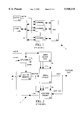
- FIG. 4 illustrates a drive circuit 40 in accordance with the present invention for a channel of an integrated circuit tester.
- Drive circuit 40 which may be used in place of drive circuit 22 of the prior art tester channel 11 of FIG. 2, produces an output TEST signal that is a phase modulated version of a test signal defined by a vector data sequence input (VECTOR) to drive circuit 40.
- the TEST signal produced by an inhibitable driver 42, may take on any of three states: logically high, logically low and inhibited.
- driver 42 drives the TEST high when an input DRIVE signal is high and drives the TEST signal low when the DRIVE signal is low.
- driver 42 does not actively produce the TEST signal.
- a test is organized into a succession of test cycles and new VECTOR data value is supplied as input to drive circuit 42 at the beginning of each test cycle.
- Each VECTOR data value may specify up to two TEST signal state changes that are to occur during the following test cycle.
- the VECTOR data value also indicates a time during the test cycle at which each TEST signal state change is to occur.
- a decoder 44 decodes each incoming VECTOR data value to produce a signal D indicating a state to which the DRIVE signal is to be driven and a signal I indicating a state to which the inhibit signal is to be driven.
- the D and I indicating signals are provided as inputs to a pair of "event phase modulators" 46 and 48, respectively.
- Event phase modulator 46 produces the DRIVE signal input to driver 42 while event phase modulator 48 produces the INHIBIT signal input to driver 42.
- a set of timing signals TS (produced for, example by timing signal generator 24 of FIG. 2) are provided as inputs to a pair of multiplexers 50. Each timing signal TS provides a single pulse at a unique time during each test cycle. Decoder 44 signals multiplexers 50 to select a pair of timing signals TS and to provide them as timing signals inputs TD and TI to event phase modulators 46 and 48, respectively.
- decoder 30 If the incoming vector indicates that the TEST signal is to be driven high or low at a particular time T1 during the next test cycle, decoder 30 signals one of multiplexers 50 to select a timing signal TS having a pulse at that particular time T1 as the TD input to event phase modulator 46. Similarly, if the incoming vector indicates that the TEST signal is to switch between active and inhibited at some particular time T2 during the next test cycle, decoder 30 signals the other one of multiplexers 50 to select a timing signal TS having a pulse at that particular time T2 as the TI input to event phase modulator 48.
- event phase modulator 46 In response to each pulse of the TD signal, event phase modulator 46 stores a control bit representing the current state of its input indicating signal D. After a delay, event phase modulator 46 sets the state of its output DRIVE signal to match the state of the control bit.
- the delay between the TD signal is pulse and any subsequent change in state of the DRIVE signal is controlled by input programming data provided to event phase modulator 46 via a computer bus 16.
- the programming data may specify the delay to be either fixed or a function of time, with its value set after each TD signal pulse.
- Event phase modulator 48 having a similar response to each pulse the TI signal, also sets the state of the INHIBIT signal to match the state of its input indicating signal I with a delay also controlled by externally generated programming data delivered via bus 16.
- driver circuit 40 can produce a TEST signal that is a phase modulated version of the TEST signal defined by the input VECTOR data sequence, with the nature of the phase modulation being determined by the programming data inputs to event phase modulators 46
- driver circuit 40 is useful, for example, in testing the jitter tolerance of a recoverable clock communications receiver.
- An IC tester employing drive circuit 40 of FIG. 4 in its channels can test a recoverable clock receiver by using one of the tester channels to send a TEST signal as the input signal to the receiver while using a comparator in a second tester channel to monitor the receiver output to determine if it is correctly detecting a data sequence conveyed by the TEST signal.
- the VECTOR data supplied to the driver 40 within the tester channel providing the receiver's input signal defines a jitter-free TEST signal in which state transitions occur at the proper times.
- FIG. 5 is a timing diagram illustrating operation of drive circuit 40 of FIG. 4 when event phase modulator 46 is programmed to provide sinusoidal phase modulation.
- the VECTOR data input to decoder 44 of FIG. 4 defines an indicating signal D of which changes state at the same relative time during each successive test cycle.
- the timing signal TD provides a pulse at the same time during each test cycle. If the programming data input to event phase modulator 46 were designed to provide a fixed delay between TD signal pulses and resulting state changes in the DRIVE signal, then the DRIVE signal output of modulator 46 would look very much like its input signal D. However in the example illustrated in FIG.
- the programming data input to event phase modulator 46 specifies a delay between TD signal pulses and resulting state changes in the DRIVE signal that varies in a (step-wise) sinusoidal fashion as illustrated in FIG. 5.
- the DRIVE signal is therefore a phase modulated version of the indicating signal D in which timing between successive pulses varies in a sinusoidal fashion with time.
- FIG. 5 illustrates the behavior of the TEST signal resulting from that DRIVE signal.
- FIG. 6 illustrates event phase modulator 46 of FIG. 4 in more detailed block diagram form.
- Event phase modulator 48 of FIG. 4 is similar.
- Event phase modulator 46 includes a first-in, first-out (FIFO) buffer 52, a programmable delay circuit 54, and a programmable pattern generator 56.
- the indicating signal D is applied to a data input (DI) of FIFO buffer 52 while the timing signal TD is applied to a shift-in (SI) input of FIFO buffer 52.
- DI data input
- SI shift-in
- FIFO buffer 52 stores a control bit representing the current state of indicating signal D.
- Programmable delay circuit 54 delays the timing signal TD with a delay determined by delay data (DELAY) produced by pattern generator 56, thereby to provide a delayed timing signal TD' to a shift-out (SO) input of FIFO buffer 52.
- Pattern generator 56 sets the DELAY data value provided to delay circuit 54 after each pulse of timing signal TD in accordance with a pattern defined by programming data provided as input to pattern generator 56 via computer bus 16.
- FIFO buffer 52 shifts its longest stored control bit onto a data-out terminal (DO) as the DRIVE signal provided to drive circuit 40 of FIG. 4.
- FIG. 7 illustrates a suitable implementation of pattern generator 56 of FIG. 6 in more detailed block diagram form.
- Pattern generator 56 includes an accumulator 58, a random access memory (RAM) 60 and a register 62.
- Accumulator 58 clocked by timing signal TD, provides an address input ADDR to RAM 60.
- accumulator 58 increments the address value by an amount indicated by data (STEP -- SIZE) stored in register 62.
- Accumulator 58 overflows its ADDR output on reaching a limit indicated by LIMIT data stored in register 62, and then continues to increment ADDR with each pulse of the timing signal TD.
- An input RESET signal conveyed on bus 16 resets ADDR to 0.
- the STEP -- SIZE and LIMIT data values are written into register 62 via computer bus 16.
- a host computer writes appropriate data into each address of RAM 60 via bus 16.
- RAM 60 reads out any data value addressed by the ADDR output of accumulator 58.
- the DELAY data sequence produced at the output of RAM 60 can follow any of a wide variety of periodic patterns, including sinusoidal patterns of various frequency and amplitude.
- the phase modulating driver circuit of FIG. 4 can produce up to two state changes (a high/low state change and/or a inhibited/non-inhibited state change) in the TEST signal during each test cycle.
- FIG. 8 illustrates in block diagram form a version 61 of the phase modulating driver of the present invention that can produce up to four state changes in the TEST signal during each test cycle.
- a decoder 62 decodes a VECTOR data input to produce four indicting signal DH, DL, IH, and IL provided as data inputs to a set of four event phase modulators 64-67, respectively.
- Modulators 64 and 65 produce DRIVE -- HIGH and DRIVE -- LOW signals respectively controlling set (S) and reset (R) inputs of an SR flip-flop 70.
- Flip-flop produces a DRIVE signals at its Q output delivered as data input to an inhibitable driver 74 producing the TEST signal.
- Modulators 66 and 67 produce INHIBIT -- HIGH and INHIBIT -- LOW signals respectively controlling set and reset inputs of an SR flip-flop 72.
- Flip-flop 72 produces an INHIBIT signal at its Q output delivered to an inhibit control input of an inhibitable driver 74.
- decoder 62 In decoding the incoming VECTOR, decoder 62 also signals a set of four multiplexers 76 to deliver selected one of timing signals TS as timing signal TDH, TDL, TIH, and TIL inputs to modulators 64-67, respectively.
- FIG. 9 illustrates event phase modulator 64 of FIG. 8 in more detailed block diagram form.
- Modulator 64 is similar to modulator 46 of FIG. 6 except that it includes an AND gate 80 for anding the DO output of its FIFO buffer 82 and the delayed timing signal output TDH' of its programmable delay circuit 84 to produce a DRIVE -- HIGH signal pulse.
- Modulators 65-67 are similar to modulator 64.
- the drive circuit receives an input vector data sequence defining a time varying test signal, but produces a phase modulated version of that test signal.
- the manner in which the drive circuit phase modulates the test signal is controlled by input programming data.
Abstract
Description
Claims (12)
Priority Applications (5)
| Application Number | Priority Date | Filing Date | Title |
|---|---|---|---|
| US09/016,532 US5948115A (en) | 1998-01-30 | 1998-01-30 | Event phase modulator for integrated circuit tester |
| JP2000529728A JP2002502046A (en) | 1998-01-30 | 1999-01-26 | Event phase modulator for integrated circuit testers |
| KR1020007007350A KR20010033801A (en) | 1998-01-30 | 1999-01-26 | Event phase modulator for integrated circuit tester |
| PCT/US1999/001564 WO1999039354A2 (en) | 1998-01-30 | 1999-01-26 | Event phase modulator for integrated circuit tester |
| EP99903388A EP1050053A4 (en) | 1998-01-30 | 1999-01-26 | Event phase modulator for integrated circuit tester |
Applications Claiming Priority (1)
| Application Number | Priority Date | Filing Date | Title |
|---|---|---|---|
| US09/016,532 US5948115A (en) | 1998-01-30 | 1998-01-30 | Event phase modulator for integrated circuit tester |
Publications (1)
| Publication Number | Publication Date |
|---|---|
| US5948115A true US5948115A (en) | 1999-09-07 |
Family
ID=21777607
Family Applications (1)
| Application Number | Title | Priority Date | Filing Date |
|---|---|---|---|
| US09/016,532 Expired - Lifetime US5948115A (en) | 1998-01-30 | 1998-01-30 | Event phase modulator for integrated circuit tester |
Country Status (5)
| Country | Link |
|---|---|
| US (1) | US5948115A (en) |
| EP (1) | EP1050053A4 (en) |
| JP (1) | JP2002502046A (en) |
| KR (1) | KR20010033801A (en) |
| WO (1) | WO1999039354A2 (en) |
Cited By (19)
| Publication number | Priority date | Publication date | Assignee | Title |
|---|---|---|---|---|
| US6101622A (en) * | 1998-04-27 | 2000-08-08 | Credence Systems Corporation | Asynchronous integrated circuit tester |
| US6324485B1 (en) * | 1999-01-26 | 2001-11-27 | Newmillennia Solutions, Inc. | Application specific automated test equipment system for testing integrated circuit devices in a native environment |
| US20030080799A1 (en) * | 2001-09-07 | 2003-05-01 | Agustin Ochoa | Fast mono-cycle generating circuit using full rail swing logic circuits |
| US20030197534A1 (en) * | 2002-04-18 | 2003-10-23 | International Business Machines Corporation | On chip timing adjustment in multi-channel fast data transfer |
| US20040068699A1 (en) * | 2002-10-02 | 2004-04-08 | Teseda Corporation | Single board DFT integrated circuit tester |
| US20050044463A1 (en) * | 2003-08-21 | 2005-02-24 | Frisch Arnold M. | Programmable jitter generator |
| US20050097420A1 (en) * | 2003-08-21 | 2005-05-05 | Frisch Arnold M. | Apparatus for jitter testing an IC |
| US20060002239A1 (en) * | 2004-06-30 | 2006-01-05 | Teradyne, Inc. | Precise time measurement apparatus and method |
| US20060291548A1 (en) * | 2005-05-25 | 2006-12-28 | Heinz Mattes | Device and method for measuring jitter |
| US20070113119A1 (en) * | 2005-10-27 | 2007-05-17 | Hafed Mohamed M | High-Speed Transceiver Tester Incorporating Jitter Injection |
| US20080013456A1 (en) * | 2006-07-14 | 2008-01-17 | Hafed Mohamed M | High-Speed Signal Testing System Having Oscilloscope Functionality |
| WO2008008949A3 (en) * | 2006-07-14 | 2008-10-16 | Dft Microsystems Inc | Signal integrity measurement systems and methods using a predominantly digital time-base generator |
| US20090076761A1 (en) * | 2007-07-03 | 2009-03-19 | Credence Systems Corporation | Routed event test system and method |
| US20090198461A1 (en) * | 2008-02-06 | 2009-08-06 | Dft Microsystems, Inc. | Systems and Methods for Testing and Diagnosing Delay Faults and For Parametric Testing in Digital Circuits |
| CN101548167B (en) * | 2006-07-14 | 2012-11-07 | Dft微系统公司 | Signal integrity measurement systems and methods using a predominantly digital time-base generator |
| US8533518B2 (en) | 2011-01-07 | 2013-09-10 | Anue Systems, Inc. | Systems and methods for precise timing measurements using high-speed deserializers |
| US8683254B2 (en) | 2011-01-07 | 2014-03-25 | Anue Systems, Inc. | Systems and methods for precise event timing measurements |
| US8788867B2 (en) | 2011-01-07 | 2014-07-22 | Anue Systems, Inc. | Systems and methods for playback of detected timing events |
| US8850259B2 (en) | 2011-01-07 | 2014-09-30 | Anue Systems, Inc. | Systems and methods for precise generation of phase variation in digital signals |
Citations (7)
| Publication number | Priority date | Publication date | Assignee | Title |
|---|---|---|---|---|
| US4660197A (en) * | 1985-11-01 | 1987-04-21 | Teradyne, Inc. | Circuitry for synchronizing a multiple channel circuit tester |
| US5018145A (en) * | 1988-09-06 | 1991-05-21 | Hitachi, Ltd. | IC tester |
| US5023840A (en) * | 1989-02-03 | 1991-06-11 | Mitsubishi Denki Kabushiki Kaisha | Semiconductor memory device having testing function and testing method thereof |
| US5177630A (en) * | 1990-12-14 | 1993-01-05 | Westinghouse Electric Corp. | Method and apparatus for generating and transferring high speed data for high speed testing applications |
| US5432797A (en) * | 1990-12-19 | 1995-07-11 | Advantest Corporation | IC tester having a pattern selector capable of selecting pins of a device under test |
| US5654971A (en) * | 1995-08-10 | 1997-08-05 | Hewlett-Packard Company | Electronic circuit or board tester and method of testing an electronic device |
| US5835506A (en) * | 1997-04-29 | 1998-11-10 | Credence Systems Corporation | Single pass doublet mode integrated circuit tester |
Family Cites Families (3)
| Publication number | Priority date | Publication date | Assignee | Title |
|---|---|---|---|---|
| JPH06112785A (en) * | 1992-09-28 | 1994-04-22 | Advantest Corp | Jitter generator |
| GB9313020D0 (en) * | 1993-06-24 | 1993-08-11 | Madge Networks Ltd | Jitter monitoring |
| US5835501A (en) * | 1996-03-04 | 1998-11-10 | Pmc-Sierra Ltd. | Built-in test scheme for a jitter tolerance test of a clock and data recovery unit |
-
1998
- 1998-01-30 US US09/016,532 patent/US5948115A/en not_active Expired - Lifetime
-
1999
- 1999-01-26 JP JP2000529728A patent/JP2002502046A/en active Pending
- 1999-01-26 WO PCT/US1999/001564 patent/WO1999039354A2/en not_active Application Discontinuation
- 1999-01-26 EP EP99903388A patent/EP1050053A4/en not_active Withdrawn
- 1999-01-26 KR KR1020007007350A patent/KR20010033801A/en active IP Right Grant
Patent Citations (7)
| Publication number | Priority date | Publication date | Assignee | Title |
|---|---|---|---|---|
| US4660197A (en) * | 1985-11-01 | 1987-04-21 | Teradyne, Inc. | Circuitry for synchronizing a multiple channel circuit tester |
| US5018145A (en) * | 1988-09-06 | 1991-05-21 | Hitachi, Ltd. | IC tester |
| US5023840A (en) * | 1989-02-03 | 1991-06-11 | Mitsubishi Denki Kabushiki Kaisha | Semiconductor memory device having testing function and testing method thereof |
| US5177630A (en) * | 1990-12-14 | 1993-01-05 | Westinghouse Electric Corp. | Method and apparatus for generating and transferring high speed data for high speed testing applications |
| US5432797A (en) * | 1990-12-19 | 1995-07-11 | Advantest Corporation | IC tester having a pattern selector capable of selecting pins of a device under test |
| US5654971A (en) * | 1995-08-10 | 1997-08-05 | Hewlett-Packard Company | Electronic circuit or board tester and method of testing an electronic device |
| US5835506A (en) * | 1997-04-29 | 1998-11-10 | Credence Systems Corporation | Single pass doublet mode integrated circuit tester |
Cited By (37)
| Publication number | Priority date | Publication date | Assignee | Title |
|---|---|---|---|---|
| US6101622A (en) * | 1998-04-27 | 2000-08-08 | Credence Systems Corporation | Asynchronous integrated circuit tester |
| US6324485B1 (en) * | 1999-01-26 | 2001-11-27 | Newmillennia Solutions, Inc. | Application specific automated test equipment system for testing integrated circuit devices in a native environment |
| US6812762B2 (en) * | 2001-09-07 | 2004-11-02 | Freescale Semiconductor, Inc. | Fast mono-cycle generating circuit using full rail swing logic circuits |
| US20030080799A1 (en) * | 2001-09-07 | 2003-05-01 | Agustin Ochoa | Fast mono-cycle generating circuit using full rail swing logic circuits |
| US20080303564A1 (en) * | 2002-04-18 | 2008-12-11 | International Business Machines Corporation | On chip timing adjustment in multi-channel fast data transfer |
| US8122395B2 (en) | 2002-04-18 | 2012-02-21 | International Business Machines Corporation | On chip timing adjustment in multi-channel fast data transfer |
| US7487481B2 (en) | 2002-04-18 | 2009-02-03 | International Business Machines Corporation | Receiver circuit for on chip timing adjustment |
| US20030197534A1 (en) * | 2002-04-18 | 2003-10-23 | International Business Machines Corporation | On chip timing adjustment in multi-channel fast data transfer |
| US6990644B2 (en) * | 2002-04-18 | 2006-01-24 | International Business Machines Corporation | On chip timing adjustment in multi-channel fast data transfer |
| US20060028254A1 (en) * | 2002-04-18 | 2006-02-09 | Feng Kai D | On chip timing adjustment in multi-channel fast data transfer |
| US20040068699A1 (en) * | 2002-10-02 | 2004-04-08 | Teseda Corporation | Single board DFT integrated circuit tester |
| US7036062B2 (en) * | 2002-10-02 | 2006-04-25 | Teseda Corporation | Single board DFT integrated circuit tester |
| US7627790B2 (en) | 2003-08-21 | 2009-12-01 | Credence Systems Corporation | Apparatus for jitter testing an IC |
| US7171601B2 (en) * | 2003-08-21 | 2007-01-30 | Credence Systems Corporation | Programmable jitter generator |
| US20050097420A1 (en) * | 2003-08-21 | 2005-05-05 | Frisch Arnold M. | Apparatus for jitter testing an IC |
| US20050044463A1 (en) * | 2003-08-21 | 2005-02-24 | Frisch Arnold M. | Programmable jitter generator |
| US20060002239A1 (en) * | 2004-06-30 | 2006-01-05 | Teradyne, Inc. | Precise time measurement apparatus and method |
| US7379395B2 (en) * | 2004-06-30 | 2008-05-27 | Teradyne, Inc. | Precise time measurement apparatus and method |
| US7558991B2 (en) * | 2005-05-25 | 2009-07-07 | Infineon Technologies Ag | Device and method for measuring jitter |
| US20060291548A1 (en) * | 2005-05-25 | 2006-12-28 | Heinz Mattes | Device and method for measuring jitter |
| US20070113119A1 (en) * | 2005-10-27 | 2007-05-17 | Hafed Mohamed M | High-Speed Transceiver Tester Incorporating Jitter Injection |
| US8327204B2 (en) | 2005-10-27 | 2012-12-04 | Dft Microsystems, Inc. | High-speed transceiver tester incorporating jitter injection |
| CN101548167B (en) * | 2006-07-14 | 2012-11-07 | Dft微系统公司 | Signal integrity measurement systems and methods using a predominantly digital time-base generator |
| US7681091B2 (en) | 2006-07-14 | 2010-03-16 | Dft Microsystems, Inc. | Signal integrity measurement systems and methods using a predominantly digital time-base generator |
| US7813297B2 (en) | 2006-07-14 | 2010-10-12 | Dft Microsystems, Inc. | High-speed signal testing system having oscilloscope functionality |
| WO2008008949A3 (en) * | 2006-07-14 | 2008-10-16 | Dft Microsystems Inc | Signal integrity measurement systems and methods using a predominantly digital time-base generator |
| US20080013456A1 (en) * | 2006-07-14 | 2008-01-17 | Hafed Mohamed M | High-Speed Signal Testing System Having Oscilloscope Functionality |
| US8295182B2 (en) | 2007-07-03 | 2012-10-23 | Credence Systems Corporation | Routed event test system and method |
| US20090076761A1 (en) * | 2007-07-03 | 2009-03-19 | Credence Systems Corporation | Routed event test system and method |
| US7917319B2 (en) | 2008-02-06 | 2011-03-29 | Dft Microsystems Inc. | Systems and methods for testing and diagnosing delay faults and for parametric testing in digital circuits |
| US8244492B2 (en) * | 2008-02-06 | 2012-08-14 | Dft Microsystems, Inc. | Methods of parametric testing in digital circuits |
| US20110161755A1 (en) * | 2008-02-06 | 2011-06-30 | Dft Microsystems, Inc. | Methods of Parametric Testing in Digital Circuits |
| US20090198461A1 (en) * | 2008-02-06 | 2009-08-06 | Dft Microsystems, Inc. | Systems and Methods for Testing and Diagnosing Delay Faults and For Parametric Testing in Digital Circuits |
| US8533518B2 (en) | 2011-01-07 | 2013-09-10 | Anue Systems, Inc. | Systems and methods for precise timing measurements using high-speed deserializers |
| US8683254B2 (en) | 2011-01-07 | 2014-03-25 | Anue Systems, Inc. | Systems and methods for precise event timing measurements |
| US8788867B2 (en) | 2011-01-07 | 2014-07-22 | Anue Systems, Inc. | Systems and methods for playback of detected timing events |
| US8850259B2 (en) | 2011-01-07 | 2014-09-30 | Anue Systems, Inc. | Systems and methods for precise generation of phase variation in digital signals |
Also Published As
| Publication number | Publication date |
|---|---|
| JP2002502046A (en) | 2002-01-22 |
| EP1050053A2 (en) | 2000-11-08 |
| KR20010033801A (en) | 2001-04-25 |
| EP1050053A4 (en) | 2004-10-20 |
| WO1999039354A2 (en) | 1999-08-05 |
| WO1999039354A3 (en) | 2000-04-13 |
Similar Documents
| Publication | Publication Date | Title |
|---|---|---|
| US5948115A (en) | Event phase modulator for integrated circuit tester | |
| JP6006344B2 (en) | Equipment with synchronization interface in automatic test equipment | |
| US5748642A (en) | Parallel processing integrated circuit tester | |
| KR101544241B1 (en) | Tracker circuit and method for automated test equipment systems | |
| EP1307755B1 (en) | Capturing and evaluating high speed data streams | |
| US5696772A (en) | Test vector compression/decompression system for parallel processing integrated circuit tester | |
| US5717704A (en) | Test system including a local trigger signal generator for each of a plurality of test instruments | |
| JP5869196B2 (en) | Automatic test system with synchronized equipment | |
| EP0446550B1 (en) | Per-pin integrated circuit test system having for each pin an N-bit interface | |
| US7496818B1 (en) | Apparatus and method for testing and debugging an integrated circuit | |
| WO2005083622A1 (en) | Test system for integrated circuits with serdes ports | |
| JP4690854B2 (en) | Source synchronous sampling method | |
| KR100543646B1 (en) | Method and system of automatic delay detection and receiver adjustment for synchronous bus interface | |
| JP2003156543A (en) | Semiconductor-testing apparatus | |
| US20030142737A1 (en) | Fast bit-error-rate (BER) test | |
| US6137851A (en) | System and method for synchronizing a signal with respect to another signal | |
| US6476615B1 (en) | Device for testing dynamic characteristics of components using serial transmissions | |
| KR100492231B1 (en) | Pulse generation on the analog channel of an automatic tester (ATE) tester | |
| US6651200B1 (en) | Method and apparatus for adaptive clocking for boundary scan testing and device programming | |
| US5887244A (en) | Multiple clock generation in a baseband simulator for testing a radio frequency section of a mobile communications transceiver | |
| US6629251B1 (en) | Elastic store circuit with vernier clock delay | |
| US6275952B1 (en) | Information transmission system and information transmission apparatus | |
| US4901315A (en) | Integrated data and timing circuitry for automatic circuit tester | |
| US6496544B1 (en) | Digital computing system having adaptive communication components | |
| USRE34843E (en) | Signal controlled waveform recorder |
Legal Events
| Date | Code | Title | Description |
|---|---|---|---|
| AS | Assignment |
Owner name: CREDENCE SYSTEMS CORPORATION, CALIFORNIA Free format text: ASSIGNMENT OF ASSIGNORS INTEREST;ASSIGNOR:DINTEMAN, BRYAN;REEL/FRAME:009099/0840 Effective date: 19980220 |
|
| STCF | Information on status: patent grant |
Free format text: PATENTED CASE |
|
| FEPP | Fee payment procedure |
Free format text: PAYOR NUMBER ASSIGNED (ORIGINAL EVENT CODE: ASPN); ENTITY STATUS OF PATENT OWNER: LARGE ENTITY |
|
| FPAY | Fee payment |
Year of fee payment: 4 |
|
| FPAY | Fee payment |
Year of fee payment: 8 |
|
| FPAY | Fee payment |
Year of fee payment: 12 |
|
| AS | Assignment |
Owner name: SILICON VALLEY BANK, AS ADMINISTRATIVE AGENT, CALI Free format text: SECURITY AGREEMENT;ASSIGNORS:LTX-CREDENCE CORPORATION;EVERETT CHARLES TECHNOLOGIES LLC;REEL/FRAME:032086/0476 Effective date: 20131127 |
|
| AS | Assignment |
Owner name: XCERRA CORPORATION, MASSACHUSETTS Free format text: CHANGE OF NAME;ASSIGNOR:LTX-CREDENCE CORPORATION;REEL/FRAME:033032/0768 Effective date: 20140520 |
|
| AS | Assignment |
Owner name: EVERETT CHARLES TECHNOLOGIES LLC, MASSACHUSETTS Free format text: RELEASE OF SECURITY INTEREST IN UNITED STATES PATENTS;ASSIGNOR:SILICON VALLEY BANK, AS ADMINISTRATIVE AGENT;REEL/FRAME:034660/0394 Effective date: 20141215 Owner name: XCERRA CORPORATION, MASSACHUSETTS Free format text: RELEASE OF SECURITY INTEREST IN UNITED STATES PATENTS;ASSIGNOR:SILICON VALLEY BANK, AS ADMINISTRATIVE AGENT;REEL/FRAME:034660/0394 Effective date: 20141215 Owner name: SILICON VALLEY BANK, AS ADMINISTRATIVE AGENT, CALI Free format text: SECURITY AGREEMENT;ASSIGNORS:XCERRA CORPORATION;EVERETT CHARLES TECHNOLOGIES LLC;REEL/FRAME:034660/0188 Effective date: 20141215 |
|
| AS | Assignment |
Owner name: SILICON VALLEY BANK, AS ADMINISTRATIVE AGENT, CALI Free format text: CORRECTIVE ASSIGNMENT TO CORRECT THE INCORRECT PATENT NUMBER 7261561 AND REPLACE WITH PATENT NUMBER 7231561 PREVIOUSLY RECORDED ON REEL 034660 FRAME 0188. ASSIGNOR(S) HEREBY CONFIRMS THE SECURITY AGREEMENT;ASSIGNORS:XCERRA CORPORATION;EVERETT CHARLES TECHNOLOGIES LLC;REEL/FRAME:037824/0372 Effective date: 20141215 |