EP2015375A2 - Verfahren zur Einstellung einer Leuchtdiode mittels Ausgang - Google Patents
Verfahren zur Einstellung einer Leuchtdiode mittels Ausgang Download PDFInfo
- Publication number
- EP2015375A2 EP2015375A2 EP08160051A EP08160051A EP2015375A2 EP 2015375 A2 EP2015375 A2 EP 2015375A2 EP 08160051 A EP08160051 A EP 08160051A EP 08160051 A EP08160051 A EP 08160051A EP 2015375 A2 EP2015375 A2 EP 2015375A2
- Authority
- EP
- European Patent Office
- Prior art keywords
- phosphor
- resin
- diode
- light emitting
- wafer
- Prior art date
- Legal status (The legal status is an assumption and is not a legal conclusion. Google has not performed a legal analysis and makes no representation as to the accuracy of the status listed.)
- Withdrawn
Links
Images


Classifications
-
- H—ELECTRICITY
- H10—SEMICONDUCTOR DEVICES; ELECTRIC SOLID-STATE DEVICES NOT OTHERWISE PROVIDED FOR
- H10H—INORGANIC LIGHT-EMITTING SEMICONDUCTOR DEVICES HAVING POTENTIAL BARRIERS
- H10H20/00—Individual inorganic light-emitting semiconductor devices having potential barriers, e.g. light-emitting diodes [LED]
- H10H20/80—Constructional details
- H10H20/85—Packages
- H10H20/851—Wavelength conversion means
- H10H20/8516—Wavelength conversion means having a non-uniform spatial arrangement or non-uniform concentration, e.g. patterned wavelength conversion layer or wavelength conversion layer with a concentration gradient
-
- H—ELECTRICITY
- H10—SEMICONDUCTOR DEVICES; ELECTRIC SOLID-STATE DEVICES NOT OTHERWISE PROVIDED FOR
- H10H—INORGANIC LIGHT-EMITTING SEMICONDUCTOR DEVICES HAVING POTENTIAL BARRIERS
- H10H20/00—Individual inorganic light-emitting semiconductor devices having potential barriers, e.g. light-emitting diodes [LED]
- H10H20/01—Manufacture or treatment
-
- H—ELECTRICITY
- H10—SEMICONDUCTOR DEVICES; ELECTRIC SOLID-STATE DEVICES NOT OTHERWISE PROVIDED FOR
- H10H—INORGANIC LIGHT-EMITTING SEMICONDUCTOR DEVICES HAVING POTENTIAL BARRIERS
- H10H20/00—Individual inorganic light-emitting semiconductor devices having potential barriers, e.g. light-emitting diodes [LED]
- H10H20/80—Constructional details
- H10H20/85—Packages
- H10H20/851—Wavelength conversion means
- H10H20/8514—Wavelength conversion means characterised by their shape, e.g. plate or foil
Definitions
- the present invention relates to light emitting diodes.
- the invention relates to light emitting diodes that emit in relatively high frequencies within the visible spectrum (e.g., blue and violet) and that are used in conjunction with phosphors that convert some of the light generated by the LEDs into complementary colors that together with the LED light produce white output.
- LEDs Light emitting diodes
- LEDs are a class ofphotonic semiconductor devices that convert an applied voltage into light by encouraging electron-hole recombination events in an appropriate semiconductor material. In turn, some or all of the energy released in the recombination event produces a photon.
- Light emitting diodes share a number of the favorable characteristics of other semiconductor devices. These include generally robust physical characteristics, long lifetime, high reliability, and, depending upon the particular materials, low cost.
- diode typically refers to the structure that minimally includes two semiconductor portions of opposite conductivity types (p and n) along with some form of ohmic contacts to permit current to be applied across the resulting p-n junction.
- lamp is used to designate a light emitting diode that is matched with an appropriate electrical contact and potentially a lens to form a discrete device that can be added to or included in electrical circuits or lighting fixtures or both.
- the term "package” typically refers to the placement of the semiconductor chip on an appropriate physical and electrical structure (sometimes as simple as a small piece of metal through which the electrical current is applied) along with a plastic lens (resin, epoxy, encapsulant) that provides some physical protection to the diode and can optically direct the light output.
- the package often includes a reflective structure, frequently formed of a polymer within which the diode rests. Adding a lens and electrical contacts typically forms a lamp.
- Diodes formed of gallium arsenide (GaAs) and gallium phosphide (GaP) tend to emit photons in the lower energy (red and yellow) portions of the visible spectrum.
- Materials such as silicon carbide (SiC) and the Group III nitrides e.g., AlGaN, InGaN, AlInGaN
- SiC silicon carbide
- Group III nitrides e.g., AlGaN, InGaN, AlInGaN
- an LED is more useful when its output is moderated or converted to a different color.
- the availability of blue-emitting LEDs has greatly increased, the use of yellow-emitting phosphors that down-convert the blue photons has likewise increased.
- the combination of the blue light emitted by the diode and the yellow light emitted by the phosphor can create white light.
- the availability of white light from solid-state sources provides the capability to incorporate them in a number of applications, particularly including illumination and as lighting for color displays.
- the LED chip is placed on a package and then substantially or entirely covered with a polymer resin that carries a dispersed phosphor and that forms the lens portion of the LED lamp.
- a polymer resin that carries a dispersed phosphor and that forms the lens portion of the LED lamp.
- the phosphor is deposited directly upon or very near the chip surface, after which the lens resin is applied to fix the phosphor in place.
- This produces better color uniformity (lower CCT variation), a brighter output, and less undesired scattering.
- the corresponding disadvantage is that the phosphor must be positioned precisely during the fabrication process, thus increasing the cost of the process and of the resulting diodes.
- the phosphor is applied in a "mini-glob;" i.e., as a small amount of resin carrying a dispersed phosphor that is applied only to the surface of the LED chip.
- polymer resin without phosphor is added to produce the final lens and package.
- the mini-glob technique is relatively easy from a fabrication standpoint, tends to be less expensive, and offers a good compromise as between the dispersed resin technique and the phosphor-on-chip technique.
- the corresponding problem is that the geometry of the chip and the mini-glob (e.g., Figure 1 ) results in a higher than desired emission of unconverted blue light.
- the mini-glob technique also depends on defining a meniscus of the resin that holds the phosphor. The outer edge of the chip is the easiest manner of defining such a meniscus, but this produces a lack of output uniformity based upon the absence of phosphor at the edge of the meniscus.
- a resin and phosphor are cast or molded into a pre-form (e.g., in the shape of a solid rectangle).
- the pre-form is then positioned adjacent the LED chip during the fabrication process.
- the pre-form technique produces a diode geometry that tends to suffer from the same blue leakage as the mini-glob technique.
- Another problem with the pre-form technique arises from the current spreading fingers that are typically used on an active layer, particularly a p-type active layer. These fingers tend to prevent the pre-forms from resting flush on the diode chip. The resulting gap between the pre-form and the diode surface allows high angle blue light to escape without interacting with the pre-form.
- a phosphor is a solid material that absorbs photons of one frequency and then emits photons of a different (typically lower energy) frequency or range of frequencies.
- YAG yttrium aluminum garnet
- YAG absorbs the blue frequencies such as those emitted by Group III nitride LEDs and converts the energy into a range of lower frequencies, with yellow being predominant. The combination of blue light from the LED and yellow from the phosphor produces an overall white emission.
- phosphors are produced by mixing the relevant precursors and sintering them under pressure at relatively high temperatures (e.g. 1000° C) and then mechanically milling the sintered product. This produces a powder that can be incorporated into the resin lens on an LED chip.
- the phosphor particle size (based on the rough diameter across the particle) should be more than at least about 1 micron ( ⁇ m) and preferably greater than 2 ⁇ m to maximize efficiency. In many LED applications, phosphor particle sizes in the 2-25 ⁇ m range are generally preferred.
- the blue light problem is also exacerbated because in a diode formed from a plurality of epitaxial layers, the majority of light is emitted in a generally vertical direction; i.e., if the surface of the diode chip were considered to be horizontal, then most of the light is emitted within about 70° degrees of a line perpendicular to the horizontal surface. As a result, the phosphor particles are generally positioned to interact most efficiently with the more perpendicular emissions.
- the power emitted at angles closer to the horizontal is generally lower than the power emitted vertically which adds to the difficulty in balancing the conversion of the blue light with the phosphor.
- the invention is a light emitting diode that includes an active portion, a raised border on the top surface of the active portion and around the perimeter of the top surface of the active portion.
- a resin is in the space defined by the border and the top surface of the active portion and phosphor particles are in the resin to convert the frequencies emitted by the active portion.
- the invention is a semiconductor precursor wafer.
- the invention includes a substrate, a plurality of LED chip precursors on the wafer, with a plurality of the chip precursors having a perpendicular-oriented border along the perimeter of the LED chip surface.
- a plurality of the bordered chip precursors are filled with a polymer resin and a plurality of the resin-filled precursors have a phosphor in the resin.
- the invention is a light emitting diode structure that includes an active portion, a raised border on the top surface of the active portion and around the perimeter of the top surface of the active portion, a resin pre-form resting on the raised border and above the top surface of the active portion, and phosphor particles in the resin pre-form that convert the frequencies emitted by the active portion.
- the invention is a method of tuning a light emitting diode by output.
- the invention comprises measuring a quantity selected from the group consisting of color, radiant flux, and combinations thereof produced by a light emitting diode.
- the diode is then covered with an amount of phosphor combined with a polymer resin that produces a selected color based upon the measured color from the diode and the added phosphor in the resin
- the invention comprises a method of categorizing light emitting diodes by output.
- the invention includes the steps of probing a wafer that includes a plurality of LED precursors to measure a quantity selected from the group consisting of wavelength, radiant flux, and combinations thereof. A map is then created of the probed wafer according to the measured quantity, and an amount of phosphor in a resin is added to individual diodes on the wafer based upon the mapped output. The diodes are then separated and sorted by output.
- the invention is a method of forming a color-conversion light emitting diode.
- the invention comprises forming a raised border around the perimeter of the top surface of a light emitting diode chip and then filling the well created by the raised border with a polymer resin carrying a dispersed phosphor that is responsive to the frequencies emitted by the diode chip and that emits responsive frequencies that are different from the frequencies emitted by the diode chip.
- Figure 1 is a cross-sectional schematic view of a portion of a prior art mini-glob diode structure.
- Figure 2 is a cross-sectional schematic view of a representative LED lamp.
- Figure 3 is a cross sectional schematic view of a portion of a mini-glob diode according to the present invention.
- Figure 4 is a cross-sectional diagram of a pre-form diode structure according to the present invention.
- Figure 5 is a cross-sectional schematic diagram of a second version of a pre-form diode structure according to the present invention.
- Figure 6 is a perspective view of a diode structure according to the present invention.
- Figure 7 is a plot of color temperature versus chip geometry for prior art diodes.
- Figure 8 is a schematic diagram of a wafer and associated diode precursors according to the present invention.
- Figure 9 is a top plan view of one embodiment of the diode structure according to the present invention.
- Figure 10 is a cross-sectional view of another embodiment of the diode structure according to the present invention.
- Figure 11 is a top plan view of the diode structure illustrated in Figure 10 .
- the present invention is a light emitting diode structure and in particular relates to the mini-glob type of structure referred to in the Background. To some extent, the invention can be understood with respect to certain aspects of the prior art. Accordingly, Figures 1 and 7 illustrate representative structures and characteristics of the prior art.
- Figure 1 is a schematic cross-sectional diagram of a light emitting diode broadly designated at 10. It will be understood that Figure 1 , and the other figures herein, are schematic in nature for the purpose of illustrating certain aspects of the art and of the invention. Additionally, Figures 1-5 are partial cross-sections rather than complete cross-sections of the given diodes that they illustrate.
- the diode 10 includes a substrate 11 and an active portion indicated by the arrows 12.
- the active portion 12 will include at least two epitaxial layers that together form a p-n junction that emits photons when current is applied across the junction.
- Figure 1 illustrates a mini-glob diode, a term which is used herein descriptively rather than for purposes of limitation.
- the term refers to the droplet of resin illustrated at 13 that is applied to and covers the surface of the active portion 12.
- the droplet 13 carries phosphor particles indicated by the dotted circles 14.
- the phosphor particles 14 tend to work better for their intended purpose when they are relatively large.
- the mini-glob structure tends to include a portion of the droplet 13 near its edge where phosphor particles are too large to fit.
- the phosphor particles 14 are included for the purpose of generating an emission, symbolized by the arrow 15.
- the active portion 12 tends to generate a blue emission symbolized by the arrows 16 and the phosphor particles 14 generate a yellow emission, the combination of which produces white light.
- the resin geometry is too small to include phosphor particles 14 and thus the predominant emission is in the color (e.g. blue) generated by the active portion, rather than the desired blend of colors from both the active portion 12 and the phosphor particles 14.
- Figure 7 schematically illustrates the effect on output in a representative, rather than exact, plot of color temperature versus chip geometry.
- the y-axis represents color temperature and the x-axis represents the relative position on a chip, with 0 representing the center and -80 representing a position near the chip edge.
- the color temperatures (in the standard unit of Kelvin, K) are taken from the well understood CIE color temperature diagram.
- color temperature is a simplified manner of characterizing the spectral properties of a light source.
- the color temperature refers to the temperature to which a black body source would need to be heated to produce light of the indicated color.
- color temperatures of about 2500-10,000 K represent various tones of white light.
- Figure 7 illustrates, however, near the edge of the diode chip, the color temperature increases rapidly to over 30,000 K; i.e. a blue emission.
- the net effect is a white or yellowish-white diode with a blue emitting edge.
- Figure 2 places Figures 1 and 3-5 in context. Shown schematically, the mini-glob 13 gives Figure 1 the superficial appearance of an LED lamp. In reality, however, Figures 1 and 3-5 illustrate LED chips.
- Figure 2 clarifies the distinction by illustrating an LED lamp broadly designated at 20.
- the lamp 20 includes a package or header 21 and metal contacts 22 and 23 upon which the LED chip 10 (or one of the chips described later herein) is positioned. Respective wires 18 and 19 (or equivalent structures) connect the active portion 12 to the contacts 22 and 23.
- a lens 24 covers the chip 10 and all of the other elements described with respect to Figure 1 .
- the lens 24 may be made of the same or a different resin from that of the droplet 13.
- Figures 3 , 4 and 5 illustrate LED chip embodiments according to the present invention.
- a light emitting diode is broadly designated at 27 and includes an active portion 30.
- a raised border 31 is on, generally perpendicular to, and around the perimeter (e.g. Figure 6 ) of, the top surface 32 of the active portion 30. In exemplary embodiments, the raised border is on the order of about 50 microns high.
- a resin 33 fills the space defined by the border 31 and the top surface 32.
- the phosphor particles 34 are in the resin 33 and represent a phosphor that will convert frequencies emitted by the active portion 30.
- perpendicular-oriented is not limited to 90° angles and can also refer to a physical edge or edge structure that extends upwardly from the chip and that will help retain the polymer resin in the described and illustrated manner.
- a border that included an edge set at 45° relative to the chip surface would necessarily include portions that were perpendicularly above the chip surface and that served to retain the resin in place on the chip with more than just the meniscus.
- the phrase "around the perimeter" is descriptive rather than limiting of the invention.
- the raised border need not align perfectly with the perimeter, and borders set marginally inside the chip perimeter will serve the intended purpose.
- the active portion 30 is typically formed from the Group III nitride material system. As indicated by the breakout portion of Figure 3 , in many circumstances, the active portion will include a double heterostructure of at least one layer 35 of indium gallium nitride (InGaN) between adjacent layers 36 and 37 of gallium nitride (GaN). The GaN layers 36 and 37 are doped oppositely from one another (i.e., one is n-type and one is p-type) to provide for current injection across the active layer 35.
- InGaN indium gallium nitride
- GaN gallium nitride
- the active portion 30 can also include homojunctions, single heterojunctions, superlattice structures and multiple quantum wells.
- an atomic fraction of indium of about 0.2 is typically preferred because it provides a desired output and because larger atomic fractions of indium tend to form less stable compounds.
- the active portion 30 is positioned upon a substrate or other supporting structure 40 which is most typically selected from the group consisting of silicon carbide, sapphire, and sub-mounting structures.
- silicon carbide can be conductively doped to provide a vertically oriented diode.
- Sapphire has favorable optical characteristics, but cannot be conductively doped and thus limits the structure to horizontal geometries.
- Sub-mounting structures can be formed of a number of materials and offer advantages in terms of the fabrication, heat transfer properties and geometries of the diodes in the diode lamps.
- the raised border 31 is typically selected from the group consisting of metals, semiconductors and ceramics.
- Metals can be deposited in a well-understood manner analogous to other types of semiconductor patterning and lithography.
- Semiconductors and ceramics can be applied with generally well-understood deposition and etching steps to produce the desired structure in a manner directly analogous to forming other structures of similar size.
- the border can also be formed by dispensing a solder and then reflowing it in a well understood technique or by depositing or molding a ceramic such as aluminum oxide (Al 2 O 3 ), titanium dioxide (TiO 2 ), or silicon dioxide (SiO 2 ). These compositions are typically white in color with high reflectivity and thus help with the light scattering function of the raised border.
- the raised border 31 permits the droplet 33 of resin to fill a well rather than to form a meniscus at the chip edge.
- the thickness or depth of the resin 33 at the edge of the active portion 30 can be greater (higher) against the raised border 31 than it could be if it formed a meniscus against the chip surface 32 (e.g., Figure 1 ).
- This in turn allows more and larger particles of the desired phosphor to be present at the physical edge of the active portion 30.
- This minimizes or eliminates the possibility that photons from the chip or active portion 30 will be emitted without interacting with the phosphor 34 or blending with the yellow frequencies emitted by the phosphor 34.
- the invention also permits a flat-fill (rather than domed) mini glob technology if desired.
- the active portion 30 emits in the blue portion of the visible spectrum and the phosphor 34 down-converts the blue emission from the diode into predominantly yellow frequencies.
- the resin 33 is typically selected from the group consisting of polymethyhnethacrylate (PMMA), polycarbonate, polysiloxane and polyester.
- PMMA polymethyhnethacrylate
- the polysiloxane resins are particularly advantageous for the resin 33 because they are less affected by the relatively high energy blue photons produced by the Group III nitride material system.
- YAG yttrium aluminum garnet
- YAG represents an exemplary phosphor for down-converting the blue frequencies into predominantly yellow frequencies.
- white light from the combination of a blue light emitting diode and a yellow phosphor is particularly useful, the structural aspects of the invention are not limited to these colors. Accordingly, phosphors that emit other colors, or LEDs that emit other colors, can be combined to produce desired output colors (e.g., CIE chromaticity coordinates). Additionally, the term "white” is somewhat subjective and different end users may desire or require specific hues that can be produced with specific LED-phosphor combinations. Furthermore, the white output from several different lamps can be combined to produce a final "white” (or any other color choice) at the system level.
- Figure 3 also illustrates that the diode 27 can include a lenticular surface 26 for increasing the light extraction from the active region.
- Representative surfaces include, but are not limited to, those described in U.S. Patent Application Publication No. 20070037307 , the contents of which are incorporated entirely herein by reference.
- Figures 4 and 5 illustrate embodiments that use a pre-form version of the technology.
- Figure 4 illustrates a chip at 42 that includes a substrate 43 (or equivalent sub-mounting structure) and an active layer (or layers) 44.
- the surface 45 of the active portion 44 can include lenticular features 46.
- the raised border is illustrated at 47.
- the raised border 47 does not need to be continuous around the edge of the chip because it does not need to hold a droplet of liquid resin as part of the fabrication process. Instead, a solid pre-form 50 carrying the phosphor particles 51 rests on the raised border 47.
- this permits the pre-form 50 to match or exceed the size of the top surface 45 of the active portion 44. This in turn minimizes or eliminates the possibility that photons (again typically blue photons) from the active portion 44 will be emitted without either blending with yellow light from the phosphor 51 or being converted from blue frequencies into yellow frequencies by the phosphor 51.
- Figure 5 illustrates some of the other advantages that can be provided by the raised border.
- the diode is broadly designated at 53 and again includes a substrate 54 and an active portion (or layers) 55.
- the raised border (and it will be understood that the drawing is not necessarily to scale) is illustrated at 56.
- An ohmic contact 57 is made to the active portion 55 and is further connected, typically with solder 62 and a wire or equivalent 61.
- the absence of any such structures inside of the raised border 56 greatly simplifies the task of positioning either a droplet or the perform 62 onto the relevant part of the active portion 55.
- the raised border 56 defines a space free of any wire bond structure or geometry into which the phosphor-carrying resin can be added.
- the resin and phosphor can be added either as a droplet analogous to Figure 3 or as the pre-form 62 illustrated in Figure 5 with the phosphor particles 63.
- Figure 5 illustrates the ohmic contact 57 outside of the raised border 56.
- the LED 53 could have a center bond pad which could be raised to the level of the border 56 and with phosphor and resin filling the border around the centered ohmic contact.
- a wire bond connection could then be made to the center raised post. This could be made, for example, by bump bonding the center bond pad, filling the well with the phosphor-encapsulation mix, and then wire bonding to the top of the bump pad.
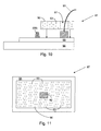
- Figures 10 and 11 illustrate another manner of using the preform.
- the diode is broadly designated at 87 and includes the substrate 54 and active portion 55 in a manner directly analogous to the embodiment illustrated in Figure 5 .
- the preform 90 carrying the phosphor particles 63 includes a cut out 91 that substantially matches an interior bond pad 92 on the active portion 55.
- the cutout 91 and the bond pad 92 are shaped and sized to register with one another so the preform can be pressed or otherwise placed on the bond pad 92.
- Figure 10 illustrates the bond pad 92 in square cross-section, but it will be understood that when taken in top plan view (e.g. Figure 11 ), the bond pad 92 could be circular, square, rectangular or some other appropriate shape.
- the raised border 56 can be optional because the registration between the interior bond pad 92 and the opening 91 in the preform 90 produces the intended positioning of the phosphor 63 with respect to the active portion 55.
- a wire 93 provides an electrical connection to the diode 87 in an otherwise conventional manner.
- the active portions 44 and 55 are typically formed from Group III nitride material system and emit in the blue portion of the visible spectrum.
- the phosphor 51 and 63 is typically cerium-doped YAG and emits predominantly in the yellow portion of the spectrum.
- the substrates 43 and 54 can again be selected from among silicon carbide, sapphire, and other sub-mounting structures.
- the resin pre-forms 50 and 62 respectively can be formed of any of the indicated (or other) relevant resin, with the polysiloxanes being particularly advantageous because of their stability with respect to high frequency blue emissions.
- Figure 6 is a schematic diagram of a diode precursor broadly designated at 65 illustrating some of the elements from Figures 3 , 4 and 5 in perspective fashion.
- the diode 65 includes the substrate 40 and two active layers illustrated at 66 and 67.
- the raised border 31 and the top surface 32 of the active portion formed by the epilayers 66 and 67 define a well 70 into which the droplet of phosphor-containing resin can be placed with the advantages just described.
- Figure 6 illustrates how a pre-form such as those illustrated in Figures 4 and 5 (50 and 62 respectively) can be supported on the raised border 31.
- the invention is a semiconductor precursor wafer. Aspects of this embodiment are illustrated in Figure 8 which is a schematic top plan view of a wafer broadly designated at 72.
- the wafer is not entirely circular, but includes one straight edge 74 referred to as the primary flat, and a second straight edge 75 referred to as the secondary flat.
- the straight edge of the primary flat is typically oriented so that the chord is parallel with a specified index crystal plane.
- the secondary flat is typically shorter than the primary flat and its position with respect to the primary flat identifies the face of the wafer.
- the wafer 72 includes a plurality of LED chip precursors 76 on the substrate 73.
- the individual LED chip precursors are illustrated as proportionally large rather than to actual scale. As in actual practice, some positions exist where flaws or defects prevent the completion of an LED precursor (or produce a defective precursor) and these are schematically represented by the empty positions.
- the chip precursors are typically formed of epitaxial layers of the light emitting semiconductor and potentially include some metal layers (for immediate or eventual electrical contact) and potentially some isolation structure for separating the individual diodes 76 from one another. These isolation structures can include edge trenches or deposited passivation materials, both of which are generally well understood in the art and will not be described in detail herein.
- a plurality, and preferably all, of the chip precursors 76 include the raised border described with respect to the individual chip embodiments.
- a plurality (and preferably all) of the bordered chip precursors are filled with the polymer resin and a plurality (and preferably all) of the resin filled chip precursors include a phosphor in the resin.
- the substrate is typically selected from among silicon carbide, sapphire and sub-mounting structures and the chips are formed from the Group III nitride material system.
- each chip precursor 76 contains the raised border, the invention provides some fabrication advantages over conventional techniques.
- each of the chip precursors 76 includes an identical composition of phosphor and an identical amount of the phosphor in the resin.
- different chip precursors can include different amounts of the phosphor, or different phosphor compositions, or different resin compositions, or combinations of these differences.
- the resins are selected from among the group consisting of PMMA, polycarbonate, polysiloxane, and polyester.
- the raised borders are again selected from the group consisting of metals, semiconductors and ceramics.
- the chip precursors emit in the blue portion of the spectrum and the phosphor down-converts the blue frequencies into predominantly yellow portions of the visible spectrum.
- the invention is a method that includes the steps of probing the wafer 72 that includes the plurality of LED precursor 76 to measure a quantity selected from the group consisting of wavelength, radiant flux, and combinations of these properties.
- the method then includes the step of creating a map of the probed wafer according to the measured quantity and adding an amount of phosphor in a resin to individual diodes on the wafer based upon the mapped output.
- the diodes can then be separated and sorted by output.
- the blue frequencies range from about 455 to about 490 nanometers within the visible spectrum.
- the emissions from individual diodes can differ from diode to diode across a single wafer.
- the probing step (the term “probing” being used generally rather than specifically) can be used to identify the different blue frequencies emitted by the individual diodes (or groups of diodes).
- the composition or amount (or both) of phosphor added to each individual diode can be tailored to that diode while the diode is still on the wafer to produce the desired light output.
- the wafer can also be probed and mapped according to color after the phosphor has been added to the diode precursors.
- the diodes can be mapped according to their blue emission before the phosphor is added, or they can be mapped according to their white emission after the phosphor has been added, or both.
- the phosphor can be added as a liquid droplet carrying the phosphor, as a pre-form.
- the invention comprises the method of forming the color conversion light emitting diode.
- the invention includes the steps of forming the raised border around the perimeter of the top surface of the diode chip and then filling the well created by the raised border with the polymer resin carrying the dispersed phosphor that is responsive to the frequencies emitted by the diode chip and that emits response to frequencies that are different from the frequencies emitted by the diode chip.
- the step of forming the raised border can be selected from among the steps of depositing a metal, a ceramic, or another semiconductor.
- the step of forming the raised border can comprise etching a silicon carbide substrate.
- the method comprises forming the raised border on a blue light emitting diode chip and filling the well with the polymer resin that carries a dispersed phosphor that emits predominantly in the yellow frequencies. If desired, the blue output of the chip can be measured at this point, following which the resin and phosphor are added in a combination that will produce a desired color coordinate of white light based upon the measured frequency output of the diode chip and the output of the phosphor.
- Figure 9 is a top plan view of another embodiment of a diode broadly designated at 80 according to the present invention.
- the raised border is formed of metal and is designated at 81. Wire bond pads for the diode form the corners 82.
- a number of current spreading fingers 83 and 84 are included within the well formed by the border 81 and the surface 85 of the active portion.
- This embodiment illustrates how the border can redirect low angle light to obtain greater quantum efficiency as well as illustrating a universal orientation for attaching the chip (because each side is identical). This also provides the ability to string multiple chips together in series or parallel, because in this embodiment, the raised border 81 can actually form part of the current spreading fingers.
Landscapes
- Led Device Packages (AREA)
- Led Devices (AREA)
Applications Claiming Priority (1)
| Application Number | Priority Date | Filing Date | Title |
|---|---|---|---|
| US11/775,958 US9401461B2 (en) | 2007-07-11 | 2007-07-11 | LED chip design for white conversion |
Publications (2)
| Publication Number | Publication Date |
|---|---|
| EP2015375A2 true EP2015375A2 (de) | 2009-01-14 |
| EP2015375A3 EP2015375A3 (de) | 2014-05-21 |
Family
ID=39874893
Family Applications (2)
| Application Number | Title | Priority Date | Filing Date |
|---|---|---|---|
| EP08160049.6A Active EP2015374B1 (de) | 2007-07-11 | 2008-07-09 | LED-Chipentwurf zur Weißumsetzung |
| EP08160051.2A Withdrawn EP2015375A3 (de) | 2007-07-11 | 2008-07-09 | Verfahren zur Einstellung einer Leuchtdiode mittels Ausgang |
Family Applications Before (1)
| Application Number | Title | Priority Date | Filing Date |
|---|---|---|---|
| EP08160049.6A Active EP2015374B1 (de) | 2007-07-11 | 2008-07-09 | LED-Chipentwurf zur Weißumsetzung |
Country Status (3)
| Country | Link |
|---|---|
| US (1) | US9401461B2 (de) |
| EP (2) | EP2015374B1 (de) |
| JP (1) | JP2009021599A (de) |
Families Citing this family (5)
| Publication number | Priority date | Publication date | Assignee | Title |
|---|---|---|---|---|
| KR100986336B1 (ko) * | 2009-10-22 | 2010-10-08 | 엘지이노텍 주식회사 | 발광소자, 발광소자 제조방법 및 발광소자 패키지 |
| CN102097425A (zh) * | 2009-12-09 | 2011-06-15 | 三星Led株式会社 | 发光二极管、制造磷光体层的方法和发光装置 |
| JP5486688B2 (ja) * | 2010-09-15 | 2014-05-07 | ライタイザー コリア カンパニー リミテッド | 発光ダイオード及びその製造方法 |
| KR101234166B1 (ko) * | 2011-06-20 | 2013-02-18 | 엘지이노텍 주식회사 | 광소자 패키지용 리플렉터 형성 방법 및 그 광소자 패키지 |
| KR101977278B1 (ko) * | 2012-10-29 | 2019-09-10 | 엘지이노텍 주식회사 | 발광 소자 |
Citations (2)
| Publication number | Priority date | Publication date | Assignee | Title |
|---|---|---|---|---|
| US3730707A (en) | 1967-04-17 | 1973-05-01 | Xerox Corp | Method of developing latent images |
| US20040080251A1 (en) * | 2002-10-29 | 2004-04-29 | Steranka Frank M. | Enhanced brightness light emitting device spot emitter |
Family Cites Families (120)
| Publication number | Priority date | Publication date | Assignee | Title |
|---|---|---|---|---|
| US4308114A (en) | 1980-07-21 | 1981-12-29 | Aluminum Company Of America | Electrolytic production of aluminum using a composite cathode |
| US4866005A (en) | 1987-10-26 | 1989-09-12 | North Carolina State University | Sublimation of silicon carbide to produce large, device quality single crystals of silicon carbide |
| US4902535A (en) | 1987-12-31 | 1990-02-20 | Air Products And Chemicals, Inc. | Method for depositing hard coatings on titanium or titanium alloys |
| US4946547A (en) | 1989-10-13 | 1990-08-07 | Cree Research, Inc. | Method of preparing silicon carbide surfaces for crystal growth |
| JPH0428269A (ja) | 1990-05-23 | 1992-01-30 | Fujikura Ltd | Ledベアチップの実装構造 |
| US5200022A (en) | 1990-10-03 | 1993-04-06 | Cree Research, Inc. | Method of improving mechanically prepared substrate surfaces of alpha silicon carbide for deposition of beta silicon carbide thereon and resulting product |
| JP3429921B2 (ja) | 1995-10-26 | 2003-07-28 | 三菱電機株式会社 | 半導体装置 |
| DE19638667C2 (de) | 1996-09-20 | 2001-05-17 | Osram Opto Semiconductors Gmbh | Mischfarbiges Licht abstrahlendes Halbleiterbauelement mit Lumineszenzkonversionselement |
| US5813753A (en) | 1997-05-27 | 1998-09-29 | Philips Electronics North America Corporation | UV/blue led-phosphor device with efficient conversion of UV/blues light to visible light |
| JP3257455B2 (ja) | 1997-07-17 | 2002-02-18 | 松下電器産業株式会社 | 発光装置 |
| DE19755734A1 (de) | 1997-12-15 | 1999-06-24 | Siemens Ag | Verfahren zur Herstellung eines oberflächenmontierbaren optoelektronischen Bauelementes |
| US6188230B1 (en) | 1997-12-16 | 2001-02-13 | Intel Corporation | Pickup chuck for double sided contact |
| US5959316A (en) | 1998-09-01 | 1999-09-28 | Hewlett-Packard Company | Multiple encapsulation of phosphor-LED devices |
| US6323480B1 (en) | 1999-01-28 | 2001-11-27 | Trw Inc. | Resonant photodetector |
| DE19918370B4 (de) | 1999-04-22 | 2006-06-08 | Osram Opto Semiconductors Gmbh | LED-Weißlichtquelle mit Linse |
| JP2000315823A (ja) | 1999-04-30 | 2000-11-14 | Runaraito Kk | 発光ダイオードおよびその製造方法 |
| EP1059668A3 (de) | 1999-06-09 | 2007-07-18 | Sanyo Electric Co., Ltd. | Integrierte Hybridschaltungsanordnung |
| DE19947044B9 (de) | 1999-09-30 | 2007-09-13 | Osram Opto Semiconductors Gmbh | Oberflächenmontierbares optoelektronisches Bauelement mit Reflektor und Verfahren zur Herstellung desselben |
| JP2001111109A (ja) * | 1999-10-07 | 2001-04-20 | Sharp Corp | 窒化ガリウム系化合物半導体発光素子 |
| US6483196B1 (en) | 2000-04-03 | 2002-11-19 | General Electric Company | Flip chip led apparatus |
| DE10020465A1 (de) | 2000-04-26 | 2001-11-08 | Osram Opto Semiconductors Gmbh | Strahlungsemittierendes Halbleiterbauelement mit Lumineszenzkonversionselement |
| US6577073B2 (en) | 2000-05-31 | 2003-06-10 | Matsushita Electric Industrial Co., Ltd. | Led lamp |
| JP4601128B2 (ja) | 2000-06-26 | 2010-12-22 | 株式会社光波 | Led光源およびその製造方法 |
| DE10033502A1 (de) | 2000-07-10 | 2002-01-31 | Osram Opto Semiconductors Gmbh | Optoelektronisches Modul, Verfahren zu dessen Herstellung und dessen Verwendung |
| US6747406B1 (en) | 2000-08-07 | 2004-06-08 | General Electric Company | LED cross-linkable phospor coating |
| US6635363B1 (en) | 2000-08-21 | 2003-10-21 | General Electric Company | Phosphor coating with self-adjusting distance from LED chip |
| US6650044B1 (en) | 2000-10-13 | 2003-11-18 | Lumileds Lighting U.S., Llc | Stenciling phosphor layers on light emitting diodes |
| US20020063520A1 (en) | 2000-11-29 | 2002-05-30 | Huei-Che Yu | Pre-formed fluorescent plate - LED device |
| JP2002166223A (ja) | 2000-11-30 | 2002-06-11 | Shimano Inc | 塗装部品 |
| US6671573B2 (en) * | 2000-12-14 | 2003-12-30 | Mitsubishi Denki Kabushiki Kaisha | Numerical controller and method for controlling the shaft of numeric controller |
| JP5110744B2 (ja) | 2000-12-21 | 2012-12-26 | フィリップス ルミレッズ ライティング カンパニー リミテッド ライアビリティ カンパニー | 発光装置及びその製造方法 |
| JP4184082B2 (ja) | 2001-01-03 | 2008-11-19 | ボシュ・アンド・ロム・インコーポレイテッド | 複数の薬剤を備えた徐放薬剤送達装置 |
| TW490863B (en) | 2001-02-12 | 2002-06-11 | Arima Optoelectronics Corp | Manufacturing method of LED with uniform color temperature |
| EP1246235A1 (de) | 2001-03-26 | 2002-10-02 | European Semiconductor Assembly (Eurasem) B.V. | Verfahren zum Einkapseln eines Chips mit empfindlicher Oberfläche |
| US6417019B1 (en) * | 2001-04-04 | 2002-07-09 | Lumileds Lighting, U.S., Llc | Phosphor converted light emitting diode |
| EP1386357A1 (de) | 2001-04-23 | 2004-02-04 | Plasma Ireland Limited | Beleuchtung |
| US6598998B2 (en) | 2001-05-04 | 2003-07-29 | Lumileds Lighting, U.S., Llc | Side emitting light emitting device |
| JP4122738B2 (ja) * | 2001-07-26 | 2008-07-23 | 松下電工株式会社 | 発光装置の製造方法 |
| PL373724A1 (en) | 2001-08-23 | 2005-09-05 | Yukiyasu Okumura | Color temperature-regulable led light |
| JP3948650B2 (ja) | 2001-10-09 | 2007-07-25 | アバゴ・テクノロジーズ・イーシービーユー・アイピー(シンガポール)プライベート・リミテッド | 発光ダイオード及びその製造方法 |
| US7858403B2 (en) | 2001-10-31 | 2010-12-28 | Cree, Inc. | Methods and systems for fabricating broad spectrum light emitting devices |
| KR100446290B1 (ko) | 2001-11-03 | 2004-09-01 | 삼성전자주식회사 | 댐을 포함하는 반도체 패키지 및 그 제조방법 |
| US6734465B1 (en) | 2001-11-19 | 2004-05-11 | Nanocrystals Technology Lp | Nanocrystalline based phosphors and photonic structures for solid state lighting |
| JP2003197973A (ja) | 2001-12-28 | 2003-07-11 | Toshiba Lighting & Technology Corp | 発光ダイオードおよびled表示装置 |
| JP3996408B2 (ja) * | 2002-02-28 | 2007-10-24 | ローム株式会社 | 半導体発光素子およびその製造方法 |
| JP3801931B2 (ja) | 2002-03-05 | 2006-07-26 | ローム株式会社 | Ledチップを使用した発光装置の構造及び製造方法 |
| JP4023723B2 (ja) | 2002-04-05 | 2007-12-19 | シチズン電子株式会社 | 表面実装型発光ダイオード |
| CA2427559A1 (en) | 2002-05-15 | 2003-11-15 | Sumitomo Electric Industries, Ltd. | White color light emitting device |
| JP2004015013A (ja) * | 2002-06-11 | 2004-01-15 | Toshiba Corp | 半導体発光素子、半導体発光素子の製造方法 |
| DE10237403B4 (de) | 2002-08-12 | 2004-07-29 | Infineon Technologies Ag | Opto-elektronisches Sende- und/oder Empfangsmodul und optischer Stecker |
| JP2004087812A (ja) | 2002-08-27 | 2004-03-18 | Sanyo Electric Co Ltd | 発光体 |
| US20060003477A1 (en) | 2002-10-30 | 2006-01-05 | Bert Braune | Method for producing a light source provided with electroluminescent diodes and comprising a luminescence conversion element |
| JP2004179343A (ja) | 2002-11-26 | 2004-06-24 | Matsushita Electric Works Ltd | 半導体基板とその製造方法 |
| US6917057B2 (en) | 2002-12-31 | 2005-07-12 | Gelcore Llc | Layered phosphor coatings for LED devices |
| JP3910171B2 (ja) | 2003-02-18 | 2007-04-25 | シャープ株式会社 | 半導体発光装置、その製造方法および電子撮像装置 |
| US6841934B2 (en) * | 2003-02-26 | 2005-01-11 | Harvatek Corporation | White light source from light emitting diode |
| JP4303550B2 (ja) | 2003-09-30 | 2009-07-29 | 豊田合成株式会社 | 発光装置 |
| JP4282346B2 (ja) | 2003-03-13 | 2009-06-17 | オリンパス株式会社 | 静電駆動装置及びその製造方法 |
| JP4274843B2 (ja) | 2003-04-21 | 2009-06-10 | シャープ株式会社 | Ledデバイスおよびそれを用いた携帯電話機器、デジタルカメラおよびlcd表示装置 |
| JP4374913B2 (ja) | 2003-06-05 | 2009-12-02 | 日亜化学工業株式会社 | 発光装置 |
| JP4239750B2 (ja) | 2003-08-13 | 2009-03-18 | セイコーエプソン株式会社 | マイクロレンズ及びマイクロレンズの製造方法、光学装置、光伝送装置、レーザプリンタ用ヘッド、並びにレーザプリンタ |
| JP4093943B2 (ja) * | 2003-09-30 | 2008-06-04 | 三洋電機株式会社 | 発光素子およびその製造方法 |
| US7427805B2 (en) | 2003-10-14 | 2008-09-23 | Shen Ming-Tung | Light-emitting diode chip package body and packaging method thereof |
| KR100587328B1 (ko) | 2003-10-16 | 2006-06-08 | 엘지전자 주식회사 | Led 면광원 |
| DE10351349A1 (de) * | 2003-10-31 | 2005-06-16 | Osram Opto Semiconductors Gmbh | Verfahren zum Hestellen eines Lumineszenzdiodenchips |
| US7321161B2 (en) | 2003-12-19 | 2008-01-22 | Philips Lumileds Lighting Company, Llc | LED package assembly with datum reference feature |
| US7189591B2 (en) * | 2003-12-19 | 2007-03-13 | Nitto Denko Corporation | Process for producing light-emitting semiconductor device |
| JP2005191420A (ja) | 2003-12-26 | 2005-07-14 | Stanley Electric Co Ltd | 波長変換層を有する半導体発光装置およびその製造方法 |
| WO2005078048A1 (en) | 2004-02-18 | 2005-08-25 | Showa Denko K.K. | Phosphor, production method thereof and light-emitting device using the phosphor |
| KR20050092300A (ko) | 2004-03-15 | 2005-09-21 | 삼성전기주식회사 | 고출력 발광 다이오드 패키지 |
| JP4504056B2 (ja) * | 2004-03-22 | 2010-07-14 | スタンレー電気株式会社 | 半導体発光装置の製造方法 |
| US20050211991A1 (en) * | 2004-03-26 | 2005-09-29 | Kyocera Corporation | Light-emitting apparatus and illuminating apparatus |
| US7517728B2 (en) | 2004-03-31 | 2009-04-14 | Cree, Inc. | Semiconductor light emitting devices including a luminescent conversion element |
| US7419912B2 (en) | 2004-04-01 | 2008-09-02 | Cree, Inc. | Laser patterning of light emitting devices |
| US20050280894A1 (en) | 2004-04-02 | 2005-12-22 | David Hartkop | Apparatus for creating a scanning-column backlight in a scanning aperture display device |
| US7868343B2 (en) | 2004-04-06 | 2011-01-11 | Cree, Inc. | Light-emitting devices having multiple encapsulation layers with at least one of the encapsulation layers including nanoparticles and methods of forming the same |
| DE102004021233A1 (de) * | 2004-04-30 | 2005-12-01 | Osram Opto Semiconductors Gmbh | Leuchtdiodenanordnung |
| TWI241034B (en) | 2004-05-20 | 2005-10-01 | Lighthouse Technology Co Ltd | Light emitting diode package |
| US7361938B2 (en) * | 2004-06-03 | 2008-04-22 | Philips Lumileds Lighting Company Llc | Luminescent ceramic for a light emitting device |
| US7148716B2 (en) | 2004-06-10 | 2006-12-12 | Texas Instruments Incorporated | System and method for the probing of a wafer |
| US20070295975A1 (en) | 2004-06-25 | 2007-12-27 | Sanyo Electric Co., Ltd. | Light-Emitting Device |
| US7534633B2 (en) | 2004-07-02 | 2009-05-19 | Cree, Inc. | LED with substrate modifications for enhanced light extraction and method of making same |
| US7497238B2 (en) | 2004-08-09 | 2009-03-03 | Alan Williams | Apparatus and method for cutting workpiece |
| KR100638611B1 (ko) | 2004-08-12 | 2006-10-26 | 삼성전기주식회사 | 다중 렌즈 발광 다이오드 |
| US8174037B2 (en) | 2004-09-22 | 2012-05-08 | Cree, Inc. | High efficiency group III nitride LED with lenticular surface |
| KR100674831B1 (ko) * | 2004-11-05 | 2007-01-25 | 삼성전기주식회사 | 백색 발광 다이오드 패키지 및 그 제조방법 |
| US7462502B2 (en) | 2004-11-12 | 2008-12-09 | Philips Lumileds Lighting Company, Llc | Color control by alteration of wavelength converting element |
| US7352011B2 (en) | 2004-11-15 | 2008-04-01 | Philips Lumileds Lighting Company, Llc | Wide emitting lens for LED useful for backlighting |
| US7404652B2 (en) * | 2004-12-15 | 2008-07-29 | Avago Technologies Ecbu Ip Pte Ltd | Light-emitting diode flash module with enhanced spectral emission |
| US7195944B2 (en) | 2005-01-11 | 2007-03-27 | Semileds Corporation | Systems and methods for producing white-light emitting diodes |
| TWI255566B (en) * | 2005-03-04 | 2006-05-21 | Jemitek Electronics Corp | Led |
| JP4739805B2 (ja) | 2005-04-22 | 2011-08-03 | スタンレー電気株式会社 | 光学特性制御ledデバイス及びその製造方法 |
| JP4692059B2 (ja) | 2005-04-25 | 2011-06-01 | パナソニック電工株式会社 | 発光装置の製造方法 |
| KR100665178B1 (ko) | 2005-05-26 | 2007-01-09 | 삼성전기주식회사 | 발광다이오드 패키지 제조방법 |
| JP4527025B2 (ja) | 2005-07-29 | 2010-08-18 | 本田技研工業株式会社 | 可変動弁装置を備える内燃機関 |
| US7646035B2 (en) | 2006-05-31 | 2010-01-12 | Cree, Inc. | Packaged light emitting devices including multiple index lenses and multiple index lenses for packaged light emitting devices |
| WO2007023411A1 (en) * | 2005-08-24 | 2007-03-01 | Philips Intellectual Property & Standards Gmbh | Light emitting diodes and lasers diodes with color converters |
| EP1922765B1 (de) * | 2005-08-24 | 2012-12-26 | Philips Intellectual Property & Standards GmbH | Elektrolumineszente vorrichtung mit einem lichtumwandlungselement |
| JP4945106B2 (ja) * | 2005-09-08 | 2012-06-06 | スタンレー電気株式会社 | 半導体発光装置 |
| US7344952B2 (en) | 2005-10-28 | 2008-03-18 | Philips Lumileds Lighting Company, Llc | Laminating encapsulant film containing phosphor over LEDs |
| US20070131940A1 (en) * | 2005-12-08 | 2007-06-14 | Unity Opto Technology Co., Ltd. | Color-mixing LED |
| US7795600B2 (en) | 2006-03-24 | 2010-09-14 | Goldeneye, Inc. | Wavelength conversion chip for use with light emitting diodes and method for making same |
| US7655957B2 (en) | 2006-04-27 | 2010-02-02 | Cree, Inc. | Submounts for semiconductor light emitting device packages and semiconductor light emitting device packages including the same |
| JP2007311445A (ja) | 2006-05-17 | 2007-11-29 | Stanley Electric Co Ltd | 半導体発光装置及びその製造方法 |
| TW200805694A (en) * | 2006-07-04 | 2008-01-16 | Secure Tech Co Ltd | Light-emitting component and manufacturing method thereof |
| US7910938B2 (en) | 2006-09-01 | 2011-03-22 | Cree, Inc. | Encapsulant profile for light emitting diodes |
| US7521862B2 (en) * | 2006-11-20 | 2009-04-21 | Philips Lumileds Lighting Co., Llc | Light emitting device including luminescent ceramic and light-scattering material |
| US7902564B2 (en) * | 2006-12-22 | 2011-03-08 | Koninklijke Philips Electronics N.V. | Multi-grain luminescent ceramics for light emitting devices |
| US8232564B2 (en) | 2007-01-22 | 2012-07-31 | Cree, Inc. | Wafer level phosphor coating technique for warm light emitting diodes |
| US9159888B2 (en) | 2007-01-22 | 2015-10-13 | Cree, Inc. | Wafer level phosphor coating method and devices fabricated utilizing method |
| US9024349B2 (en) | 2007-01-22 | 2015-05-05 | Cree, Inc. | Wafer level phosphor coating method and devices fabricated utilizing method |
| US10505083B2 (en) * | 2007-07-11 | 2019-12-10 | Cree, Inc. | Coating method utilizing phosphor containment structure and devices fabricated using same |
| US8866185B2 (en) | 2007-09-06 | 2014-10-21 | SemiLEDs Optoelectronics Co., Ltd. | White light LED with multiple encapsulation layers |
| US20090117672A1 (en) | 2007-10-01 | 2009-05-07 | Intematix Corporation | Light emitting devices with phosphor wavelength conversion and methods of fabrication thereof |
| US8783887B2 (en) | 2007-10-01 | 2014-07-22 | Intematix Corporation | Color tunable light emitting device |
| US8877524B2 (en) | 2008-03-31 | 2014-11-04 | Cree, Inc. | Emission tuning methods and devices fabricated utilizing methods |
| US7897419B2 (en) | 2008-12-23 | 2011-03-01 | Cree, Inc. | Color correction for wafer level white LEDs |
| US7804103B1 (en) | 2009-01-07 | 2010-09-28 | Lednovation, Inc. | White lighting device having short wavelength semiconductor die and trichromatic wavelength conversion layers |
| US7994531B2 (en) | 2009-04-02 | 2011-08-09 | Visera Technologies Company Limited | White-light light emitting diode chips and fabrication methods thereof |
| US8227274B2 (en) | 2010-01-26 | 2012-07-24 | Lightizer Korea Co. | Light emitting diode (LED) and method of manufacture |
-
2007
- 2007-07-11 US US11/775,958 patent/US9401461B2/en active Active
-
2008
- 2008-07-09 EP EP08160049.6A patent/EP2015374B1/de active Active
- 2008-07-09 EP EP08160051.2A patent/EP2015375A3/de not_active Withdrawn
- 2008-07-10 JP JP2008180814A patent/JP2009021599A/ja active Pending
Patent Citations (2)
| Publication number | Priority date | Publication date | Assignee | Title |
|---|---|---|---|---|
| US3730707A (en) | 1967-04-17 | 1973-05-01 | Xerox Corp | Method of developing latent images |
| US20040080251A1 (en) * | 2002-10-29 | 2004-04-29 | Steranka Frank M. | Enhanced brightness light emitting device spot emitter |
Non-Patent Citations (2)
| Title |
|---|
| SCHUBERT: "LIGHT-EMITTING DIODES", 2003, CAMBRIDGE UNIVERSITY PRESS |
| SZE: "PHYSICS OF SEMICONDUCTOR DEVICES", 1981 |
Also Published As
| Publication number | Publication date |
|---|---|
| US20090014731A1 (en) | 2009-01-15 |
| US9401461B2 (en) | 2016-07-26 |
| EP2015374B1 (de) | 2018-03-21 |
| EP2015374A2 (de) | 2009-01-14 |
| EP2015375A3 (de) | 2014-05-21 |
| EP2015374A3 (de) | 2014-05-21 |
| JP2009021599A (ja) | 2009-01-29 |
Similar Documents
| Publication | Publication Date | Title |
|---|---|---|
| CN102544267B (zh) | 一种晶片级荧光体涂层方法和利用该方法制造的器件 | |
| US7859000B2 (en) | LEDs using single crystalline phosphor and methods of fabricating same | |
| KR101548022B1 (ko) | 웨이퍼 레벨 형광체 코팅 방법 및 이 방법을 이용하여 제조된 소자 | |
| JP5918221B2 (ja) | Ledチップの製造方法 | |
| US10505083B2 (en) | Coating method utilizing phosphor containment structure and devices fabricated using same | |
| CN102334205B (zh) | 晶片级白色发光二极管的颜色校正 | |
| US9515229B2 (en) | Semiconductor light emitting devices with optical coatings and methods of making same | |
| TWI324834B (en) | Phosphor-converted led devices having improved light distribution uniformity | |
| US9391247B2 (en) | High power LEDs with non-polymer material lenses and methods of making the same | |
| TW201427105A (zh) | 波長轉換的發光裝置 | |
| EP2015374B1 (de) | LED-Chipentwurf zur Weißumsetzung | |
| TWI854189B (zh) | 用於發光二極體封裝的蓋結構中的光學配置和相關方法 | |
| KR102401828B1 (ko) | 발광소자 패키지 | |
| KR102523240B1 (ko) | 발광소자 패키지 | |
| US20240154076A1 (en) | Lumiphoric material structures for light-emitting diode packages and related methods |
Legal Events
| Date | Code | Title | Description |
|---|---|---|---|
| PUAI | Public reference made under article 153(3) epc to a published international application that has entered the european phase |
Free format text: ORIGINAL CODE: 0009012 |
|
| AK | Designated contracting states |
Kind code of ref document: A2 Designated state(s): AT BE BG CH CY CZ DE DK EE ES FI FR GB GR HR HU IE IS IT LI LT LU LV MC MT NL NO PL PT RO SE SI SK TR |
|
| AX | Request for extension of the european patent |
Extension state: AL BA MK RS |
|
| PUAL | Search report despatched |
Free format text: ORIGINAL CODE: 0009013 |
|
| AK | Designated contracting states |
Kind code of ref document: A3 Designated state(s): AT BE BG CH CY CZ DE DK EE ES FI FR GB GR HR HU IE IS IT LI LT LU LV MC MT NL NO PL PT RO SE SI SK TR |
|
| AX | Request for extension of the european patent |
Extension state: AL BA MK RS |
|
| RIC1 | Information provided on ipc code assigned before grant |
Ipc: H01L 33/00 20100101AFI20140416BHEP |
|
| 17P | Request for examination filed |
Effective date: 20141119 |
|
| RBV | Designated contracting states (corrected) |
Designated state(s): AT BE BG CH CY CZ DE DK EE ES FI FR GB GR HR HU IE IS IT LI LT LU LV MC MT NL NO PL PT RO SE SI SK TR |
|
| AKX | Designation fees paid |
Designated state(s): AT BE BG CH CY CZ DE DK EE ES FI FR GB GR HR HU IE IS IT LI LT LU LV MC MT NL NO PL PT RO SE SI SK TR |
|
| AXX | Extension fees paid |
Extension state: RS Extension state: MK Extension state: BA Extension state: AL |
|
| 17Q | First examination report despatched |
Effective date: 20160506 |
|
| STAA | Information on the status of an ep patent application or granted ep patent |
Free format text: STATUS: THE APPLICATION IS DEEMED TO BE WITHDRAWN |
|
| 18D | Application deemed to be withdrawn |
Effective date: 20160917 |