EP2011132B1 - Capacitive micro- electro- mechanical sensors with single crystal silicon electrodes - Google Patents
Capacitive micro- electro- mechanical sensors with single crystal silicon electrodes Download PDFInfo
- Publication number
- EP2011132B1 EP2011132B1 EP07755013.5A EP07755013A EP2011132B1 EP 2011132 B1 EP2011132 B1 EP 2011132B1 EP 07755013 A EP07755013 A EP 07755013A EP 2011132 B1 EP2011132 B1 EP 2011132B1
- Authority
- EP
- European Patent Office
- Prior art keywords
- layer
- electro
- crystal silicon
- capacitive micro
- electrode
- Prior art date
- Legal status (The legal status is an assumption and is not a legal conclusion. Google has not performed a legal analysis and makes no representation as to the accuracy of the status listed.)
- Active
Links
- 229910021421 monocrystalline silicon Inorganic materials 0.000 title claims description 23
- 239000000463 material Substances 0.000 claims description 6
- 239000003990 capacitor Substances 0.000 claims description 5
- 230000001133 acceleration Effects 0.000 claims description 4
- XUIMIQQOPSSXEZ-UHFFFAOYSA-N Silicon Chemical compound [Si] XUIMIQQOPSSXEZ-UHFFFAOYSA-N 0.000 description 13
- 239000002184 metal Substances 0.000 description 12
- 235000012431 wafers Nutrition 0.000 description 10
- 238000000034 method Methods 0.000 description 7
- 229910052710 silicon Inorganic materials 0.000 description 7
- 239000010703 silicon Substances 0.000 description 7
- 238000002955 isolation Methods 0.000 description 6
- 238000004519 manufacturing process Methods 0.000 description 6
- 229910021420 polycrystalline silicon Inorganic materials 0.000 description 5
- 229920005591 polysilicon Polymers 0.000 description 5
- 239000003989 dielectric material Substances 0.000 description 3
- 239000012528 membrane Substances 0.000 description 3
- VYPSYNLAJGMNEJ-UHFFFAOYSA-N Silicium dioxide Chemical compound O=[Si]=O VYPSYNLAJGMNEJ-UHFFFAOYSA-N 0.000 description 2
- 230000003647 oxidation Effects 0.000 description 2
- 238000007254 oxidation reaction Methods 0.000 description 2
- 238000000206 photolithography Methods 0.000 description 2
- 238000010276 construction Methods 0.000 description 1
- 230000009977 dual effect Effects 0.000 description 1
- 238000005530 etching Methods 0.000 description 1
- 230000004927 fusion Effects 0.000 description 1
- 230000010354 integration Effects 0.000 description 1
- 230000000873 masking effect Effects 0.000 description 1
- 238000012986 modification Methods 0.000 description 1
- 230000004048 modification Effects 0.000 description 1
- 238000007789 sealing Methods 0.000 description 1
- 239000004065 semiconductor Substances 0.000 description 1
- 235000012239 silicon dioxide Nutrition 0.000 description 1
- 239000000377 silicon dioxide Substances 0.000 description 1
- 238000004544 sputter deposition Methods 0.000 description 1
- 239000000758 substrate Substances 0.000 description 1
Images


Classifications
-
- G—PHYSICS
- G01—MEASURING; TESTING
- G01L—MEASURING FORCE, STRESS, TORQUE, WORK, MECHANICAL POWER, MECHANICAL EFFICIENCY, OR FLUID PRESSURE
- G01L9/00—Measuring steady of quasi-steady pressure of fluid or fluent solid material by electric or magnetic pressure-sensitive elements; Transmitting or indicating the displacement of mechanical pressure-sensitive elements, used to measure the steady or quasi-steady pressure of a fluid or fluent solid material, by electric or magnetic means
- G01L9/0041—Transmitting or indicating the displacement of flexible diaphragms
- G01L9/0072—Transmitting or indicating the displacement of flexible diaphragms using variations in capacitance
- G01L9/0073—Transmitting or indicating the displacement of flexible diaphragms using variations in capacitance using a semiconductive diaphragm
-
- B—PERFORMING OPERATIONS; TRANSPORTING
- B81—MICROSTRUCTURAL TECHNOLOGY
- B81B—MICROSTRUCTURAL DEVICES OR SYSTEMS, e.g. MICROMECHANICAL DEVICES
- B81B3/00—Devices comprising flexible or deformable elements, e.g. comprising elastic tongues or membranes
- B81B3/0018—Structures acting upon the moving or flexible element for transforming energy into mechanical movement or vice versa, i.e. actuators, sensors, generators
- B81B3/0021—Transducers for transforming electrical into mechanical energy or vice versa
-
- G—PHYSICS
- G01—MEASURING; TESTING
- G01P—MEASURING LINEAR OR ANGULAR SPEED, ACCELERATION, DECELERATION, OR SHOCK; INDICATING PRESENCE, ABSENCE, OR DIRECTION, OF MOVEMENT
- G01P15/00—Measuring acceleration; Measuring deceleration; Measuring shock, i.e. sudden change of acceleration
- G01P15/02—Measuring acceleration; Measuring deceleration; Measuring shock, i.e. sudden change of acceleration by making use of inertia forces using solid seismic masses
- G01P15/08—Measuring acceleration; Measuring deceleration; Measuring shock, i.e. sudden change of acceleration by making use of inertia forces using solid seismic masses with conversion into electric or magnetic values
- G01P15/0802—Details
-
- G—PHYSICS
- G01—MEASURING; TESTING
- G01P—MEASURING LINEAR OR ANGULAR SPEED, ACCELERATION, DECELERATION, OR SHOCK; INDICATING PRESENCE, ABSENCE, OR DIRECTION, OF MOVEMENT
- G01P15/00—Measuring acceleration; Measuring deceleration; Measuring shock, i.e. sudden change of acceleration
- G01P15/02—Measuring acceleration; Measuring deceleration; Measuring shock, i.e. sudden change of acceleration by making use of inertia forces using solid seismic masses
- G01P15/08—Measuring acceleration; Measuring deceleration; Measuring shock, i.e. sudden change of acceleration by making use of inertia forces using solid seismic masses with conversion into electric or magnetic values
- G01P15/125—Measuring acceleration; Measuring deceleration; Measuring shock, i.e. sudden change of acceleration by making use of inertia forces using solid seismic masses with conversion into electric or magnetic values by capacitive pick-up
-
- G—PHYSICS
- G01—MEASURING; TESTING
- G01P—MEASURING LINEAR OR ANGULAR SPEED, ACCELERATION, DECELERATION, OR SHOCK; INDICATING PRESENCE, ABSENCE, OR DIRECTION, OF MOVEMENT
- G01P15/00—Measuring acceleration; Measuring deceleration; Measuring shock, i.e. sudden change of acceleration
- G01P15/18—Measuring acceleration; Measuring deceleration; Measuring shock, i.e. sudden change of acceleration in two or more dimensions
-
- B—PERFORMING OPERATIONS; TRANSPORTING
- B81—MICROSTRUCTURAL TECHNOLOGY
- B81B—MICROSTRUCTURAL DEVICES OR SYSTEMS, e.g. MICROMECHANICAL DEVICES
- B81B2201/00—Specific applications of microelectromechanical systems
- B81B2201/02—Sensors
- B81B2201/0228—Inertial sensors
- B81B2201/0235—Accelerometers
-
- B—PERFORMING OPERATIONS; TRANSPORTING
- B81—MICROSTRUCTURAL TECHNOLOGY
- B81B—MICROSTRUCTURAL DEVICES OR SYSTEMS, e.g. MICROMECHANICAL DEVICES
- B81B2201/00—Specific applications of microelectromechanical systems
- B81B2201/02—Sensors
- B81B2201/0228—Inertial sensors
- B81B2201/0242—Gyroscopes
-
- B—PERFORMING OPERATIONS; TRANSPORTING
- B81—MICROSTRUCTURAL TECHNOLOGY
- B81B—MICROSTRUCTURAL DEVICES OR SYSTEMS, e.g. MICROMECHANICAL DEVICES
- B81B2201/00—Specific applications of microelectromechanical systems
- B81B2201/02—Sensors
- B81B2201/0264—Pressure sensors
-
- G—PHYSICS
- G01—MEASURING; TESTING
- G01P—MEASURING LINEAR OR ANGULAR SPEED, ACCELERATION, DECELERATION, OR SHOCK; INDICATING PRESENCE, ABSENCE, OR DIRECTION, OF MOVEMENT
- G01P15/00—Measuring acceleration; Measuring deceleration; Measuring shock, i.e. sudden change of acceleration
- G01P15/02—Measuring acceleration; Measuring deceleration; Measuring shock, i.e. sudden change of acceleration by making use of inertia forces using solid seismic masses
- G01P15/08—Measuring acceleration; Measuring deceleration; Measuring shock, i.e. sudden change of acceleration by making use of inertia forces using solid seismic masses with conversion into electric or magnetic values
- G01P2015/0805—Measuring acceleration; Measuring deceleration; Measuring shock, i.e. sudden change of acceleration by making use of inertia forces using solid seismic masses with conversion into electric or magnetic values being provided with a particular type of spring-mass-system for defining the displacement of a seismic mass due to an external acceleration
- G01P2015/0808—Measuring acceleration; Measuring deceleration; Measuring shock, i.e. sudden change of acceleration by making use of inertia forces using solid seismic masses with conversion into electric or magnetic values being provided with a particular type of spring-mass-system for defining the displacement of a seismic mass due to an external acceleration for defining in-plane movement of the mass, i.e. movement of the mass in the plane of the substrate
- G01P2015/0811—Measuring acceleration; Measuring deceleration; Measuring shock, i.e. sudden change of acceleration by making use of inertia forces using solid seismic masses with conversion into electric or magnetic values being provided with a particular type of spring-mass-system for defining the displacement of a seismic mass due to an external acceleration for defining in-plane movement of the mass, i.e. movement of the mass in the plane of the substrate for one single degree of freedom of movement of the mass
- G01P2015/0814—Measuring acceleration; Measuring deceleration; Measuring shock, i.e. sudden change of acceleration by making use of inertia forces using solid seismic masses with conversion into electric or magnetic values being provided with a particular type of spring-mass-system for defining the displacement of a seismic mass due to an external acceleration for defining in-plane movement of the mass, i.e. movement of the mass in the plane of the substrate for one single degree of freedom of movement of the mass for translational movement of the mass, e.g. shuttle type
-
- G—PHYSICS
- G01—MEASURING; TESTING
- G01P—MEASURING LINEAR OR ANGULAR SPEED, ACCELERATION, DECELERATION, OR SHOCK; INDICATING PRESENCE, ABSENCE, OR DIRECTION, OF MOVEMENT
- G01P15/00—Measuring acceleration; Measuring deceleration; Measuring shock, i.e. sudden change of acceleration
- G01P15/02—Measuring acceleration; Measuring deceleration; Measuring shock, i.e. sudden change of acceleration by making use of inertia forces using solid seismic masses
- G01P15/08—Measuring acceleration; Measuring deceleration; Measuring shock, i.e. sudden change of acceleration by making use of inertia forces using solid seismic masses with conversion into electric or magnetic values
- G01P2015/0805—Measuring acceleration; Measuring deceleration; Measuring shock, i.e. sudden change of acceleration by making use of inertia forces using solid seismic masses with conversion into electric or magnetic values being provided with a particular type of spring-mass-system for defining the displacement of a seismic mass due to an external acceleration
- G01P2015/0822—Measuring acceleration; Measuring deceleration; Measuring shock, i.e. sudden change of acceleration by making use of inertia forces using solid seismic masses with conversion into electric or magnetic values being provided with a particular type of spring-mass-system for defining the displacement of a seismic mass due to an external acceleration for defining out-of-plane movement of the mass
- G01P2015/0825—Measuring acceleration; Measuring deceleration; Measuring shock, i.e. sudden change of acceleration by making use of inertia forces using solid seismic masses with conversion into electric or magnetic values being provided with a particular type of spring-mass-system for defining the displacement of a seismic mass due to an external acceleration for defining out-of-plane movement of the mass for one single degree of freedom of movement of the mass
- G01P2015/0831—Measuring acceleration; Measuring deceleration; Measuring shock, i.e. sudden change of acceleration by making use of inertia forces using solid seismic masses with conversion into electric or magnetic values being provided with a particular type of spring-mass-system for defining the displacement of a seismic mass due to an external acceleration for defining out-of-plane movement of the mass for one single degree of freedom of movement of the mass the mass being of the paddle type having the pivot axis between the longitudinal ends of the mass, e.g. see-saw configuration
-
- G—PHYSICS
- G01—MEASURING; TESTING
- G01P—MEASURING LINEAR OR ANGULAR SPEED, ACCELERATION, DECELERATION, OR SHOCK; INDICATING PRESENCE, ABSENCE, OR DIRECTION, OF MOVEMENT
- G01P15/00—Measuring acceleration; Measuring deceleration; Measuring shock, i.e. sudden change of acceleration
- G01P15/02—Measuring acceleration; Measuring deceleration; Measuring shock, i.e. sudden change of acceleration by making use of inertia forces using solid seismic masses
- G01P15/08—Measuring acceleration; Measuring deceleration; Measuring shock, i.e. sudden change of acceleration by making use of inertia forces using solid seismic masses with conversion into electric or magnetic values
- G01P2015/0805—Measuring acceleration; Measuring deceleration; Measuring shock, i.e. sudden change of acceleration by making use of inertia forces using solid seismic masses with conversion into electric or magnetic values being provided with a particular type of spring-mass-system for defining the displacement of a seismic mass due to an external acceleration
- G01P2015/0822—Measuring acceleration; Measuring deceleration; Measuring shock, i.e. sudden change of acceleration by making use of inertia forces using solid seismic masses with conversion into electric or magnetic values being provided with a particular type of spring-mass-system for defining the displacement of a seismic mass due to an external acceleration for defining out-of-plane movement of the mass
- G01P2015/084—Measuring acceleration; Measuring deceleration; Measuring shock, i.e. sudden change of acceleration by making use of inertia forces using solid seismic masses with conversion into electric or magnetic values being provided with a particular type of spring-mass-system for defining the displacement of a seismic mass due to an external acceleration for defining out-of-plane movement of the mass the mass being suspended at more than one of its sides, e.g. membrane-type suspension, so as to permit multi-axis movement of the mass
-
- H—ELECTRICITY
- H01—ELECTRIC ELEMENTS
- H01L—SEMICONDUCTOR DEVICES NOT COVERED BY CLASS H10
- H01L28/00—Passive two-terminal components without a potential-jump or surface barrier for integrated circuits; Details thereof; Multistep manufacturing processes therefor
- H01L28/40—Capacitors
Definitions
- the present invention relates generally to sensors. More particularly, the present invention relates to capacitive micro-electro-mechanical sensors with single crystal silicon electrodes.
- FR 2 722 878 discloses a capacitive differential pressure sensor on a micromachined semiconductor substrate.
- the sensor includes two plates attached to the top and bottom surfaces of an intermediate silicon membrane.
- the two plates are made of silicon while their links to the membrane are made of silicon dioxide.
- the pressures to be measured are transmitted to either side of the membrane via openings provided in the top and bottom plates.
- the present invention provides capacitive micro-electro-mechanical sensors having single crystal silicon electrodes, according to claim 1.
- the sensors preferably sense at least; one of pressure, acceleration, angular rate or resonance.
- the sensors include two layers.
- the first layer is made of single-crystal silicon and has a top surface and a bottom surface.
- the first layer forms at least one electrode.
- the second layer is also made of single crystal silicon and has a top surface and a bottom surface.
- At least one electrode is defined in the second layer by an insulating trench of dielectrical material that extends from the top surface to the bottom surface of the layer. This insulating trench forms a periphery around this electrode.
- the second layer further includes at least one electrical guard, wherein the at least one electrical guard is defined by a second insulating trench of dielectrical material that extends from the top surface to the bottom surface of the second layer.
- the at least one electrode in the first layer and the at least one electrode in the second layer together define a capacitor.
- the top surface of the second layer is etched to form a cavity, which forms the capacitive gap.
- the sensor further includes at least one electrical contact situated on the bottom surface of the second layer. This electrical contact is in electrical connection with the at least one electrode in the second layer.
- the first layer forms a diaphragm.
- the first layer may also be etched to define a resonant structure, spring, or proof mass.
- the senor further includes a third single crystal silicon layer, which is separated from the top surface of the top layer by a dielectric layer. In one embodiment, this third layer is etched to define a pressure port. In this embodiment, the sensor senses pressure, with the advantage that the pressure port is on the opposite side of the device from the electrical contacts..
- FIG. 1A shows a cross-sectional view of a capacitive micro-electromechanical sensor according to the present invention.
- the sensor includes a first layer 110, with top surface 112 and bottom surface 114.
- First layer 110 is made of single crystal silicon and contains at least one electrode 130.
- the sensor further includes a second layer 120, with a top surface 122 and a bottom surface 124.
- Second layer 120 contains an isolating trench 150 made of dielectrical material that extends from top surface 122 to bottom surface 124. Isolating trench 150 defines electrode 140.
- Electrode 140 is electrically connected to electrical contact 160, such as a wire-bond pad.
- first layer 110 contains all of the sensing elements of the sensor, such that the sensing elements are on the opposite side of the sensor to electrical contact 160 .
- Electrodes 130 and 140 together define a capacitor, with capacitive gap 170.
- Capacitive gap 170 is preferably formed in second layer 120 to allow precise spatial definition of gap 170.
- FIG. 1B shows a plan view of the bottom surface 124 of second layer 120.
- FIG. 1B shows that isolating trench 150 forms a periphery around electrode 140 in order to define electrode 140. While a square trench is shown in the figure, trench 150 may be of any geometry.
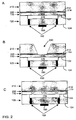
- FIG. 2 shows several embodiments of a sensor according to the present invention.
- FIG. 2A shows a sensor having a third single crystal silicon layer 210, which is separated from top surface 112 of first layer 110 by a dielectric layer 220.
- first layer 110 has been thinned to form a diaphragm 130.
- third layer 230 is etched to form a pressure port 230 ( FIG. 2B ).
- first layer 110 may be etched to define, for example, a proof mass 260, springs 250, or a resonant structure (not shown).
- First layer 110 may be released for device movement by etch removal of dielectric layer 220. ( FIG. 2C ).
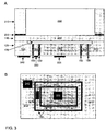
- FIG. 3A shows a cross-sectional view of a preferred pressure sensor according to the present invention.
- the pressure sensor has a first single crystal silicon layer 110, which has been milled or etched to form diaphragm 130. Diaphragm 130 serves as a first electrode in a capacitor.
- the pressure sensor also has a second single crystal silicon layer 120, which has been etched to form a cavity 170.
- Second single crystal silicon layer 120 includes two isolating trenches 150. Isolating trenches 150 define a stationary electrode 340, which forms the second electrode of the capacitor; an electrical guard 360; and a driven common port 370.
- Stationary electrode 340, electrical guard 360 and driven common port 370 are electrically connected to metal bond pads 320, 330, and 340, respectively.
- the pressure sensor also has a third single crystal silicon layer 210, which is separated from diaphragm 130 by dielectric layer 220.
- Layer 220 may be, for example, a buried oxide layer.
- Layer 210 is etched to form a pressure port 230. Notice in this sensor that single crystal silicon is used at all key pressure points, no metal is needed within the sensor, and the pressure port is situated opposite to the sensitive metal bond pads.
- FIG. 3B shows a planar view of this pressure sensor from the bottom surface of the sensor.
- Isolation trenches 150 can be seen to define stationary electrode 340, electrical guard 360, and common drive port 370. These electronic components are in electrical connection with metal bond pads 320, 330, and 340, respectively.
- FIG. 4A shows a cross-sectional view
- FIG. 4B shows a plan view of a preferred accelerometer according to the present invention.
- the accelerometer is built in the same die as the pressure sensor described in FIG. 3 .
- the accelerometer has a first single crystal silicon layer 110, which has been etched to form trenches 430 and accelerometer shuttle 420.
- the sensor also has a second silicon layer 120, which has been etched to form a cavity 170.
- Second single crystal silicon layer 120 includes isolating trenches 150 which define a common drive port 460 and four electrodes, 440, 442, 444, and 450.
- the common drive port 460 and four electrodes 440, 442, 444, and 450 are electrically connected to metal bond pads 490, 470, 480, 492, and 494, respectively.
- the accelerometer also has a third single crystal silicon layer 210, which is separated from first layer 130 by dielectric layer 220.
- Layer 220 may be, for example, a buried oxide layer.
- Layer 220 is etched to give gap 410 for the accelerometer shuttle 420. While the accelerometer shown is a dual axis accelerometer that measures in plane acceleration and out of plane acceleration, a third axis in plane is easy to achieve by duplicating and rotating the accelerometer 90 degrees about its out of plane axis
- FIG. 5A shows a plan view and FIG. 5B shows an isometric view of accelerometer shuttle 420.
- Finger electrodes 510, isolated support 515, lateral springs 520, lateral spring ends 525, rotational springs 530, proof mass 540, gimbal frame 550, and isolation trenches 560 are shown.
- Finger electrodes 510 are attached to an isolated support 515 which would connect to either electrode 442 or 444. All of these structures are created through etching of first layer 120, as described below.
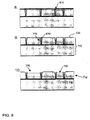
- Steps 1-17, shown in FIGS. 6-10 are schematic depictions of an example of manufacturing process steps for making a sensor according to the present invention.
- Steps 1-3 are used for processing a SOI wafer
- steps 4-10 are used for processing isolation trenches
- steps 11-17 are dual-wafer processing steps.
- the steps show a method of simultaneously fabricating a pressure sensor along with an accelerometer according to the invention.
- a sensor that senses only pressure sensor could be built by eliminating steps 2 and 3.
- Modifications to the following steps can be made to create other types of sensors according to the present invention.
- polysilicon layers can be added and patterned similar to surface micromaching. Adding these layers to layer 612 allows for these layers to be inside the cavity 730 and not interfere with the bonding surfaces 910
- Step 1 forms an oxide 620 on a SOI wafer 610 by oxidation.
- SOI wafer 610's thinner active layer 612 eventually forms a diaphragm, such as diaphragm 130 in FIG 2B .
- Layer 612 is relatively highly doped between about 0.1 to 0.01 Ohms/cm to be used as a conductive electrode surface.
- the thicker handle layer 614 forms third layer 210 depicted in FIG. 2 .
- Step 2 patterns and etches the oxide 620 through photolithography and wet oxide etch to give openings 630 in the oxide 620, such that the underlying silicon 612 can be etched in step 3.
- Step 3 is a Deep Reactive Ion Etch (DRIE) etch to form springs 650, etch holes 640, fingers 510, isolation trenches 560, proof mass 550, rotational springs 530 and other structures in the diaphragm layer 612 (See FIG. 5 ).
- DRIE Deep Reactive Ion Etch
- Other types of sensors such as an angular rate sensor, resonator, or shear sensor could be made in this layer by changing the masking artwork to incorporate other geometries typical of what can be made in a surface micromachined process.
- multiple types of sensors can be made simultaneously, therefore allowing higher integration levels on one chip.
- a resonant structure can be made simply by defining a proof mass, spring and comb drive / comb sense combination as recognized by those skilled in the art.
- Step 4 forms an oxide 720, again through oxidation, on a new SOI wafer 710 containing an active layer 712 of relatively highly doped silicon, which forms isolation trenches defining single crystal silicon electrodes, such as 340, 350, and 370 shown in FIG. 3 , and a handle wafer 714, which is etched off or ground and polished off later in the sequence.
- Step 5 is to etch the oxide 720 in a RIE oxide etcher to form openings 730 in oxide 720.
- active layer 712 is DRIE etched from openings 730, stopping on the Box layer 716, forming trenches 740.
- step 7 trenches 740 are oxidized with thermal oxide growth to provide dielectric material 750, which will define and isolate the single crystal silicon electrodes.
- step 8 the trenches 740 are filled with polysilicon 810. This reduces the amount of dielectric material required to form the isolation trenches. The entire trench can be filled with dielectric material but it is found to be expensive and difficult if thermal oxide is used because of the requited thickness of the oxide.
- Step 9 is a polysilicon blanket etch of wafer 710, using any type of etcher including a DRIE, RIE or even a barrel etcher, to remove the polysilicon 810 from the surface of wafer 710, stopping on oxide 720 and leaving polysilicon 810 only on the inside of the remaining trench 740.
- a DRIE etch of silicon layer 712 in step 10 of approximately 0.5 to 2 microns depth forms cavities 730, such as cavity 170 in FIG. 2 .
- Oxide 620 and 720 is removed from surfaces 910 in step 11 using a wet etch such as BOE. This allows surfaces 910 to be aligned and bonded in step 12 using high temperature wafer bonding techniques.
- Step 11 also allows the proof mass to be released by undercutting the Box layer 616 and forming gap 920, such as gap 410 in FIG. 4 .
- openings 920 are etched in the top oxide 620 using BOE and bottom oxide 720 is removed. This allows silicon layer 614 to be etched in step 14 by DRIE etch creating port 1010, such as port 230 in FIG. 2B .
- handle wafer 714 is removed through backgrind and polish or through DRIE etch or RIE etch or a barrel etcher.
- Step 15 etches Box 616 and Box 716 by using a RIE oxide etch, exposing diaphragm 612 and interconnects 1020, respectively.
- metal 1030 is deposited using a sputtering system in step 16. Metal 1030 is etched in step 17 using photolithography and wet etch to form interconnects 1020 and metal bond pads 1040, such as bond pad 160 in FIG. 2 .
Applications Claiming Priority (3)
| Application Number | Priority Date | Filing Date | Title |
|---|---|---|---|
| US79179006P | 2006-04-13 | 2006-04-13 | |
| US11/707,347 US7539003B2 (en) | 2005-12-01 | 2007-02-16 | Capacitive micro-electro-mechanical sensors with single crystal silicon electrodes |
| PCT/US2007/008599 WO2007120576A2 (en) | 2006-04-13 | 2007-04-04 | Capacitive micro- electro-mechanical sensors with single crystal silicon electrodes |
Publications (3)
| Publication Number | Publication Date |
|---|---|
| EP2011132A2 EP2011132A2 (en) | 2009-01-07 |
| EP2011132A4 EP2011132A4 (en) | 2014-07-16 |
| EP2011132B1 true EP2011132B1 (en) | 2016-06-29 |
Family
ID=38610099
Family Applications (1)
| Application Number | Title | Priority Date | Filing Date |
|---|---|---|---|
| EP07755013.5A Active EP2011132B1 (en) | 2006-04-13 | 2007-04-04 | Capacitive micro- electro- mechanical sensors with single crystal silicon electrodes |
Country Status (5)
| Country | Link |
|---|---|
| US (1) | US7539003B2 (ja) |
| EP (1) | EP2011132B1 (ja) |
| JP (3) | JP5331678B2 (ja) |
| CN (1) | CN101449347B (ja) |
| WO (1) | WO2007120576A2 (ja) |
Families Citing this family (52)
| Publication number | Priority date | Publication date | Assignee | Title |
|---|---|---|---|---|
| US7741964B2 (en) * | 2007-05-31 | 2010-06-22 | Schrader Electronics Ltd. | Tire pressure detector having reduced power consumption mechanism |
| JP5260155B2 (ja) * | 2008-06-16 | 2013-08-14 | 株式会社堀場エステック | 静電容量型圧力センサ及びその製造方法 |
| US8238073B2 (en) * | 2008-07-18 | 2012-08-07 | Synaptics, Inc. | In-molded capacitive sensors |
| US8499629B2 (en) * | 2008-10-10 | 2013-08-06 | Honeywell International Inc. | Mounting system for torsional suspension of a MEMS device |
| ITBO20080079U1 (it) * | 2008-10-30 | 2010-04-30 | Lorenzo Peretto | Sistema costruttivo per un sensore capacitivo. |
| US8739626B2 (en) * | 2009-08-04 | 2014-06-03 | Fairchild Semiconductor Corporation | Micromachined inertial sensor devices |
| US8421168B2 (en) * | 2009-11-17 | 2013-04-16 | Fairchild Semiconductor Corporation | Microelectromechanical systems microphone packaging systems |
| US8490495B2 (en) | 2010-05-05 | 2013-07-23 | Consensic, Inc. | Capacitive pressure sensor with vertical electrical feedthroughs and method to make the same |
| DE112011103124T5 (de) | 2010-09-18 | 2013-12-19 | Fairchild Semiconductor Corporation | Biegelager zum Verringern von Quadratur für mitschwingende mikromechanische Vorrichtungen |
| US8813564B2 (en) | 2010-09-18 | 2014-08-26 | Fairchild Semiconductor Corporation | MEMS multi-axis gyroscope with central suspension and gimbal structure |
| EP2616389B1 (en) | 2010-09-18 | 2017-04-05 | Fairchild Semiconductor Corporation | Multi-die mems package |
| EP2616772B1 (en) | 2010-09-18 | 2016-06-22 | Fairchild Semiconductor Corporation | Micromachined monolithic 3-axis gyroscope with single drive |
| US9278846B2 (en) | 2010-09-18 | 2016-03-08 | Fairchild Semiconductor Corporation | Micromachined monolithic 6-axis inertial sensor |
| US9856132B2 (en) | 2010-09-18 | 2018-01-02 | Fairchild Semiconductor Corporation | Sealed packaging for microelectromechanical systems |
| KR101332701B1 (ko) | 2010-09-20 | 2013-11-25 | 페어차일드 세미컨덕터 코포레이션 | 기준 커패시터를 포함하는 미소 전자기계 압력 센서 |
| KR101311966B1 (ko) | 2010-09-20 | 2013-10-14 | 페어차일드 세미컨덕터 코포레이션 | 감소된 션트 커패시턴스를 갖는 관통 실리콘 비아 |
| JP5649474B2 (ja) * | 2011-01-26 | 2015-01-07 | ローム株式会社 | 静電容量型圧力センサおよび静電容量型圧力センサの製造方法 |
| US8673756B2 (en) * | 2011-04-14 | 2014-03-18 | Robert Bosch Gmbh | Out-of-plane spacer defined electrode |
| JP5833752B2 (ja) * | 2011-06-29 | 2015-12-16 | インベンセンス, インク.Invensense, Inc. | 一部が縦型集積電子回路とともに環境に曝露された密閉封止型memsデバイス |
| US9062972B2 (en) | 2012-01-31 | 2015-06-23 | Fairchild Semiconductor Corporation | MEMS multi-axis accelerometer electrode structure |
| US8978475B2 (en) | 2012-02-01 | 2015-03-17 | Fairchild Semiconductor Corporation | MEMS proof mass with split z-axis portions |
| US8714021B2 (en) | 2012-02-27 | 2014-05-06 | Amphenol Thermometrics, Inc. | Catheter die and method of fabricating the same |
| US8857264B2 (en) | 2012-03-30 | 2014-10-14 | Amphenol Thermometrics, Inc. | Catheter die |
| US8754694B2 (en) | 2012-04-03 | 2014-06-17 | Fairchild Semiconductor Corporation | Accurate ninety-degree phase shifter |
| US8742964B2 (en) | 2012-04-04 | 2014-06-03 | Fairchild Semiconductor Corporation | Noise reduction method with chopping for a merged MEMS accelerometer sensor |
| US9488693B2 (en) | 2012-04-04 | 2016-11-08 | Fairchild Semiconductor Corporation | Self test of MEMS accelerometer with ASICS integrated capacitors |
| US9069006B2 (en) | 2012-04-05 | 2015-06-30 | Fairchild Semiconductor Corporation | Self test of MEMS gyroscope with ASICs integrated capacitors |
| EP2647955B8 (en) | 2012-04-05 | 2018-12-19 | Fairchild Semiconductor Corporation | MEMS device quadrature phase shift cancellation |
| KR102058489B1 (ko) | 2012-04-05 | 2019-12-23 | 페어차일드 세미컨덕터 코포레이션 | 멤스 장치 프론트 엔드 전하 증폭기 |
| EP2647952B1 (en) | 2012-04-05 | 2017-11-15 | Fairchild Semiconductor Corporation | Mems device automatic-gain control loop for mechanical amplitude drive |
| KR101999745B1 (ko) | 2012-04-12 | 2019-10-01 | 페어차일드 세미컨덕터 코포레이션 | 미세 전자 기계 시스템 구동기 |
| US9625272B2 (en) | 2012-04-12 | 2017-04-18 | Fairchild Semiconductor Corporation | MEMS quadrature cancellation and signal demodulation |
| DE102013014881B4 (de) | 2012-09-12 | 2023-05-04 | Fairchild Semiconductor Corporation | Verbesserte Silizium-Durchkontaktierung mit einer Füllung aus mehreren Materialien |
| EP2725334B1 (en) * | 2012-10-25 | 2020-04-15 | Invensense, Inc. | A pressure sensor having a membrane and a method for fabricating the same |
| US9156676B2 (en) * | 2013-04-09 | 2015-10-13 | Honeywell International Inc. | Sensor with isolated diaphragm |
| US9837935B2 (en) | 2013-10-29 | 2017-12-05 | Honeywell International Inc. | All-silicon electrode capacitive transducer on a glass substrate |
| EP3367082A1 (en) * | 2013-11-06 | 2018-08-29 | Invensense, Inc. | Pressure sensor |
| EP2871455B1 (en) | 2013-11-06 | 2020-03-04 | Invensense, Inc. | Pressure sensor |
| CN103552980A (zh) * | 2013-11-15 | 2014-02-05 | 安徽北方芯动联科微系统技术有限公司 | Mems芯片圆片级封装方法及其单片超小型mems芯片 |
| US9464950B2 (en) * | 2013-11-15 | 2016-10-11 | Rosemount Aerospace Inc. | Capacitive pressure sensors for high temperature applications |
| NO2777050T3 (ja) * | 2014-02-25 | 2018-06-16 | ||
| FI126599B (en) | 2014-02-26 | 2017-03-15 | Murata Manufacturing Co | Microelectromechanical frame structure |
| CN105084296B (zh) * | 2014-04-25 | 2017-02-08 | 无锡华润上华半导体有限公司 | Mems电容式压力传感器的制作方法 |
| EP3614115A1 (en) | 2015-04-02 | 2020-02-26 | InvenSense, Inc. | Pressure sensor |
| US10697994B2 (en) | 2017-02-22 | 2020-06-30 | Semiconductor Components Industries, Llc | Accelerometer techniques to compensate package stress |
| KR101988469B1 (ko) * | 2017-07-26 | 2019-06-13 | 주식회사 신성씨앤티 | 멤스 센서 및 그 제조 방법 |
| CN108051134A (zh) * | 2017-11-23 | 2018-05-18 | 胡波 | 闭环工作方式的电容式压力传感器 |
| CN108680138A (zh) * | 2018-05-09 | 2018-10-19 | 中交第公路勘察设计研究院有限公司 | 软土地基路基大变形沉降自动监测系统及其方法 |
| DE102018119943A1 (de) * | 2018-08-16 | 2020-02-20 | Endress+Hauser SE+Co. KG | Drucksensor |
| US11225409B2 (en) | 2018-09-17 | 2022-01-18 | Invensense, Inc. | Sensor with integrated heater |
| US11060929B2 (en) * | 2019-03-04 | 2021-07-13 | Silicon Microstructures, Inc. | Pressure sensor die attach |
| CN113785178A (zh) * | 2019-05-17 | 2021-12-10 | 应美盛股份有限公司 | 气密性改进的压力传感器 |
Family Cites Families (30)
| Publication number | Priority date | Publication date | Assignee | Title |
|---|---|---|---|---|
| US4617606A (en) * | 1985-01-31 | 1986-10-14 | Motorola, Inc. | Capacitive pressure transducer |
| JPS61272623A (ja) * | 1985-05-29 | 1986-12-02 | Fuji Electric Co Ltd | 静電容量式圧力センサ |
| JPS6259828A (ja) * | 1985-09-11 | 1987-03-16 | Fuji Electric Co Ltd | 静電容量式圧力センサ |
| FI78784C (fi) * | 1988-01-18 | 1989-09-11 | Vaisala Oy | Tryckgivarkonstruktion och foerfarande foer framstaellning daerav. |
| DE4106288C2 (de) * | 1991-02-28 | 2001-05-31 | Bosch Gmbh Robert | Sensor zur Messung von Drücken oder Beschleunigungen |
| JPH06323939A (ja) * | 1993-05-17 | 1994-11-25 | Omron Corp | 静電容量式センサ |
| US5511428A (en) | 1994-06-10 | 1996-04-30 | Massachusetts Institute Of Technology | Backside contact of sensor microstructures |
| FR2722878B1 (fr) | 1994-07-22 | 1996-09-06 | Suisse Electronique Microtech | Capteur de pression differentielle de type capacitif |
| JPH08122251A (ja) * | 1994-10-19 | 1996-05-17 | Mitsubishi Materials Corp | 赤外線式ガス分析装置 |
| US6212056B1 (en) | 1999-03-26 | 2001-04-03 | Lucent Technologies Inc. | Micromachined variable capacitor |
| JP3588286B2 (ja) | 1999-10-06 | 2004-11-10 | 株式会社山武 | 容量式圧力センサ |
| US6396677B1 (en) * | 2000-05-17 | 2002-05-28 | Xerox Corporation | Photolithographically-patterned variable capacitor structures and method of making |
| JP3629185B2 (ja) * | 2000-06-15 | 2005-03-16 | 株式会社日立製作所 | 半導体センサ及びその製造方法 |
| US6507475B1 (en) * | 2000-06-27 | 2003-01-14 | Motorola, Inc. | Capacitive device and method of manufacture |
| US6377438B1 (en) * | 2000-10-23 | 2002-04-23 | Mcnc | Hybrid microelectromechanical system tunable capacitor and associated fabrication methods |
| JP2002228678A (ja) * | 2001-02-02 | 2002-08-14 | Denso Corp | 半導体力学量センサとその製造方法 |
| US20020167072A1 (en) | 2001-03-16 | 2002-11-14 | Andosca Robert George | Electrostatically actuated micro-electro-mechanical devices and method of manufacture |
| JP2002328137A (ja) * | 2001-04-27 | 2002-11-15 | Matsushita Electric Works Ltd | 加速度センサ及びその製造方法 |
| WO2002096166A1 (en) * | 2001-05-18 | 2002-11-28 | Corporation For National Research Initiatives | Radio frequency microelectromechanical systems (mems) devices on low-temperature co-fired ceramic (ltcc) substrates |
| US6909589B2 (en) * | 2002-11-20 | 2005-06-21 | Corporation For National Research Initiatives | MEMS-based variable capacitor |
| JP4159895B2 (ja) | 2003-02-17 | 2008-10-01 | キヤノンアネルバ株式会社 | 静電容量型圧力センサ及びその製造方法 |
| US6928879B2 (en) * | 2003-02-26 | 2005-08-16 | Robert Bosch Gmbh | Episeal pressure sensor and method for making an episeal pressure sensor |
| SE526366C3 (sv) * | 2003-03-21 | 2005-10-26 | Silex Microsystems Ab | Elektriska anslutningar i substrat |
| JP2004356708A (ja) * | 2003-05-27 | 2004-12-16 | Hosiden Corp | 音響検出機構及びその製造方法 |
| US6930368B2 (en) | 2003-07-31 | 2005-08-16 | Hewlett-Packard Development Company, L.P. | MEMS having a three-wafer structure |
| US7111518B1 (en) | 2003-09-19 | 2006-09-26 | Silicon Microstructures, Inc. | Extremely low cost pressure sensor realized using deep reactive ion etching |
| US20050172717A1 (en) | 2004-02-06 | 2005-08-11 | General Electric Company | Micromechanical device with thinned cantilever structure and related methods |
| JP2005233877A (ja) | 2004-02-23 | 2005-09-02 | Alps Electric Co Ltd | 圧力センサ |
| CN1314969C (zh) * | 2004-04-29 | 2007-05-09 | 中国科学院上海微系统与信息技术研究所 | 一种单硅片体微机械工艺实现的带静电自检测的加速度计 |
| US7272954B2 (en) * | 2004-07-14 | 2007-09-25 | L'air Liquide, Societe Anonyme A Directoire Et Conseil De Surveillance Pour L'etude Et L'exploitation Des Proceded Georges Claude | Low temperature air separation process for producing pressurized gaseous product |
-
2007
- 2007-02-16 US US11/707,347 patent/US7539003B2/en active Active
- 2007-04-04 EP EP07755013.5A patent/EP2011132B1/en active Active
- 2007-04-04 WO PCT/US2007/008599 patent/WO2007120576A2/en active Application Filing
- 2007-04-04 CN CN2007800178712A patent/CN101449347B/zh active Active
- 2007-04-04 JP JP2009505402A patent/JP5331678B2/ja active Active
-
2013
- 2013-04-26 JP JP2013093834A patent/JP5806254B2/ja active Active
-
2015
- 2015-05-07 JP JP2015095070A patent/JP5956644B2/ja active Active
Also Published As
| Publication number | Publication date |
|---|---|
| WO2007120576A2 (en) | 2007-10-25 |
| JP5956644B2 (ja) | 2016-07-27 |
| US20070279832A1 (en) | 2007-12-06 |
| CN101449347A (zh) | 2009-06-03 |
| JP5806254B2 (ja) | 2015-11-10 |
| EP2011132A2 (en) | 2009-01-07 |
| JP2015180521A (ja) | 2015-10-15 |
| CN101449347B (zh) | 2013-07-17 |
| JP2013198979A (ja) | 2013-10-03 |
| JP2009533866A (ja) | 2009-09-17 |
| US7539003B2 (en) | 2009-05-26 |
| WO2007120576A3 (en) | 2008-10-30 |
| EP2011132A4 (en) | 2014-07-16 |
| JP5331678B2 (ja) | 2013-10-30 |
Similar Documents
| Publication | Publication Date | Title |
|---|---|---|
| EP2011132B1 (en) | Capacitive micro- electro- mechanical sensors with single crystal silicon electrodes | |
| EP3052901B1 (en) | Inertial and pressure sensors on single chip | |
| KR101332701B1 (ko) | 기준 커패시터를 포함하는 미소 전자기계 압력 센서 | |
| US7247246B2 (en) | Vertical integration of a MEMS structure with electronics in a hermetically sealed cavity | |
| KR102217083B1 (ko) | 압력 센서 | |
| US7104129B2 (en) | Vertically integrated MEMS structure with electronics in a hermetically sealed cavity | |
| CN100579892C (zh) | 微型机电系统元件及其制造方法 | |
| EP2423157A2 (en) | MEMS pressure sensor device and method of fabricating same | |
| US9194882B2 (en) | Inertial and pressure sensors on single chip | |
| JP2004505269A (ja) | マイクロマシン化された絶対圧センサ | |
| JP2006247833A (ja) | Mems素子パッケージ及びその製造方法 | |
| US10407301B2 (en) | MEMS device including a capacitive pressure sensor and manufacturing process thereof | |
| US6794271B2 (en) | Method for fabricating a microelectromechanical system (MEMS) device using a pre-patterned bridge | |
| KR100661350B1 (ko) | Mems 소자 패키지 및 그 제조방법 | |
| KR20010074906A (ko) | 마이크로 기계 부품 및 그의 제조 방법 | |
| US20230061430A1 (en) | Method for manufacturing an integrated system including a capacitive pressure sensor and an inertial sensor, and integrated system | |
| JP2011038780A (ja) | 半導体装置及び半導体装置の製造方法 | |
| WO2010107618A2 (en) | Method of accurately spacing z-axis electrode | |
| CN115752815A (zh) | 制造包括电容压力传感器和惯性传感器的集成系统的方法及集成系统 | |
| Wiemer et al. | WAFERBONDING F OR PATTERNING OF MICROMECHANICAL SENSORS |
Legal Events
| Date | Code | Title | Description |
|---|---|---|---|
| PUAI | Public reference made under article 153(3) epc to a published international application that has entered the european phase |
Free format text: ORIGINAL CODE: 0009012 |
|
| AK | Designated contracting states |
Kind code of ref document: A2 Designated state(s): AT BE BG CH CY CZ DE DK EE ES FI FR GB GR HU IE IS IT LI LT LU LV MC MT NL PL PT RO SE SI SK TR |
|
| AX | Request for extension of the european patent |
Extension state: AL BA HR MK RS |
|
| RIN1 | Information on inventor provided before grant (corrected) |
Inventor name: BRYZEK, JANUSZ Inventor name: RAY, CURTIS, A. |
|
| 17P | Request for examination filed |
Effective date: 20090430 |
|
| RBV | Designated contracting states (corrected) |
Designated state(s): AT BE BG CH CY CZ DE DK EE ES FI FR GB GR HU IE IS IT LI LT LU LV MC MT NL PL PT RO SE SI SK TR |
|
| DAX | Request for extension of the european patent (deleted) | ||
| RAP1 | Party data changed (applicant data changed or rights of an application transferred) |
Owner name: SAMSUNG ELECTRONICS CO., LTD. |
|
| A4 | Supplementary search report drawn up and despatched |
Effective date: 20140616 |
|
| RIC1 | Information provided on ipc code assigned before grant |
Ipc: B81B 3/00 20060101AFI20140610BHEP |
|
| REG | Reference to a national code |
Ref country code: DE Ref legal event code: R079 Ref document number: 602007046813 Country of ref document: DE Free format text: PREVIOUS MAIN CLASS: H01G0005000000 Ipc: B81B0003000000 |
|
| GRAP | Despatch of communication of intention to grant a patent |
Free format text: ORIGINAL CODE: EPIDOSNIGR1 |
|
| RIC1 | Information provided on ipc code assigned before grant |
Ipc: G01L 9/00 20060101ALI20151214BHEP Ipc: B81B 3/00 20060101AFI20151214BHEP Ipc: G01P 15/125 20060101ALI20151214BHEP |
|
| INTG | Intention to grant announced |
Effective date: 20160107 |
|
| GRAS | Grant fee paid |
Free format text: ORIGINAL CODE: EPIDOSNIGR3 |
|
| GRAA | (expected) grant |
Free format text: ORIGINAL CODE: 0009210 |
|
| AK | Designated contracting states |
Kind code of ref document: B1 Designated state(s): AT BE BG CH CY CZ DE DK EE ES FI FR GB GR HU IE IS IT LI LT LU LV MC MT NL PL PT RO SE SI SK TR |
|
| REG | Reference to a national code |
Ref country code: GB Ref legal event code: FG4D |
|
| REG | Reference to a national code |
Ref country code: CH Ref legal event code: EP |
|
| REG | Reference to a national code |
Ref country code: AT Ref legal event code: REF Ref document number: 808942 Country of ref document: AT Kind code of ref document: T Effective date: 20160715 |
|
| REG | Reference to a national code |
Ref country code: IE Ref legal event code: FG4D |
|
| REG | Reference to a national code |
Ref country code: DE Ref legal event code: R096 Ref document number: 602007046813 Country of ref document: DE |
|
| REG | Reference to a national code |
Ref country code: LT Ref legal event code: MG4D |
|
| PG25 | Lapsed in a contracting state [announced via postgrant information from national office to epo] |
Ref country code: LT Free format text: LAPSE BECAUSE OF FAILURE TO SUBMIT A TRANSLATION OF THE DESCRIPTION OR TO PAY THE FEE WITHIN THE PRESCRIBED TIME-LIMIT Effective date: 20160629 Ref country code: FI Free format text: LAPSE BECAUSE OF FAILURE TO SUBMIT A TRANSLATION OF THE DESCRIPTION OR TO PAY THE FEE WITHIN THE PRESCRIBED TIME-LIMIT Effective date: 20160629 |
|
| REG | Reference to a national code |
Ref country code: NL Ref legal event code: MP Effective date: 20160629 |
|
| PG25 | Lapsed in a contracting state [announced via postgrant information from national office to epo] |
Ref country code: GR Free format text: LAPSE BECAUSE OF FAILURE TO SUBMIT A TRANSLATION OF THE DESCRIPTION OR TO PAY THE FEE WITHIN THE PRESCRIBED TIME-LIMIT Effective date: 20160930 Ref country code: LV Free format text: LAPSE BECAUSE OF FAILURE TO SUBMIT A TRANSLATION OF THE DESCRIPTION OR TO PAY THE FEE WITHIN THE PRESCRIBED TIME-LIMIT Effective date: 20160629 Ref country code: NL Free format text: LAPSE BECAUSE OF FAILURE TO SUBMIT A TRANSLATION OF THE DESCRIPTION OR TO PAY THE FEE WITHIN THE PRESCRIBED TIME-LIMIT Effective date: 20160629 Ref country code: SE Free format text: LAPSE BECAUSE OF FAILURE TO SUBMIT A TRANSLATION OF THE DESCRIPTION OR TO PAY THE FEE WITHIN THE PRESCRIBED TIME-LIMIT Effective date: 20160629 |
|
| REG | Reference to a national code |
Ref country code: AT Ref legal event code: MK05 Ref document number: 808942 Country of ref document: AT Kind code of ref document: T Effective date: 20160629 |
|
| PG25 | Lapsed in a contracting state [announced via postgrant information from national office to epo] |
Ref country code: SK Free format text: LAPSE BECAUSE OF FAILURE TO SUBMIT A TRANSLATION OF THE DESCRIPTION OR TO PAY THE FEE WITHIN THE PRESCRIBED TIME-LIMIT Effective date: 20160629 Ref country code: IS Free format text: LAPSE BECAUSE OF FAILURE TO SUBMIT A TRANSLATION OF THE DESCRIPTION OR TO PAY THE FEE WITHIN THE PRESCRIBED TIME-LIMIT Effective date: 20161029 Ref country code: RO Free format text: LAPSE BECAUSE OF FAILURE TO SUBMIT A TRANSLATION OF THE DESCRIPTION OR TO PAY THE FEE WITHIN THE PRESCRIBED TIME-LIMIT Effective date: 20160629 Ref country code: EE Free format text: LAPSE BECAUSE OF FAILURE TO SUBMIT A TRANSLATION OF THE DESCRIPTION OR TO PAY THE FEE WITHIN THE PRESCRIBED TIME-LIMIT Effective date: 20160629 Ref country code: CZ Free format text: LAPSE BECAUSE OF FAILURE TO SUBMIT A TRANSLATION OF THE DESCRIPTION OR TO PAY THE FEE WITHIN THE PRESCRIBED TIME-LIMIT Effective date: 20160629 Ref country code: IT Free format text: LAPSE BECAUSE OF FAILURE TO SUBMIT A TRANSLATION OF THE DESCRIPTION OR TO PAY THE FEE WITHIN THE PRESCRIBED TIME-LIMIT Effective date: 20160629 |
|
| PG25 | Lapsed in a contracting state [announced via postgrant information from national office to epo] |
Ref country code: ES Free format text: LAPSE BECAUSE OF FAILURE TO SUBMIT A TRANSLATION OF THE DESCRIPTION OR TO PAY THE FEE WITHIN THE PRESCRIBED TIME-LIMIT Effective date: 20160629 Ref country code: BE Free format text: LAPSE BECAUSE OF FAILURE TO SUBMIT A TRANSLATION OF THE DESCRIPTION OR TO PAY THE FEE WITHIN THE PRESCRIBED TIME-LIMIT Effective date: 20160629 Ref country code: PL Free format text: LAPSE BECAUSE OF FAILURE TO SUBMIT A TRANSLATION OF THE DESCRIPTION OR TO PAY THE FEE WITHIN THE PRESCRIBED TIME-LIMIT Effective date: 20160629 Ref country code: PT Free format text: LAPSE BECAUSE OF FAILURE TO SUBMIT A TRANSLATION OF THE DESCRIPTION OR TO PAY THE FEE WITHIN THE PRESCRIBED TIME-LIMIT Effective date: 20161031 Ref country code: AT Free format text: LAPSE BECAUSE OF FAILURE TO SUBMIT A TRANSLATION OF THE DESCRIPTION OR TO PAY THE FEE WITHIN THE PRESCRIBED TIME-LIMIT Effective date: 20160629 |
|
| REG | Reference to a national code |
Ref country code: FR Ref legal event code: PLFP Year of fee payment: 11 |
|
| REG | Reference to a national code |
Ref country code: DE Ref legal event code: R097 Ref document number: 602007046813 Country of ref document: DE |
|
| PLBE | No opposition filed within time limit |
Free format text: ORIGINAL CODE: 0009261 |
|
| STAA | Information on the status of an ep patent application or granted ep patent |
Free format text: STATUS: NO OPPOSITION FILED WITHIN TIME LIMIT |
|
| PG25 | Lapsed in a contracting state [announced via postgrant information from national office to epo] |
Ref country code: DK Free format text: LAPSE BECAUSE OF FAILURE TO SUBMIT A TRANSLATION OF THE DESCRIPTION OR TO PAY THE FEE WITHIN THE PRESCRIBED TIME-LIMIT Effective date: 20160629 |
|
| 26N | No opposition filed |
Effective date: 20170330 |
|
| STAA | Information on the status of an ep patent application or granted ep patent |
Free format text: STATUS: NO OPPOSITION FILED WITHIN TIME LIMIT |
|
| PG25 | Lapsed in a contracting state [announced via postgrant information from national office to epo] |
Ref country code: SI Free format text: LAPSE BECAUSE OF FAILURE TO SUBMIT A TRANSLATION OF THE DESCRIPTION OR TO PAY THE FEE WITHIN THE PRESCRIBED TIME-LIMIT Effective date: 20160629 Ref country code: BG Free format text: LAPSE BECAUSE OF FAILURE TO SUBMIT A TRANSLATION OF THE DESCRIPTION OR TO PAY THE FEE WITHIN THE PRESCRIBED TIME-LIMIT Effective date: 20160929 |
|
| REG | Reference to a national code |
Ref country code: CH Ref legal event code: PL |
|
| REG | Reference to a national code |
Ref country code: IE Ref legal event code: MM4A |
|
| PG25 | Lapsed in a contracting state [announced via postgrant information from national office to epo] |
Ref country code: MC Free format text: LAPSE BECAUSE OF FAILURE TO SUBMIT A TRANSLATION OF THE DESCRIPTION OR TO PAY THE FEE WITHIN THE PRESCRIBED TIME-LIMIT Effective date: 20160629 |
|
| PG25 | Lapsed in a contracting state [announced via postgrant information from national office to epo] |
Ref country code: CH Free format text: LAPSE BECAUSE OF NON-PAYMENT OF DUE FEES Effective date: 20170430 Ref country code: LU Free format text: LAPSE BECAUSE OF NON-PAYMENT OF DUE FEES Effective date: 20170404 Ref country code: LI Free format text: LAPSE BECAUSE OF NON-PAYMENT OF DUE FEES Effective date: 20170430 |
|
| REG | Reference to a national code |
Ref country code: FR Ref legal event code: PLFP Year of fee payment: 12 |
|
| PG25 | Lapsed in a contracting state [announced via postgrant information from national office to epo] |
Ref country code: IE Free format text: LAPSE BECAUSE OF NON-PAYMENT OF DUE FEES Effective date: 20170404 |
|
| PG25 | Lapsed in a contracting state [announced via postgrant information from national office to epo] |
Ref country code: MT Free format text: LAPSE BECAUSE OF NON-PAYMENT OF DUE FEES Effective date: 20170404 |
|
| PG25 | Lapsed in a contracting state [announced via postgrant information from national office to epo] |
Ref country code: HU Free format text: LAPSE BECAUSE OF FAILURE TO SUBMIT A TRANSLATION OF THE DESCRIPTION OR TO PAY THE FEE WITHIN THE PRESCRIBED TIME-LIMIT; INVALID AB INITIO Effective date: 20070404 |
|
| PG25 | Lapsed in a contracting state [announced via postgrant information from national office to epo] |
Ref country code: CY Free format text: LAPSE BECAUSE OF NON-PAYMENT OF DUE FEES Effective date: 20160629 |
|
| PG25 | Lapsed in a contracting state [announced via postgrant information from national office to epo] |
Ref country code: TR Free format text: LAPSE BECAUSE OF FAILURE TO SUBMIT A TRANSLATION OF THE DESCRIPTION OR TO PAY THE FEE WITHIN THE PRESCRIBED TIME-LIMIT Effective date: 20160629 |
|
| PGFP | Annual fee paid to national office [announced via postgrant information from national office to epo] |
Ref country code: FR Payment date: 20230328 Year of fee payment: 17 |
|
| P01 | Opt-out of the competence of the unified patent court (upc) registered |
Effective date: 20230520 |
|
| PGFP | Annual fee paid to national office [announced via postgrant information from national office to epo] |
Ref country code: DE Payment date: 20230321 Year of fee payment: 17 |
|
| PGFP | Annual fee paid to national office [announced via postgrant information from national office to epo] |
Ref country code: GB Payment date: 20240321 Year of fee payment: 18 |