EP1990725B1 - Zentrale verarbeitungseinheit, steuerverfahren für eine zentrale verarbeitungseinheit und informationsverarbeitungssystem - Google Patents
Zentrale verarbeitungseinheit, steuerverfahren für eine zentrale verarbeitungseinheit und informationsverarbeitungssystem Download PDFInfo
- Publication number
- EP1990725B1 EP1990725B1 EP06714786.8A EP06714786A EP1990725B1 EP 1990725 B1 EP1990725 B1 EP 1990725B1 EP 06714786 A EP06714786 A EP 06714786A EP 1990725 B1 EP1990725 B1 EP 1990725B1
- Authority
- EP
- European Patent Office
- Prior art keywords
- central processing
- memory
- processing apparatus
- buses
- system controller
- Prior art date
- Legal status (The legal status is an assumption and is not a legal conclusion. Google has not performed a legal analysis and makes no representation as to the accuracy of the status listed.)
- Expired - Fee Related
Links
Images


Classifications
-
- G—PHYSICS
- G06—COMPUTING; CALCULATING OR COUNTING
- G06F—ELECTRIC DIGITAL DATA PROCESSING
- G06F12/00—Accessing, addressing or allocating within memory systems or architectures
- G06F12/02—Addressing or allocation; Relocation
- G06F12/06—Addressing a physical block of locations, e.g. base addressing, module addressing, memory dedication
- G06F12/0607—Interleaved addressing
-
- G—PHYSICS
- G06—COMPUTING; CALCULATING OR COUNTING
- G06F—ELECTRIC DIGITAL DATA PROCESSING
- G06F13/00—Interconnection of, or transfer of information or other signals between, memories, input/output devices or central processing units
- G06F13/14—Handling requests for interconnection or transfer
- G06F13/16—Handling requests for interconnection or transfer for access to memory bus
- G06F13/1605—Handling requests for interconnection or transfer for access to memory bus based on arbitration
- G06F13/1647—Handling requests for interconnection or transfer for access to memory bus based on arbitration with interleaved bank access
Definitions
- the present invention relates to a central processing apparatus, a control method therefore, and an information processing system.
- a calculation capability of each central processing apparatus i.e., central processing unit (CPU) chip
- CPU central processing unit
- a single system controller is connected to a central processing apparatus so that the system controller carries out an interleaving to distribute access requests to a plurality of memory media. Therefore, the conventional technique cannot enable the central processing apparatus to recognize that the interleaving is taking place.
- EP0164138A1 discloses a CPU that communicates with various devices on a system bus and communicates with two further groups of devices by way of two interfaces and corresponding buses whose timing and control characteristics are different from each other and from those of the system bus.
- US2005/138276A1 discloses an apparatus and method to perform high-speed memory read accesses on dynamic random access memories ("DRAMs") for read-intensive memory applications. It is disclosed that at least one input/output (“I/O") channel of a memory controller is coupled to a pair of DRAM chips via a common address/control bus and via two independent data busses. Each DRAM chip may include multiple internal memory banks.
- DRAMs dynamic random access memories
- the present invention discloses that a plurality of buses (i.e., WAYS) are furnished between a central processing apparatus and a plurality of system controllers so as to make the central processing apparatus carry out an interleaving, and thereby the number of signal lines connected to the individual system controllers is reduced.
- WAYS a plurality of buses
- Some technical problems are caused by connecting a plurality of buses to a central processing apparatus and making the central processing apparatus carry out a direct interleaving.
- the central processing apparatus is required to issue an input/output (I/O) request packet to an appropriate bus on which an I/O device exists, in accordance with the present I/O device to be desirably accessed.
- I/O input/output
- a main storage is interleaved by using an address and therefore it is possible to implement a conversion process for obtaining the number of the system controller (i.e., the bus) to which the memory as the target of access (“access target” memory) is connected relatively easily from the address.
- the system controller i.e., the bus
- each of the plurality of central processing apparatuses must have setup information of the same content, bringing about the problem of substantially wasting the storage resource within the central processing apparatus and of ushering in an increased cost thereof.
- the present invention is contrived to overcome these technical problems in the following manner.
- a purpose of the present invention is to enable an effective utilization of the processing capability of a central processing apparatus without complicating the configuration of a system controller connected to the central processing apparatus.
- Another purpose of the present invention aims at achieving an improvement in processing capability by a central processing apparatus performing a low-cost interleaving without complicating the configuration within the central processing apparatus and/or the management thereof.
- a first aspect of the present invention is to provide a central processing apparatus comprising a bus control unit for performing input/output of information between a plurality of buses connected to a system controller; a memory access control unit for distributing memory access requests to a plurality of the buses in accordance with memory addresses; and an input/output access control unit for accessing an external input/output device by way of the bus, wherein the input/output access control unit carries out a first step of inquiring, to said system controller by way of a specific one of the plurality of buses, as to which of the plurality of buses the input/output device of an access target exists on, and a second step of accessing the input/output device by using the bus which is response from the system controller.
- Another aspect of the present invention is to provide the central processing apparatus according to the first aspect, wherein the memory access control unit performs a memory interleave for parallelly accessing, in accordance with the memory addresses, a plurality of memory media individually connected to a plurality of the buses.
- Another aspect of the present invention is to provide a control method used for a central processing apparatus, comprising the steps of: connecting the central processing apparatus to a plurality of buses connected to a system controller; and the central processing apparatus carrying out a memory interleave for distributing a plurality of memory access requests to memory media existing on the buses in accordance with memory addresses, further comprising the steps of: the central processing apparatus inquiring, to said system controller by way of a specific one of the plurality of buses, as to which of the plurality of buses the input/output device of an access target exists on; and the central processing apparatus accessing the input/output device by using the bus which is responded from a system controller.
- Another aspect of the present invention is to provide an information processing system, comprising: a central processing apparatus; a plurality of system controllers, each of which is connected to either a memory medium or an input/output device under the control of the system controller; a plurality of buses connecting the central processing apparatus and individual system controllers, respectively; and a memory access control unit that is equipped in the central processing apparatus and which distributes a plurality of memory access requests to memory media existing on the bus in accordance with memory addresses, wherein the central processing apparatus further comprises an input/output access control unit for carrying out a first step of inquiring, to a specific system controller by way of a specific one of the plurality of buses, as to which of the plurality of buses the input/output device of an access target exists on, and a second step of accessing the input/output device by using the bus that was returned in the response from the system controller.
- Another aspect of the present invention is to provide the information processing system according to the sixth aspect, wherein each of a plurality of central processing apparatuses is respectively
- Another aspect of the present invention is to provide the information processing system according to the sixth aspect, wherein each of the system controllers is constituted by a plurality of semiconductor chips.
- the present invention is contrived to connect a plurality of buses to the central processing apparatus so that the central processing apparatus executes a memory interleave and therefore a thick bus having an unnecessarily large number of signal lines is not required between the central processing apparatus and system controller.
- This contrivance makes it possible to attain a high memory bandwidth while reducing the production cost of semiconductor chips and the like constituting the system controller, and to cause the central processing apparatus to exert the processing capability sufficiently.
- the present invention is contrived to confirm which bus a target input/output device exists on by way of a specific bus and then carry out an input/output access to the input/output bus that was returned in the response when accessing an input/output device, thereby eliminating the need to equip each of a plurality of central processing apparatuses with a special storage resource for setting common configuration information and, furthermore, the need to carry out a cumbersome operation for managing the consistency of the aforementioned configuration information.
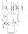
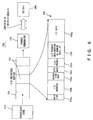
- Fig. 1 is a conceptual diagram exemplifying the configuration of an information processing system comprising a central processing apparatus according to a preferred embodiment of the present invention.
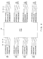
- Fig. 2 is a conceptual diagram exemplifying the connection state of a bus to a central processing apparatus according to the present embodiment.
- the information processing system comprises a plurality of CPU nodes 100, a plurality of system controllers 300, a plurality of memory media 400, and a plurality of I/O devices 500, as exemplified in Fig. 1 .
- the memory media 400 and I/O devices 500 are connected to, and under the control of, each system controller 300.
- Each system controller 300 controls the exchanges between each CPU node 100 and the memory medium 400 and I/O device 500, the latter two of which are under the control of the system controller 300.
- the I/O device 500 is mapped in a memory address space so that an access from the CPU node 100 to the I/O device 500 is carried out by way of a memory-mapped I/O.
- the SC0 representing a plurality of system controllers 300 (i.e., SC0 through SC3) comprises a configuration management table 310 for setting information describing which of the system controllers 300 (i.e., system buses 200) a plurality of I/O devices 500 exist under the control of.
- the SC0 refers to the configuration management table 310, and makes a response in response to a later described inquiry from the CPU node 100.
- the memory medium 400 comprises, for example, storage media (i.e., memory banks) such as semiconductor memory and a memory controller controlling them.
- the memory media 400 existing under the control of individual system controllers 300 are physically independent from each other and are enabled for parallel access operations.
- the present embodiment is configured to connect the individual system controllers 300 (i.e., SC0 through SC3) to each of a plurality of CPU nodes 100 by way of system buses 200.
- the individual CPU node 100 comprises the function of executing a memory interleave for distributing memory access requests to a plurality of system buses 200 (i.e., system controllers 300) and thereby carrying out parallel memory accesses among the plurality of memory media 400 under the control of individual system controllers 300, as described later.
- system buses 200 i.e., system controllers 300
- the present embodiment is configured to control a memory interleave for accesses to the memory media 400 at the level of the CPU nodes 100.
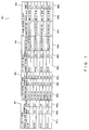
- system buses 200 equipped between an individual CPU node 100 and each of the plurality of system controllers 300 comprises an SC request bus 210 (SCREQ_BUSn) and an SC order bus 220 (SCODR_BUSn).
- SC request bus 210 SCREQ_BUSn
- SC order bus 220 SC order bus 220
- the SC request bus 210 transfers information from the CPU node 100 to the system controller 300.
- the SC request bus 210 is constituted by TAG bit 211 (SCREQ_BUSn_TAG), data bit 212 (SCREQ_BUSn), and ECC bit 213 (SCREQ_BUSn_ECC).
- the SC order bus 220 is used for transferring information from the system controller 300 to the CPU node 100.
- the SC order bus 220 is constituted by TAG bit 221 (SCODR BUSn TAG), data bit 222 (SCODR_BUSn), and ECC bit 223 (SCODR_BUSn_ECC).
- n represents SC0 through SC3 (i.e., the system controllers 300) at the connection destination.
- SCREQ_BUSn_TAG is 3 bits
- SCREQ_BUSn is 24 bits
- SCREQ_BUSn_ECC is 7 bits in the case of the present embodiment.
- SCODR_BUSn_TAG is 3 bits
- SCODR_BUSn is 40 bits
- SCODR_BUSn_ECC is 7 bits.
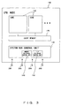
- Fig. 3 is a block diagram exemplifying the internal configuration of a CPU node 100 according to the present embodiment.
- the CPU node 100 comprises one processor core 110 or a plurality thereof, cache memory 120, and a system bus unit 130.
- the processor core 110 comprises an arithmetic logical operation function, such as an arithmetic logical operation unit (ALU), and a control function.
- ALU arithmetic logical operation unit
- the cache memory 120 temporarily stores information exchanged between the processor core 110 and the outside.
- the system bus control unit 130 controls the exchange of information between a plurality of system buses 200 connected to the CPU node 100.
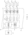
- the present embodiment is configured such that the system bus control unit 130 is equipped with a memory reference control unit 140 and an I/O reference control unit 150.
- the memory reference control unit 140 controls the memory interleave for a plurality of memory media 400 existing under the control of the individual system controllers of a plurality of system controllers 300 (i.e., system buses 200).
- the present embodiment is configured to control interleaving the memory at the level of the CPU node 100.
- the memory reference control unit 140 comprises an interleave control unit 141, a WAY mode setup register 142, and a memory access queue 143.
- the memory access queues 143 are equipped corresponding to respective packet generators 131, to which the system buses 200 (i.e., system controllers 300) are respectively connected.
- the interleave control unit 141 carries out a memory interleave by distributing access requests to the memory access queues 143 corresponding to the respective system buses 200 by way of the physical addresses (PA) (i.e., the lower 2 bits of SCREQ_BUSn in this case; in terms of the entirety of the system bus 200, 2 bits of PA [9:8] of the eighth and ninth from the lower bit) of reference target memory.
- PA physical addresses
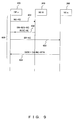
- the relationship between the physical address of a memory medium 400 and the corresponding system controller 300 is defined in the WAY mode setup register 142.
- WAY mode setup register 142 is how to distribute to any of the SCREQ_BUSn, in accordance with the 2 bits of the physical address PA [9:8], for each of the cases in which there are four system controllers 300 (SC) (per the configuration of Fig. 1 ) and in which there are two system controllers 300 (SC) (per the configuration of Fig. 1 minus the two options SC2 and SC3), as exemplified in Fig. 5 .
- the interleave control unit 141 refers to the WAY mode setup register 142 and distributes the memory access requests to the respective system controller 300 (i.e. , SC0 through SC3, or SC0 and SC1).
- the present embodiment is configured such that the I/O reference control unit 150 first inquires as to the whereabouts of the target I/O device 500 (i.e., the system bus 200 (i.e., system controller 300) where the I/O device 500 exists) from a representative system controller 300 (i.e., SC0 in this case) and then issues an actual I/O request to the system bus 200 (i.e., system controller 300) returned in the response from the SC0 and thereby the I/O access to the target I/O device 500 is carried out.
- a representative system controller 300 i.e., SC0 in this case
- the I/O reference control unit 150 is equipped with an I/O request queue 151 as exemplified in Fig. 6 .
- the I/O request queue 151 stores, starting from the processor core 110 side, I/O request frames 152 in order of occurrence of the I/O requests.
- An I/O request frame 152 is put together as a packet at the packet generator 131 and is sent to the system controller 300 by way of the system bus 200.
- the I/O request frame 152 includes a valid flag 152a, an I/O address 152b, an instruction code 152c, a byte mask 152d, a state variable 152e, an I/O request destination SC number 152f, and I/O data 152g.
- the valid flag 152a is information for controlling whether or not an I/O request frame 152 written in the I/O request queue 151 is to be enabled for execution.
- the I/O address 152b is the address of a target I/O device 500.
- the instruction code 152c sets an instruction to the I/O device 500.
- the byte mask 152d is information indicating which of the 24 bits (3 bytes) of SCREQ_BUSn the I/O data 152g is to be assigned to.
- the state variable 152e is information for managing the progress of I/O accesses executed in two separate events, as described above.
- the SC numbers (0 through 3) indicating the whereabouts of I/O device 500 that was returned in the response in response to the initial inquiry to the SC0 is set in the I/O request destination SC number 152f.
- Fig. 7 is a conceptual diagram exemplifying an I/O access transaction 600 executed by the I/O reference control unit 150.
- the I/O access transaction 600 is constituted by the first SC request 601 and first response SC order 602, and by the second SC request 603 and second response SC order 604.
- the first SC request 601 indicates an inquiry from the CPU node 100 to a specific SC0 regarding the whereabouts of an I/O device 500.
- transaction names 600a are defined as:
- the NC-RD is a request to the target I/O device 500 for reading I/O data 152g in units of bytes (e.g., 1 through 16 bytes).
- the NC-BD is a request to the target I/O device 500 for reading I/O data 152g in units of blocks (e.g., 64 bytes).
- the NC-WR is a request to the target I/O device 500 for writing I/O data 152g in units of bytes (e.g., 1 through 16 bytes).
- the NC-BW is a request to the target I/O device 500 for writing I/O data 152g in units of blocks (e.g., 64 bytes).
- the first response SC order 602 is the response from the SC0 to the first SC request 601.
- An I/O request destination SC number 152f is returned in this event.
- the issuance origin 600b is the SC0 and the issued destination 600c is the CPU (i.e., the CPU node 100).
- the SN-RES-NC responds with the number of the system controller 300 in which the inquired I/O device 500 exists.
- the SN-RES-AX is returned as a response if there is no I/O device 500 applicable to the designated address per the inquiry.
- the second SC request 603 is an execution of an I/O request to a target I/O device 500 existing under the control of a discretionary system controller 300 (SCn) identified by the I/O request destination SC number 152f.
- SCn discretionary system controller 300
- the SR-NC is a request to the I/O device 500 for reading in units of bytes.
- the SR-NB is a request to the I/O device 500 for reading in units blocks.
- the SW-NC is a request to the I/O device 500 for writing in units of bytes.
- the SW-NB is a request to the I/O device 500 for writing in units blocks.
- the issuance origin is the CPU node 100.
- the issued destination 600c is the SC number (SC-WAY) returned as a response from the SC0 by means of the first response SC order 602. That is, the fact that "BUS [1:0] designated" is defined in the issued destination 600c indicates that an I/O request must be issued to the SC-WAY designated by the SN-RES-NC.
- the second response SC order 604 is the response from the I/O device 500 (SCn) corresponding to the actual I/O request.
- the response to the write type is for responding as to whether or not a data write to the I/O device 500 is completed and is existent for controlling the releasing of a write-type I/O request.
- the issuance origin 600b in the second response SC order 604 is the same as the issued destination of the above described second SC request 603.
- the fact that "the same as SR-NC" is defined indicates that the second response SC order 604 (DOW) returns from the same place as the SCn that has issued the SR-NC.
- Fig. 8 is a state transition diagram exemplifying state transitions when executing the above described I/O transaction 600 at the I/O reference control unit 150.
- NC-RD as one example of the I/O transaction 600.
- the valid flag 152a is enabled and thereby the state is shifted to the first execution state 150b.
- the first SC request 601 (NC-RD) is issued to the SC0 (i.e., the first SC request 601), and the state is shifted to the first response wait state 150c, waiting for a response (SN-RES-NC or SN-RES-AX) from the SC0.
- the I/O reference control unit 150 Having received the SN-RES-NC or SN-RES-AX from the SC0 (i.e., the first response SC order 602), the I/O reference control unit 150 shifts the state to the second execution state 150d.
- the I/O reference control unit 150 issues an SR-NC (i.e., the second SC request 603) to a system bus 200 corresponding to the designated SCn and shifts the state to the second response wait state 150e.
- SR-NC i.e., the second SC request 603
- the I/O reference control unit 150 receives response information (i.e., the second response SC order 604) from the target I/O device 500 by way of the SCn and returns the state to the initial state 150a.
- response information i.e., the second response SC order 604
- the I/O reference control unit 150 carries out a prescribed error process, because the target I/O device 500 designated by the I/O address 152b does not exist, and returns to the initial state 150a.
- Fig. 9 is a sequence diagram exemplifying the execution of a transaction related to an NC-RD as one example of an I/O access transaction 600.
- the CPU node 100 issues an NC-RD to a specific SC0 (i.e., a system bus 200: SCREQ_BUS0) and inquires into an SC number where the I/O device 500 of a target I/O address (which is the first SC request 601).
- a specific SC0 i.e., a system bus 200: SCREQ_BUS0
- SCREQ_BUS0 system bus 200
- the SC0 responds to the CPU node 100, which is the issuance origin, with the SC number of the system controller 300 having the target I/O device 500 under the control thereof by means of the SN-RES-NC (which is the first response SC order 602).
- the CPU node 100 issues an I/O request for the I/O device 500, via SR-NC, to the system controller 300 (i.e., the system bus 200) of the SC number received by means of the first response SC order 602 (which is second SC request 603).
- the system controller 300 i.e., the system bus 200
- the present embodiment is configured such that the memory reference control unit 140 comprised by the CPU node 100 distributes, to a plurality of the memory media 400 (i.e., the system controllers 300) in accordance with physical addresses, the memory references into the memory media 400 and thereby an interleave is carried out in units of, for example, 256 bytes.
- This configuration makes it possible to reduce the number of signal lines of the buses between the CPU node 100 and system controller 300 in comparison with the case of carrying out a centralized interleaving at a single system controller 300.
- the configuration makes it possible to exert the processing capability of the CPU node 100 sufficiently by speeding up the accesses thereof to the memory media 400 without increasing the production costs of the system controller 300. and the information processing system comprising the present system controller 300.
- an inquiry to a representative system controller 300 makes it possible to execute an I/O request by way of certain steps, that is, the process of knowing the position of the target I/O device 500 and the process of executing an actual I/O request to the obtained I/O device 500 (i.e., the system controller 300, i.e., the system bus 200).
- This configuration makes it possible to achieve an appropriate I/O access to a plurality of I/O devices 500 in which the I/O addresses are mapped in the memory address space even when executing a memory interleave at the CPU node 100.
- the configuration makes it possible to achieve, in the individual CPU nodes 100, an appropriate I/O access to a plurality of I/O devices 500 in which the I/O addresses are mapped in the memory address space without requiring a storage resource for storing the affiliation information of a plurality of I/O devices 500 against a system controller(s) 300, or similar information, and without requiring a complicated control such as managing the aforementioned affiliation information.
- FIG. 10 shows an example implementation of the CPU nodes 100 and system controllers 300 that are exemplified in Fig. 1 .
- the CPU nodes 100 and system controllers 300 which constitute the information processing system, comprise one or more system boards 10.
- the system controller 300 behaves as a single logical system controller 300 (SCn) as a result of connecting a plurality of semiconductor chips 301 by way of a crossbar switch 11 or the like.
- the SC0 enclosed by the dotted line box in Fig. 10 is equivalent to the SC0 (i.e., the system controller 300) exemplified in Fig. 1 .
- the present invention makes it possible to attain a high memory bandwidth and to utilize the processing capability of a central processing apparatus effectively without complicating the configuration of system controllers connected to the central processing apparatus.
- the present invention makes it possible to achieve an improvement in the processing capability of a central processing apparatus executing a memory interleave at a low cost without complicating the configuration or management of the central processing apparatus.
Landscapes
- Engineering & Computer Science (AREA)
- Theoretical Computer Science (AREA)
- Physics & Mathematics (AREA)
- General Engineering & Computer Science (AREA)
- General Physics & Mathematics (AREA)
- Bus Control (AREA)
- Multi Processors (AREA)
Claims (6)
- Zentralprozessorvorrichtung (100), umfassend:eine Bussteuereinheit (130) zum Durchführen von Eingabe/Ausgabe von Information zwischen einer Mehrzahl von Bussen (200), die mit einer Systemsteuerung (300) verbunden sind; undeine Speicherzugriffssteuereinheit (140) zum Verteilen von Speicherzugriffsanfragen an eine Mehrzahl der Busse (200) in Übereinstimmung mit Speicheradressen, und dadurch gekennzeichnet, dass sie umfasst:eine Eingabe/Ausgabe-Zugriffssteuereinheit (150) zum Zugreifen auf eine externe Eingabe/Ausgabevorrichtung (500) vermittels eines Busses, wobei die Eingabe/Ausgabe-Zugriffssteuereinheit (150) konfiguriert ist, auszuführeneinen ersten Schritt des Anfragens, bei der Systemsteuerung (300), durch einen spezifischen der Mehrzahl von Bussen (200), auf welchem der Mehrzahl von Bussen (200) die Eingabe/Ausgabevorrichtung (500) eines Zugriffziels existiert, undeinen zweiten Schritt des Zugreifens auf die Eingabe/Ausgabevorrichtung (500) unter Verwendung des Busses (200), der in einer Antwort aus der Systemsteuerung (300) rückgegeben wird.
- Zentralprozessorvorrichtung (100) gemäß Anspruch 1, wobei
die Speicherzugriffssteuereinheit (140) konfiguriert ist, eine Speicherverwebung für paralleles Zugreifen, in Übereinstimmung mit den Speicheradressen, auf eine Mehrzahl von Speichermedien (400) durchzuführen, die individuell mit einer Mehrzahl der Busse (200) verbunden sind. - Steuerverfahren, das für eine
Zentralprozessorvorrichtung (100) verwendet wird, umfassend die Schritte:Verbinden der Zentralprozessorvorrichtung (100) mit einer Mehrzahl von Bussen (200), die mit einer Systemsteuerung (300) verbunden sind; undwobei die Zentralprozessorvorrichtung (100) eine Speicherverwebung zum Verteilen einer Mehrzahl von Speicherzugriffsanfragen an Speichermedien (400), die auf den Bussen (200) existieren, in Übereinstimmung mit Speicheradressen durchführt,weiter umfassend die Schritte:Anfragen, der Zentralprozessorvorrichtung (100), bei der Systemsteuerung (300) mittels eines spezifischen der Mehrzahl von Bussen (200), auf welchem der Mehrzahl von Bussen (200) eine Eingabe/Ausgabevorrichtung (500) eines Zugriffziels existiert, undZugreifen, der Zentralprozessorvorrichtung (100), auf die Eingabe/Ausgabevorrichtung (500) unter Verwendung des Busses (200), auf den aus einer Systemsteuerung geantwortet wird. - Informationsverarbeitungssystem, umfassend:die Zentralprozessorvorrichtung (100) gemäß Anspruch 1;eine Mehrzahl von Systemsteuerungen (300), einschließlich der Systemsteuerung (300), von denen jede mit entweder einem Speichermedium (400) oder einer Eingabe/Ausgabevorrichtung (500) verbunden ist, unter der Steuerung jeder der Mehrzahl von Systemsteuerungen (300); undwobei die Mehrzahl von Bussen (200) jeweils zwischen der Zentralprozessorvorrichtung (100) und einzelnen Systemsteuerungen (300) verbindet;wobei die Speicherzugriffssteuereinheit (140) konfiguriert ist, die Speicherzugriffsanfragen an Speichermedien (400), die auf der Mehrzahl von Bussen (200) existieren, in Übereinstimmung mit den Speicheradressen zu verteilen.
- Informationsverarbeitungssystem gemäß Anspruch 4, wobei
jede einer Mehrzahl von Zentralprozessorvorrichtungen (100) mit einer individuellen Systemsteuerung (300) einer Mehrzahl der Systemsteuerungen (300) jeweils verbunden ist, mittels einer Mehrzahl der Busse (200). - Informationsprozesssystem gemäß Anspruch 4, wobei
jede der Systemsteuerungen (300) aus einer Mehrzahl von Halbleiterchips aufgebaut ist.
Applications Claiming Priority (1)
| Application Number | Priority Date | Filing Date | Title |
|---|---|---|---|
| PCT/JP2006/303649 WO2007097036A1 (ja) | 2006-02-27 | 2006-02-27 | 中央処理装置、中央処理装置の制御方法、情報処理システム |
Publications (3)
| Publication Number | Publication Date |
|---|---|
| EP1990725A1 EP1990725A1 (de) | 2008-11-12 |
| EP1990725A4 EP1990725A4 (de) | 2010-08-25 |
| EP1990725B1 true EP1990725B1 (de) | 2016-08-10 |
Family
ID=38437095
Family Applications (1)
| Application Number | Title | Priority Date | Filing Date |
|---|---|---|---|
| EP06714786.8A Expired - Fee Related EP1990725B1 (de) | 2006-02-27 | 2006-02-27 | Zentrale verarbeitungseinheit, steuerverfahren für eine zentrale verarbeitungseinheit und informationsverarbeitungssystem |
Country Status (4)
| Country | Link |
|---|---|
| US (1) | US8015326B2 (de) |
| EP (1) | EP1990725B1 (de) |
| JP (1) | JP4774099B2 (de) |
| WO (1) | WO2007097036A1 (de) |
Families Citing this family (1)
| Publication number | Priority date | Publication date | Assignee | Title |
|---|---|---|---|---|
| DE102018205204A1 (de) | 2018-04-06 | 2019-10-10 | Robert Bosch Gmbh | Verfahren zum Bereitstellen von Anwendungsdaten zumindest einer auf einem Steuergerät eines Fahrzeugs ausführbaren Anwendung, Verfahren zum Kalibrieren eines Steuergeräts, Steuergerät und Auswerteeinrichtung |
Family Cites Families (23)
| Publication number | Priority date | Publication date | Assignee | Title |
|---|---|---|---|---|
| US3307984A (en) * | 1962-12-07 | 1967-03-07 | Trw Semiconductors Inc | Method of forming diode with high resistance substrate |
| US4207609A (en) * | 1978-05-08 | 1980-06-10 | International Business Machines Corporation | Method and means for path independent device reservation and reconnection in a multi-CPU and shared device access system |
| AU541189B2 (en) * | 1980-02-11 | 1984-12-20 | Data General Corporation | Data processing system |
| US4435755A (en) * | 1981-12-28 | 1984-03-06 | International Business Machines Corporation | Balanced channel finding method |
| US4697232A (en) * | 1984-11-30 | 1987-09-29 | Storage Technology Corporation | I/O device reconnection in a multiple-CPU, dynamic path allocation environment |
| JP3134364B2 (ja) * | 1991-07-17 | 2001-02-13 | 日本電気株式会社 | 情報処理システム |
| JPH05252228A (ja) * | 1992-03-02 | 1993-09-28 | Mitsubishi Electric Corp | データ伝送装置及びその通信路管理方法 |
| DE69324399T2 (de) * | 1992-04-29 | 1999-09-30 | Canon Kk | Videoprozessorsystem |
| US5542055A (en) * | 1993-05-28 | 1996-07-30 | International Business Machines Corp. | System for counting the number of peripheral buses in each hierarch connected to primary bus for creating map of peripheral buses to locate peripheral devices |
| JPH0764848A (ja) * | 1993-08-23 | 1995-03-10 | Hitachi Ltd | 計算機システムおよび計算機システムの構成変更方法 |
| WO1995022106A1 (en) * | 1994-02-10 | 1995-08-17 | Elonex Technologies, Inc. | I/o decoder map |
| JPH10254820A (ja) * | 1997-03-06 | 1998-09-25 | Canon Inc | バス制御装置およびバス制御装置のバス制御方法およびコンピュータが読み出し可能なプログラムを格納した記憶媒体 |
| US5958024A (en) * | 1997-08-29 | 1999-09-28 | Advanced Micro Devices, Inc. | System having a receive data register for storing at least nine data bits of frame and status bits indicating the status of asynchronous serial receiver |
| US6145028A (en) * | 1997-12-11 | 2000-11-07 | Ncr Corporation | Enhanced multi-pathing to an array of storage devices |
| US6356991B1 (en) * | 1997-12-31 | 2002-03-12 | Unisys Corporation | Programmable address translation system |
| US6185654B1 (en) * | 1998-07-17 | 2001-02-06 | Compaq Computer Corporation | Phantom resource memory address mapping system |
| US6850997B1 (en) * | 2000-09-27 | 2005-02-01 | International Business Machines Corporation | System, method, and program for determining the availability of paths to a device |
| US6957219B1 (en) * | 2001-11-15 | 2005-10-18 | Microsoft Corporation | System and method of pipeline data access to remote data |
| US7406039B2 (en) * | 2002-02-26 | 2008-07-29 | Dell Products L.P. | System and method for a failover protocol in storage area network controllers |
| JP3848587B2 (ja) * | 2002-03-15 | 2006-11-22 | 株式会社日立製作所 | 情報処理装置および通信路選択方法 |
| US20050138276A1 (en) * | 2003-12-17 | 2005-06-23 | Intel Corporation | Methods and apparatus for high bandwidth random access using dynamic random access memory |
| JP2005301880A (ja) * | 2004-04-15 | 2005-10-27 | Hitachi Ltd | 計算機システムにおけるデータ入出力処理方法、ストレージ装置、ホスト計算機、および計算機システム、 |
| JP4963808B2 (ja) * | 2005-08-05 | 2012-06-27 | 株式会社日立製作所 | 記憶制御システム |
-
2006
- 2006-02-27 WO PCT/JP2006/303649 patent/WO2007097036A1/ja active Application Filing
- 2006-02-27 JP JP2008501586A patent/JP4774099B2/ja not_active Expired - Fee Related
- 2006-02-27 EP EP06714786.8A patent/EP1990725B1/de not_active Expired - Fee Related
-
2008
- 2008-08-27 US US12/199,004 patent/US8015326B2/en not_active Expired - Fee Related
Also Published As
| Publication number | Publication date |
|---|---|
| JP4774099B2 (ja) | 2011-09-14 |
| WO2007097036A1 (ja) | 2007-08-30 |
| EP1990725A4 (de) | 2010-08-25 |
| US20080320201A1 (en) | 2008-12-25 |
| EP1990725A1 (de) | 2008-11-12 |
| US8015326B2 (en) | 2011-09-06 |
| JPWO2007097036A1 (ja) | 2009-07-09 |
Similar Documents
| Publication | Publication Date | Title |
|---|---|---|
| US11907528B2 (en) | Multi-processor bridge with cache allocate awareness | |
| JP3807250B2 (ja) | クラスタシステム、コンピュータ及びプログラム | |
| US20050038941A1 (en) | Method and apparatus for accessing a memory | |
| JP2002510079A (ja) | メモリ・インタフェース間で読み書きの順序付けられた実行を強制する方法と装置 | |
| KR20020009823A (ko) | 버스 시스템 및 그 버스 중재방법 | |
| CN114003168B (zh) | 用于处理命令的存储设备和方法 | |
| US6701387B1 (en) | Adaptive data fetch prediction algorithm | |
| US6128689A (en) | System for exchanging data through data memory area of common memory in synchronous and asynchronous modes | |
| EP1990725B1 (de) | Zentrale verarbeitungseinheit, steuerverfahren für eine zentrale verarbeitungseinheit und informationsverarbeitungssystem | |
| US6847990B2 (en) | Data transfer unit with support for multiple coherency granules | |
| CN115328832B (zh) | 一种基于pcie dma的数据调度系统与方法 | |
| US20240184446A1 (en) | Multi-processor bridge with cache allocate awareness | |
| JP2001273191A (ja) | コンピュータシステム | |
| WO2011030498A1 (ja) | データ処理装置及びデータ処理方法 | |
| KR19990071122A (ko) | 다중 프로세서 회로 | |
| JP4496923B2 (ja) | 共有メモリシステム | |
| JP4521410B2 (ja) | ディスクアレイ制御装置 | |
| WO2003048955A1 (fr) | Systeme multiprocesseur | |
| JPS63259746A (ja) | バンクメモリ間のデ−タ転送方式 | |
| JPH0690711B2 (ja) | メモリアクセス制御方式 | |
| JP2003085040A (ja) | メモリアクセラレータ、アクセラレーション方法、および、これに関連したインターフェースカードおよびマザーボード | |
| JPH09223120A (ja) | マルチプロセッサシステム | |
| JPS62226366A (ja) | メモリ共有方式 | |
| JPH06131246A (ja) | 共有メモリの非同期アクセス方式 | |
| JPH10269191A (ja) | メッセージ受信方式 |
Legal Events
| Date | Code | Title | Description |
|---|---|---|---|
| PUAI | Public reference made under article 153(3) epc to a published international application that has entered the european phase |
Free format text: ORIGINAL CODE: 0009012 |
|
| 17P | Request for examination filed |
Effective date: 20080924 |
|
| AK | Designated contracting states |
Kind code of ref document: A1 Designated state(s): DE FR GB |
|
| DAX | Request for extension of the european patent (deleted) | ||
| RBV | Designated contracting states (corrected) |
Designated state(s): DE FR GB |
|
| A4 | Supplementary search report drawn up and despatched |
Effective date: 20100726 |
|
| 17Q | First examination report despatched |
Effective date: 20141024 |
|
| GRAP | Despatch of communication of intention to grant a patent |
Free format text: ORIGINAL CODE: EPIDOSNIGR1 |
|
| INTG | Intention to grant announced |
Effective date: 20160301 |
|
| RAP1 | Party data changed (applicant data changed or rights of an application transferred) |
Owner name: FUJITSU LIMITED |
|
| RIN1 | Information on inventor provided before grant (corrected) |
Inventor name: UKAI, MASAKI Inventor name: UNNO, HIDEYUKI |
|
| GRAS | Grant fee paid |
Free format text: ORIGINAL CODE: EPIDOSNIGR3 |
|
| GRAA | (expected) grant |
Free format text: ORIGINAL CODE: 0009210 |
|
| AK | Designated contracting states |
Kind code of ref document: B1 Designated state(s): DE FR GB |
|
| REG | Reference to a national code |
Ref country code: GB Ref legal event code: FG4D |
|
| REG | Reference to a national code |
Ref country code: DE Ref legal event code: R096 Ref document number: 602006049861 Country of ref document: DE |
|
| REG | Reference to a national code |
Ref country code: FR Ref legal event code: PLFP Year of fee payment: 12 |
|
| REG | Reference to a national code |
Ref country code: DE Ref legal event code: R097 Ref document number: 602006049861 Country of ref document: DE |
|
| PLBE | No opposition filed within time limit |
Free format text: ORIGINAL CODE: 0009261 |
|
| STAA | Information on the status of an ep patent application or granted ep patent |
Free format text: STATUS: NO OPPOSITION FILED WITHIN TIME LIMIT |
|
| 26N | No opposition filed |
Effective date: 20170511 |
|
| REG | Reference to a national code |
Ref country code: FR Ref legal event code: PLFP Year of fee payment: 13 |
|
| PGFP | Annual fee paid to national office [announced via postgrant information from national office to epo] |
Ref country code: FR Payment date: 20210113 Year of fee payment: 16 |
|
| PGFP | Annual fee paid to national office [announced via postgrant information from national office to epo] |
Ref country code: GB Payment date: 20210217 Year of fee payment: 16 Ref country code: DE Payment date: 20210216 Year of fee payment: 16 |
|
| REG | Reference to a national code |
Ref country code: DE Ref legal event code: R119 Ref document number: 602006049861 Country of ref document: DE |
|
| GBPC | Gb: european patent ceased through non-payment of renewal fee |
Effective date: 20220227 |
|
| PG25 | Lapsed in a contracting state [announced via postgrant information from national office to epo] |
Ref country code: FR Free format text: LAPSE BECAUSE OF NON-PAYMENT OF DUE FEES Effective date: 20220228 |
|
| PG25 | Lapsed in a contracting state [announced via postgrant information from national office to epo] |
Ref country code: GB Free format text: LAPSE BECAUSE OF NON-PAYMENT OF DUE FEES Effective date: 20220227 Ref country code: DE Free format text: LAPSE BECAUSE OF NON-PAYMENT OF DUE FEES Effective date: 20220901 |