EP1981069A2 - Verfahren zur Herstellung eines Gruppe-III-V-Verbindungshalbleiters, Schottky-Barrierendiode, Lichtemissionsdiode, Laserdiode und Herstellungsverfahren für die Dioden - Google Patents
Verfahren zur Herstellung eines Gruppe-III-V-Verbindungshalbleiters, Schottky-Barrierendiode, Lichtemissionsdiode, Laserdiode und Herstellungsverfahren für die Dioden Download PDFInfo
- Publication number
- EP1981069A2 EP1981069A2 EP08003392A EP08003392A EP1981069A2 EP 1981069 A2 EP1981069 A2 EP 1981069A2 EP 08003392 A EP08003392 A EP 08003392A EP 08003392 A EP08003392 A EP 08003392A EP 1981069 A2 EP1981069 A2 EP 1981069A2
- Authority
- EP
- European Patent Office
- Prior art keywords
- group iii
- type
- compound semiconductor
- ppm
- producing
- Prior art date
- Legal status (The legal status is an assumption and is not a legal conclusion. Google has not performed a legal analysis and makes no representation as to the accuracy of the status listed.)
- Withdrawn
Links
Images


Classifications
-
- H10P14/3442—
-
- B—PERFORMING OPERATIONS; TRANSPORTING
- B82—NANOTECHNOLOGY
- B82Y—SPECIFIC USES OR APPLICATIONS OF NANOSTRUCTURES; MEASUREMENT OR ANALYSIS OF NANOSTRUCTURES; MANUFACTURE OR TREATMENT OF NANOSTRUCTURES
- B82Y20/00—Nanooptics, e.g. quantum optics or photonic crystals
-
- C—CHEMISTRY; METALLURGY
- C23—COATING METALLIC MATERIAL; COATING MATERIAL WITH METALLIC MATERIAL; CHEMICAL SURFACE TREATMENT; DIFFUSION TREATMENT OF METALLIC MATERIAL; COATING BY VACUUM EVAPORATION, BY SPUTTERING, BY ION IMPLANTATION OR BY CHEMICAL VAPOUR DEPOSITION, IN GENERAL; INHIBITING CORROSION OF METALLIC MATERIAL OR INCRUSTATION IN GENERAL
- C23C—COATING METALLIC MATERIAL; COATING MATERIAL WITH METALLIC MATERIAL; SURFACE TREATMENT OF METALLIC MATERIAL BY DIFFUSION INTO THE SURFACE, BY CHEMICAL CONVERSION OR SUBSTITUTION; COATING BY VACUUM EVAPORATION, BY SPUTTERING, BY ION IMPLANTATION OR BY CHEMICAL VAPOUR DEPOSITION, IN GENERAL
- C23C16/00—Chemical coating by decomposition of gaseous compounds, without leaving reaction products of surface material in the coating, i.e. chemical vapour deposition [CVD] processes
- C23C16/22—Chemical coating by decomposition of gaseous compounds, without leaving reaction products of surface material in the coating, i.e. chemical vapour deposition [CVD] processes characterised by the deposition of inorganic material, other than metallic material
- C23C16/30—Deposition of compounds, mixtures or solid solutions, e.g. borides, carbides, nitrides
- C23C16/301—AIII BV compounds, where A is Al, Ga, In or Tl and B is N, P, As, Sb or Bi
- C23C16/303—Nitrides
-
- H—ELECTRICITY
- H10—SEMICONDUCTOR DEVICES; ELECTRIC SOLID-STATE DEVICES NOT OTHERWISE PROVIDED FOR
- H10D—INORGANIC ELECTRIC SEMICONDUCTOR DEVICES
- H10D30/00—Field-effect transistors [FET]
- H10D30/01—Manufacture or treatment
- H10D30/015—Manufacture or treatment of FETs having heterojunction interface channels or heterojunction gate electrodes, e.g. HEMT
-
- H—ELECTRICITY
- H10—SEMICONDUCTOR DEVICES; ELECTRIC SOLID-STATE DEVICES NOT OTHERWISE PROVIDED FOR
- H10D—INORGANIC ELECTRIC SEMICONDUCTOR DEVICES
- H10D30/00—Field-effect transistors [FET]
- H10D30/40—FETs having zero-dimensional [0D], one-dimensional [1D] or two-dimensional [2D] charge carrier gas channels
- H10D30/47—FETs having zero-dimensional [0D], one-dimensional [1D] or two-dimensional [2D] charge carrier gas channels having 2D charge carrier gas channels, e.g. nanoribbon FETs or high electron mobility transistors [HEMT]
- H10D30/471—High electron mobility transistors [HEMT] or high hole mobility transistors [HHMT]
- H10D30/475—High electron mobility transistors [HEMT] or high hole mobility transistors [HHMT] having wider bandgap layer formed on top of lower bandgap active layer, e.g. undoped barrier HEMTs such as i-AlGaN/GaN HEMTs
-
- H—ELECTRICITY
- H10—SEMICONDUCTOR DEVICES; ELECTRIC SOLID-STATE DEVICES NOT OTHERWISE PROVIDED FOR
- H10D—INORGANIC ELECTRIC SEMICONDUCTOR DEVICES
- H10D8/00—Diodes
- H10D8/01—Manufacture or treatment
- H10D8/051—Manufacture or treatment of Schottky diodes
-
- H—ELECTRICITY
- H10—SEMICONDUCTOR DEVICES; ELECTRIC SOLID-STATE DEVICES NOT OTHERWISE PROVIDED FOR
- H10D—INORGANIC ELECTRIC SEMICONDUCTOR DEVICES
- H10D8/00—Diodes
- H10D8/60—Schottky-barrier diodes
-
- H—ELECTRICITY
- H10—SEMICONDUCTOR DEVICES; ELECTRIC SOLID-STATE DEVICES NOT OTHERWISE PROVIDED FOR
- H10H—INORGANIC LIGHT-EMITTING SEMICONDUCTOR DEVICES HAVING POTENTIAL BARRIERS
- H10H20/00—Individual inorganic light-emitting semiconductor devices having potential barriers, e.g. light-emitting diodes [LED]
- H10H20/01—Manufacture or treatment
- H10H20/011—Manufacture or treatment of bodies, e.g. forming semiconductor layers
- H10H20/013—Manufacture or treatment of bodies, e.g. forming semiconductor layers having light-emitting regions comprising only Group III-V materials
- H10H20/0137—Manufacture or treatment of bodies, e.g. forming semiconductor layers having light-emitting regions comprising only Group III-V materials the light-emitting regions comprising nitride materials
-
- H—ELECTRICITY
- H10—SEMICONDUCTOR DEVICES; ELECTRIC SOLID-STATE DEVICES NOT OTHERWISE PROVIDED FOR
- H10H—INORGANIC LIGHT-EMITTING SEMICONDUCTOR DEVICES HAVING POTENTIAL BARRIERS
- H10H20/00—Individual inorganic light-emitting semiconductor devices having potential barriers, e.g. light-emitting diodes [LED]
- H10H20/80—Constructional details
- H10H20/81—Bodies
- H10H20/822—Materials of the light-emitting regions
- H10H20/824—Materials of the light-emitting regions comprising only Group III-V materials, e.g. GaP
- H10H20/825—Materials of the light-emitting regions comprising only Group III-V materials, e.g. GaP containing nitrogen, e.g. GaN
- H10H20/8252—Materials of the light-emitting regions comprising only Group III-V materials, e.g. GaP containing nitrogen, e.g. GaN characterised by the dopants
-
- H10P14/24—
-
- H10P14/2908—
-
- H10P14/3216—
-
- H10P14/3251—
-
- H10P14/3416—
-
- H10P14/3438—
-
- H—ELECTRICITY
- H01—ELECTRIC ELEMENTS
- H01S—DEVICES USING THE PROCESS OF LIGHT AMPLIFICATION BY STIMULATED EMISSION OF RADIATION [LASER] TO AMPLIFY OR GENERATE LIGHT; DEVICES USING STIMULATED EMISSION OF ELECTROMAGNETIC RADIATION IN WAVE RANGES OTHER THAN OPTICAL
- H01S2304/00—Special growth methods for semiconductor lasers
- H01S2304/04—MOCVD or MOVPE
-
- H—ELECTRICITY
- H01—ELECTRIC ELEMENTS
- H01S—DEVICES USING THE PROCESS OF LIGHT AMPLIFICATION BY STIMULATED EMISSION OF RADIATION [LASER] TO AMPLIFY OR GENERATE LIGHT; DEVICES USING STIMULATED EMISSION OF ELECTROMAGNETIC RADIATION IN WAVE RANGES OTHER THAN OPTICAL
- H01S5/00—Semiconductor lasers
- H01S5/20—Structure or shape of the semiconductor body to guide the optical wave ; Confining structures perpendicular to the optical axis, e.g. index or gain guiding, stripe geometry, broad area lasers, gain tailoring, transverse or lateral reflectors, special cladding structures, MQW barrier reflection layers
- H01S5/2004—Confining in the direction perpendicular to the layer structure
- H01S5/2009—Confining in the direction perpendicular to the layer structure by using electron barrier layers
-
- H—ELECTRICITY
- H01—ELECTRIC ELEMENTS
- H01S—DEVICES USING THE PROCESS OF LIGHT AMPLIFICATION BY STIMULATED EMISSION OF RADIATION [LASER] TO AMPLIFY OR GENERATE LIGHT; DEVICES USING STIMULATED EMISSION OF ELECTROMAGNETIC RADIATION IN WAVE RANGES OTHER THAN OPTICAL
- H01S5/00—Semiconductor lasers
- H01S5/30—Structure or shape of the active region; Materials used for the active region
- H01S5/305—Structure or shape of the active region; Materials used for the active region characterised by the doping materials used in the laser structure
- H01S5/3054—Structure or shape of the active region; Materials used for the active region characterised by the doping materials used in the laser structure p-doping
-
- H—ELECTRICITY
- H01—ELECTRIC ELEMENTS
- H01S—DEVICES USING THE PROCESS OF LIGHT AMPLIFICATION BY STIMULATED EMISSION OF RADIATION [LASER] TO AMPLIFY OR GENERATE LIGHT; DEVICES USING STIMULATED EMISSION OF ELECTROMAGNETIC RADIATION IN WAVE RANGES OTHER THAN OPTICAL
- H01S5/00—Semiconductor lasers
- H01S5/30—Structure or shape of the active region; Materials used for the active region
- H01S5/32—Structure or shape of the active region; Materials used for the active region comprising PN junctions, e.g. hetero- or double- heterostructures
- H01S5/3211—Structure or shape of the active region; Materials used for the active region comprising PN junctions, e.g. hetero- or double- heterostructures characterised by special cladding layers, e.g. details on band-discontinuities
-
- H—ELECTRICITY
- H01—ELECTRIC ELEMENTS
- H01S—DEVICES USING THE PROCESS OF LIGHT AMPLIFICATION BY STIMULATED EMISSION OF RADIATION [LASER] TO AMPLIFY OR GENERATE LIGHT; DEVICES USING STIMULATED EMISSION OF ELECTROMAGNETIC RADIATION IN WAVE RANGES OTHER THAN OPTICAL
- H01S5/00—Semiconductor lasers
- H01S5/30—Structure or shape of the active region; Materials used for the active region
- H01S5/34—Structure or shape of the active region; Materials used for the active region comprising quantum well or superlattice structures, e.g. single quantum well [SQW] lasers, multiple quantum well [MQW] lasers or graded index separate confinement heterostructure [GRINSCH] lasers
- H01S5/343—Structure or shape of the active region; Materials used for the active region comprising quantum well or superlattice structures, e.g. single quantum well [SQW] lasers, multiple quantum well [MQW] lasers or graded index separate confinement heterostructure [GRINSCH] lasers in AIIIBV compounds, e.g. AlGaAs-laser, InP-based laser
- H01S5/34333—Structure or shape of the active region; Materials used for the active region comprising quantum well or superlattice structures, e.g. single quantum well [SQW] lasers, multiple quantum well [MQW] lasers or graded index separate confinement heterostructure [GRINSCH] lasers in AIIIBV compounds, e.g. AlGaAs-laser, InP-based laser with a well layer based on Ga(In)N or Ga(In)P, e.g. blue laser
-
- H—ELECTRICITY
- H10—SEMICONDUCTOR DEVICES; ELECTRIC SOLID-STATE DEVICES NOT OTHERWISE PROVIDED FOR
- H10D—INORGANIC ELECTRIC SEMICONDUCTOR DEVICES
- H10D62/00—Semiconductor bodies, or regions thereof, of devices having potential barriers
- H10D62/80—Semiconductor bodies, or regions thereof, of devices having potential barriers characterised by the materials
- H10D62/85—Semiconductor bodies, or regions thereof, of devices having potential barriers characterised by the materials being Group III-V materials, e.g. GaAs
- H10D62/8503—Nitride Group III-V materials, e.g. AlN or GaN
Definitions
- the present invention relates generally to methods of producing group III-V compound semiconductors, Schottky barrier diodes, light emitting diodes, laser diodes and methods of fabricating such diodes.
- the present invention relates to methods of producing group III-V compound semiconductors, Schottky barrier diodes, light emitting diodes, laser diodes and methods of fabricating such diodes, that can achieve a reduced n type carrier density.
- Group III-V compound semiconductor is significantly useful for Schottky barrier diodes, light emitting diodes (LEDs), laser diodes (LD) and other similar semiconductor devices.
- LEDs light emitting diodes
- LD laser diodes
- group III-V compound semiconductor for example sublimination, hydride vapor phase epitaxy (HVPE), molecular beam epitaxy (MBE), metal organic chemical vapor deposition (MOCVD) and the like vapor phase epitaxy have conventionally been proposed.
- HVPE hydride vapor phase epitaxy
- MBE molecular beam epitaxy
- MOCVD metal organic chemical vapor deposition
- MOCVD is one representative vapor phase epitaxy. It vaporizes an organic metal serving as a material containing a group III element and thermally decomposes the vaporized material at a surface of a substrate and causes the decomposed material to react with a gas containing a group V element to deposit a film.
- This method can control a film in thickness, composition and the like and is also excellently productive. The method is thus widely used as a technique for deposition in producing group III-V compound semiconductor.
- the material containing the group III element that is used in MOCVD can for example be an organometallic compound produced in a method of producing an organometallic compound as disclosed in Japanese Patent Laying-Open No. 2006-342101 .
- the publication discloses a method of producing an organometallic compound containing less than 0.05 ppm of organic silicon, less than 10 ppm of oxygen and less than 10 ppm of silicon carbide as impurities.
- the group III-V compound semiconductor has a disadvantageously high n type carrier density without n type impurity introduced. If such group III-V compound semiconductor is used to form a drift layer of a Schottky barrier diode, the drift layer has an excessively high n type carrier density and also cannot be controlled to have a carrier density lower than that high density. Furthermore, if an LED or the like is fabricated and a p type, group III-V compound semiconductor is to be grown, n type impurity concentration must be significantly reduced.
- the group III-V compound semiconductor has an excessively high n type carrier density, and methods of producing a group III-V compound semiconductor having a low n type carrier density, a p type group III-V compound semiconductor and the like have room for improvement.
- the present invention therefore contemplates a method of producing a group III-V compound semiconductor, a Schottky barrier diode, a light emitting diode, a laser diode, and a method of fabricating them, that can achieve a reduced n type carrier density.
- the present inventors have conducted a thorough study to find a condition allowing an undoped, group III-V compound semiconductor to be grown to have an n type carrier density reduced to a density (for example of at most 5 ⁇ 10 15 cm -3 ).
- the present invention provides a method of producing a group III-V compound semiconductor by metal organic chemical vapor deposition employing a material containing a group III element, including the steps of: initially preparing a seed substrate; and growing the group III-V compound semiconductor on the seed substrate by employing an organic metal as the material containing the group III element, the organic metal containing at most 0.01 ppm of silicon, at most 10 ppm of oxygen, and less than 0.04 ppm of germanium.
- an organic metal serving as a material containing a group III element can be used that contains impurities of silicon, oxygen and germanium having upper limits of at most 0.01 ppm, at most 10 ppm and less than 0.04 ppm, respectively.
- the group III-V compound semiconductor can have an n type carrier density reduced to a desired density (for example of at most 5 ⁇ 10 15 cm -3 ). Conventionally it has been difficult to control n type carrier density within a low density range.
- the present invention as described above, can help to control n type carrier density in such range, and also achieve a reduced n type impurity conventionally required in producing p type, group III-V compound semiconductor.
- the above silicon content is a value as measured by inductively coupled plasma-atomic emission spectroscopy (ICP-AES).
- the above oxygen content is a value as measured by Fourier Transform-nuclear magnetic resonance (FT-NMR).
- the above germanium content is a value as measured by inductively coupled plasma-mass spectroscopy (ICP-MS).
- the organic metal is at least one type of substance selected from the group consisting of trimethylgallium, triethylgallium, trimethylaluminum, and trimethylindium.
- the organic metal that is at least one of trimethylgallium, triethylgallium, trimethylaluminum, and trimethylindium is effective in producing an undoped, group III-V compound semiconductor.
- Al x Ga y In (1-x-y) N is grown as the group III-V compound semiconductor, wherein 0 ⁇ x ⁇ 1, 0 ⁇ y ⁇ 1, and x + y ⁇ 1.
- a group III-V compound semiconductor formed of Al x Ga y In (1-x-y) N having a reduced n type carrier density can be grown, wherein 0 ⁇ x ⁇ 1, 0 ⁇ y ⁇ 1, and x + y ⁇ 1.
- gallium nitride is grown as the group III-V compound semiconductor.
- group III-V compound semiconductor can be produced with a reduced n type carrier density, an n type carrier density controlled to be a low density of at most 5 ⁇ 10 16 cm -3 can be achieved.
- a group III-V compound semiconductor having a carrier density falling within the above range can thus be produced.
- the n type impurity includes at least one element of silicon, germanium and oxygen.
- a group III-V compound semiconductor having an n type carrier density also controlled within a low density range can thus be produced.
- the other material containing the n type impurity is at least one type of substance selected from the group consisting of monosilane, disilane, monomethylsilane, dimethylsilane, trimethylsilane, tetramethylsilane, triethylsilane, tetraethylsilane, monogermane, monomethylgermanium, tetramethylgermanium, tetraethylgermanium, oxygen, carbon monoxide, carbon dioxide and water.
- a group III-V compound semiconductor having an n type impurity introduced therein within a range of low concentration can thus be produced.
- the organic metal is of a condition allowing a reduced n type carrier density, and the n type impurity provides a reduced compensation, which can help an introduced p type impurity to allow the compound semiconductor to exhibit p type. Effective p type carrier density can thus be improved.
- the other material containing the p type impurity includes at least one of biscyclopentadienylmagnesium containing at most 0.01 ppm of silicon and bisethylpentadienylmagnesium containing at most 0.01 ppm of silicon.
- the other material containing the p type impurity has a silicon content reduced to at most 0.01 ppm
- the other material containing the p type impurity has an increased p type carrier density. This is effective in producing a p type, group III-V compound semiconductor.
- the present invention provides a method of fabricating a Schottky barrier diode, which includes the method of producing a group III-V compound semiconductor as described above, and in the step of preparing, an n type gallium nitride substrate is prepared as a seed substrate, and in the step of growing, n type gallium nitride is grown as the group III-V compound semiconductor.
- the present invention provides a Schottky barrier diode, which is fabricated by the method of fabricating a Schottky barrier diode, as described above, and includes an n type gallium nitride substrate and a layer formed of n type gallium nitride and deposited on the n type gallium nitride substrate.
- the present method of fabricating a Schottky barrier diode and the present Schottky barrier diode can provide a Schottky barrier diode allowing a drift layer that is formed of the gallium nitride as aforementioned to have an n type carrier density controlled at a low density.
- the present Schottky barrier diode preferably has the layer of n type gallium nitride that has a carrier density of at least 5 ⁇ 10 15 cm -3 and at most 5 ⁇ 10 16 cm -3 .
- n type gallium nitride When a layer of undoped, n type gallium nitride is grown, a reduced n type carrier density can be achieved, and an n type carrier density controlled within the above range can thus be achieved.
- a carrier density of at least 5 ⁇ 10 15 cm -3 allows the Schottky barrier diode to maintain a low on-resistance.
- a carrier density of at most 5 ⁇ 10 16 cm -3 allows the Schottky barrier diode to have an improved breakdown voltage.
- the present invention provides a method of fabricating a light emitting diode, which is a method of fabricating a light emitting diode that includes the method of producing a group III-V compound semiconductor as described above, and in the step of preparing, an n type gallium nitride substrate is prepared as a seed substrate, and in the step of growing, p type Al x Ga y In (1-x-y) N is grown as the group III-V compound semiconductor, wherein 0 ⁇ x ⁇ 1, 0 ⁇ y ⁇ 1, and x + y ⁇ 1.
- the present light emitting diode is a light emitting diode fabricated in the method of fabricating a light emitting diode as described above, and includes an n type gallium nitride substrate and a layer formed of p type Al x Ga y In (1-x-y) N and deposited on the n type gallium nitride substrate, wherein 0 ⁇ x ⁇ 1, 0 ⁇ y ⁇ 1, and x + y ⁇ 1.
- the present method of fabricating a light emitting diode and the present light emitting diode employ an organic metal of a condition that can achieve a reduced n type carrier density to grow p type Al x Ga y In (1-x-y) N, wherein 0 ⁇ x ⁇ 1, 0 ⁇ y ⁇ 1, and x + y ⁇ 1, and the n type impurity provides a reduced compensation, which can help an introduced and grown p type impurity to allow the compound semiconductor to exhibit p type.
- a light emitting diode that can improve effective p type carrier density can thus be obtained.
- the present invention provides a method of fabricating a laser diode, which is a method of fabricating a laser diode including the method of producing a group III-V compound semiconductor as described above, and in the step of preparing, an n type gallium nitride substrate is prepared as a seed substrate, and in the step of growing, p type Al x Ga y In (1-x-y) N is grown as the group III-V compound semiconductor, wherein 0 ⁇ x ⁇ 1,0 ⁇ y ⁇ 1, and x + y ⁇ 1.
- the present invention provides a laser diode, which is fabricated in the method of fabricating a laser diode as described above, and includes an n type gallium nitride substrate and a layer formed of p type Al x Ga y In (1-x-y) N and deposited on the n type gallium nitride substrate, wherein 0 ⁇ x ⁇ 1, 0 ⁇ y ⁇ 1, and x + y ⁇ 1.
- the present method of fabricating a laser diode and the present laser diode employ an organic metal of a condition that can achieve a reduced n type carrier density to grow p type Al x Ga y In (1-x-y) N, wherein 0 ⁇ x ⁇ 1, 0 ⁇ y ⁇ 1, and x + y ⁇ 1, and the n type impurity thus provides a reduced compensation, which can help an introduced p type impurity to allow the compound semiconductor to exhibit p type.
- a laser diode that can improve effective p type carrier density can thus be obtained.
- the present method of producing a group III-V compound semiconductor employs as a group III element-containing material an organic metal containing at most 0.01 ppm of silicon.
- the present invention can thus achieve a reduced n type carrier density.
- Fig. 1 is a flowchart of a method of producing a group III-V compound semiconductor in a first embodiment of the present invention.
- the present invention in the first embodiment provides the method of producing a group III-V compound semiconductor, as will be described hereinafter.
- This method employs MOCVD with a group III element-containing material to produce a group III-V compound semiconductor.
- the step of preparing a seed substrate (S10) is performed.
- the seed substrate is mounted on a surface of a mount of a susceptor in an MOCVD apparatus and held by the susceptor.
- the seed substrate prepared in the step of preparing (S10) is not limited to a particular substrate, n type gallium nitride (GaN) can for example be used.
- the seed substrate is formed preferably of the same material as the group III-V compound semiconductor grown in the step of growing (S20), as will be described later, more preferably of GaN.
- an organic metal containing at most 0.01 ppm of silicon (Si), at most 10 ppm of oxygen (O), and less than 0.04 ppm of germanium (Ge) is used to perform the step of growing a group III-V compound semiconductor on the seed substrate (S20).
- MOCVD is employed to grow the group III-V compound semiconductor.
- the step of growing (S20) grows the group III-V compound semiconductor for example as follows:
- the group III element-containing material is an organic metal containing at most 0.01 ppm of silicon, at most 10 ppm of oxygen and less than 0.04 ppm of germanium to achieve a reduced carrier density.
- the organic metal serving as the group III element-containing material is preferably at least one type of material selected from the group consisting of trimethylgallium (TMG: Ga(CH 3 ) 3 ), triethylgallium (TEG: Ga(C 2 H 5 ) 3 ), trimethylaluminum (TMA: Al(CH 3 ) 3 ) and trimethylindium (TMI: In(CH 3 ) 3 ). Trimethylgallium is particularly preferable.
- the gas serving as the group III element-containing material and that serving as the group V element-containing material may be diluted with H 2 gas, N 2 gas, Ar gas or a similar carrier gas to adjust the flows of the gases serving as the materials. More specifically, by way of example, the gas serving as the group III element-containing material is trimethylgallium diluted with H 2 and the gas serving as the group V element-containing material is ammonia (NH 3 ) diluted with H 2 .
- the gases are mixed together in a space (or a reactor) internal to the MOCVD apparatus, and the gas serving as the group III element-containing material and that serving as the group V element-containing material react with each other to grow an undoped, group III-V compound semiconductor on an upper surface of the seed substrate.
- the step of growing (S20) for example GaAs, InP, AIN, GaN, InN, AlGaN, InGaN, AlInGaN or similar group III-V compound semiconductor is grown.
- group III-V compound semiconductor Al x Ga y In (1-x-y) N is preferably grown, wherein 0 ⁇ x ⁇ 1, 0 ⁇ y ⁇ 1, and x + y ⁇ 1, and GaN is more preferably grown.
- the group III-V compound semiconductor grown in the step of growing (S20) is not limited to an undoped, group III-V compound semiconductor. It may be an n type or p type, group III-V compound semiconductor.
- n type, group III-V compound semiconductor is grown, another material containing an n type impurity is used together with the organic metal serving as the group III element-containing material. It is preferable that the n type impurity include at least one element of silicon, germanium and oxygen.
- Such n type impurity-containing material is preferably at least one type of substance selected from the group consisting of monosilane, disilane, monomethylsilane, dimethylsilane, trimethylsilane, tetramethylsilane, triethylsilane, tetraethylsilane, monogermane, monomethylgermanium, tetramethylgermanium, tetraethylgermanium, oxygen, carbon monoxide, carbon dioxide and water.
- the p type impurity include magnesium.
- the p type impurity-containing material contains at most 0.01 ppm of silicon. More preferably the p type impurity-containing material includes at least one of biscyclopentadienylmagnesium containing at most 0.01 ppm of silicon and bisethylpentadienylmagnesium containing at most 0.01 ppm of silicon. Furthermore, preferably, the p type impurity-containing material contains at most 0.01 ppm of silicon, at most 10 ppm of oxygen and less than 0.04 ppm of germanium.
- the deposition is provided under a condition, by way of example, as follows: the gaseous materials in the reactor all have an average flow rate of 0.1 m/s to 5 m/s.
- the susceptor has a temperature of 600°C to 1,400°C.
- the reactor has an internal pressure of 10 kPa to 110 kPa.
- the gas serving as the group V element-containing material e.g., ammonia
- the gas serving as the group V element-containing material is supplied relative to that serving as the group III element-containing material at a ratio (of V to III) of 100-100,000 to 1.
- the steps (S10, S20) allow a group III-V compound semiconductor to be grown on the seed substrate. If the group III-V compound semiconductor is grown as an undoped such compound semiconductor, a reduction to at most 5 ⁇ 10 15 cm -3 can be achieved. Furthermore, as it can achieve a low carrier density as an undoped such compound semiconductor, the group III-V compound semiconductor that is grown as an n type, group III-V compound semiconductor can have an n type carrier density controlled to be at most 5 ⁇ 10 16 cm -3 , preferably at least 5 ⁇ 10 15 cm -3 and at most 2 ⁇ 10 16 cm -3 . Furthermore, as the group III-V compound semiconductor can achieve a low carrier density as an undoped such compound semiconductor, the group III-V compound semiconductor that is grown as a p type, group III-V compound semiconductor can achieve an improved effective p type carrier density.
- the first embodiment provides a method of producing a group III-V compound semiconductor that employs as a group III element-containing material an organic metal containing at most 0.01 ppm of silicon, at most 10 ppm of oxygen and less than 0.04 ppm of germanium to grow a group III-V compound semiconductor.
- an organic metal containing at most 0.01 ppm of silicon, at most 10 ppm of oxygen and less than 0.04 ppm of germanium to grow a group III-V compound semiconductor.
- the organic metal that contains impurities of silicon, oxygen and germanium having upper limits of at most 0.01 ppm, at most 10 ppm and less than 0.04 ppm, respectively, as found by the present inventors, can provide an undoped, group III-V compound semiconductor having an n type carrier density reduced to a desired density (for example of at most 5 ⁇ 10 15 cm -3 ).
- the present method can help to control n type carrier density in such range, and also achieve a reduced n type impurity conventionally required in producing p type, group III-V compound semiconductor.
- Fig. 2 is a schematic cross section of a Schottky barrier diode in a second embodiment of the present invention.
- the present invention in the second embodiment provides the Schottky barrier diode, as will be described hereinafter.
- the second embodiment provides a Schottky barrier diode 100 including a substrate 101, a drift layer 102, an anode electrode 103, and a cathode electrode 104.
- Substrate 101 is an n type gallium nitride (GaN) substrate.
- Drift layer 102 is a layer formed of n type GaN and deposited on substrate 101.
- Drift layer 102 has a carrier density preferably of at least 5 ⁇ 10 15 cm -3 and at most 5 ⁇ 10 16 cm -3 , more preferably at least 5 ⁇ 10 15 cm -3 and at most 2 ⁇ 10 16 cm -3 .
- a carrier density of at least 5 ⁇ 10 15 cm -3 allows Schottky barrier diode 100 to maintain low on-resistance when forward voltage is applied.
- a carrier density of at most 5 ⁇ 10 16 cm -3 allows Schottky barrier diode 100 to have an improved breakdown voltage when reverse voltage is applied.
- a carrier density of at most 2 ⁇ 10 16 cm -3 allows Schottky barrier diode 100 to have a further improved breakdown voltage.
- the second embodiment provides a method of fabricating Schottky barrier diode 100, as will be described hereinafter.
- the second embodiment provides the method of fabricating Schottky barrier diode 100 that employs the method of producing a group III-V compound semiconductor as described in the first embodiment.
- an n type GaN substrate is prepared as a seed substrate.
- the seed substrate is used as substrate 101 in the Schottky barrier diode.
- a group III-V compound semiconductor of n type GaN is grown as drift layer 102 by MOCVD.
- another material containing an n type impurity is used together with the organic metal under such a condition that the compound semiconductor can have a desired n type carrier density as drift layer 102.
- Substrate 101 and drift layer 102 deposited on substrate 101 can thus be provided.
- the step of depositing anode electrode 103 on drift layer 102 is performed.
- anode electrode 103 for example gold or the like is deposited by vapor deposition to deposit the electrode.
- cathode electrode 104 is deposited on that surface of substrate 101 which is opposite to the surface having drift layer 102 deposited thereon.
- this step for example titanium (Ti) and aluminum (Al) or the like are deposited in layers by vapor deposition to deposit the electrode.
- the steps (S10 and S20) allow Schottky barrier diode 100 to be fabricated as described in the second embodiment with reference to Fig. 2 .
- the present invention in the second embodiment provides Schottky barrier diode 100 having as drift layer 102 an n type gallium nitride layer grown using as a group III element-containing material an organic metal containing at most 0.01 ppm of silicon, at most 10 ppm of oxygen and less than 0.04 ppm of germanium.
- This allows an undoped such layer to have a reduced carrier density so that an n type carrier density can be controlled within a low density range for example of at least 5 ⁇ 10 15 cm -3 and at most 5 ⁇ 10 16 cm -3 .
- a Schottky barrier diode that can have an improved breakdown voltage and also maintain high on-resistance can thus be obtained.
- Fig. 3 is a schematic cross section of a light emitting diode in a third embodiment of the present invention.
- the present invention in the third embodiment provides the light emitting diode, as will be described hereinafter.
- the third embodiment provides a light emitting diode 200 including an n type GaN substrate, and a layer formed of p type Al x Ga y In (1-x-y) N and deposited on the n type GaN substrate, wherein 0 ⁇ x ⁇ 1,0 ⁇ y ⁇ 1, and x + y ⁇ 1.
- light emitting diode 200 includes a substrate 201, an n type buffer layer 202, an active layer 203, a p type electron block layer 204, a p type contact layer 205, a p type electrode 206, and an n type electrode 207.
- Substrate 201 is an n type GaN substrate.
- N type buffer layer 201 is deposited on substrate 201 and formed for example of n type GaN.
- Active layer 203 is deposited on n type buffer layer 202 and configured for example of a multiquantum well structure formed of InGaN and GaN. Note that active layer 203 may be formed of a single semiconductor material.
- P type electron block layer 204 is deposited on active layer 203 and formed for example of p type AlGaN.
- P type contact layer 205 is deposited on p type electron block layer 204 and formed for example of p type GaN.
- P type electrode 206 is deposited on p type contact layer 205 and formed for example of nickel and gold.
- N type electrode 207 is deposited on that surface of substrate 201 which is opposite to the surface having n type buffer layer 202 deposited thereon, and is formed for example of titanium and aluminum.
- the third embodiment provides a method of fabricating light emitting diode 200, as will be described hereinafter.
- This method employs the method of producing a group III-V compound semiconductor described in the first embodiment.
- an n type GaN substrate is prepared as a seed substrate.
- the seed substrate is used as substrate 201 of light emitting diode 200.
- a group III-V compound semiconductor of p type Al x Ga y In (1-x-y) N is grown by MOCVD, wherein 0 ⁇ x ⁇ 1, 0 ⁇ y ⁇ 1, and x + y ⁇ 1. More specifically, as a group III element-containing material, an organic metal containing at most 0.01 ppm of silicon, at most 10 ppm of oxygen and less than 0.04 ppm of germanium is used to deposit on the n type GaN substrate or substrate 201 n type buffer layer 202, active layer 203, p type electron block layer 204, and p type contact layer 205 in this order.
- n or p type group III-V compound semiconductor is grown, another material containing an n type impurity or another material containing a p type impurity is used together with a material for a group III element, or the organic metal, and a group V material under such a condition that a desired n or p type carrier density is achieved.
- the step of depositing p type electrode 206 on p type contact layer 205 is performed.
- this step for example nickel and gold or the like are deposited in layers by vapor deposition to deposit the electrode.
- n type electrode 207 on that surface of substrate 201 which is opposite to the surface having buffer layer 202 deposited thereon.
- n type electrode 207 for example titanium and aluminum or the like are deposited in layers by vapor deposition to deposit the electrode.
- the steps (S10 and S20) allow light emitting diode 200 to be fabricated as described in the third embodiment with reference to Fig. 3 .
- the present invention in the third embodiment provides light emitting diode 200 having a group III-V compound semiconductor of p type Al x Ga y In (1-x-y) N, wherein 0 ⁇ x ⁇ 1, 0 ⁇ y ⁇ 1, and x + y ⁇ 1, grown by employing as a group III element-containing material an organic metal containing at most 0.01 ppm of silicon, at most 10 ppm of oxygen and less than 0.04 ppm of germanium.
- Fig. 4 is a schematic cross section of a laser diode in a fourth embodiment of the present invention.
- the present invention in the fourth embodiment provides the laser diode, as will be described hereinafter.
- the fourth embodiment provides a laser diode 300 including an n type GaN substrate and a layer formed of p type Al x Ga y In (1-x-y) N and deposited on the n type GaN substrate, wherein 0 ⁇ x ⁇ 1, 0 ⁇ y ⁇ 1, and x + y ⁇ 1.
- laser diode 300 includes a substrate 301, an n type cladding layer 302, an undoped guide layer 303, an active layer 304, an undoped guide layer 305, a p type electron block layer 306, a p type cladding layer 307, a p type contact layer 308, a p type electrode 309, and an n type electrode 310.
- Substrate 301 is an n type GaN substrate.
- N type cladding layer 302 is deposited on substrate 301 and formed for example of n type AlGaN.
- Undoped guide layer 303 is deposited on n type cladding layer 302 and formed for example of InGaN.
- Active layer 304 is deposited on undoped guide layer 303 and configured by a multiquantum well structure formed for example of InGaN and GaN. Note that active layer 304 may be formed of a single semiconductor material.
- Undoped guide layer 305 is deposited on active layer 304 and formed for example of GaN.
- P type electron block layer 306 is deposited on undoped guide layer 305 and formed for example of p type AlGaN.
- P type cladding layer 307 is deposited on p type electron block layer 306 and formed for example of p type AlGaN.
- P type contact layer 308 is deposited on p type cladding layer 307 and formed for example of p type GaN.
- P type electrode 309 is deposited on p type contact layer 308 and formed for example of nickel and gold.
- N type electrode 310 is deposited on that surface of substrate 301 which is opposite to the surface having n type cladding layer 302 deposited thereon, and is formed for example of titanium and aluminum.
- the forth embodiment provides a method of fabricating laser diode 300, as will be described hereinafter. This method employs the method of producing a group III-V compound semiconductor described in the first embodiment.
- an n type GaN substrate is prepared as a seed substrate.
- the seed substrate is used as substrate 301 of laser diode 300.
- a group III-V compound semiconductor of p type Al x Ga y In (1-x-y) N is grown by MOCVD, wherein 0 ⁇ x ⁇ 1, 0 ⁇ y ⁇ 1, and x + y ⁇ 1.
- an organic metal containing at most 0.01 ppm of silicon, at most 10 ppm of oxygen and less than 0.04 ppm of germanium is used to deposit on the n type GaN substrate or substrate 301 n type cladding layer 302, undoped guide layer 303, active layer 304, undoped guide layer 305, p type electron block layer 306, p type cladding layer 307, and p type contact layer 308 in this order.
- n or p type group III-V compound semiconductor is grown, another material containing an n type impurity or another material containing a p type impurity is used together with a material for a group III element, or the organic metal, and a group V material under such a condition that a desired n or p type carrier density is achieved.
- nickel and gold or the like are deposited in layers by vapor deposition to deposit the electrode.
- n type electrode 310 is deposited on that surface of substrate 301 which is opposite to the surface having n type cladding layer 302 deposited thereon.
- n type electrode 310 for example Ti and Al or the like are deposited in layers by vapor deposition to deposit the electrode.
- the steps (S10 and S20) allow laser diode 300 to be fabricated as described in the fourth embodiment with reference to Fig. 4 .
- the present invention in the fourth embodiment provides laser diode 300 having a group III-V compound semiconductor of p type Al x Ga y In (1-x-y) N, wherein 0 ⁇ x ⁇ 1, 0 ⁇ y ⁇ 1, and x + y ⁇ 1, grown by employing as a group III element-containing material an organic metal containing at most 0.01 ppm of silicon, at most 10 ppm of oxygen and less than 0.04 ppm of germanium.
- the method of producing a group III-V compound semiconductor as described in the first embodiment is employed to produce an undoped, group III-V compound semiconductor. More specifically, in the step of preparing (S 10), a sapphire substrate is prepared. Then, in the step of growing (S20), the seed substrate is cleaned in an atmosphere of hydrogen at 1,050°C and 100 Torr. Then the temperature is decreased to 500°C, and at 100 Torr and with a ratio of a group V element-containing material to a group III element-containing material being a ratio of 1,600 to 1, MOCVD is employed to grow a 30 nm GaN layer as a buffer layer.
- the temperature is increased to 1,050°C, and at 200 Torr and with a ratio of the group V element-containing material to the group III element-containing material being a ratio of 1,250 to 1, a 2 ⁇ m GaN layer is grown as a group III-V compound semiconductor of the first example of the present invention.
- the group III element-containing material is TMG containing at most 0.01 ppm of silicon, as measured by ICP-AES, at most 10 ppm of oxygen, as measured by FT-NMR, and germanium undetectable with a lower detection limit of 0.04 ppm, as measured by ICP-MS.
- the group V element-containing material is ammonia of at least 99.999% in purity. Furthermore, carrier gases of hydrogen and nitrogen each of at least 99.999995% in purity are used.
- a first comparative example provides a method of producing a group III-V compound semiconductor, that is basically similar in configuration to the method of the first example of the present invention, except that the former employs a group III element-containing material of TMG containing 0.02 ppm of silicon, as measured by ICP-AES, at most 10 ppm of oxygen, as measured by FT-NMR, and germanium undetectable with a lower detection limit of 0.04 ppm, as measured by ICP-MS.
- the group III-V compound semiconductor of the first example of the present invention and that of the first comparative example are measured for carrier density by capacitance-voltage (C-V) measurement. Furthermore, secondary ion mass spectrometry (SIMS) is employed to measure impurity in concentration. The measurement provides a result as shown below in Table 1.
- the group III element-containing material of the first example of the present invention i.e., TMG containing at most 0.01 ppm of silicon, at most 10 ppm of oxygen, and less than 0.04 ppm of germanium
- the group III-V compound semiconductor has a carrier density lower than that of the first comparative example.
- the present group III-V compound semiconductor can achieve a low carrier density of at most 5 ⁇ 10 15 cm -3 desired for undoped, group III-V compound semiconductor.
- the group III element-containing material or the TMG and the produced group III-V compound semiconductor have their respective Si contents in a correlative relationship. It has thus been confirmed that the Si serving as an impurity in the TMG is introduced into the group III-V compound semiconductor and serves as an n type impurity.
- a group III element-containing material of an organic metal containing at most 0.01 ppm of silicon, at most 10 ppm of oxygen, and less than 0.04 ppm of germanium can be used to grow an undoped group III-V compound semiconductor having a reduced n type carrier density.
- the method of producing a group III-V compound semiconductor as described in the first embodiment is employed to produce an n type, group III-V compound semiconductor. More specifically, this method is basically similar in configuration to that of the first example of the present invention, except for the step of growing (S20).
- MOCVD is employed to grow a buffer layer.
- 20 ppm of monosilane gas diluted with H 2 is used together with the group III element-containing material, group V element-containing material and carrier gas as used in the first example of the present invention.
- a group III-V compound semiconductor having Si introduced therein as an n type impurity is thus produced.
- a second comparative example provides a method of producing a group III-V compound semiconductor that is basically similar in configuration to that of the second example of the present invention, except that in the step of growing (S20), 20 ppm of monosilane gas diluted with H 2 is used as another material containing an n type impurity, together with the III element-containing material, i.e., TMG, group V element-containing material and carrier gas as used in the first comparative example.
- the III element-containing material i.e., TMG, group V element-containing material and carrier gas
- the group III-V compound semiconductor of the second example of the present invention and that of the second comparative example are measured for carrier density by C-V measurement, similarly as done in the first example.
- the group III-V compound semiconductor of the second example of the present invention has a carrier density varying in a range of at least 5 ⁇ 10 15 cm -3 and at most 5 ⁇ 10 16 cm -3 with the amount of the monosilane gas supplied. It can be seen therefrom that n type carrier density can satisfactorily be controlled by Si.
- the group III-V compound semiconductor of the second comparative example has an unchanged carrier density of 5 ⁇ 10 16 cm -3 .
- the group III-V compound semiconductor of the second example of the present invention allows an undoped layer to be formed with a low carrier density, and thus enables intentionally introduced Si to control n type carrier density.
- the Schottky barrier diode shown in Fig. 2 is fabricated in accordance with the method of fabricating a Schottky barrier diode as described in the second embodiment.
- an n type, 2 inch, GaN substrate is prepared. Furthermore, a c plane of the seed substrate is used as a plane at which a group III-V compound semiconductor is grown.
- the GaN substrate has an n type carrier density of 5 ⁇ 10 18 cm -3 .
- a 7 ⁇ m thick GaN layer having Si introduced as an n type impurity is grown by MOCVD under a condition similar to that applied in the method of producing a group III-V compound semiconductor in the second example of the present invention.
- This GaN layer (or drift layer 102) has an n type carrier density of 1 ⁇ 10 16 cm -3 .
- anode electrode 103 a Schottky electrode of gold is deposited on drift layer 102.
- cathode electrode 104 is deposited. More specifically, Ti, Al, Ti and Au are deposited in layers to deposit an ohmic electrode on that surface of substrate 101 which is opposite to the surface having drift layer 102 deposited thereon.
- a third comparative example provides a method of fabricating a Schottky barrier diode, that is basically similar in configuration to that of the third example of the present invention, except that in the step of growing (S20), a drift layer is grown under a condition similar to that applied in the method of producing a group III-V compound semiconductor in the second comparative example.
- the GaN layer (or drift layer 102) has an n type carrier density of 5 ⁇ 10 16 cm -3 .
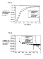
- the Schottky barrier diode of the third example of the present invention and that of the third comparative example have their respective current-voltage characteristics measured with direct-current voltage applied in the forward and reverse directions. A result thereof is shown in Table 2 and Figs. 5 and 6.
- Fig. 5 represents a relationship that each Schottky barrier diode in the third example exhibits between a forward voltage and a current as represented by density.
- the vertical axis represents the current as represented by density in A/cm -2
- the horizontal axis represents the voltage in V.
- Fig. 6 represents a relationship that each Schottky barrier diode in the third example exhibits between a reverse voltage and a current as represented by density.
- Fig. 5 represents a relationship that each Schottky barrier diode in the third example exhibits between a reverse voltage and a current as represented by density.
- the Schottky barrier diode of the third example of the present invention has an n type carrier density of at least 5 ⁇ 10 15 cm -3 , which falls within a sufficiently low density range, and in comparison with the third comparative example, exhibits an improved breakdown voltage when reverse voltage is applied. Furthermore, when forward voltage is applied, the third example of the present invention exhibits an on-resistance of substantially the same extent as the low on-resistance of the third comparative example.
- a Schottky barrier diode having a drift layer having a low n type carrier density of at least 5 ⁇ 10 15 cm -3 and at most 5 ⁇ 10 16 cm -3 can reduce loss and achieve high breakdown voltage.
- HEMT high electron mobility transistor
- HEMT shown in Fig. 7 is fabricated in accordance with the method of fabricating a Schottky barrier diode as described in the second embodiment.
- Fig. 7 is a schematic cross section of the HEMT of the fourth example of the present invention.
- an n type, 2 inch, sapphire substrate is prepared as a substrate 111. Furthermore, a c plane of the seed substrate is used as a plane at which a group III-V compound semiconductor is grown.
- the seed substrate is cleaned in an atmosphere of hydrogen at 1,050°C and 100 Torr.
- the temperature is decreased to 500°C, and at 100 Torr and with a ratio of a group V element-containing material to a group III element-containing material being a ratio of 1,600 to 1, a 30 nm thick GaN layer is grown as a buffer layer 112 by MOCVD.
- Undoped GaN layer 113 has a carrier density unmeasurable because of high resistance, and has an Si content of 5 ⁇ 10 15 cm -3 .
- Undoped AlGaN layer 114 has an n type carrier density of at most 1 ⁇ 10 16 cm -3 .
- Buffer layer 112, undoped GaN layer 113, and undoped AlGaN layer 114 are grown using a group III element-containing material, a group V element-containing material and carrier gas similar to those used in the first example of the present invention.
- the present invention in the fourth example provides a HEMT 110.
- a fourth comparative example provides a method of fabricating a HEMT that is basically similar in configuration to the method of the fourth example of the present invention, except that the step of growing (S20) is performed with the group III element-containing material (i.e., TMG containing 0.02 ppm of silicon), group V element-containing material and carrier gas as used in the method of producing a group III-V compound semiconductor described in the first comparative example.
- the group III element-containing material i.e., TMG containing 0.02 ppm of silicon
- group V element-containing material and carrier gas as used in the method of producing a group III-V compound semiconductor described in the first comparative example.
- the HEMT of the fourth comparative example has undoped GaN layer 113 having a carrier density unmeasurable because of high resistance, and an Si content of 5 ⁇ 10 16 cm -3 , and undoped AlGaN layer 114 having an n type carrier density of 1 ⁇ 10 16 cm -3 .
- the HEMT of the fourth example of the present invention and that of the fourth comparative example have their respective current-voltage characteristics measured with voltage applied, similarly as has been done in the third example, to measure buffer layer 112 for breakdown voltage in the reverse direction and for resistance in the forward direction.
- a result thereof is shown in Table 3:
- the HEMT of the fourth example of the present invention has undoped GaN layer 113 having a low Si content, and accordingly, has buffer layer 112 having a higher breakdown voltage, and a lower resistance in the forward direction than that in the fourth comparative example.
- the HEMTs of the fourth example of the present invention and the fourth comparative example have lattice defect or other impurity introduced therein to compensate for n type carrier density to provide undoped GaN layer 113 with a significantly low carrier density.
- the fourth example of the present invention employs highly pure TMG. This allows an undoped GaN layer 113 to have a reduced Si content, and accordingly, electron mobility can be raised and resistance in forward direction can be reduced.
- an undoped GaN layer can have a reduced carrier density, and a HEMT that has a buffer layer having an enhanced breakdown voltage and achieving reduced resistance in the forward direction can be fabricated.
- a fifth example the vertical transistor shown in Fig. 8 is fabricated in accordance with the method of fabricating a Schottky barrier diode as described in the second embodiment.
- Fig. 8 is a schematic cross section of the vertical transistor of the fifth example of the present invention.
- an n type, 2 inch, GaN substrate 121 is prepared. Furthermore, a c plane of the seed substrate is used as a plane at which a group III-V compound semiconductor is grown.
- Drift layer 123 has an n type carrier density of 1 ⁇ 10 16 cm -3 .
- photolithography is employed to form a resist pattern and thereafter ion injection is employed to introduce Mg as an electrically conductive impurity into drift layer 123 at a predetermined region at a well region 124 and Si at a source region 125 to provide well region 124 and source region 125.
- ion injection is employed to introduce Mg as an electrically conductive impurity into drift layer 123 at a predetermined region at a well region 124 and Si at a source region 125 to provide well region 124 and source region 125.
- Au and Ni are deposited on the film in layers to deposit a gate electrode 128 on the film.
- a resist pattern is formed by photolithography. With this resist pattern used as a mask, the Au and Ni deposited in layers and the film are partially etched away to form gate electrode 128 and insulation film 126.
- the present invention in the fifth example provides a vertical transistor 120.
- a fifth comparative example provides a method of fabricating a vertical transistor that is basically similar in configuration to the method of the fifth example of the present invention, except that the step of growing (S20) is performed with the group III element-containing material (i.e., TMG containing 0.02 ppm of the silicon used in the method of producing a group III-V compound semiconductor), group V element-containing material and carrier gas as used in the first comparative example.
- the group III element-containing material i.e., TMG containing 0.02 ppm of the silicon used in the method of producing a group III-V compound semiconductor
- the vertical transistor of the fifth comparative example has drift layer 123 having a carrier density of 5 ⁇ 10 16 cm -3 .
- the vertical transistor of the fifth example of the present invention and that of the fifth comparative example have their respective current-voltage characteristics measured with reverse voltage applied, similarly as has been done in the third example, to measure breakdown voltage. A result thereof is shown in Table 4: Table 4 Breakdown Voltage in Reverse Direction Fifth Example of the Present Invention 1,200 V Fifth Comparative Example 40 V
- the vertical transistor in the fifth example of the present invention has undoped GaN layer 113 having a low carrier density and accordingly has a higher breakdown voltage than that of the fifth comparative example.
- drift layer 123 can have a reduced carrier density, and a vertical transistor having an increased breakdown voltage can be fabricated.
- the light emitting diode shown in Fig. 3 is fabricated in accordance with the method of fabricating a light emitting diode as described in the third embodiment.
- an n type, 2 inch, GaN substrate is prepared. Furthermore, a c plane of the seed substrate is used as a plane at which a group III-V compound semiconductor is grown.
- the step of growing (S20) is performed at 1,150°C and 750 Torr with a ratio of a group V element-containing material to a group III element-containing material being a ratio of 1,100 to 1 to grow a 2 ⁇ m GaN layer as n type buffer layer 202 by MOCVD.
- the group III and V element-containing materials are similar to those used in the first example of the present invention.
- Carrier gases similar to those of the first example of the present invention, i.e., hydrogen and nitrogen, are used.
- Another material containing an n type impurity is monomethylsilane.
- N type buffer layer 202 has an n type carrier density of 3 ⁇ 10 18 cm -3 .
- active layer 203 is deposited. More specifically, at 780°C and 750 Torr and with a ratio of a group V element-containing material to a group III element-containing material being a ratio of 16,000 to 1, In 0.14 Ga 0.86 N of 3 nm and GaN of 15 nm are each deposited in six layers by MOCVD to provide a multiquantum well structure.
- the group III and V element-containing materials are similar to those used in the first example of the present invention. In is obtained from trimethylindium containing at most 0.01 ppm of silicon. A carrier gas of nitrogen is used.
- p type electron block layer 204 is deposited. More specifically, at 1,050°C and 750 Torr and with a ratio of a group V element-containing material to a group III element-containing material being a ratio of 7,200 to 1, p type Al 0.18 Ga 0.82 N of 20 nm in thickness is grown by MOCVD.
- the group III and V element-containing materials are similar to those used in the first example of the present invention.
- Al is obtained from trimethylaluminum containing at most 0.01 ppm of silicon.
- Another material containing a p type impurity is biscyclopentadienylmagnesium. Carrier gases of nitrogen and hydrogen are used.
- P type electron block layer 204 has a p type carrier density of 7 ⁇ 10 17 cm -3 .
- p type contact layer 205 is deposited. More specifically, at 1,100°C and 750 Torr and with a ratio of a group V element-containing material to a group III element-containing material being a ratio of 1,600 to 1, p type GaN of 50 nm in thickness is grown by MOCVD.
- the group III and V element-containing materials are similar to those used in the first example of the present invention.
- Another material containing a p type impurity is biscyclopentadienylmagnesium. Carrier gases of nitrogen and hydrogen are used.
- P type contact layer 205 has a p type carrier density of 1 ⁇ 10 18 cm -3 .
- a blue light emitting diode 200 of the sixth example of the present invention as shown in Fig. 3 is thus fabricated.
- a sixth comparative example provides a method of fabricating a light emitting diode that is basically similar in configuration to the method of the sixth example of the present invention, except that the step of growing (S20) is performed with the group III element-containing material (i.e., TMG containing 0.02 ppm of the silicon used in the method of producing a group III-V compound semiconductor), group V element-containing material and carrier gas as used in the first comparative example.
- the group III element-containing material i.e., TMG containing 0.02 ppm of the silicon used in the method of producing a group III-V compound semiconductor
- the sixth comparative example provides a p type electron block layer having a p type carrier density of 3 ⁇ 10 17 cm -3 and p type contact layer 205 having a p type carrier density of 7 ⁇ 10 17 cm -3 .
- a current is passed through the p and n type electrodes of each of the light emitting diodes of the sixth example of the present invention and the sixth comparative example, respectively, to evaluate their optical outputs.
- a seventh example it is confirmed how effective it is to use as a group III element-containing material of the present invention an organic metal containing at most 0.01 ppm of silicon to fabricate a laser diode.
- the laser diode shown in Fig. 4 is fabricated in accordance with the method of fabricating a laser diode as described in the fourth embodiment.
- an n type, 2 inch, GaN substrate is prepared. Furthermore, a c plane of the seed substrate is used as a plane at which a group III-V compound semiconductor is grown.
- the step of growing (S20) is performed at 1,150°C and 760 Torr with a ratio of a group V element-containing material to a group III element-containing material being a ratio of 5,100 to 1 to grow a 2.3 ⁇ m thick AlGaN layer as n type cladding layer 302 by MOCVD.
- the group III and V element-containing materials are similar to those used in the first example of the present invention.
- Al is obtained from trimethylaluminum containing at most 0.01 ppm of silicon. Carrier gases of nitrogen and hydrogen are used.
- Another material containing an n type impurity is monomethylsilane.
- N type cladding layer 302 has an n type carrier density of 2 ⁇ 10 18 cm -3 .
- undoped guide layer 303 is deposited. More specifically, at 800°C and 760 Torr with a ratio of a group V element-containing material to a group III element-containing material being a ratio of 22,000 to 1, In 0.02 Ga 0.98 N of 50 nm in thickness is grown by MOCVD.
- the group III and V element-containing materials are similar to those used in the first example of the present invention. In is obtained from trimethylindium containing at most 0.01 ppm of silicon. A carrier gas of nitrogen is used.
- Undoped guide layer 303 has an n type carrier density of 1 ⁇ 10 16 cm -3 .
- active layer 304 is deposited. More specifically, at 800°C and 760 Torr and with a ratio of a group V element-containing material to a group III element-containing material being a ratio of 13,000 to 1, In 0.08 Ga 0.92 N of 3 nm and In 0.01 Ga 0.99 N of 15 nm are each deposited in three layers by MOCVD to provide a multiquantum well structure.
- the group III and V element-containing materials are similar to those used in the first example of the present invention. In is obtained from trimethylindium containing at most 0.01 ppm of silicon. A carrier gas of nitrogen is used.
- undoped guide layer 305 is deposited. More specifically, at 1,100°C and 760 Torr with a ratio of a group V element-containing material to a group III element-containing material being a ratio of 2,300 to 1, GaN of 0.1 ⁇ m in thickness is grown by MOCVD.
- the group III and V element-containing materials are similar to those used in the first example of the present invention. Carrier gases of hydrogen and nitrogen are used.
- Undoped guide layer 305 has an n type carrier density of 1 ⁇ 10 16 cm -3 .
- p type electron block layer 306 is deposited. More specifically, at 1,100°C and 760 Torr and with a ratio of a group V element-containing material to a group III element-containing material being a ratio of 10,000 to 1, p type Al 0.18 Ga 0.82 N of 20 nm in thickness is grown by MOCVD.
- the group III and V element-containing materials are similar to those used in the first example of the present invention.
- Al is obtained from trimethylaluminum containing at most 0.01 ppm of silicon.
- Another material containing a p type impurity is biscyclopentadienylmagnesium. Carrier gases of nitrogen and hydrogen are used.
- P type electron block layer 306 has a p type carrier density of 5 ⁇ 10 17 cm -3 .
- p type cladding layer 307 is deposited. More specifically, at 1,100°C and 760 Torr and with a ratio of a group V element-containing material to a group III element-containing material being a ratio of 10,000 to 1, p type Al 0.07 Ga 0.93 N of 0.4 ⁇ m in thickness is grown by MOCVD.
- the group III and V element-containing materials are similar to those used in the first example of the present invention.
- Al is obtained from trimethylaluminum containing at most 0.01 ppm of silicon.
- Another material containing a p type impurity is biscyclopentadienylmagnesium. Carrier gases of nitrogen and hydrogen are used.
- P type cladding layer 307 has a p type carrier density of 7 ⁇ 10 17 cm -3 .
- p type contact layer 308 is deposited. More specifically, at 1,100°C and 760 Torr and with a ratio of a group V element-containing material to a group III element-containing material being a ratio of 3,300 to 1, p type GaN of 50 nm in thickness is grown by MOCVD.
- the group III and V element-containing materials are TMG similar to that used in the first example of the present invention.
- Another material containing a p type impurity is biscyclopentadienylmagnesium. Carrier gases of nitrogen and hydrogen are used.
- P type contact layer 308 has a p type carrier density of 1 ⁇ 10 18 cm -3 .
- a heat treatment is performed and that surface of substrate 301 which is opposite to the surface having n type cladding layer 302 deposited thereon is polished to be reduced in thickness.
- Ti and Al are deposited in layers to deposit n type electrode 310 on that surface of substrate 301 which is opposite to the surface having n type cladding layer 302 deposited thereon.
- Ni and Au are deposited in layers to deposit p type electrode 309 on p type contact layer 308.
- P type electrode 309 is processed to be a stripe having a width of 10 ⁇ m. Thereafter a bar having a cavity length of 800 ⁇ m is formed by cleavage.
- a blue-violet laser diode 300 of the seventh example of the present invention shown in Fig. 4 is thus fabricated.
- a seventh comparative example provides a method of fabricating a laser diode that is basically similar in configuration to the method of the seventh example of the present invention, except that the step of growing (S20) is performed with the group III element-containing material (i.e., TMG containing 0.02 ppm of the silicon used in the method of producing a group III-V compound semiconductor), group V element-containing material and carrier gas as used in the first comparative example.
- the group III element-containing material i.e., TMG containing 0.02 ppm of the silicon used in the method of producing a group III-V compound semiconductor
- an undoped guide layer deposited on an active layer has an n type carrier density of 5 ⁇ 10 16 cm -3 .
- a p type electron block layer has a p type carrier density of 3 ⁇ 10 17 cm -3 .
- P type cladding layer 307 has a p type carrier density of 5 ⁇ 10 17 cm -3 .
- P type contact layer 205 has a p type carrier density of 5 ⁇ 10 17 cm -3 .
- a current is passed through the p and n type electrodes of each of the laser diodes of the seventh example of the present invention and the seventh comparative example, respectively, to evaluate their optical outputs.
- the laser diode of the seventh example of the present invention provides a threshold current lower by 10% than that of the seventh comparative example, and a rate at which an output increases relative to a current after lasing, i.e., a slope efficiency, higher by 10% than that of the seventh comparative example.
Landscapes
- Chemical & Material Sciences (AREA)
- Engineering & Computer Science (AREA)
- Nanotechnology (AREA)
- Life Sciences & Earth Sciences (AREA)
- Optics & Photonics (AREA)
- Materials Engineering (AREA)
- Mechanical Engineering (AREA)
- Metallurgy (AREA)
- Organic Chemistry (AREA)
- Physics & Mathematics (AREA)
- General Chemical & Material Sciences (AREA)
- Biophysics (AREA)
- Chemical Kinetics & Catalysis (AREA)
- Crystallography & Structural Chemistry (AREA)
- Inorganic Chemistry (AREA)
- Led Devices (AREA)
- Semiconductor Lasers (AREA)
- Electrodes Of Semiconductors (AREA)
- Chemical Vapour Deposition (AREA)
- Crystals, And After-Treatments Of Crystals (AREA)
Applications Claiming Priority (1)
| Application Number | Priority Date | Filing Date | Title |
|---|---|---|---|
| JP2007104027A JP2008263023A (ja) | 2007-04-11 | 2007-04-11 | Iii−v族化合物半導体の製造方法、ショットキーバリアダイオード、発光ダイオード、レーザダイオード、およびそれらの製造方法 |
Publications (2)
| Publication Number | Publication Date |
|---|---|
| EP1981069A2 true EP1981069A2 (de) | 2008-10-15 |
| EP1981069A3 EP1981069A3 (de) | 2013-06-26 |
Family
ID=39591770
Family Applications (1)
| Application Number | Title | Priority Date | Filing Date |
|---|---|---|---|
| EP08003392.1A Withdrawn EP1981069A3 (de) | 2007-04-11 | 2008-02-25 | Verfahren zur Herstellung eines Gruppe-III-V-Verbindungshalbleiters, Schottky-Barrierendiode, Lichtemissionsdiode, Laserdiode und Herstellungsverfahren für die Dioden |
Country Status (6)
| Country | Link |
|---|---|
| US (1) | US20080251801A1 (de) |
| EP (1) | EP1981069A3 (de) |
| JP (1) | JP2008263023A (de) |
| KR (1) | KR20080092253A (de) |
| CN (1) | CN101311380B (de) |
| TW (1) | TWI381072B (de) |
Families Citing this family (16)
| Publication number | Priority date | Publication date | Assignee | Title |
|---|---|---|---|---|
| US7872285B2 (en) * | 2005-03-04 | 2011-01-18 | Sumitomo Electric Industries, Ltd. | Vertical gallium nitride semiconductor device and epitaxial substrate |
| CN102569557A (zh) * | 2007-07-17 | 2012-07-11 | 住友电气工业株式会社 | 电子器件的制作方法、外延衬底的制作方法、iii族氮化物半导体元件及氮化镓外延衬底 |
| US20090149008A1 (en) * | 2007-10-05 | 2009-06-11 | Applied Materials, Inc. | Method for depositing group iii/v compounds |
| US20110180133A1 (en) * | 2008-10-24 | 2011-07-28 | Applied Materials, Inc. | Enhanced Silicon-TCO Interface in Thin Film Silicon Solar Cells Using Nickel Nanowires |
| JP4375497B1 (ja) | 2009-03-11 | 2009-12-02 | 住友電気工業株式会社 | Iii族窒化物半導体素子、エピタキシャル基板、及びiii族窒化物半導体素子を作製する方法 |
| CN102449743A (zh) | 2009-04-24 | 2012-05-09 | 应用材料公司 | 用于后续高温第三族沉积的基材预处理 |
| TWI467635B (zh) * | 2011-02-17 | 2015-01-01 | Soitec Silicon On Insulator | 凹孔缺陷縮減之三五族半導體構造及形成此等構造之方法 |
| JP2012186195A (ja) * | 2011-03-03 | 2012-09-27 | Toshiba Corp | 半導体発光素子及びその製造方法 |
| JP5433609B2 (ja) | 2011-03-03 | 2014-03-05 | 株式会社東芝 | 半導体発光素子及びその製造方法 |
| KR20130014849A (ko) * | 2011-08-01 | 2013-02-12 | 삼성전자주식회사 | 쇼트키 배리어 다이오드 및 이의 제조방법 |
| US8946788B2 (en) | 2011-08-04 | 2015-02-03 | Avogy, Inc. | Method and system for doping control in gallium nitride based devices |
| KR101984698B1 (ko) | 2012-01-11 | 2019-05-31 | 삼성전자주식회사 | 기판 구조체, 이로부터 제조된 반도체소자 및 그 제조방법 |
| US11025029B2 (en) | 2015-07-09 | 2021-06-01 | International Business Machines Corporation | Monolithic III-V nanolaser on silicon with blanket growth |
| KR101996424B1 (ko) * | 2017-04-24 | 2019-07-04 | 아주대학교산학협력단 | 레이저 다이오드 및 그 제조 방법 |
| DE102019111598A1 (de) * | 2019-05-06 | 2020-11-12 | Aixtron Se | Verfahren zum Abscheiden eines Halbleiter-Schichtsystems, welches Gallium und Indium enthält |
| JP7380423B2 (ja) * | 2020-05-27 | 2023-11-15 | 豊田合成株式会社 | 半導体装置の製造方法 |
Citations (1)
| Publication number | Priority date | Publication date | Assignee | Title |
|---|---|---|---|---|
| JP2006342101A (ja) | 2005-06-09 | 2006-12-21 | Shin Etsu Chem Co Ltd | 有機金属化合物の製造方法 |
Family Cites Families (13)
| Publication number | Priority date | Publication date | Assignee | Title |
|---|---|---|---|---|
| JPS62132888A (ja) * | 1985-12-03 | 1987-06-16 | Sumitomo Chem Co Ltd | 有機金属化合物の精製方法 |
| US5573742A (en) * | 1987-10-29 | 1996-11-12 | Martin Marietta Corporation | Method for the preparation of high purity aluminum nitride |
| JP2001338886A (ja) * | 2000-03-24 | 2001-12-07 | Ngk Insulators Ltd | 半導体デバイス、その製造方法、及びそれに用いる半導体デバイス用基板 |
| EP1387453B1 (de) * | 2001-04-12 | 2009-11-11 | Nichia Corporation | Halbleiterelement aus galliumnitridzusammensetzung |
| CN1228478C (zh) * | 2002-11-13 | 2005-11-23 | 中国科学院物理研究所 | 制备氮化镓单晶薄膜的方法 |
| CN1242091C (zh) * | 2002-12-20 | 2006-02-15 | 上海北大蓝光科技有限公司 | Mocvd生长氮化物发光二极管结构外延片的方法 |
| JP2006001896A (ja) * | 2004-06-18 | 2006-01-05 | Shin Etsu Chem Co Ltd | 高純度トリメチルアルミニウム及びトリメチルアルミニウムの精製方法 |
| TWI375994B (en) * | 2004-09-01 | 2012-11-01 | Sumitomo Electric Industries | Epitaxial substrate and semiconductor element |
| TW200619222A (en) * | 2004-09-02 | 2006-06-16 | Rohm & Haas Elect Mat | Method for making organometallic compounds |
| US7390360B2 (en) * | 2004-10-05 | 2008-06-24 | Rohm And Haas Electronic Materials Llc | Organometallic compounds |
| JP4470682B2 (ja) * | 2004-10-13 | 2010-06-02 | 住友化学株式会社 | トリメチルガリウムの製造方法 |
| JP4984557B2 (ja) * | 2005-03-04 | 2012-07-25 | 住友電気工業株式会社 | 縦型窒化ガリウム半導体装置を作製する方法、エピタキシャル基板を作製する方法 |
| US7341932B2 (en) * | 2005-09-30 | 2008-03-11 | The United States Of America As Represented By The Administrator Of The National Aeronautics And Space Administration | Schottky barrier diode and method thereof |
-
2007
- 2007-04-11 JP JP2007104027A patent/JP2008263023A/ja active Pending
-
2008
- 2008-02-21 TW TW097106136A patent/TWI381072B/zh not_active IP Right Cessation
- 2008-02-25 EP EP08003392.1A patent/EP1981069A3/de not_active Withdrawn
- 2008-03-12 US US12/046,805 patent/US20080251801A1/en not_active Abandoned
- 2008-03-27 KR KR1020080028579A patent/KR20080092253A/ko not_active Ceased
- 2008-04-11 CN CN2008100871007A patent/CN101311380B/zh not_active Expired - Fee Related
Patent Citations (1)
| Publication number | Priority date | Publication date | Assignee | Title |
|---|---|---|---|---|
| JP2006342101A (ja) | 2005-06-09 | 2006-12-21 | Shin Etsu Chem Co Ltd | 有機金属化合物の製造方法 |
Also Published As
| Publication number | Publication date |
|---|---|
| CN101311380A (zh) | 2008-11-26 |
| TW200848559A (en) | 2008-12-16 |
| JP2008263023A (ja) | 2008-10-30 |
| TWI381072B (zh) | 2013-01-01 |
| KR20080092253A (ko) | 2008-10-15 |
| US20080251801A1 (en) | 2008-10-16 |
| CN101311380B (zh) | 2011-10-05 |
| EP1981069A3 (de) | 2013-06-26 |
Similar Documents
| Publication | Publication Date | Title |
|---|---|---|
| EP1981069A2 (de) | Verfahren zur Herstellung eines Gruppe-III-V-Verbindungshalbleiters, Schottky-Barrierendiode, Lichtemissionsdiode, Laserdiode und Herstellungsverfahren für die Dioden | |
| US9865719B2 (en) | Carbon doping semiconductor devices | |
| US5432808A (en) | Compound semicondutor light-emitting device | |
| US8835983B2 (en) | Nitride semiconductor device including a doped nitride semiconductor between upper and lower nitride semiconductor layers | |
| US9153648B2 (en) | Semiconductor stacked body, method for manufacturing same, and semiconductor element | |
| JP5099008B2 (ja) | SiC基板を用いた化合物半導体装置とその製造方法 | |
| US8106419B2 (en) | Group-III nitride compound semiconductor light-emitting device, method of manufacturing group-III nitride compound semiconductor light-emitting device, and lamp | |
| EP2086003A2 (de) | Wachstumsverfahren für einen Gruppe-III-V-Verbindungshalbleiter und Herstellungsverfahren für lichtemittierende Vorrichtung und elektronische Vorrichtung | |
| KR20120049371A (ko) | 질화물 반도체 소자 및 그 제조 방법 | |
| US10008571B2 (en) | Semiconductor wafer, semiconductor device, and method for manufacturing nitride semiconductor layer | |
| US20090072221A1 (en) | Nitride semiconductor device and method for fabricating the same | |
| US9401402B2 (en) | Nitride semiconductor device and nitride semiconductor substrate | |
| CN102239574A (zh) | 制造发光元件的方法和发光元件 | |
| US7462505B2 (en) | Growth process of a crystalline gallium nitride based compound and semiconductor device including gallium nitride based compound | |
| KR101125408B1 (ko) | 화합물 반도체 및 그 제조 방법 | |
| US9287441B2 (en) | Method for manufacturing semiconductor device | |
| KR102553985B1 (ko) | Ⅲ족 질화물 반도체 | |
| US20150263221A1 (en) | Semiconductor and Template for Growing Semiconductors | |
| JP2010028147A (ja) | Iii−v族化合物半導体の製造方法、ショットキーバリアダイオード、発光ダイオード、レーザダイオード、およびそれらの製造方法 |
Legal Events
| Date | Code | Title | Description |
|---|---|---|---|
| PUAI | Public reference made under article 153(3) epc to a published international application that has entered the european phase |
Free format text: ORIGINAL CODE: 0009012 |
|
| 17P | Request for examination filed |
Effective date: 20080225 |
|
| AK | Designated contracting states |
Kind code of ref document: A2 Designated state(s): AT BE BG CH CY CZ DE DK EE ES FI FR GB GR HR HU IE IS IT LI LT LU LV MC MT NL NO PL PT RO SE SI SK TR |
|
| AX | Request for extension of the european patent |
Extension state: AL BA MK RS |
|
| PUAL | Search report despatched |
Free format text: ORIGINAL CODE: 0009013 |
|
| AK | Designated contracting states |
Kind code of ref document: A3 Designated state(s): AT BE BG CH CY CZ DE DK EE ES FI FR GB GR HR HU IE IS IT LI LT LU LV MC MT NL NO PL PT RO SE SI SK TR |
|
| AX | Request for extension of the european patent |
Extension state: AL BA MK RS |
|
| RIC1 | Information provided on ipc code assigned before grant |
Ipc: H01L 21/205 20060101AFI20130523BHEP Ipc: H01L 21/02 20060101ALI20130523BHEP Ipc: H01L 29/872 20060101ALN20130523BHEP Ipc: C23C 16/30 20060101ALI20130523BHEP |
|
| AKY | No designation fees paid | ||
| REG | Reference to a national code |
Ref country code: DE Ref legal event code: R108 |
|
| REG | Reference to a national code |
Ref country code: DE Ref legal event code: R108 Effective date: 20140305 |
|
| STAA | Information on the status of an ep patent application or granted ep patent |
Free format text: STATUS: THE APPLICATION IS DEEMED TO BE WITHDRAWN |
|
| 18D | Application deemed to be withdrawn |
Effective date: 20140103 |