EP1978629B1 - Circuit de rectification et circuit de rectification triphase - Google Patents
Circuit de rectification et circuit de rectification triphase Download PDFInfo
- Publication number
- EP1978629B1 EP1978629B1 EP06834695.6A EP06834695A EP1978629B1 EP 1978629 B1 EP1978629 B1 EP 1978629B1 EP 06834695 A EP06834695 A EP 06834695A EP 1978629 B1 EP1978629 B1 EP 1978629B1
- Authority
- EP
- European Patent Office
- Prior art keywords
- phase
- chopper
- currents
- output ends
- diode bridge
- Prior art date
- Legal status (The legal status is an assumption and is not a legal conclusion. Google has not performed a legal analysis and makes no representation as to the accuracy of the status listed.)
- Not-in-force
Links
Images


Classifications
-
- H—ELECTRICITY
- H02—GENERATION; CONVERSION OR DISTRIBUTION OF ELECTRIC POWER
- H02M—APPARATUS FOR CONVERSION BETWEEN AC AND AC, BETWEEN AC AND DC, OR BETWEEN DC AND DC, AND FOR USE WITH MAINS OR SIMILAR POWER SUPPLY SYSTEMS; CONVERSION OF DC OR AC INPUT POWER INTO SURGE OUTPUT POWER; CONTROL OR REGULATION THEREOF
- H02M7/00—Conversion of ac power input into dc power output; Conversion of dc power input into ac power output
- H02M7/02—Conversion of ac power input into dc power output without possibility of reversal
- H02M7/04—Conversion of ac power input into dc power output without possibility of reversal by static converters
- H02M7/06—Conversion of ac power input into dc power output without possibility of reversal by static converters using discharge tubes without control electrode or semiconductor devices without control electrode
- H02M7/08—Conversion of ac power input into dc power output without possibility of reversal by static converters using discharge tubes without control electrode or semiconductor devices without control electrode arranged for operation in parallel
-
- H—ELECTRICITY
- H02—GENERATION; CONVERSION OR DISTRIBUTION OF ELECTRIC POWER
- H02M—APPARATUS FOR CONVERSION BETWEEN AC AND AC, BETWEEN AC AND DC, OR BETWEEN DC AND DC, AND FOR USE WITH MAINS OR SIMILAR POWER SUPPLY SYSTEMS; CONVERSION OF DC OR AC INPUT POWER INTO SURGE OUTPUT POWER; CONTROL OR REGULATION THEREOF
- H02M1/00—Details of apparatus for conversion
- H02M1/42—Circuits or arrangements for compensating for or adjusting power factor in converters or inverters
- H02M1/4208—Arrangements for improving power factor of AC input
- H02M1/4216—Arrangements for improving power factor of AC input operating from a three-phase input voltage
-
- H—ELECTRICITY
- H02—GENERATION; CONVERSION OR DISTRIBUTION OF ELECTRIC POWER
- H02M—APPARATUS FOR CONVERSION BETWEEN AC AND AC, BETWEEN AC AND DC, OR BETWEEN DC AND DC, AND FOR USE WITH MAINS OR SIMILAR POWER SUPPLY SYSTEMS; CONVERSION OF DC OR AC INPUT POWER INTO SURGE OUTPUT POWER; CONTROL OR REGULATION THEREOF
- H02M1/00—Details of apparatus for conversion
- H02M1/42—Circuits or arrangements for compensating for or adjusting power factor in converters or inverters
- H02M1/4208—Arrangements for improving power factor of AC input
- H02M1/4225—Arrangements for improving power factor of AC input using a non-isolated boost converter
-
- H—ELECTRICITY
- H02—GENERATION; CONVERSION OR DISTRIBUTION OF ELECTRIC POWER
- H02M—APPARATUS FOR CONVERSION BETWEEN AC AND AC, BETWEEN AC AND DC, OR BETWEEN DC AND DC, AND FOR USE WITH MAINS OR SIMILAR POWER SUPPLY SYSTEMS; CONVERSION OF DC OR AC INPUT POWER INTO SURGE OUTPUT POWER; CONTROL OR REGULATION THEREOF
- H02M3/00—Conversion of dc power input into dc power output
- H02M3/02—Conversion of dc power input into dc power output without intermediate conversion into ac
- H02M3/04—Conversion of dc power input into dc power output without intermediate conversion into ac by static converters
- H02M3/10—Conversion of dc power input into dc power output without intermediate conversion into ac by static converters using discharge tubes with control electrode or semiconductor devices with control electrode
- H02M3/145—Conversion of dc power input into dc power output without intermediate conversion into ac by static converters using discharge tubes with control electrode or semiconductor devices with control electrode using devices of a triode or transistor type requiring continuous application of a control signal
- H02M3/155—Conversion of dc power input into dc power output without intermediate conversion into ac by static converters using discharge tubes with control electrode or semiconductor devices with control electrode using devices of a triode or transistor type requiring continuous application of a control signal using semiconductor devices only
- H02M3/156—Conversion of dc power input into dc power output without intermediate conversion into ac by static converters using discharge tubes with control electrode or semiconductor devices with control electrode using devices of a triode or transistor type requiring continuous application of a control signal using semiconductor devices only with automatic control of output voltage or current, e.g. switching regulators
-
- H—ELECTRICITY
- H02—GENERATION; CONVERSION OR DISTRIBUTION OF ELECTRIC POWER
- H02M—APPARATUS FOR CONVERSION BETWEEN AC AND AC, BETWEEN AC AND DC, OR BETWEEN DC AND DC, AND FOR USE WITH MAINS OR SIMILAR POWER SUPPLY SYSTEMS; CONVERSION OF DC OR AC INPUT POWER INTO SURGE OUTPUT POWER; CONTROL OR REGULATION THEREOF
- H02M7/00—Conversion of ac power input into dc power output; Conversion of dc power input into ac power output
- H02M7/02—Conversion of ac power input into dc power output without possibility of reversal
- H02M7/04—Conversion of ac power input into dc power output without possibility of reversal by static converters
- H02M7/12—Conversion of ac power input into dc power output without possibility of reversal by static converters using discharge tubes with control electrode or semiconductor devices with control electrode
-
- H—ELECTRICITY
- H02—GENERATION; CONVERSION OR DISTRIBUTION OF ELECTRIC POWER
- H02M—APPARATUS FOR CONVERSION BETWEEN AC AND AC, BETWEEN AC AND DC, OR BETWEEN DC AND DC, AND FOR USE WITH MAINS OR SIMILAR POWER SUPPLY SYSTEMS; CONVERSION OF DC OR AC INPUT POWER INTO SURGE OUTPUT POWER; CONTROL OR REGULATION THEREOF
- H02M5/00—Conversion of ac power input into ac power output, e.g. for change of voltage, for change of frequency, for change of number of phases
- H02M5/02—Conversion of ac power input into ac power output, e.g. for change of voltage, for change of frequency, for change of number of phases without intermediate conversion into dc
- H02M5/04—Conversion of ac power input into ac power output, e.g. for change of voltage, for change of frequency, for change of number of phases without intermediate conversion into dc by static converters
- H02M5/10—Conversion of ac power input into ac power output, e.g. for change of voltage, for change of frequency, for change of number of phases without intermediate conversion into dc by static converters using transformers
- H02M5/14—Conversion of ac power input into ac power output, e.g. for change of voltage, for change of frequency, for change of number of phases without intermediate conversion into dc by static converters using transformers for conversion between circuits of different phase number
-
- Y—GENERAL TAGGING OF NEW TECHNOLOGICAL DEVELOPMENTS; GENERAL TAGGING OF CROSS-SECTIONAL TECHNOLOGIES SPANNING OVER SEVERAL SECTIONS OF THE IPC; TECHNICAL SUBJECTS COVERED BY FORMER USPC CROSS-REFERENCE ART COLLECTIONS [XRACs] AND DIGESTS
- Y02—TECHNOLOGIES OR APPLICATIONS FOR MITIGATION OR ADAPTATION AGAINST CLIMATE CHANGE
- Y02B—CLIMATE CHANGE MITIGATION TECHNOLOGIES RELATED TO BUILDINGS, e.g. HOUSING, HOUSE APPLIANCES OR RELATED END-USER APPLICATIONS
- Y02B70/00—Technologies for an efficient end-user side electric power management and consumption
- Y02B70/10—Technologies improving the efficiency by using switched-mode power supplies [SMPS], i.e. efficient power electronics conversion e.g. power factor correction or reduction of losses in power supplies or efficient standby modes
Definitions
- the present invention relates to rectification techniques, and particularly to a field called multiple rectification.
- Non-Patent Documents 1 and 2 and Patent Document 1 These schemes adopt a technique called multiple rectification, and Non-Patent Documents 1 and 2 disclose techniques in which each of polyphase currents generates 12 pulses in one period, and two rectifier circuits are connected in parallel to the load (this technique is hereinafter referred to as "12-pulse rectification”). Also, Patent Document 1 discloses a technique in which each of polyphase currents generates 18 pulses in one period, and three rectifier circuits are connected in parallel to the load (this technique is hereinafter referred to as "18-pulse rectification"). Adopting these techniques eliminates the fifth, seventh, or eleventh, thirteenth harmonic components.
- Non-Patent Document 2 provides an additional coil to an interphase reactor connecting the outputs of two rectifier circuits together, in order to improve the current waveform in 12-pulse rectification. Alternating current is applied to the coil, so as to inject a current into the interphase reactor. This improves the current waveform inputted to the transformer for obtaining the 12 pulses of current.
- Non-Patent Document 2 injecting a current into an interphase reactor with an additional coil, as described in Non-Patent Document 2, requires applying a complicated waveform to the coil.
- Non-Patent Document 2 avoids such a complicated waveform, and applies a triangular wave to the coil, but then distortion remains in the input current as a natural result.
- the device for injecting current into the interphase reactor is configured complicatedly, or a separate voltage source is required.
- Patent Document 1 Japanese Patent Laid Open No. 59-15475 (1984 )
- Non-Patent Document 1 Hisao Matsumoto, "Twelve-pulse Converter with Autotransformer Connection", The Institute of Electrical Engineers of Japan, Transactions B, vol. 96, no. 8, pp. 406-412
- Non-Patent Document 2 Sewan Choi, P.N. Enjeti, H. Lee and I.L. Pitel: "A new active interphase reactor for 12-pulse rectifiers provides clean power utility interface", IEEE Trans. Ind. Applicat., vol. 32, no. 6, pp. 1304-1311 (1996 )
- Non-Patent Document 3 Takao Hirasa, "Power Electronics”, Kyoritsu Shuppan Co., Ltd, pp. 77-90, 1992
- US 2004/0202012 A1 is directed to yet another regulated AC to DC converter, comprising an input transformer for three-phase AC power and dividing a phase shifted AC power into two channels, to 6-pulse rectifiers, for each of the channels, switching converter and step down transformer in a channel, as well as an output rectifier of the channels.
- the present invention has been made by considering the problems above, and an object of the present invention is to provide a technique by which currents flowing in a transformer for outputting plural sets of three-phase currents given to a multiple rectifier circuit are easily made close to sinusoidal waves.
- a rectifier circuit comprises the features of claim 1. Further aspects are disclosed in the dependent claims.
- the rectifier circuit of the first aspect further comprises an interphase reactor (71) which is connected to said input ends of said first three-phase diode bridge (31) and in which the currents (i u1 , i v1 , i w1 ) inputted to said input ends flow.
- the rectifier circuit of the first aspect or the second aspect further comprises an interphase reactor (72) which is connected between said first three-phase diode bridge and said first chopper and in which said first rectified current (i d1 ) flows.
- said first chopper (43) comprises: a first inductor (411) in which said first rectified current (i d1 ) flows; a first diode (413) having an anode connected to said one (31P) of said output ends of said first three-phase diode bridge (31) through said first inductor, and a cathode connected to one (43P) of said output ends of said first chopper; a second inductor (431) connected to the other (31N) of said output ends of said first three-phase diode bridge; a second diode (434) having a cathode connected to said other (31N) of said output ends of said first three-phase diode bridge through said second inductor, and an anode connected to the other (43N) of said output ends of said first chopper; and a switching element (412) having a first end connected to the anode of said first dio
- Said second chopper (44) comprises: a third inductor (421) in which said second rectified current (i d2 ) flows; a third diode (423) having an anode connected to said one (32P) of said output ends of said second three-phase diode bridge (32) through said third inductor, and a cathode connected to one (44P) of said output ends of said second chopper; a fourth inductor (441) connected to the other (32N) of said output ends of said second three-phase diode bridge; a fourth diode (444) having a cathode connected to said other (32N) of said output ends of said second three-phase diode bridge through said fourth inductor, and an anode connected to the other (44N) of said output ends of said second chopper; and a switching element (422) having a first end connected to the anode of said third diode and a second end connected to the cathode of said fourth diode, said switching element opening
- said first chopper and said second chopper are both step-up choppers.
- said first chopper operation is controlled by pulse width modulation on the basis of a first modulation wave having a carrier frequency
- said second chopper operation is controlled by pulse width modulation on the basis of a second modulation wave having said carrier frequency and being in opposite phase to said first modulation wave.
- the rectifier circuit of any of the first to sixth aspects further comprises a smoothing capacitor (5) connected in parallel to said output ends of said first chopper and said output ends of said second chopper.
- the waveform of each of said first three-phase alternating currents and said second three-phase alternating currents exhibits a triangular wave in said first to fourth sections.
- the waveform of each of said first three-phase alternating currents and said second three-phase alternating currents exhibits a waveform formed by combining a curve that is similar to a waveform that a sinusoidal wave exhibits from 0 degree to 30 degrees and a waveform that is left-right symmetrical to the curve.
- a three-phase rectifier device comprises: the rectifier circuit according to any of the first to tenth aspects of the present invention; and a three-phase transformer (2) that receives three-phase currents (i u , i v , i w ), a fundamental frequency of said three-phase currents is a second value that is 1/6 of said first value and said three-phase currents having mutual phase differences of 120 degrees at the fundamental frequency, and that outputs first three-phase alternating currents (i u1 , i v1 , i w1 ) having phase differences of 15 degrees at the fundamental frequency respectively from said three-phase currents, and that also outputs second three-phase alternating currents (i u2 , i v2 , i w2 ) having phase differences of 30 degrees at the fundamental frequency from said first three-phase alternating currents.
- said three-phase transformer (2) comprises three autotransformers (21, 22, 23) each having a primary winding (211, 221, 232) and a secondary winding (212, 222, 232) coupled with said primary winding and having a center tap, said primary windings of said three autotransformers are delta-connected, and said center tap of each said autotransformer is connected to a connection point (U, V, W) that connects a pair of said primary windings other than said primary winding coupled with said secondary winding to which said center tap belongs.
- said three-phase transformer (2) comprises: three primary windings (211, 221, 231) corresponding to respective phases; and three secondary windings (212, 222, 232) coupled with all of said primary windings and each having a center tap, and wherein said primary windings are delta-connected, and said three center taps are individually connected to three connection points (U, V, W) at which a pair of said primary windings are connected together.
- the rectifier circuit of the present invention when a smoothing capacitor is connected in parallel to the pair of output ends of the first chopper and the pair of output ends of the second chopper, and first three-phase alternating currents having a fundamental frequency of a second value that is 1/6 of the first value are provided to the first three-phase diode bridge, and second three-phase alternating currents having phase differences of 30 degrees from the first three-phase alternating currents are provided to the second three-phase diode bridge, then the currents flowing in the transformer for outputting the first and second three-phase alternating currents is made close to sinusoidal waves. Also, the dc component of voltage can be controlled easily because the control is performed by using choppers.
- the rectifier circuit of the present invention even when a neutral point corresponding to the first three-phase alternating currents and a neutral point corresponding to the second three-phase alternating currents are not insulated and zero-phase voltage having a fundamental frequency of a third value that is 1/2 of the first value is generated, it is possible to suppress current flowing on the basis of the zero-phase voltage.
- the dc component of voltage is controlled, and dc voltage higher than the peak value of the power-supply voltage is obtained.
- ripple having the carrier frequency is reduced.
- the output voltage is smoothed.
- the first aspect to the third aspect of the three-phase rectifier device of the present invention it is possible to provide appropriate inputs respectively to the first three-phase diode bridge and the second three-phase diode bridge.
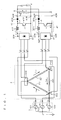
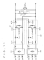
- FIG. 1 is a circuit diagram used to describe a first preferred embodiment of the present invention.
- a first three-phase diode bridge 31, a second three-phase diode bridge 32, a first chopper 41, and a second chopper 42 constitute a rectifier circuit.
- the rectifier circuit may be grasped as including a smoothing capacitor 5.
- a three-phase transformer 2 constitutes a three-phase rectifier device together with the rectifier circuit.
- the three-phase transformer 2 receives three-phase currents i u , i v , i w from a three-phase power supply 1, and outputs first three-phase alternating currents i u1 , i v1 , i w1 and second three-phase alternating currents i u2 , i v2 , i w2 .
- the three-phase power supply 1 includes a U-phase power supply 101, a V-phase power supply 102, and a W-phase power supply 103, respectively generating three-phase voltages e u , e v , e w .
- the U-phase power supply 101, the V-phase power supply 102, and the W-phase power supply 103 respectively supply the three-phase currents i u , i v , i w .
- the first three-phase diode bridge 31 receives the three-phase currents i u1 , i v1 , i w1 , and outputs a first rectified current i d1 .
- the second three-phase diode bridge 32 receives the three-phase currents i u2 , i v2 , i w2 , and outputs a second rectified current i d2 .
- FIG. 2 is a circuit diagram illustrating the configuration of the first three-phase diode bridge 31.
- the first three-phase diode bridge 31 has input ends 31U, 31V, 31W and output ends 31P and 31N. It applies full-wave rectification to the currents inputted to the input ends 31U, 31V, 31W, and outputs the first rectified current i d1 from the output end 31P.
- the three-phase currents i u1 , i v1 , i w1 are inputted to the input ends 31U, 31V, 31W.
- FIG. 3 is a circuit diagram illustrating the configuration of the second three-phase diode bridge 32.
- the second three-phase diode bridge 32 has input ends 32U, 32V, 32W and output ends 32P and 32N. It applies full-wave rectification to the currents inputted to the input ends 32U, 32V, 32W, and outputs the second rectified current i d2 from the output end 32P.
- the three-phase currents i u2 , i v2 , i w2 are inputted to the input ends 32U, 32V, 32W.
- the first chopper 41 performs a first chopper operation to receive the first rectified current i d1 as a current whose fundamental frequency has a first value. Then it outputs part of the first rectified current i d1 as a first chopper current i c1 .
- the second chopper 42 performs a second chopper operation to receive the second rectified current i d2 as a current whose fundamental frequency has the first value. Then it outputs part of the second rectified current i d2 as a second chopper current i c2 .
- the first chopper 41 and the second chopper 42 are step-up choppers.
- the first chopper 41 has output ends 41P and 41N, and outputs the first chopper current i c1 from the output end 41P.
- the first chopper 41 has an inductor 411 that is connected to the output end 31P of the first three-phase diode bridge 31 and receives the first rectified current i d1 .
- the collector of an insulated gate bipolar transistor (IGBT) 412 and the anode of a diode 413 are connected in common, and connected to the output end 31P through the inductor 411.
- the cathode of the diode 413 is connected to the output end 41P.
- the output ends 31N and 41N are connected in common to the emitter of the IGBT 412.
- the IGBT 412 functions as a switching element that opens/closes between its collector and emitter.
- the second chopper 42 includes output ends 42P and 42N, an inductor 421, an IGBT 422, and a diode 423, and the second chopper 42 outputs the second chopper current i c2 from the output end 42P.
- the output ends 41P and 41N are connected in parallel to the output ends 42P and 42N, and also in parallel to the smoothing capacitor 5.
- a load 6 is connected in parallel to the smoothing capacitor 5, and supplied with the both-end voltage v dc of the smoothing capacitor 5.
- the first chopper 41 and the second chopper 42 have their output ends connected in parallel with the smoothing capacitor 5, and so the current of the first chopper current i c1 and the second chopper current i c2 are continuous to function as a current source. Also, by adopting step-up type as the first chopper 41 and the second chopper 42, it is possible to obtain dc voltage that is higher than the peak values of the three-phase voltages e u , e v , e w . Also, by providing the smoothing capacitor 5, it is possible to smooth the output voltage.
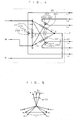
- FIG. 4 is a circuit diagram illustrating the details of the three-phase transformer 2, which is illustrated in Non-Patent Document 1, for example.
- the three-phase transformer 2 includes three autotransformers 21, 22, 23.
- the autotransformer 21 has a primary winding 211 connected between a U-phase input end U and a W-phase input end W, and a secondary winding 212 coupled with it and having a center tap.
- the secondary winding 212 is divided into secondary windings 2121 and 2122 by the center tap.
- the center tap is connected to a V-phase input end V.
- the autotransformer 22 has a primary winding 221 connected between the U-phase input end U and the V-phase input end V, and a secondary winding 222 coupled with it and having a center tap.
- the secondary winding 222 is divided into secondary windings 2221 and 2222 by the center tap.
- the center tap is connected to the W-phase input end W. While the number of turns of the primary winding 221 is n 1 , the number of turns of both of the secondary windings 2221 and 2222 is n 2 .
- the autotransformer 23 has a primary winding 231 connected between the W-phase input end W and the V-phase input end V, and a secondary winding 232 coupled with it and having a center tap.
- the secondary winding 232 is divided into secondary windings 2321 and 2322 by the center tap.
- the center tap is connected to the U-phase input end U. While the number of turns of the primary winding 231 is n 1 , the number of turns of both of the secondary windings 2321 and 2322 is n 2 .
- the primary windings 211, 221 and 231 are delta-connected.
- the three-phase currents i u , i v , i w from the three-phase power supply 1 flow respectively into the U-phase input end U, the V-phase input end V, and the W-phase input end W.
- a current i uw flows in the primary winding 211 from the W-phase input end W to the U-phase input end U
- a current i vu flows in the primary winding 221 from the U-phase input end U to the V-phase input end V
- a current i wv flows in the primary winding 231 from the V-phase input end V to the W-phase input end W.
- the currents i v1 and i v2 are outputted from the center tap of the secondary winding 212 respectively through the secondary windings 2121 and 2122, the currents i w1 and i w2 are outputted from the center tap of the secondary winding 222 respectively through the secondary windings 2221 and 2222, and the currents i u1 and i u2 are outputted from the center tap of the secondary winding 232 respectively through the secondary windings 2321 and 2322. Accordingly, Expression (3) holds.
- FIG. 5 is a phasor diagram illustrating the voltages in individual parts of the three-phase transformer 2, which is illustrated in Non-Patent Document 1.
- the three-phase voltages e u , e v , e w have phase differences of 120 degrees relative to each other, and the phase lags in this order.
- the voltage e u1 on the side opposite to the center tap of the secondary winding 2321 leads in phase by 15 degrees with respect to the voltage e u
- the voltage e v1 on the side opposite to the center tap of the secondary winding 2121 leads in phase by 15 degrees with respect to the voltage e v
- the voltage e w1 on the side opposite to the center tap of the secondary winding 2221 leads in phase by 15 degrees with respect to the voltage e w .
- the voltage e u2 on the side opposite to the center tap of the secondary winding 2322 lags in phase by 15 degrees with respect to the voltage e u
- the voltage e v2 on the side opposite to the center tap of the secondary winding 2122 lags in phase by 15 degrees with respect to the voltage e v
- the voltage e w2 on the side opposite to the center tap of the secondary winding 2222 lags in phase by 15 degrees with respect to the voltage e w .
- the absolute value E 1 of the voltage applied to the primary winding 231 is the absolute value of the difference between the voltage e v and the voltage e w , and a voltage having an absolute value a ⁇ E 1 is excited in the secondary winding 2322. Accordingly, because its center tap is connected to the U-phase input end U and the voltage e u is applied, the absolute value E t of the difference between the voltage e u2 and the voltage e u is equal to the absolute value a ⁇ E 1 . The same is true for the other phases.
- Such voltage relations are determined by the relative coupling and connection of the autotransformers 21, 22 and 23. Accordingly, as long as the three-phase voltages e u , e v , e w are stable, the voltage relations are maintained regardless of the waveforms of the currents i u1 , i v1 , i w1 , i u2 , i v2 , i w2 . In other words, by controlling the current waveforms, there is room to improve the waveforms of the three-phase currents i u , i v , i w inputted to the three-phase transformer 2 from the three-phase power supply 1.
- the currents i u1 , i v1 , i w1 , i u2 , i v2 , i w2 can be controlled on the basis of how they are inputted with the operations of the first chopper 41 and the second chopper 42.
- FIG. 6 is a graph illustrating a desired waveform i( ⁇ ) of the currents i u1 , i v1 , i w1 , i u2 , i v2 , i w2 .
- the phase of the angle ⁇ differs depending on the six currents.
- the waveform i( ⁇ ) is represented by Expression (4).
- Expression (5) is obtained by applying Fourier expansion to Expression (4).
- the waveform i( ⁇ ) has a fundamental component of cos ⁇ , and the components of even order, (3n)th, (12n+1)th, and (12n-1)th are zero. Accordingly, it is seen that the main harmonic components are (6m+1)th and (6m-1)th, with an odd number m.
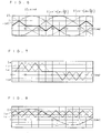
- FIG. 7 is a graph illustrating the currents i u1 and i u2 .
- the graph is based on the phase of the voltage e u .
- the minimum value of each is -I d and the maximum value is I d .
- the currents i u1 and i u2 respectively lead in phase by 15 degrees and lag in phase by 15 degrees.
- the currents i u1 , i v1 , i w1 have phase differences of 120 degrees with each other, and the currents i u2 , i v2 , i w2 have phase differences of 120 degrees with each other.
- FIG. 8 is a graph illustrating the waveforms of the first rectified current i d1 and the second rectified current i d2 together with the voltage e u .
- the first rectified current i d1 is obtained by applying full-wave rectification to the currents i u1 , i v1 , i w1 , and so it exhibits an approximately triangular wave that repeats in periods of 60 degrees in terms of the fundamental frequency of the voltage e u .
- the fundamental frequency of the three-phase alternating currents i u1 , i v1 , i w1 inputted to the input ends 31U, 31V, 31W of the first three-phase diode bridge 31 is 1/6 of the fundamental frequency of the first rectified current i d1 .
- the currents i u1 , i v1 , i w1 have the waveforms shown by Expression (6), and so the waveform of the first rectified current i d1 in a rising region exhibits a sine ⁇ waveform in the section of 0 ⁇ /6, and the waveform in a falling region exhibits a sine ⁇ waveform in the section of 5 ⁇ /6 ⁇ . That is, it exhibits a waveform formed by combining a curve that is similar to the waveform that a sinusoidal wave exhibits from 0 degree to 30 degrees and a waveform that is left-right symmetrical to the curve. The same is true for the second rectified current i d2 .
- a near triangular waveform configured on the basis of a waveform commonly called "middle-phase", not a maximum phase nor a minimum phase of a sinusoidal wave, is herein referred to as a three-phase ac middle-phase waveform.
- FIG. 9 is a graph illustrating the waveform obtained by obtaining the current i wv from Expressions (2) and (6).
- FIG. 10 is a graph illustrating the waveforms of currents (i u1 +i u2 ), (-i uw +i vu ), i u obtained from Expressions (2), (3), (6) and (7).
- the rectified currents i d1 and i d2 are close to a triangular wave, and so it is possible to receive these currents respectively from the three-phase diode bridges 31 and 32, with the chopper operations of the choppers 41 and 42. It is thus possible to input the currents i u1 , i v1 , i w1 , i u2 , i v2 , i w2 from the three-phase transformer 2 to the three-phase diode bridges 31 and 32, and it is possible for the three-phase transformer 2 to remove harmonic components of the currents i u , i v , i w .
- FIG. 11 is a circuit diagram illustrating parts of the configuration shown in FIG. 1 , showing parts for obtaining parameters on which the control of the chopper operations is based. Specifically, the values of the rectified currents i d1 and i d2 flowing respectively through the inductors 411 and 421 are detected respectively as data I d1 and data I d2 , and the value of the both-end voltage v dc of the smoothing capacitor 5 is detected as data V dc .
- Signals T1 and T2 for controlling the turning on/off of the IGBTs 412 and 422 are given to the gates of the IGBTs 412 and 422 through the buffers shown with triangular signs in the diagram.
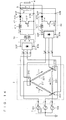
- FIG. 12 is a circuit diagram illustrating a configuration for generating the signals T1 and T2 on the basis of the data I d1 , I d2 , and V dc .
- This configuration can be roughly divided into a voltage control block 81, a current command generating block 82, a current control block 83, and a PWM modulation block 84.
- a voltage command generator 801 obtains a voltage command value V dc * corresponding to a desired both-end voltage V dc , which is inputted to the voltage control block 81 together with the data V dc .
- an operator 802 obtains a difference between the voltage command value V dc * and the data V dc , which is outputted to the current command generating block 82 through the processings in a PI controller 803 and a limiter 804.
- the current command generating block 82 includes waveform generators 805 and 806 for generating three-phase ac middle-phase waveforms, both of which generate a three-phase ac middle-phase waveform.
- the waveforms generated by the waveform generators 805 and 806 are in opposite phase to each other.
- FIG. 12 shows this opposite phase relation with the circles located in different positions near the waveform generators 805 and 806 (this sign does not indicate the inversion of polarity).
- the three-phase ac middle-phase waveforms generated by the waveform generators 805 and 806 have a frequency that is six times the fundamental frequency of the three-phase voltages e u , e v , e w (accordingly, of the currents i u1 , i v1 , i w1 , i u2 , i v2 , i w2 ), and so they can be grasped as having a mutual phase difference of 30 degrees, with reference to the fundamental frequency.
- the output of the voltage command generator 801 is inputted to a multiplier 807 and multiplied with the output of the waveform generator 805.
- the output of the voltage command generator 801 is inputted to a multiplier 808 and multiplied with the output of the waveform generator 806.
- the results of multiplication are outputted to the current control block 83 respectively as current command values I d1 * and I d2 * about the rectified currents i d1 and i d2 .
- an operator 809 obtains a difference between the current command value I d1 * and the data I d1 , which is outputted to the PWM modulation block 84 through the processing in a PI controller 810.
- an operator 811 obtains a difference between the current command value I d2 * and the data I d2 , which is outputted to the PWM modulation block 84 through the processing in a PI controller 812.
- the PWM modulation block 84 includes a carrier generator 813 for generating a modulation carrier C and differential amplifiers 815 and 816.
- the differential amplifier 815 is provided with the modulation carrier C and the output of the PI controller 810, and generates the signal T1.
- the differential amplifier 816 is provided with the modulation carrier C and the output of the PI controller 812, and generates the signal T2.
- the signals T1 and T2 control on/off of the IGBTs 412 and 422 such that rectified currents i d1 and i d2 corresponding to the current command values I d1 * and I d2 * flow and a both-end voltage V dc corresponding to the voltage command value V dc * is generated in the smoothing capacitor 5, whereby the operations of the choppers 41 and 42 are controlled.
- FIG. 13 is a circuit diagram used to describe a second preferred embodiment of the present invention.
- the configuration illustrated here differs from the configuration of the first preferred embodiment in that an interphase reactor 71 is additionally interposed between the three-phase transformer 2 and the first three-phase diode bridge 31.
- the input ends 31U, 31V, 31W of the first three-phase diode bridge 31 are connected respectively to the secondary windings 2321, 2121, 2221, each through one interphase reactor. That is, the three-phase currents i u1 , i v1 , i w1 flow in the interphase reactor 71.
- zero-phase voltage is generally generated between a neutral point on the input side of a three-phase diode bridge and an intermediate potential on the output side.
- This voltage is a triple component of the fundamental frequency of the three-phase voltage on the input side.
- zero-phase voltage is generated at a frequency of 1/2 of the fundamental frequency of the first rectified current i d1 , between the neutral point potential of the three-phase voltages e u1 , e v1 , e w1 given respectively to the input ends 31U, 31V, 31W and the intermediate potential of the voltage applied between the output ends 31P and 31N.
- Zero-phase voltage is similarly generated in the second three-phase diode bridge 32.
- zero-phase current current due to the zero-phase voltage is generated (hereinafter referred to as "zero-phase current"). This is because the three-phase currents become unbalanced with the generation of zero-phase voltage.
- the three-phase transformer 2 adopts the autotransformers 21, 22 and 23, and so the neutral points of the three-phase voltages e u1 , e v1 , e w1 and the three-phase voltages e u2 , e v2 , e w2 (see FIG. 5 ) respectively corresponding to the three-phase currents i u1 , i v1 , i w1 and the three-phase currents i u2 , i v2 , i w2 are common.
- FIG. 14 is a circuit diagram illustrating a modification of this preferred embodiment, where an interphase reactor 72 is provided between the first three-phase diode bridge 31 and the first chopper 41.
- the first rectified current i d1 flows through the interphase reactor 72. More specifically, the first rectified current i d1 flows in a reactor interposed between the output end 31P of the first three-phase diode bridge 31 and the inductor 411 of the first chopper 41.
- a reactor is provided also between the output end 31N of the first three-phase diode bridge 31 and the emitter of the IGBT 412.
- interphase reactor 72 located in this position because it cuts the zero-phase current in the same way as the interphase reactor 71.
- interphase reactors 71 and 72 described above are both provided for the first three-phase diode bridge 31, but they may be provided for the second three-phase diode bridge 32 on its input side or output side.
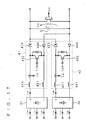
- FIG. 15 is a circuit diagram used to describe a third preferred embodiment of the present invention.
- the configuration shown here differs from the configuration of the first preferred embodiment in that the first chopper 41 and the second chopper 42 are replaced respectively by a first chopper 43 and a second chopper 44.
- the first chopper 43 additionally includes an inductor 431 and a diode 434. More specifically, the inductor 431 is interposed between the output end 31N of the first three-phase diode bridge 31 and the emitter of the IGBT 412. Also, the diode 434 has its anode connected to the output end 43N, and its cathode connected to the emitter of the IGBT 412.
- the second chopper 44 includes an inductor 441 and a diode 444 that are connected in the same way as the inductor 431 and the diode 434.
- ripple due to the modulation carrier C is superimposed on the rectified currents i d1 and i d2 .
- this preferred embodiment describes a scheme for reducing the ripple due to the carrier C.
- FIG. 16 is a circuit diagram illustrating a configuration adopted in this preferred embodiment and for generating the signals T1 and T2 on the basis of the data I d1 , I d2 and V dc .
- the differential amplifier 816 of this preferred embodiment is provided not with the carrier C but with a carrier D that is in opposite phase relative to the carrier C.
- the carrier D is generated by a carrier generator 814.
- the operation of the first chopper 41 is controlled by pulse width modulation on the basis of the carrier C
- the operation of the second chopper 42 is controlled by pulse width modulation on the basis of the carrier D having the same carrier frequency as, and in opposite phase to, the carrier C. This cancels the ripple having the carrier frequency in the rectified currents i d1 and i d2 .
- FIG. 17 is a circuit diagram illustrating the acquisition of the data I d1 , I d2 and V dc when the circuit described in the third preferred embodiment is adopted, which corresponds to FIG. 11 .
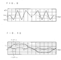
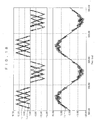
- FIG. 18 is a graph illustrating the values of the currents i u1 , i u2 and i u exhibited when the configuration exhibited in FIG. 12 and the configuration exhibited in FIG. 17 are used.
- FIG. 19 is a graph illustrating the values of the currents i u1 , i u2 and i u exhibited when the configuration exhibited in FIG. 16 and the configuration exhibited in FIG. 17 are used.
- the graph of FIG. 19 shows that the ripple is reduced as compared with the graph of FIG. 18 .
- FIG. 20 is a circuit diagram illustrating a modification of this preferred embodiment, which is a circuit diagram illustrating a configuration for generating the signals T1 and T2 on the basis of the data I d1 , I d2 and V dc .
- the waveform generator 806 and the multiplier 808 are omitted in the current command generating block 82, and a phase shifter 817 is additionally provided.
- the phase shifter 817 shifts by 15 degrees the phase of the current command value I d1 * outputted by the multiplier 807. Then, the phase shifter 817 outputs a current command value I d2 * that is in opposite phase to the current command value I d1 *.
- the signals T1 and T2 are generated in the same way as in the configuration of FIG. 12 when the carrier generator 814 generates the same carrier C as the carrier generator 813 and PWM modulation is performed.
- the carrier generator 814 can be merged with the carrier generator 813 as in FIG. 12 .
- the signals T1 and T2 are generated in the same way as in the configuration of FIG. 16 , and the ripple having the carrier frequency is canceled in the rectified currents i d1 and i d2 .
- a three-phase transformer may be adopted in which primary windings 211, 221, 231 and secondary windings 212, 222, 232 are coupled with each other.
- a three-phase transformer having three primary windings 211, 221 and 231 and three secondary windings 212, 222, 232 coupled with them.
- the secondary windings 212, 222, 232 are all provided with center taps.
- the primary windings 211, 221, 231 are delta-connected, and the three center taps are individually connected to a connection point at which the primary windings 211 and 221 are connected together, a connection point at which the primary windings 221 and 231 are connected together, and a connection point at which the primary windings 231 and 232 are connected together.
- Such a three-phase transformer is illustrated in FIG. 7 of Non-Patent Document 2, for example.
Claims (12)
- Circuit de rectification comprenant :un premier pont de diode triphasé (31) ayant trois extrémités d'entrée (31 U, 31 V, 31 W) et une paire d'extrémités de sortie (31P, 31N), ledit premier pont de diode triphasé appliquant une rectification à onde entière à des courants (iu1, iv1, iw1) entrés auxdites extrémités d'entrée pour obtenir un premier courant rectifié (id1), et délivrer en sortie ledit premier courant rectifié à partir de l'une (31P) desdites extrémités de sortie ;un premier hacheur (41 ; 43) ayant une paire d'extrémités de sortie (41P, 41N ; 43P, 43N), ledit premier hacheur exécutant une première opération de hachage pour recevoir ledit premier courant rectifié en tant qu'un courant dont une fréquence fondamentale a une première valeur ;un second pont de diode triphasé (32) ayant trois extrémités d'entrée (32U, 32V, 32W) et une paire d'extrémités de sortie (32P, 32N), ledit second pont de diode triphasé appliquant une rectification à onde entière à des courants (iu2, iV2, iw2) entrés auxdites extrémités d'entrée pour obtenir un second courant rectifié (id2), et délivrer en sortie ledit second courant rectifié à partir de l'une (32P) desdites extrémités de sortie ; etun second hacheur (42 ; 44) ayant une paire d'extrémités de sortie (42P, 42N ; 44P, 44N), ledit second hacheur exécutant une seconde opération de hachage pour recevoir ledit second courant rectifié en tant qu'un courant dont une fréquence fondamentale a ladite première valeur ;ladite paire d'extrémités de sortie dudit premier hacheur et ladite paire d'extrémités de sortie dudit second hacheur étant connectées en parallèle, caractérisé en ce quedes premiers courants alternatifs triphasés (iu1, iv1, iw1) sont entrés auxdites extrémités d'entrée (31 U, 31 V, 31 W) dudit premier pont de diode triphasé (31) et contrôlés sur la base de la première opération de hachage, une fréquence fondamentale desdits premiers courants alternatifs triphasés est une seconde valeur qui est 1/6e de ladite première valeur et lesdits premiers courants alternatifs triphasés ayant des différences de phase mutuelles de 120 degrés à la fréquence fondamentale, etdes seconds courants alternatifs triphasés (iu2, iv2, iw2) sont entrés auxdites extrémités d'entrée (31 U, 31 V, 31 W) dudit second pont de diode triphasé (32) et contrôlés sur la base de la seconde opération de hachage, une fréquence fondamentale desdits seconds courants alternatifs triphasés est ladite seconde valeur et ayant des différences de phase mutuelles de 120 degrés à la fréquence fondamentale,et dans lequel il y a une différence de phase de 30 degrés à la fréquence fondamentale entre lesdits premiers courants alternatifs triphasés et lesdits seconds courants alternatifs triphasés, et dans lequel lesdits premiers courants alternatifs triphasés et lesdits seconds courants alternatifs triphasés ont chacun une forme d'onde qui est représentée par l'expression (4), Id représentant la valeur de crête des premier et second courants rectifiés :

- Circuit de rectification selon la revendication 1, comprenant en outre un réacteur interphase (71) qui est connecté auxdites extrémités d'entrée dudit premier pont de diode triphasé (31) et dans lequel les courants (iu1, iv1, iw1) entrés auxdites extrémités d'entrée circulent.
- Circuit de rectification selon la revendication 1, comprenant en outre un réacteur interphase (72) qui est connecté entre ledit premier pont de diode triphasé et ledit premier hacheur et dans lequel ledit premier courant rectifié (id1) circule.
- Circuit de rectification selon la revendication 1,
dans lequel ledit premier hacheur (43) comprend :une première bobine d'induction (411) dans laquelle ledit premier courant rectifié (id1) circule ;une première diode (413) ayant une anode connectée à ladite une (31P) desdites extrémités de sortie dudit premier pont de diode triphasé (31) à travers ladite première bobine d'induction, et une cathode connectée à l'une (43P) desdites extrémités de sortie dudit premier hacheur ;une deuxième bobine d'induction (431) connectée à l'autre (31N) desdites extrémités de sortie dudit premier pont de diode triphasé ;une deuxième diode (434) ayant une cathode connectée à ladite autre (31N) desdites extrémités de sortie dudit premier pont de diode triphasé à travers ladite deuxième bobine d'induction, et une anode connectée à l'autre (43N) desdites extrémités de sortie dudit premier hacheur ; etun élément de commutation (412) ayant une première extrémité connectée à l'anode de ladite première diode et une seconde extrémité connectée à l'anode de ladite deuxième diode, ledit élément de commutation s'ouvrant/se fermant entre ladite première extrémité et ladite seconde extrémité,et dans lequel ledit second hacheur (44) comprend :une troisième bobine d'induction (421) dans laquelle ledit second courant rectifié (id2) circule ;une troisième diode (423) ayant une anode connectée à ladite une (32P) desdites extrémités de sortie dudit second pont de diode triphasé (32) à travers ladite troisième bobine d'induction, et une cathode connectée à l'une (44P) desdites extrémités de sortie dudit second hacheur ;une quatrième bobine d'induction (441) connectée à l'autre (32N) desdites extrémités de sortie dudit second pont de diode triphasé ;une quatrième diode (444) ayant une cathode connectée à ladite autre (32N) desdites extrémités de sortie dudit second pont de diode triphasé à travers ladite quatrième bobine d'induction, et une anode connectée à l'autre (44N) desdites extrémités de sortie dudit second hacheur ; etun élément de commutation (422) ayant une première extrémité connectée à l'anode de ladite troisième diode et une seconde extrémité connectée à l'anode de ladite quatrième diode, ledit élément de commutation s'ouvrant/se fermant entre ladite première extrémité et ladite seconde extrémité. - Circuit de rectification selon la revendication 1, dans lequel ledit premier hacheur et ledit second hacheur sont tous les deux des hacheurs élévateurs.
- Circuit de rectification selon la revendication 1, dans lequel ladite première opération de hachage est contrôlée par modulation d'impulsions en durée sur la base d'une première onde de modulation ayant une fréquence porteuse, et ladite seconde opération de hachage est contrôlée par modulation d'impulsions en durée sur la base d'une seconde onde de modulation ayant ladite fréquence porteuse et étant opposée en phase à ladite première onde de modulation.
- Circuit de rectification selon la revendication 1, comprenant en outre un condensateur de lissage (5) connecté en parallèle aux dites extrémités de sortie dudit premier hacheur et auxdites extrémités de sortie dudit second hacheur.
- Circuit de rectification selon la revendication 1, dans lequel la forme d'onde de chacun desdits premiers courants alternatifs triphasés et desdits seconds courants alternatifs triphasés présente une onde triangulaire dans lesdites première à quatrième sections.
- Circuit de rectification selon la revendication 1, dans lequel, dans lesdites première à quatrième sections, la forme d'onde de chacun desdits premiers courants alternatifs triphasés et desdits seconds courants alternatifs triphasés présente une forme d'onde formée par la combinaison d'une courbe qui est similaire à une forme d'onde qu'une onde sinusoïdale présente de 0 degré à 30 degrés et une forme d'onde qui est symétrique à la courbe de gauche à droite.
- Dispositif de rectification triphasé comprenant :le circuit de rectification selon l'une quelconque des revendications 1 à 9 ; etun transformateur triphasé (2) qui reçoit des courants triphasés (iu, iv, iw), une fréquence fondamentale desdits courants triphasés étant une seconde valeur qui est 1/6e de ladite première valeur et lesdits courants triphasés ayant des différences de phase mutuelles de 120 degrés à la fréquence fondamentale, et qui délivre en sortie des premiers courants alternatifs triphasés (iu1, iv1, iw1) ayant des différences de phase de 15 degrés à la fréquence fondamentale respectivement par rapport auxdits courants triphasés, et qui délivre également en sortie des seconds courants alternatifs triphasés (iu2, iV2, iw2) ayant des différences de phase de 30 degrés à la fréquence fondamentale par rapport auxdits courants triphasés.
- Dispositif de rectification triphasé selon la revendication 10, dans lequel ledit transformateur triphasé (2) comprend trois autotransformateurs (21, 22, 23) chacun ayant un enroulement primaire (211, 221, 232) et un enroulement secondaire (212, 222, 232) couplé audit enroulement primaire et ayant une prise centrale,
lesdits enroulements primaires desdits trois autotransformateurs sont connectés en delta, et
ladite prise centrale de chacun desdits autotransformateurs est connectée à un point de connexion (U, V, W) qui connecte une paire desdits enroulements primaires autres que ledit enroulement primaire couplé audit enroulement secondaire auquel ladite prise centrale appartient. - Dispositif de rectification triphasé selon la revendication 10, dans lequel ledit transformateur triphasé (2) comprend :trois enroulements primaires (211, 221, 231) correspondant à des phases respectives ; ettrois enroulements secondaires (212, 222, 232) couplés à la totalité desdits enroulements primaires et chacun ayant une prise centrale, et dans lequel lesdits enroulements primaires sont connectés en delta, et lesdites trois prises centrales sont individuellement connectées à trois points de connexion (U, V, W) auxquels une paire desdits enroulements primaires sont connectés ensemble.
Applications Claiming Priority (2)
| Application Number | Priority Date | Filing Date | Title |
|---|---|---|---|
| JP2006000513A JP4069945B2 (ja) | 2006-01-05 | 2006-01-05 | 整流回路及び三相整流装置 |
| PCT/JP2006/324941 WO2007077717A1 (fr) | 2006-01-05 | 2006-12-14 | Circuit de rectification et circuit de rectification triphase |
Publications (3)
| Publication Number | Publication Date |
|---|---|
| EP1978629A1 EP1978629A1 (fr) | 2008-10-08 |
| EP1978629A4 EP1978629A4 (fr) | 2017-03-01 |
| EP1978629B1 true EP1978629B1 (fr) | 2018-10-03 |
Family
ID=38228075
Family Applications (1)
| Application Number | Title | Priority Date | Filing Date |
|---|---|---|---|
| EP06834695.6A Not-in-force EP1978629B1 (fr) | 2006-01-05 | 2006-12-14 | Circuit de rectification et circuit de rectification triphase |
Country Status (7)
| Country | Link |
|---|---|
| US (1) | US7898829B2 (fr) |
| EP (1) | EP1978629B1 (fr) |
| JP (1) | JP4069945B2 (fr) |
| KR (1) | KR100982124B1 (fr) |
| CN (1) | CN101326705B (fr) |
| AU (1) | AU2006333893B2 (fr) |
| WO (1) | WO2007077717A1 (fr) |
Families Citing this family (36)
| Publication number | Priority date | Publication date | Assignee | Title |
|---|---|---|---|---|
| JP5282424B2 (ja) | 2008-03-14 | 2013-09-04 | ダイキン工業株式会社 | 整流回路 |
| EP2228894A1 (fr) * | 2009-03-10 | 2010-09-15 | ABB Schweiz AG | Redresseur doté d'un circuit convertisseur à plusieurs niveaux |
| KR101042844B1 (ko) * | 2009-04-22 | 2011-06-17 | 서울대학교산학협력단 | 입력 전류 고조파를 저감시키기 위한 3상 정류 시스템 및 방법 |
| JP2012010507A (ja) * | 2010-06-25 | 2012-01-12 | Mitsubishi Electric Corp | 直流電源装置 |
| JP5523297B2 (ja) * | 2010-12-17 | 2014-06-18 | 東芝三菱電機産業システム株式会社 | 電力変換装置 |
| WO2012116263A1 (fr) * | 2011-02-24 | 2012-08-30 | Crane Electronics, Inc. | Système de conversion de puissance alternatif / continu et procédé pour sa fabrication |
| US8576594B2 (en) | 2011-04-04 | 2013-11-05 | Hamilton Sundstrand Corporation | Soft starter for phase-shifting autotransformer AC-DC power converter |
| US8890630B2 (en) | 2011-07-18 | 2014-11-18 | Crane Electronics, Inc. | Oscillator apparatus and method with wide adjustable frequency range |
| US8885308B2 (en) | 2011-07-18 | 2014-11-11 | Crane Electronics, Inc. | Input control apparatus and method with inrush current, under and over voltage handling |
| CN103178729B (zh) * | 2011-12-22 | 2015-07-22 | 儒竞艾默生环境优化技术(上海)有限公司 | 单相可控整流器的控制系统 |
| CN103187890B (zh) * | 2011-12-27 | 2015-05-06 | 上海儒竞电子科技有限公司 | 三相可控整流器的控制系统 |
| CN103187891B (zh) * | 2011-12-28 | 2015-11-18 | 上海儒竞电子科技有限公司 | 单相可控整流器的载波调幅控制系统 |
| JP5765287B2 (ja) * | 2012-04-12 | 2015-08-19 | 三菱電機株式会社 | コンバータ制御装置及びコンバータ制御装置を備えた空気調和機 |
| US8866551B2 (en) | 2012-09-10 | 2014-10-21 | Crane Electronics, Inc. | Impedance compensation for operational amplifiers used in variable environments |
| US9270198B2 (en) * | 2013-03-12 | 2016-02-23 | University Of Tennessee Research Foundation | Control of parallel-connected current source rectifiers |
| RU2529215C1 (ru) * | 2013-04-11 | 2014-09-27 | Федеральное государственное бюджетное образовательное учреждение высшего профессионального образования "Московский государственный технологический университет "СТАНКИН" (ФГБОУ ВПО МГТУ "СТАНКИН") | Двенадцатифазный понижающий автотрансформаторный преобразователь числа фаз |
| US9197138B2 (en) * | 2013-10-03 | 2015-11-24 | Hamilton Sundstrand Corporation | Voltage step-up six-phase autotransformer passive rectification AC-DC converter |
| CN104578873B (zh) * | 2013-10-15 | 2017-07-04 | 北京凯德恒源科技发展有限公司 | 高质量光伏发电并网系统dc/ac变换器控制方法 |
| CN105850025B (zh) * | 2013-12-26 | 2018-02-09 | 三菱电机株式会社 | 电力变换装置 |
| US9787246B2 (en) * | 2014-03-15 | 2017-10-10 | Mitsubishi Electric Corporation | Motor drive control device, compressor, air-sending device, and air-conditioning apparatus |
| US9041378B1 (en) | 2014-07-17 | 2015-05-26 | Crane Electronics, Inc. | Dynamic maneuvering configuration for multiple control modes in a unified servo system |
| US9831768B2 (en) | 2014-07-17 | 2017-11-28 | Crane Electronics, Inc. | Dynamic maneuvering configuration for multiple control modes in a unified servo system |
| US9230726B1 (en) | 2015-02-20 | 2016-01-05 | Crane Electronics, Inc. | Transformer-based power converters with 3D printed microchannel heat sink |
| US9160228B1 (en) | 2015-02-26 | 2015-10-13 | Crane Electronics, Inc. | Integrated tri-state electromagnetic interference filter and line conditioning module |
| CN104836463B (zh) * | 2015-04-30 | 2018-01-05 | 华南理工大学 | 基于三相pwm整流与多单元不控整流的混合变换系统 |
| US9293999B1 (en) | 2015-07-17 | 2016-03-22 | Crane Electronics, Inc. | Automatic enhanced self-driven synchronous rectification for power converters |
| US9780635B1 (en) | 2016-06-10 | 2017-10-03 | Crane Electronics, Inc. | Dynamic sharing average current mode control for active-reset and self-driven synchronous rectification for power converters |
| US9735566B1 (en) | 2016-12-12 | 2017-08-15 | Crane Electronics, Inc. | Proactively operational over-voltage protection circuit |
| US9742183B1 (en) | 2016-12-09 | 2017-08-22 | Crane Electronics, Inc. | Proactively operational over-voltage protection circuit |
| US9979285B1 (en) | 2017-10-17 | 2018-05-22 | Crane Electronics, Inc. | Radiation tolerant, analog latch peak current mode control for power converters |
| US10425080B1 (en) | 2018-11-06 | 2019-09-24 | Crane Electronics, Inc. | Magnetic peak current mode control for radiation tolerant active driven synchronous power converters |
| US10742133B1 (en) | 2019-01-25 | 2020-08-11 | Hamilton Sunstrand Corporation | Power converters, power distribution systems and methods of converting power |
| RU2709454C1 (ru) * | 2019-02-19 | 2019-12-18 | Илья Николаевич Джус | Выпрямитель |
| US11239763B2 (en) * | 2020-01-06 | 2022-02-01 | Hamilton Sundstrand Corporation | Interphase power transformer for electrical systems |
| CN114142748B (zh) * | 2021-11-19 | 2023-07-21 | 广东福德电子有限公司 | 一种大功率直流电源的主电路拓扑与控制方法 |
| CN114465494A (zh) * | 2021-12-14 | 2022-05-10 | 广东福德电子有限公司 | 一种大功率脉冲负载的直流电源及控制方法 |
Family Cites Families (10)
| Publication number | Priority date | Publication date | Assignee | Title |
|---|---|---|---|---|
| JPS5915475B2 (ja) | 1980-03-24 | 1984-04-10 | 久男 松本 | 交流電流波形を改良した3相周波数変換装置 |
| JP2857094B2 (ja) * | 1995-12-28 | 1999-02-10 | 株式会社東芝 | 三相整流装置 |
| JP3129971B2 (ja) * | 1996-08-14 | 2001-01-31 | サンケン電気株式会社 | トランスレス型三相コンバータ装置 |
| JP3801305B2 (ja) * | 1997-05-20 | 2006-07-26 | 株式会社安川電機 | 整流装置 |
| FR2772526B1 (fr) * | 1997-12-17 | 2000-02-11 | Schneider Electric Sa | Convertisseur alternatif-continu triphase |
| US6122183A (en) * | 1998-11-24 | 2000-09-19 | Lucent Technologies Inc. | Two-stage, three-phase boost converter with reduced total harmonic distortion |
| US6950322B2 (en) * | 2003-04-10 | 2005-09-27 | Rsm Electron Power, Inc. | Regulated AC to DC converter for aerospace applications |
| CN2636496Y (zh) * | 2003-07-24 | 2004-08-25 | 中国科学院近代物理研究所 | 大功率四象限直流脉冲开关电源 |
| JP4371774B2 (ja) * | 2003-11-06 | 2009-11-25 | オークマ株式会社 | インバータ制御装置 |
| JP4351916B2 (ja) * | 2004-01-16 | 2009-10-28 | 株式会社東芝 | ノイズフィルタ |
-
2006
- 2006-01-05 JP JP2006000513A patent/JP4069945B2/ja not_active Expired - Fee Related
- 2006-12-14 KR KR1020087015823A patent/KR100982124B1/ko active IP Right Grant
- 2006-12-14 AU AU2006333893A patent/AU2006333893B2/en not_active Ceased
- 2006-12-14 CN CN2006800463774A patent/CN101326705B/zh not_active Expired - Fee Related
- 2006-12-14 WO PCT/JP2006/324941 patent/WO2007077717A1/fr active Application Filing
- 2006-12-14 US US12/087,344 patent/US7898829B2/en not_active Expired - Fee Related
- 2006-12-14 EP EP06834695.6A patent/EP1978629B1/fr not_active Not-in-force
Non-Patent Citations (1)
| Title |
|---|
| None * |
Also Published As
| Publication number | Publication date |
|---|---|
| KR100982124B1 (ko) | 2010-09-14 |
| JP2007185019A (ja) | 2007-07-19 |
| US20090067206A1 (en) | 2009-03-12 |
| AU2006333893A1 (en) | 2007-07-12 |
| CN101326705B (zh) | 2012-05-09 |
| EP1978629A1 (fr) | 2008-10-08 |
| KR20080078702A (ko) | 2008-08-27 |
| US7898829B2 (en) | 2011-03-01 |
| CN101326705A (zh) | 2008-12-17 |
| JP4069945B2 (ja) | 2008-04-02 |
| AU2006333893B2 (en) | 2010-06-24 |
| EP1978629A4 (fr) | 2017-03-01 |
| WO2007077717A1 (fr) | 2007-07-12 |
Similar Documents
| Publication | Publication Date | Title |
|---|---|---|
| EP1978629B1 (fr) | Circuit de rectification et circuit de rectification triphase | |
| JP6497553B2 (ja) | 交流−直流変換装置 | |
| JP5866010B2 (ja) | 電力変換装置 | |
| JP4512117B2 (ja) | 多重電力変換装置、及び多重変圧器 | |
| Kalpana et al. | Autoconnected-transformer-based 20-pulse AC–DC converter for telecommunication power supply | |
| EP2320551B1 (fr) | Transformateur de puissance à trente-six impulsions et convertisseur de puissance l'intégrant | |
| Biela et al. | Closed-loop sinusoidal input-current shaping of 12-pulse autotransformer rectifier unit with impressed output voltage | |
| Badin et al. | Unity power factor isolated three-phase rectifier with two single-phase buck rectifiers based on the Scott transformer | |
| Meng et al. | Active harmonic suppression of paralleled 12-pulse rectifier at DC side | |
| US7679940B2 (en) | Three-phase voltage source inverter system | |
| US20140241019A1 (en) | Multi-level rectifiers | |
| Pool-Mazun et al. | A direct switch-mode three-phase AC to DC rectifier with high-frequency isolation for fast EV battery chargers | |
| JP2004248430A (ja) | 交流−交流電力変換器の制御装置 | |
| US11876438B2 (en) | Reducing input harmonic distortion in a power supply | |
| JPH09135570A (ja) | 多重整流回路 | |
| JP5431826B2 (ja) | Dc/dcコンバータおよび電力変換装置 | |
| JP3399288B2 (ja) | サイリスタ変換装置 | |
| Fukuda et al. | An auxiliary-supply-assisted twelve-pulse diode rectifier with reduced input current harmonics | |
| Ikeda et al. | A Study on Efficiency, Output Voltage Ripple and Harmonics of 24-Pulse Converter with Special Winding Structure Transformer | |
| Enjeti et al. | Autotransformer configurations to enhance utility power quality of high power AC/DC rectifier systems | |
| JP2012010507A (ja) | 直流電源装置 | |
| JP3580089B2 (ja) | ダイオード整流回路 | |
| Wang et al. | Low harmonic 12-pulse rectifier with a circulating current shaping circuit | |
| JP2019146433A (ja) | 電力変換装置 | |
| JP2006042579A (ja) | スイッチング制御方法、整流装置及び駆動システム |
Legal Events
| Date | Code | Title | Description |
|---|---|---|---|
| PUAI | Public reference made under article 153(3) epc to a published international application that has entered the european phase |
Free format text: ORIGINAL CODE: 0009012 |
|
| 17P | Request for examination filed |
Effective date: 20080702 |
|
| AK | Designated contracting states |
Kind code of ref document: A1 Designated state(s): AT BE BG CH CY CZ DE DK EE ES FI FR GB GR HU IE IS IT LI LT LU LV MC NL PL PT RO SE SI SK TR |
|
| DAX | Request for extension of the european patent (deleted) | ||
| RA4 | Supplementary search report drawn up and despatched (corrected) |
Effective date: 20170201 |
|
| RIC1 | Information provided on ipc code assigned before grant |
Ipc: H02M 7/12 20060101AFI20170126BHEP Ipc: H02M 3/155 20060101ALI20170126BHEP Ipc: H02M 7/08 20060101ALI20170126BHEP |
|
| 17Q | First examination report despatched |
Effective date: 20171120 |
|
| REG | Reference to a national code |
Ref country code: DE Ref legal event code: R079 Ref document number: 602006056510 Country of ref document: DE Free format text: PREVIOUS MAIN CLASS: H02M0007120000 Ipc: H02M0001420000 |
|
| GRAP | Despatch of communication of intention to grant a patent |
Free format text: ORIGINAL CODE: EPIDOSNIGR1 |
|
| RIC1 | Information provided on ipc code assigned before grant |
Ipc: H02M 7/12 20060101ALI20180516BHEP Ipc: H02M 7/08 20060101ALI20180516BHEP Ipc: H02M 3/156 20060101ALI20180516BHEP Ipc: H02M 1/42 20070101AFI20180516BHEP Ipc: H02M 5/14 20060101ALI20180516BHEP |
|
| INTG | Intention to grant announced |
Effective date: 20180613 |
|
| GRAS | Grant fee paid |
Free format text: ORIGINAL CODE: EPIDOSNIGR3 |
|
| GRAA | (expected) grant |
Free format text: ORIGINAL CODE: 0009210 |
|
| AK | Designated contracting states |
Kind code of ref document: B1 Designated state(s): AT BE BG CH CY CZ DE DK EE ES FI FR GB GR HU IE IS IT LI LT LU LV MC NL PL PT RO SE SI SK TR |
|
| REG | Reference to a national code |
Ref country code: GB Ref legal event code: FG4D |
|
| REG | Reference to a national code |
Ref country code: CH Ref legal event code: EP Ref country code: AT Ref legal event code: REF Ref document number: 1049697 Country of ref document: AT Kind code of ref document: T Effective date: 20181015 |
|
| REG | Reference to a national code |
Ref country code: IE Ref legal event code: FG4D Ref country code: DE Ref legal event code: R096 Ref document number: 602006056510 Country of ref document: DE |
|
| REG | Reference to a national code |
Ref country code: NL Ref legal event code: MP Effective date: 20181003 |
|
| REG | Reference to a national code |
Ref country code: LT Ref legal event code: MG4D |
|
| REG | Reference to a national code |
Ref country code: AT Ref legal event code: MK05 Ref document number: 1049697 Country of ref document: AT Kind code of ref document: T Effective date: 20181003 |
|
| PG25 | Lapsed in a contracting state [announced via postgrant information from national office to epo] |
Ref country code: NL Free format text: LAPSE BECAUSE OF FAILURE TO SUBMIT A TRANSLATION OF THE DESCRIPTION OR TO PAY THE FEE WITHIN THE PRESCRIBED TIME-LIMIT Effective date: 20181003 |
|
| PG25 | Lapsed in a contracting state [announced via postgrant information from national office to epo] |
Ref country code: ES Free format text: LAPSE BECAUSE OF FAILURE TO SUBMIT A TRANSLATION OF THE DESCRIPTION OR TO PAY THE FEE WITHIN THE PRESCRIBED TIME-LIMIT Effective date: 20181003 Ref country code: LT Free format text: LAPSE BECAUSE OF FAILURE TO SUBMIT A TRANSLATION OF THE DESCRIPTION OR TO PAY THE FEE WITHIN THE PRESCRIBED TIME-LIMIT Effective date: 20181003 Ref country code: IS Free format text: LAPSE BECAUSE OF FAILURE TO SUBMIT A TRANSLATION OF THE DESCRIPTION OR TO PAY THE FEE WITHIN THE PRESCRIBED TIME-LIMIT Effective date: 20190203 Ref country code: CZ Free format text: LAPSE BECAUSE OF FAILURE TO SUBMIT A TRANSLATION OF THE DESCRIPTION OR TO PAY THE FEE WITHIN THE PRESCRIBED TIME-LIMIT Effective date: 20181003 Ref country code: BG Free format text: LAPSE BECAUSE OF FAILURE TO SUBMIT A TRANSLATION OF THE DESCRIPTION OR TO PAY THE FEE WITHIN THE PRESCRIBED TIME-LIMIT Effective date: 20190103 Ref country code: PL Free format text: LAPSE BECAUSE OF FAILURE TO SUBMIT A TRANSLATION OF THE DESCRIPTION OR TO PAY THE FEE WITHIN THE PRESCRIBED TIME-LIMIT Effective date: 20181003 Ref country code: AT Free format text: LAPSE BECAUSE OF FAILURE TO SUBMIT A TRANSLATION OF THE DESCRIPTION OR TO PAY THE FEE WITHIN THE PRESCRIBED TIME-LIMIT Effective date: 20181003 Ref country code: FI Free format text: LAPSE BECAUSE OF FAILURE TO SUBMIT A TRANSLATION OF THE DESCRIPTION OR TO PAY THE FEE WITHIN THE PRESCRIBED TIME-LIMIT Effective date: 20181003 Ref country code: LV Free format text: LAPSE BECAUSE OF FAILURE TO SUBMIT A TRANSLATION OF THE DESCRIPTION OR TO PAY THE FEE WITHIN THE PRESCRIBED TIME-LIMIT Effective date: 20181003 |
|
| PG25 | Lapsed in a contracting state [announced via postgrant information from national office to epo] |
Ref country code: SE Free format text: LAPSE BECAUSE OF FAILURE TO SUBMIT A TRANSLATION OF THE DESCRIPTION OR TO PAY THE FEE WITHIN THE PRESCRIBED TIME-LIMIT Effective date: 20181003 Ref country code: GR Free format text: LAPSE BECAUSE OF FAILURE TO SUBMIT A TRANSLATION OF THE DESCRIPTION OR TO PAY THE FEE WITHIN THE PRESCRIBED TIME-LIMIT Effective date: 20190104 Ref country code: PT Free format text: LAPSE BECAUSE OF FAILURE TO SUBMIT A TRANSLATION OF THE DESCRIPTION OR TO PAY THE FEE WITHIN THE PRESCRIBED TIME-LIMIT Effective date: 20190203 |
|
| REG | Reference to a national code |
Ref country code: DE Ref legal event code: R119 Ref document number: 602006056510 Country of ref document: DE |
|
| PG25 | Lapsed in a contracting state [announced via postgrant information from national office to epo] |
Ref country code: IT Free format text: LAPSE BECAUSE OF FAILURE TO SUBMIT A TRANSLATION OF THE DESCRIPTION OR TO PAY THE FEE WITHIN THE PRESCRIBED TIME-LIMIT Effective date: 20181003 Ref country code: DK Free format text: LAPSE BECAUSE OF FAILURE TO SUBMIT A TRANSLATION OF THE DESCRIPTION OR TO PAY THE FEE WITHIN THE PRESCRIBED TIME-LIMIT Effective date: 20181003 |
|
| REG | Reference to a national code |
Ref country code: CH Ref legal event code: PL |
|
| PLBE | No opposition filed within time limit |
Free format text: ORIGINAL CODE: 0009261 |
|
| STAA | Information on the status of an ep patent application or granted ep patent |
Free format text: STATUS: NO OPPOSITION FILED WITHIN TIME LIMIT |
|
| PG25 | Lapsed in a contracting state [announced via postgrant information from national office to epo] |
Ref country code: EE Free format text: LAPSE BECAUSE OF FAILURE TO SUBMIT A TRANSLATION OF THE DESCRIPTION OR TO PAY THE FEE WITHIN THE PRESCRIBED TIME-LIMIT Effective date: 20181003 Ref country code: RO Free format text: LAPSE BECAUSE OF FAILURE TO SUBMIT A TRANSLATION OF THE DESCRIPTION OR TO PAY THE FEE WITHIN THE PRESCRIBED TIME-LIMIT Effective date: 20181003 Ref country code: MC Free format text: LAPSE BECAUSE OF FAILURE TO SUBMIT A TRANSLATION OF THE DESCRIPTION OR TO PAY THE FEE WITHIN THE PRESCRIBED TIME-LIMIT Effective date: 20181003 Ref country code: SK Free format text: LAPSE BECAUSE OF FAILURE TO SUBMIT A TRANSLATION OF THE DESCRIPTION OR TO PAY THE FEE WITHIN THE PRESCRIBED TIME-LIMIT Effective date: 20181003 Ref country code: LU Free format text: LAPSE BECAUSE OF NON-PAYMENT OF DUE FEES Effective date: 20181214 |
|
| 26N | No opposition filed |
Effective date: 20190704 |
|
| REG | Reference to a national code |
Ref country code: IE Ref legal event code: MM4A |
|
| GBPC | Gb: european patent ceased through non-payment of renewal fee |
Effective date: 20190103 |
|
| REG | Reference to a national code |
Ref country code: BE Ref legal event code: MM Effective date: 20181231 |
|
| PG25 | Lapsed in a contracting state [announced via postgrant information from national office to epo] |
Ref country code: IE Free format text: LAPSE BECAUSE OF NON-PAYMENT OF DUE FEES Effective date: 20181214 Ref country code: FR Free format text: LAPSE BECAUSE OF NON-PAYMENT OF DUE FEES Effective date: 20181231 Ref country code: DE Free format text: LAPSE BECAUSE OF NON-PAYMENT OF DUE FEES Effective date: 20190702 Ref country code: SI Free format text: LAPSE BECAUSE OF FAILURE TO SUBMIT A TRANSLATION OF THE DESCRIPTION OR TO PAY THE FEE WITHIN THE PRESCRIBED TIME-LIMIT Effective date: 20181003 |
|
| PG25 | Lapsed in a contracting state [announced via postgrant information from national office to epo] |
Ref country code: BE Free format text: LAPSE BECAUSE OF NON-PAYMENT OF DUE FEES Effective date: 20181231 |
|
| PG25 | Lapsed in a contracting state [announced via postgrant information from national office to epo] |
Ref country code: LI Free format text: LAPSE BECAUSE OF NON-PAYMENT OF DUE FEES Effective date: 20181231 Ref country code: CH Free format text: LAPSE BECAUSE OF NON-PAYMENT OF DUE FEES Effective date: 20181231 Ref country code: GB Free format text: LAPSE BECAUSE OF NON-PAYMENT OF DUE FEES Effective date: 20190103 |
|
| PG25 | Lapsed in a contracting state [announced via postgrant information from national office to epo] |
Ref country code: TR Free format text: LAPSE BECAUSE OF FAILURE TO SUBMIT A TRANSLATION OF THE DESCRIPTION OR TO PAY THE FEE WITHIN THE PRESCRIBED TIME-LIMIT Effective date: 20181003 |
|
| PG25 | Lapsed in a contracting state [announced via postgrant information from national office to epo] |
Ref country code: HU Free format text: LAPSE BECAUSE OF FAILURE TO SUBMIT A TRANSLATION OF THE DESCRIPTION OR TO PAY THE FEE WITHIN THE PRESCRIBED TIME-LIMIT; INVALID AB INITIO Effective date: 20061214 Ref country code: CY Free format text: LAPSE BECAUSE OF FAILURE TO SUBMIT A TRANSLATION OF THE DESCRIPTION OR TO PAY THE FEE WITHIN THE PRESCRIBED TIME-LIMIT Effective date: 20181003 |