US9831768B2 - Dynamic maneuvering configuration for multiple control modes in a unified servo system - Google Patents
Dynamic maneuvering configuration for multiple control modes in a unified servo system Download PDFInfo
- Publication number
- US9831768B2 US9831768B2 US14/787,565 US201514787565A US9831768B2 US 9831768 B2 US9831768 B2 US 9831768B2 US 201514787565 A US201514787565 A US 201514787565A US 9831768 B2 US9831768 B2 US 9831768B2
- Authority
- US
- United States
- Prior art keywords
- control
- sub
- voltage
- output
- node
- Prior art date
- Legal status (The legal status is an assumption and is not a legal conclusion. Google has not performed a legal analysis and makes no representation as to the accuracy of the status listed.)
- Active
Links
Images


Classifications
-
- H—ELECTRICITY
- H02—GENERATION; CONVERSION OR DISTRIBUTION OF ELECTRIC POWER
- H02M—APPARATUS FOR CONVERSION BETWEEN AC AND AC, BETWEEN AC AND DC, OR BETWEEN DC AND DC, AND FOR USE WITH MAINS OR SIMILAR POWER SUPPLY SYSTEMS; CONVERSION OF DC OR AC INPUT POWER INTO SURGE OUTPUT POWER; CONTROL OR REGULATION THEREOF
- H02M3/00—Conversion of dc power input into dc power output
- H02M3/02—Conversion of dc power input into dc power output without intermediate conversion into ac
- H02M3/04—Conversion of dc power input into dc power output without intermediate conversion into ac by static converters
- H02M3/10—Conversion of dc power input into dc power output without intermediate conversion into ac by static converters using discharge tubes with control electrode or semiconductor devices with control electrode
- H02M3/145—Conversion of dc power input into dc power output without intermediate conversion into ac by static converters using discharge tubes with control electrode or semiconductor devices with control electrode using devices of a triode or transistor type requiring continuous application of a control signal
- H02M3/155—Conversion of dc power input into dc power output without intermediate conversion into ac by static converters using discharge tubes with control electrode or semiconductor devices with control electrode using devices of a triode or transistor type requiring continuous application of a control signal using semiconductor devices only
- H02M3/156—Conversion of dc power input into dc power output without intermediate conversion into ac by static converters using discharge tubes with control electrode or semiconductor devices with control electrode using devices of a triode or transistor type requiring continuous application of a control signal using semiconductor devices only with automatic control of output voltage or current, e.g. switching regulators
- H02M3/158—Conversion of dc power input into dc power output without intermediate conversion into ac by static converters using discharge tubes with control electrode or semiconductor devices with control electrode using devices of a triode or transistor type requiring continuous application of a control signal using semiconductor devices only with automatic control of output voltage or current, e.g. switching regulators including plural semiconductor devices as final control devices for a single load
- H02M3/1588—Conversion of dc power input into dc power output without intermediate conversion into ac by static converters using discharge tubes with control electrode or semiconductor devices with control electrode using devices of a triode or transistor type requiring continuous application of a control signal using semiconductor devices only with automatic control of output voltage or current, e.g. switching regulators including plural semiconductor devices as final control devices for a single load comprising at least one synchronous rectifier element
-
- H—ELECTRICITY
- H02—GENERATION; CONVERSION OR DISTRIBUTION OF ELECTRIC POWER
- H02M—APPARATUS FOR CONVERSION BETWEEN AC AND AC, BETWEEN AC AND DC, OR BETWEEN DC AND DC, AND FOR USE WITH MAINS OR SIMILAR POWER SUPPLY SYSTEMS; CONVERSION OF DC OR AC INPUT POWER INTO SURGE OUTPUT POWER; CONTROL OR REGULATION THEREOF
- H02M1/00—Details of apparatus for conversion
- H02M1/0003—Details of control, feedback or regulation circuits
- H02M1/0025—Arrangements for modifying reference values, feedback values or error values in the control loop of a converter
-
- H02M2001/0025—
Definitions
- the present disclosure relates to control systems for power electronics devices.
- power supply/converter applications require the power supply to operate within a well-defined operating area bounded by various electrical limits (e.g., voltage, current, power, resistance and conductance).
- the operation of power supplies may be controlled to operate within an operating area to either protect the power supply, protect a load coupled to the power supply, or for some desired control effect.
- the power supply may, for example, be required to provide a constant power output that does not exceed a specified current limit.
- some power supply applications require the power supply to be capable of effectively switching between operating modes. For example, some power supplies may switch between providing a constant voltage to providing a constant current.
- FIG. 1 shows a simplified schematic diagram of a DC/DC power converter 10 .
- the power converter 10 operates by repeatedly opening and closing a power switch 12 .
- the switch 12 may, for example, be a metal oxide semiconductor field-effect transistor (MOSFET).
- MOSFET metal oxide semiconductor field-effect transistor
- closing the switch 12 causes a current to flow from a direct current (DC) input source 14 through a winding of a magnetizable part 16 (e.g., a primary winding of a transformer, an inductor).
- a rough DC voltage is present between terminals of the switch 12 .
- an alternating current (AC) line voltage may, for example, be rectified by a bridge rectifier (not shown) and an associated smoothing capacitor (not shown) to provide rectified and smoothed rough DC voltage to the terminals of the switch.
- AC alternating current
- the switch 12 When the switch 12 is closed, the current that flows through the magnetizable part 16 may cause energy to be stored in the magnetizable part.
- the switch 12 is then opened.
- energy stored in the magnetizable part 16 is transferred to an output node 18 of the power converter through a rectifier and output filter 20 (e.g., a diode and a capacitor).
- the current may charge the output filter 20 .
- the switch 12 In steady state operation in a constant voltage (CV) mode, the switch 12 may be switched to open and close rapidly and in such a manner that the output voltage V OUT on the output filter 20 at the output node 18 remains substantially constant.
- CV constant voltage
- the power converter 10 includes a controller 22 that controls the opening and closing of the switch 12 .
- the controller 22 may take the form of a pulse width modulation (PWM) controller.
- PWM pulse width modulation
- the power converter 10 operates in two control modes that utilize servo feedback control: constant voltage (CV) mode and constant current (CC) mode.
- CV constant voltage
- CC constant current
- the output voltage V OUT is sensed by a voltage sense circuit 24 (e.g., a resistor divider).
- An output node 26 of the voltage sense circuit 24 is coupled to an inverting input terminal of a voltage control amplifier 28 .
- the voltage control amplifier 28 may be coupled to a positive power supply and a negative power supply (e.g., V CC and ground, +V CC and ⁇ V CC , etc.).
- the voltage control amplifier 28 compares the voltage at the output node 26 of the voltage sense circuit to a reference voltage V REF1 coupled to a non-inverting input terminal and outputs the result of the comparison onto an output terminal of the voltage control amplifier 28 at node 29 (V EA ).
- a feedback compensation circuit 30 is coupled between the inverting input terminal of the voltage control amplifier 28 and the output terminal.
- the feedback compensation circuit 30 includes a compensation or feedback capacitor 32 and a feedback resistor 34 connected together in series. If the comparison of the voltage control amplifier 28 inverting input is lower than its non-inverting input (i.e., V OUT is below regulation), then the output voltage of the amplifier 28 will increase to the required voltage at the common control node 38 to maintain regulation of V OUT . If the comparison of the amplifier 28 inverting input is greater than its non-inverting input (i.e., V OUT is above regulation), then the output voltage of the amplifier 28 will decrease to the required voltage at the common control node 38 to maintain regulation of V OUT .
- this error voltage (V CONTROL ) at the common control node 38 is indicative of the output voltage V out at the output node 18 .
- the pull-up resistor 36 provides the sourcing current for the amplifier 28 .
- An input of the controller 22 is coupled to the common control node 38 and, based on the received error voltage, the controller controls the on/off duty cycle of the switch 12 to regulate output voltage V OUT .
- the current I OUT being supplied by the power converter 10 is sensed by a current sense circuit 42 (e.g., a sense resistor).
- the voltage on an output node 44 of the current sense circuit 42 is sensed by a current control amplifier 46 .
- the current control amplifier 46 may be coupled to a positive power supply and a negative power supply (e.g., V CC and ground, +V CC and ⁇ V CC , etc.).
- a feedback compensation circuit 48 is coupled between the inverting input terminal of the voltage control amplifier 46 and the output terminal at node 47 (V CA ).
- the feedback compensation circuit 48 includes a compensation or feedback capacitor 50 and a feedback resistor 52 connected together in series.
- the current control amplifier 46 causes the voltage on an output terminal thereof to decrease to a relatively low voltage as necessary at the common control node 38 (V CONTROL ) to maintain the predetermined limit of the output load I OUT .
- the pull-up resistor 36 provides the sourcing current for the amplifier 46 .
- the voltage sensed by the controller 22 is therefore indicative of the magnitude of the output current I OUT .
- the controller controls the on/off duty cycle of switch 12 to regulate output current I OUT .
- the blocking diodes 40 and 54 are configured such that a minimum error signal is selected and provided to the controller 22 .
- the diodes may be referred to as being in an “ORed” or “ORing” configuration.
- the power converter 10 operates either in the CV mode or in the CC mode, depending on the loading condition. In one example, if the output current exceeds a specified current (e.g., a short circuit or other overcurrent condition), then the power converter 10 operates in the constant current mode. Otherwise, the power converter 10 operates in the constant voltage mode.
- the CC mode acts as a current limiter to protect one or more components of the power converter, such as the switch.
- This “swing” is delayed by several factors.
- One relatively minor factor is the intrinsic delay of the operational amplifier working at its limit (e.g., close to the +V CC rail).
- Another relatively minor factor is the effective slew rate of the operational amplifier.
- a relatively major factor is the time necessary to charge or discharge the local feedback capacitors 32 and 50 to the new output voltage of the respective amplifiers 28 and 46 after control is switched between modes. In some examples, discharging the feedback capacitors 32 and 50 can take several clock cycles (e.g., 50 clock cycles or more at a 550 kHz switching frequency), causing a significant delay in the handoff between control modes, resulting in an extended period of uncontrolled energy applied to one or more components, such as the switch 12 . This delay can cause high transient input current and voltages (e.g., drain voltage) that can potentially damage the switch 12 or other components of the power converter 10 .
- a control circuit to control the operation of a power electronics device may be summarized as including a common control node; a first sub-control circuit that includes: a first amplifier that includes a first input, a second input, and an output; a first capacitive feedback circuit that includes an input coupled to the common control node and an output coupled to the first input of the first amplifier; and a first switch that includes a first terminal and a second terminal, the first terminal coupled to the output of the first amplifier and the second terminal coupled to the common control node; and a second sub-control circuit that includes: a second amplifier that includes a first input, a second input, and an output; a second capacitive feedback circuit that includes an input coupled to the common control node and an output coupled to the first input of the second amplifier; and a second switch that includes a first terminal and a second terminal, the first terminal coupled to the output of the second amplifier and the second terminal coupled to the common control node.
- the control circuit may further include a first reference voltage supply coupled to the second input of the first amplifier; and a second reference voltage supply coupled to the second input of the second amplifier.
- the first reference voltage supply may provide a voltage indicative of a reference output voltage for the power electronics device
- the second reference voltage supply may provide a voltage indicative of a reference output current for the power electronics device.
- the control circuit may further include a controller that includes a control input, the control input electrically coupled to the common control node.
- the control circuit may a voltage sense circuit that includes an output indicative of an output voltage of the power electronics device, the output coupled to the first input of the first amplifier; and a current sense circuit that includes an output indicative of an output current of the power electronics device, the output coupled to the first input of the second amplifier.
- the first switch may be in the form of a first diode and the second switch may be in the form of a second diode.
- the first terminal of the first switch may include a cathode of the first diode and the second terminal of the first switch may include an anode of the first diode, and the first terminal of the second switch may include a cathode of the second diode and the second terminal of the second switch may include an anode of the second diode.
- the control circuit may further include a third sub-control circuit that includes: a third amplifier that includes a first input, a second input, and an output; a third capacitive feedback circuit that includes an input coupled to the common control node and an output coupled to the first input of the third amplifier; and a third switch that includes a first terminal and a second terminal, the first terminal coupled to the output of the third amplifier and the second terminal coupled to the common control node.
- a third sub-control circuit that includes: a third amplifier that includes a first input, a second input, and an output; a third capacitive feedback circuit that includes an input coupled to the common control node and an output coupled to the first input of the third amplifier; and a third switch that includes a first terminal and a second terminal, the first terminal coupled to the output of the third amplifier and the second terminal coupled to the common control node.
- a control circuit to control the operation of a power electronics device may be summarized as including a common control node; a first sub-control circuit that includes: a first forward control portion that includes a first forward control portion input and a first forward control portion output; a first feedback portion that includes a first feedback portion input coupled to the common control node and a first feedback portion output coupled to the first forward control portion input, the first feedback portion stores an electrical charge; and a first switch that includes a first terminal and a second terminal, the first terminal coupled to the first forward portion output and the second terminal coupled to the common control node; and a second sub-control circuit that includes: a second forward control portion that includes a second forward control portion input and a second forward control portion output; a second feedback portion that includes a second feedback portion input coupled to the common control node and a second feedback portion output coupled to the second forward control portion input, the second feedback portion stores an electrical charge; and a second switch that includes a first terminal and a second terminal, the first terminal coupled to the second forward portion output and the second
- the first terminal of the first switch may include a cathode of the first diode and the second terminal of the first switch may include an anode of the first diode
- the first terminal of the second switch may include a cathode of the second diode and the second terminal of the second switch may include an anode of the second diode.
- At least one of the first switch or the second switch may include a transistor.
- the control circuit may further include a third sub-control circuit that includes: a third forward control portion that includes a third forward control portion input and a third forward control portion output; a third feedback portion that includes a third feedback portion input coupled to the common control node and a third feedback portion output coupled to the third forward control portion input, the third feedback portion stores an electrical charge; and a third switch that includes a first terminal and a second terminal, the first terminal coupled to the third forward portion output and the second terminal coupled to the common control node.
- the first forward control portion may include a first amplifier and the second forward control portion may include a second amplifier.
- the control circuit may further include a voltage sense circuit that includes an output indicative of an output voltage of the power electronics device, the output coupled to the first forward control portion input; and a current sense circuit that includes an output indicative of an output current of the power electronics device, the output coupled to the second forward control portion input.
- the power electronics device may include a power converter, and the common control node may be electrically coupled to an input of a controller for the power converter.
- a control circuit to control the operation of a power electronics device may be summarized as including a common control node; a plurality of sub-control circuits, each of the plurality of sub-control circuits includes an output selectively coupled to the common control node via a respective one of a plurality of switches, one of plurality of switches closes at a time, and each of the sub-control circuits include a capacitive feedback circuit having a feedback input electrically coupled to the common control node.
- the control circuit may further include a first reference voltage supply coupled to an input of a first one of the plurality of sub-control circuits; and a second reference voltage supply coupled to an input of a second one of the plurality of sub-control circuits.
- the first reference voltage supply may provide a voltage indicative of a reference output voltage for the power electronics device
- the second reference voltage supply may provide a voltage indicative of a reference output current for the power electronics device.
- the control circuit may further include a controller that includes a control input, the control input electrically coupled to the common control node.
- the control circuit may further include a first parameter sense circuit that includes an output indicative of a first parameter of the power electronics device, the output coupled to an input of a first one of the plurality of sub-control circuits; and a second parameter sense circuit that includes an output indicative of a second parameter of the power electronics device, the output coupled to an input of a second one of the plurality of sub-control circuits.
- At least one of the first parameter or the second parameter may include an output voltage, an output current, or a temperature of a component of the power electronics device.
- At least one of the plurality of switches may be in the form of a diode or a transistor.
- a method of controlling a power electronics device may be summarized as including providing a common control node; coupling the common control node to a controller of the power electronics device; and for each of a plurality of sub-control circuits, coupling an output of the sub-control circuit to the common control node via a switch; and coupling a feedback input of a capacitive feedback circuit to the common control node.
- the method may further include providing a first control signal from a first one of the sub-control circuits to the controller via the common control node by closing a first one of the switches associated with the first one of the sub-control circuits; opening the first one of the switches associated with the first one of the sub-control circuits; and closing a second one of the switches associated with a second one of the plurality of sub-control circuits to provide a second control signal from the second one of the plurality of sub-control circuits to the controller via the common control node.
- FIG. 1 is a block diagram of a conventional power converter.
- FIG. 2 is a block diagram of a power converter that includes two control inputs that dynamically control a servo system, and control circuitry to accelerate handoff between the two control inputs, according to at least one illustrated embodiment.
- FIG. 3A is a graph of an output voltage (V CA ) for a current control amplifier of the conventional power converter of FIG. 1 , an output voltage (V EA ) for a voltage control amplifier of the conventional power converter, and a common control node voltage (V CONTROL ) of the power converter during a transition from a constant voltage control mode to a constant current control mode.
- V CA output voltage
- V EA output voltage
- V CONTROL common control node voltage
- FIG. 3B is a graph of an output voltage (V CA ) for a current control amplifier of the power converter of FIG. 2 , an output voltage (V EA ) for a voltage control amplifier of the power converter, and a common control node voltage (V CONTROL ) of the power converter during a transition from a constant voltage control mode to a constant current control mode.
- V CA output voltage
- V EA output voltage
- V CONTROL common control node voltage
- FIG. 4 is a block diagram of a control circuit that controls the operation of a power electronics device, according to at least one illustrated embodiment.
- FIG. 5 is a flow diagram showing a method for controlling a power electronics device, according to at least one illustrated embodiment.
- Embodiments of the present disclosure are directed to systems and methods for facilitating accelerated handover time between servo control modes for power electronics devices, such as DC/DC power converters, AC/DC power converters, etc.
- One or more embodiments disclosed herein reduce or eliminate high transient input current that would otherwise occur during overcurrent conditions, such as short circuit conditions.
- One or more embodiments may also reduce or eliminate excessive input current ripple and output voltage ripple during startup of a power converter, especially when providing power to a capacitive load, which tends to otherwise cause overshoot or “ringing” at startup.
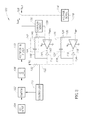
- FIG. 2 shows a power converter 100 that exhibits significantly improved behavior by minimizing transients appearing at the input and output when control of the power converter changes from one control mode to another.
- the power converter 100 operates by repeatedly opening and closing a power switch 102 .
- the switch 102 may, for example, take the form of a metal oxide semiconductor field-effect transistor (MOSFET), a bipolar junction transistor (BJT), one or more diodes, etc.
- the power converter 100 may include a plurality of switches 102 (e.g., two switches used in a push-pull converter).
- the power converter 100 may take the form of a boost converter, buck converter, buck-boost converter, flyback converter, or any other DC/DC, AC/DC, DC/AC, or AC/AC circuits.
- closing the switch 102 causes a current to flow from a direct current (DC) input source 104 through a winding of a magnetizable part 106 , such as a primary winding of transformer or through an inductor.
- a rough DC voltage is present between two terminals of the switch 102 .
- an alternating current (AC) line voltage may, for example, be rectified by a bridge rectifier (not shown) and an associated smoothing capacitor (not shown) to provide rectified and smoothed rough DC voltage to the terminals of the switch 102 .
- the switch 102 When the switch 102 is closed, the current that flows through the magnetizable part 106 causes energy to be stored in the magnetizable part. The switch 102 is then opened. When the switch 102 is opened, energy stored in magnetizable part 106 is transferred to an output node 108 of the power converter 100 in the form of current that flows through a rectifier and output filter 110 (e.g., a diode and a capacitor). The current may charge the output filter 110 . In steady state operation in a constant voltage (CV) mode, the switch 102 may be switched to open and close rapidly and in such a manner that an output voltage V OUT on the output filter 110 at the output node 108 remains substantially constant.
- CV constant voltage
- the power converter 100 includes a controller 112 that controls the opening and closing of the switch 102 .
- the controller 112 may be coupled to a switch driver (not shown).
- the controller 112 is a pulse width modulation (PWM) controller, for example.
- PWM is a modulation technique that controls the width of a control pulse based on modulator signal information.
- the average value of voltage (and current) fed to a load at the output node 108 is controlled by turning the switch 102 between the DC input source 104 and a load (i.e., the circuit or device that receives the power from the power converter) ON and OFF at a fast pace.
- a load i.e., the circuit or device that receives the power from the power converter
- the switching frequency is generally much faster than what would affect the load. Typical switching frequencies for power converters range from the tens to hundreds of kilohertz (kHz), for example 50-600 kHz.
- PWM control power loss in the switching devices is very low. When a switch is OFF there is practically no current, and when it is ON, there is almost no voltage drop across the switch. Power loss, being the product of voltage and current, is thus in both cases close to zero.
- the output voltage V OUT is sensed by a voltage sense circuit 114 (e.g., a resistor divider).
- An output node 116 of the voltage sense circuit 114 is coupled to an inverting input terminal of a voltage control amplifier 118 .
- the voltage control amplifier 118 may be coupled to a positive power supply and a negative power supply (e.g., V CC and ground, +V CC and ⁇ V CC , etc.).
- the voltage control amplifier 118 compares the voltage at the output node 116 of the voltage sense circuit 114 to a reference voltage V REF1 coupled to a non-inverting input terminal and outputs the result of the comparison onto an output terminal of the voltage control amplifier 118 at a node 119 (V EA ).
- a feedback compensation circuit 120 is coupled between the inverting input terminal of the voltage control amplifier and a common control node 122 .
- the feedback compensation circuit 120 includes a compensation or feedback capacitor 124 and a feedback resistor 126 connected together in series.
- An input node 128 of the feedback compensation circuit 120 is coupled to the common control node 122 of the power converter 100 and an output node 130 of the feedback compensation circuit is coupled to the inverting input terminal of the voltage control amplifier 118 .
- different resistor-capacitor (RC) feedback compensation circuits may be utilized to achieve a desired feedback transfer function.
- V CONTROL this error voltage at the common control node 122 is indicative of the output voltage V OUT .
- Pull-up resistor 132 provides the sourcing current for the amplifier 118 .
- a control input of the controller 112 is coupled to the common control node 122 and, based on the received error voltage, the controller 112 controls the on/off duty cycle of the switch 102 to regulate the output voltage V OUT at the output node 108 .
- the current I OUT being supplied by the power converter 100 is sensed by a current sense circuit 136 (e.g., a sense resistor).
- the voltage on an output node 138 of the current sense circuit 136 is coupled to an inverting input terminal of a current control amplifier 140 .
- the current control amplifier 140 may be coupled to a positive power supply and a negative power supply (e.g., V CC and ground, +V CC and ⁇ V CC , etc.).
- the current control amplifier 140 compares the voltage at the output node 138 of the current sense circuit 136 to a reference voltage V REF2 coupled to a non-inverting input terminal and outputs the result of the comparison onto an output terminal of the current control amplifier at a node 141 (V CA ).
- a feedback compensation circuit 142 is coupled between the inverting input terminal of the current control amplifier and the common control node 122 .
- the feedback compensation circuit 142 includes a compensation or feedback capacitor 144 and a feedback resistor 146 connected together in series.
- An input node 148 of the feedback compensation circuit 142 is coupled to the common output node 122 of the power converter 100 and an output node 150 of the feedback compensation circuit is coupled to the inverting input terminal of the current control amplifier 140 .
- different RC feedback compensation circuits may be utilized to achieve a desired feedback transfer function.
- the current control amplifier 140 causes the voltage on an output terminal thereof to decrease to a relatively low voltage as necessary at the common control node 122 (V CONTROL ) to maintain the predetermined limit of the output load I OUT .
- Pull-up resistor 132 provides the sourcing current for the amplifier 140 .
- the voltage sensed by the controller 112 is therefore indicative of the magnitude of the output current I OUT .
- the controller 112 controls the on/off duty cycle of switch to regulate output current I OUT .
- the blocking diodes 134 and 152 are configured as switches such that a minimum error signal is selected and provided to the controller 112 .
- the diodes may be referred to as being in an “ORed” or “ORing” configuration.
- Other passive or active components may be used to achieve the same switching functionality.
- one or more transistors e.g., FETs, BJTs, etc.
- integrated circuits e.g., ideal diode circuits
- the control of such switches may be automatic, as in the illustrated embodiment, or one or more switches may be controlled one or more control circuits or control logic.
- the power converter 100 operates either in the constant voltage mode or in the constant current mode, depending on the loading condition. In one example, if the output current I OUT exceeds a specified current (e.g., a short circuit condition), then the power converter 100 operates in the constant current (CC) mode. Otherwise, the power converter 100 operates in the constant voltage (CV) mode.
- a specified current e.g., a short circuit condition
- the power converter 100 operates in the constant voltage (CV) mode.
- the CC mode is used as a current limiter or protection circuit, while the CV mode is used as a “normal” operating mode.
- the power converter 100 may contain an isolation mechanism, such as opto-couplers or magnetizable components, to isolate the DC input source from the load.
- an isolation mechanism such as opto-couplers or magnetizable components
- the input nodes 128 and 148 of the feedback compensation circuits 120 and 142 are coupled to the common control node 122 , which is coupled to a control input of the controller 112 .
- this configuration dynamically controls the servo signal applied to the common control node 122 dependent on the inputs to the voltage control amplifier 118 and the current control amplifier 140 .
- the power converter 100 is operative to transition between the CV control mode and the CC control mode within about one clock cycle (e.g., approximately 1.8 microseconds at a 550 kHz clock cycle) opposed to tens of clock cycles (e.g., 90-100 microseconds) required for conventional control circuits.
- the voltage control amplifier 118 When the power converter 100 operates in the CV mode, the voltage control amplifier 118 is operating in its linear region and regulating the output voltage (V EA ) at the output terminal at a relatively low regulation point V CONTROL-CV (e.g., one or two volts).
- V CONTROL-CV e.g., one or two volts.
- the output voltage (V CA ) of the current control amplifier 140 which is not in control in the CV mode, is very close to the positive power supply rail V CC (e.g., five volts). Since the feedback capacitors 124 and 144 are both coupled to the common control node 122 , each of the feedback capacitors is charged to approximately V EA (e.g., the voltage V CONTROL at the common control node 122 equals V EA plus any voltage drop across the blocking diode 134 ).
- the output voltage V CA of the current control amplifier swing downs from near V CC toward a regulation voltage V CONTROL-CC (i.e., V REF2 ) until the blocking diode 152 is conducting and begins to discharge the feedback capacitor 144 while beginning to control the voltage V CONTROL at the common control node 122 .
- V CONTROL-CC i.e., V REF2
- the feedback capacitor 144 is only charged to the regulation voltage V CONTROL at the common control node (e.g., approximately the output voltage V EA ). This allows the feedback capacitor 144 to be discharged much more rapidly (e.g., within about one clock cycle at a 550 kHz clock cycle).
- the output voltage V EA of the voltage control amplifier 118 swings up from V EA to V CC , thereby reverse biasing the blocking diode 134 . Thereafter the output load current I OUT is controlled by the output voltage V CA at the output terminal of the current control amplifier 140 .
- the output voltage V CA of the current control amplifier 140 begins to swing to V CC .
- the output voltage V EA of the voltage control amplifier 118 begins to swing down from V CC to a regulation voltage V CONTROL-CV (i.e., V REF1 ).
- V CONTROL-CV i.e., V REF1 .
- FIG. 3A shows a graph 300 of the current control output voltage 47 (V CA ) for the conventional power converter 10 ( FIG. 1 ), the voltage control output voltage 29 (V EA ) for the conventional power converter, and the common control node voltage 38 (V CONTROL ) for the power converter during a transition from the CV mode to the CC mode that occurs at a time t 1 .
- FIG. 3B shows a graph 302 of the current control output voltage 141 (V CA ) for the power converter 100 ( FIG. 2 ), the voltage control output voltage 119 (V EA ) for the power converter, and the common control node voltage 122 (V CONTROL ) for the power converter during a transition from the CV mode to the CC mode that occurs at a time t 1 .
- the output voltage 141 (V CA ) of the current control amplifier 140 swing downs from near V CC to a regulation voltage V CONTROL-CC to control the voltage (V CONTROL ) at the common control node 122 ( FIG. 2 ).
- the output voltage 119 (V EA ) of the voltage control amplifier 118 swings up from V CONTROL-CV to near V CC .
- the feedback capacitor 144 Prior to the mode transition, the feedback capacitor 144 is charged to the voltage V CONTROL at the common control node 122 , which is approximately the regulation voltage of the voltage control amplifier V CONTROL-CV ( FIG. 3B ). After the transition, the feedback capacitor 144 is discharged to the output voltage 141 (V CA ) of the current control amplifier 140 , which in this example is slightly lower than the output voltage of the voltage control amplifier 118 , V CONTROL-CV . As shown, since the feedback capacitor 144 is only discharged from the voltage regulation point V CONTROL-CV to the current regulation point V CONTROL-CC , the feedback capacitor is discharged by time t 2 , which may be less than a few clock cycles (e.g., one clock cycle, or less).
- the voltage across a feedback capacitor of a conventional feedback compensation circuit that has been charged to V CC prior to the mode transition may not be discharged until a later time t 3 , which is substantially longer than the time required to discharge the feedback capacitor (i.e., t 3 ⁇ t 1 versus t 2 ⁇ t 1 ).
- the current control output voltage 47 (V CA ) takes a relatively long time to fall from V CC down to V CONTROL-CC .
- the time required to discharge a feedback capacitor in a conventional feedback compensation circuit may be on the order of tens of clock cycles (e.g., 90-100 microseconds for a 550 kHz clock).
- FIG. 4 shows a block diagram of a control circuit 400 that may be utilized to provide multiple control inputs to a power electronics device or system, such as a power converter, etc.
- the control circuit 400 includes a common control node 402 that may be coupled to an input of a controller, such as the controller 112 of FIG. 2 .
- the control circuit 400 also includes N sub-control circuits SCC 1-N (generally “SCC”).
- Each of the sub-control circuits SCC 1-N includes a respective amplifier A 1-N , such as an operational amplifier, comparator, transistors, etc.
- each of the sub-control circuits SCC may include a forward control circuit (e.g., amplifiers A 1-N ).
- a first input terminal of each of the amplifiers A 1-N is coupled to respective reference voltages V REF1-N .
- a second input terminal of each of the amplifiers A 1-N is coupled to a respective input voltage signal V IN-1 . . . V IN-N .
- the input voltage signals V IN may provide a signal indicative of one or more parameters of a device including, but not limited to, output voltage, output current, output power, input voltage, input current, input power, temperature of a component (e.g., critical junction temperature), and the like.
- An output terminal of each of the amplifiers A 1-N is coupled to a first terminal of respective switches SW 1-N .
- a second terminal of each of the switches SW 1-N is coupled to the common control node 402 , such that each of the output terminals of the amplifiers A 1-N may be selectively coupled to the common control node when the switch SW 1-N associated with the amplifier is closed.
- the switches SW 1-N may be formed from one or more diodes (see FIG. 2 ), one or more MOSFETS, one or more BJTs, one or more integrated circuits, or any other active or passive components.
- Each of the sub-control circuits SCC 1-N further include respective feedback networks or circuits FB 1-N that have input terminals 404 coupled to the common control node 402 and output terminals 406 coupled to an input terminal of the respective amplifier A 1-N .
- the feedback circuits FB 1-N may each include at least one capacitive element, such as the feedback capacitors 124 and 144 of FIG. 2 .
- one of the switches SW 1-N is closed at a particular time so that its respective sub-control circuit SCC 1-N controls the voltage on the common control node 402 that is provided as a control signal to the controller (see FIG. 2 ).
- the control circuit 400 may transition between control modes by opening the one of the switches SW that is closed and closing another of the switches so that its respective sub-control circuit SCC may control the voltage on the common control node 402 . Since the input nodes 404 of each of the feedback circuits FB 1-N are tied to the common control node 402 , the components (e.g., capacitors) of the feedback circuits are biased to a regulation voltage instead of a power rail voltage. Thus, as discussed above with reference to FIGS.
- the time required to handover from one sub-control circuit SCC to another is minimized since the change in voltage across the components is greatly reduced.
- transitions between control modes may be implemented within a very short duration, such as a few clock cycles, or less.
- FIG. 5 shows a method 500 for operating a control circuit to provide multiple control inputs for a power electronics system, such as a power converter.
- the method 500 begins at 502 .
- a common control node is coupled to a control input of a controller, such as a PWM controller for a power converter.
- outputs of multiple sub-control circuits are coupled to the common control via switches that may be selectively opened or closed. As discussed above, the switches may operate autonomously or may be controlled by one or more control circuits or logic.
- the sub-control circuits may output one or more signals indicative of a device parameter, such as voltage, current, temperature, or the like.
- inputs of capacitive feedback circuits associated with each of the sub-control circuits are each coupled to the common control node.
- the components of each of the capacitive feedback circuits are each charged to a common voltage (e.g., the regulation voltage at the common control node).
- a first switch associated with a first one of the sub-control circuits may be closed such that the output of the first sub-control circuit is provided to the controller via the common control node.
- the controller may utilize the output signal from the first sub-control circuit to control the power electronics system in a first control mode.
- the first switch is opened.
- a second switch associated with a second one of the sub-control circuits may be closed such that the output of the second sub-control circuit is provided to the controller via the common control node.
- the controller may utilize the output signal from the second sub-control circuit to control the power electronics system in a second control mode.
- the method 500 terminates at 518 .
- the method 500 repeats continuously or may be executed intermittently.
- One or more acts of the method 500 may be repeated to dynamically provide multiple control inputs to an electronics system.
- the control circuit may rapidly transition between multiple control modes, thereby reducing or eliminating undesirable transients that may occur during the mode transitions.
- the configuration of the control circuits disclosed herein do not change the gain-phase characteristics of the feedback compensation circuits. For example, modifying the feedback compensation circuits to provide faster response times has proved to cause instability. Further, modifying the feedback compensation circuits to provide faster response times may cause problems during startup, especially when power is delivered to a capacitive load, which tends to cause overshoot or ringing at the output during startup.
- control circuits disclosed herein reduce or eliminate inrush current during the incursion of an overcurrent condition and while an electronics device remains in an overcurrent condition. Further, the control circuits disclosed herein provide a full soft startup process for an electronics device that does not produce an overshoot on the output voltage (e.g., V OUT of FIG. 2 ).
- nontransitory signal bearing media include, but are not limited to, the following: recordable type media such as floppy disks, hard disk drives, CD ROMs, digital tape, and computer memory.
Abstract
Systems and methods that provide control circuits having multiple sub-control inputs that control operation of a power electronics device (e.g., a power converter). Each of the multiple sub-control inputs are output from a separate sub-control circuit that includes a feedback circuit having an input tied to a common control node. The common control node is coupled to an input of a controller (e.g., a PWM controller). Outputs of each of the sub-control circuits are coupled to the common control node by a respective switch (e.g., diode, transistor, etc.) so that each of the sub-control circuits may be selectively coupled to the common control node to provide a control signal to a controller. Since components of each of the feedback compensations circuits are biased at a regulation voltage instead of a higher power supply voltage, the control circuit may switch between control modes with minimal delay.
Description
Technical Field
The present disclosure relates to control systems for power electronics devices.
Description of the Related Art
Generally, power supply/converter applications require the power supply to operate within a well-defined operating area bounded by various electrical limits (e.g., voltage, current, power, resistance and conductance). The operation of power supplies may be controlled to operate within an operating area to either protect the power supply, protect a load coupled to the power supply, or for some desired control effect. Depending upon the application, the power supply may, for example, be required to provide a constant power output that does not exceed a specified current limit. Further, some power supply applications require the power supply to be capable of effectively switching between operating modes. For example, some power supplies may switch between providing a constant voltage to providing a constant current.
When the switch 12 is closed, the current that flows through the magnetizable part 16 may cause energy to be stored in the magnetizable part. The switch 12 is then opened. When the switch 12 is opened, energy stored in the magnetizable part 16 is transferred to an output node 18 of the power converter through a rectifier and output filter 20 (e.g., a diode and a capacitor). The current may charge the output filter 20. In steady state operation in a constant voltage (CV) mode, the switch 12 may be switched to open and close rapidly and in such a manner that the output voltage VOUT on the output filter 20 at the output node 18 remains substantially constant.
The power converter 10 includes a controller 22 that controls the opening and closing of the switch 12. For example, the controller 22 may take the form of a pulse width modulation (PWM) controller.
The power converter 10 operates in two control modes that utilize servo feedback control: constant voltage (CV) mode and constant current (CC) mode. In the CV operational mode, the output voltage VOUT is sensed by a voltage sense circuit 24 (e.g., a resistor divider). An output node 26 of the voltage sense circuit 24 is coupled to an inverting input terminal of a voltage control amplifier 28. The voltage control amplifier 28 may be coupled to a positive power supply and a negative power supply (e.g., VCC and ground, +VCC and −VCC, etc.). The voltage control amplifier 28 compares the voltage at the output node 26 of the voltage sense circuit to a reference voltage VREF1 coupled to a non-inverting input terminal and outputs the result of the comparison onto an output terminal of the voltage control amplifier 28 at node 29 (VEA).
A feedback compensation circuit 30 is coupled between the inverting input terminal of the voltage control amplifier 28 and the output terminal. The feedback compensation circuit 30 includes a compensation or feedback capacitor 32 and a feedback resistor 34 connected together in series. If the comparison of the voltage control amplifier 28 inverting input is lower than its non-inverting input (i.e., VOUT is below regulation), then the output voltage of the amplifier 28 will increase to the required voltage at the common control node 38 to maintain regulation of VOUT. If the comparison of the amplifier 28 inverting input is greater than its non-inverting input (i.e., VOUT is above regulation), then the output voltage of the amplifier 28 will decrease to the required voltage at the common control node 38 to maintain regulation of VOUT. In both cases, this error voltage (VCONTROL) at the common control node 38 is indicative of the output voltage Vout at the output node 18. The pull-up resistor 36 provides the sourcing current for the amplifier 28. An input of the controller 22 is coupled to the common control node 38 and, based on the received error voltage, the controller controls the on/off duty cycle of the switch 12 to regulate output voltage VOUT.
In the CC operational mode, the current IOUT being supplied by the power converter 10 is sensed by a current sense circuit 42 (e.g., a sense resistor). The voltage on an output node 44 of the current sense circuit 42 is sensed by a current control amplifier 46. The current control amplifier 46 may be coupled to a positive power supply and a negative power supply (e.g., VCC and ground, +VCC and −VCC, etc.).
A feedback compensation circuit 48 is coupled between the inverting input terminal of the voltage control amplifier 46 and the output terminal at node 47 (VCA). The feedback compensation circuit 48 includes a compensation or feedback capacitor 50 and a feedback resistor 52 connected together in series.
If the voltage output by the current sense circuit 42 is greater than a predetermined value, then the current control amplifier 46 causes the voltage on an output terminal thereof to decrease to a relatively low voltage as necessary at the common control node 38 (VCONTROL) to maintain the predetermined limit of the output load IOUT. The pull-up resistor 36 provides the sourcing current for the amplifier 46. The voltage sensed by the controller 22 is therefore indicative of the magnitude of the output current IOUT. Based on the common control node 38 voltage, the controller controls the on/off duty cycle of switch 12 to regulate output current IOUT.
In this example, the blocking diodes 40 and 54 are configured such that a minimum error signal is selected and provided to the controller 22. Thus, the diodes may be referred to as being in an “ORed” or “ORing” configuration.
The power converter 10 operates either in the CV mode or in the CC mode, depending on the loading condition. In one example, if the output current exceeds a specified current (e.g., a short circuit or other overcurrent condition), then the power converter 10 operates in the constant current mode. Otherwise, the power converter 10 operates in the constant voltage mode. Thus, in this example, the CC mode acts as a current limiter to protect one or more components of the power converter, such as the switch.
In the power converter 10 of FIG. 1 , during transitions between modes of operation (e.g., transition from CV to CC mode), undesirable transients may occur. In particular, during a short circuit condition at the output node 18, high transient input current may occur that can damage the switch 12 or other circuitry. Further, excessive input current ripple and output voltage ripple can occur during startup of the power converter 10, especially when delivering power to a capacitive load.
A review of the schematic diagram of FIG. 1 reveals why the transitions between the two control modes cause the aforementioned transients. When in the CV mode, the output voltage of the voltage control amplifier 28 is at a relatively low regulation point (e.g., a few volts). The output voltage of the current control amplifier 46, which is not in control, is very close to the positive power supply rail VCC (e.g., five volts). When control switches from the voltage control amplifier 28 to the current control amplifier 46, for example, the output voltage of the current control amplifier must swing down from near VCC to the much lower regulation point voltage.
This “swing” is delayed by several factors. One relatively minor factor is the intrinsic delay of the operational amplifier working at its limit (e.g., close to the +VCC rail). Another relatively minor factor is the effective slew rate of the operational amplifier. A relatively major factor is the time necessary to charge or discharge the local feedback capacitors 32 and 50 to the new output voltage of the respective amplifiers 28 and 46 after control is switched between modes. In some examples, discharging the feedback capacitors 32 and 50 can take several clock cycles (e.g., 50 clock cycles or more at a 550 kHz switching frequency), causing a significant delay in the handoff between control modes, resulting in an extended period of uncontrolled energy applied to one or more components, such as the switch 12. This delay can cause high transient input current and voltages (e.g., drain voltage) that can potentially damage the switch 12 or other components of the power converter 10.
A control circuit to control the operation of a power electronics device may be summarized as including a common control node; a first sub-control circuit that includes: a first amplifier that includes a first input, a second input, and an output; a first capacitive feedback circuit that includes an input coupled to the common control node and an output coupled to the first input of the first amplifier; and a first switch that includes a first terminal and a second terminal, the first terminal coupled to the output of the first amplifier and the second terminal coupled to the common control node; and a second sub-control circuit that includes: a second amplifier that includes a first input, a second input, and an output; a second capacitive feedback circuit that includes an input coupled to the common control node and an output coupled to the first input of the second amplifier; and a second switch that includes a first terminal and a second terminal, the first terminal coupled to the output of the second amplifier and the second terminal coupled to the common control node.
The control circuit may further include a first reference voltage supply coupled to the second input of the first amplifier; and a second reference voltage supply coupled to the second input of the second amplifier. The first reference voltage supply may provide a voltage indicative of a reference output voltage for the power electronics device, and the second reference voltage supply may provide a voltage indicative of a reference output current for the power electronics device.
The control circuit may further include a controller that includes a control input, the control input electrically coupled to the common control node.
The control circuit may a voltage sense circuit that includes an output indicative of an output voltage of the power electronics device, the output coupled to the first input of the first amplifier; and a current sense circuit that includes an output indicative of an output current of the power electronics device, the output coupled to the first input of the second amplifier. The first switch may be in the form of a first diode and the second switch may be in the form of a second diode. The first terminal of the first switch may include a cathode of the first diode and the second terminal of the first switch may include an anode of the first diode, and the first terminal of the second switch may include a cathode of the second diode and the second terminal of the second switch may include an anode of the second diode.
The control circuit may further include a third sub-control circuit that includes: a third amplifier that includes a first input, a second input, and an output; a third capacitive feedback circuit that includes an input coupled to the common control node and an output coupled to the first input of the third amplifier; and a third switch that includes a first terminal and a second terminal, the first terminal coupled to the output of the third amplifier and the second terminal coupled to the common control node.
A control circuit to control the operation of a power electronics device may be summarized as including a common control node; a first sub-control circuit that includes: a first forward control portion that includes a first forward control portion input and a first forward control portion output; a first feedback portion that includes a first feedback portion input coupled to the common control node and a first feedback portion output coupled to the first forward control portion input, the first feedback portion stores an electrical charge; and a first switch that includes a first terminal and a second terminal, the first terminal coupled to the first forward portion output and the second terminal coupled to the common control node; and a second sub-control circuit that includes: a second forward control portion that includes a second forward control portion input and a second forward control portion output; a second feedback portion that includes a second feedback portion input coupled to the common control node and a second feedback portion output coupled to the second forward control portion input, the second feedback portion stores an electrical charge; and a second switch that includes a first terminal and a second terminal, the first terminal coupled to the second forward portion output and the second terminal coupled to the common control node. At least one of the second feedback portion and the first feedback portion may include a capacitor. The first switch is in the form of a first diode and the second switch may be in the form of a second diode.
The first terminal of the first switch may include a cathode of the first diode and the second terminal of the first switch may include an anode of the first diode, and the first terminal of the second switch may include a cathode of the second diode and the second terminal of the second switch may include an anode of the second diode. At least one of the first switch or the second switch may include a transistor. During operation of the power electronics device, one of the first switch and the second switch may be opened and the other of the first switch and the second switch may be closed.
The control circuit may further include a third sub-control circuit that includes: a third forward control portion that includes a third forward control portion input and a third forward control portion output; a third feedback portion that includes a third feedback portion input coupled to the common control node and a third feedback portion output coupled to the third forward control portion input, the third feedback portion stores an electrical charge; and a third switch that includes a first terminal and a second terminal, the first terminal coupled to the third forward portion output and the second terminal coupled to the common control node. The first forward control portion may include a first amplifier and the second forward control portion may include a second amplifier.
The control circuit may further include a voltage sense circuit that includes an output indicative of an output voltage of the power electronics device, the output coupled to the first forward control portion input; and a current sense circuit that includes an output indicative of an output current of the power electronics device, the output coupled to the second forward control portion input. The power electronics device may include a power converter, and the common control node may be electrically coupled to an input of a controller for the power converter.
A control circuit to control the operation of a power electronics device may be summarized as including a common control node; a plurality of sub-control circuits, each of the plurality of sub-control circuits includes an output selectively coupled to the common control node via a respective one of a plurality of switches, one of plurality of switches closes at a time, and each of the sub-control circuits include a capacitive feedback circuit having a feedback input electrically coupled to the common control node.
The control circuit may further include a first reference voltage supply coupled to an input of a first one of the plurality of sub-control circuits; and a second reference voltage supply coupled to an input of a second one of the plurality of sub-control circuits. The first reference voltage supply may provide a voltage indicative of a reference output voltage for the power electronics device, and the second reference voltage supply may provide a voltage indicative of a reference output current for the power electronics device.
The control circuit may further include a controller that includes a control input, the control input electrically coupled to the common control node.
The control circuit may further include a first parameter sense circuit that includes an output indicative of a first parameter of the power electronics device, the output coupled to an input of a first one of the plurality of sub-control circuits; and a second parameter sense circuit that includes an output indicative of a second parameter of the power electronics device, the output coupled to an input of a second one of the plurality of sub-control circuits. At least one of the first parameter or the second parameter may include an output voltage, an output current, or a temperature of a component of the power electronics device. At least one of the plurality of switches may be in the form of a diode or a transistor.
A method of controlling a power electronics device may be summarized as including providing a common control node; coupling the common control node to a controller of the power electronics device; and for each of a plurality of sub-control circuits, coupling an output of the sub-control circuit to the common control node via a switch; and coupling a feedback input of a capacitive feedback circuit to the common control node.
The method may further include providing a first control signal from a first one of the sub-control circuits to the controller via the common control node by closing a first one of the switches associated with the first one of the sub-control circuits; opening the first one of the switches associated with the first one of the sub-control circuits; and closing a second one of the switches associated with a second one of the plurality of sub-control circuits to provide a second control signal from the second one of the plurality of sub-control circuits to the controller via the common control node.
In the drawings, identical reference numbers identify similar elements or acts. The sizes and relative positions of elements in the drawings are not necessarily drawn to scale. For example, the shapes of various elements and angles are not drawn to scale, and some of these elements are arbitrarily enlarged and positioned to improve drawing legibility. Further, the particular shapes of the elements as drawn, are not intended to convey any information regarding the actual shape of the particular elements, and have been solely selected for ease of recognition in the drawings.
In the following description, certain specific details are set forth in order to provide a thorough understanding of various disclosed embodiments. However, one skilled in the relevant art will recognize that embodiments may be practiced without one or more of these specific details, or with other methods, components, materials, etc. In other instances, well-known structures associated with power electronics have not been shown or described in detail to avoid unnecessarily obscuring descriptions of the embodiments.
Unless the context requires otherwise, throughout the specification and claims that follow, the word “comprise” and variations thereof, such as, “comprises” and “comprising” are to be construed in an open, inclusive sense, that is as “including, but not limited to.”
Reference throughout this specification to “one embodiment” or “an embodiment” means that a particular feature, structure or characteristic described in connection with the embodiment is included in at least one embodiment. Thus, the appearances of the phrases “in one embodiment” or “in an embodiment” in various places throughout this specification are not necessarily all referring to the same embodiment. Furthermore, the particular features, structures, or characteristics may be combined in any suitable manner in one or more embodiments.
As used in this specification and the appended claims, the singular forms “a,” “an,” and “the” include plural referents unless the content clearly dictates otherwise. It should also be noted that the term “or” is generally employed in its broadest sense, that is, as meaning “and/or” unless the content clearly dictates otherwise.
The headings and Abstract of the Disclosure provided herein are for convenience only and do not interpret the scope or meaning of the embodiments.
Embodiments of the present disclosure are directed to systems and methods for facilitating accelerated handover time between servo control modes for power electronics devices, such as DC/DC power converters, AC/DC power converters, etc. One or more embodiments disclosed herein reduce or eliminate high transient input current that would otherwise occur during overcurrent conditions, such as short circuit conditions. One or more embodiments may also reduce or eliminate excessive input current ripple and output voltage ripple during startup of a power converter, especially when providing power to a capacitive load, which tends to otherwise cause overshoot or “ringing” at startup.
In some implementations, closing the switch 102 causes a current to flow from a direct current (DC) input source 104 through a winding of a magnetizable part 106, such as a primary winding of transformer or through an inductor. In one example, a rough DC voltage is present between two terminals of the switch 102. In another example, an alternating current (AC) line voltage may, for example, be rectified by a bridge rectifier (not shown) and an associated smoothing capacitor (not shown) to provide rectified and smoothed rough DC voltage to the terminals of the switch 102.
When the switch 102 is closed, the current that flows through the magnetizable part 106 causes energy to be stored in the magnetizable part. The switch 102 is then opened. When the switch 102 is opened, energy stored in magnetizable part 106 is transferred to an output node 108 of the power converter 100 in the form of current that flows through a rectifier and output filter 110 (e.g., a diode and a capacitor). The current may charge the output filter 110. In steady state operation in a constant voltage (CV) mode, the switch 102 may be switched to open and close rapidly and in such a manner that an output voltage VOUT on the output filter 110 at the output node 108 remains substantially constant.
The power converter 100 includes a controller 112 that controls the opening and closing of the switch 102. The controller 112 may be coupled to a switch driver (not shown). In some embodiments, the controller 112 is a pulse width modulation (PWM) controller, for example. PWM is a modulation technique that controls the width of a control pulse based on modulator signal information. The average value of voltage (and current) fed to a load at the output node 108 is controlled by turning the switch 102 between the DC input source 104 and a load (i.e., the circuit or device that receives the power from the power converter) ON and OFF at a fast pace. Generally, the longer the switch 102 is ON compared to the OFF periods, the higher the power supplied to the load. The switching frequency is generally much faster than what would affect the load. Typical switching frequencies for power converters range from the tens to hundreds of kilohertz (kHz), for example 50-600 kHz.
An advantage of PWM control is that power loss in the switching devices is very low. When a switch is OFF there is practically no current, and when it is ON, there is almost no voltage drop across the switch. Power loss, being the product of voltage and current, is thus in both cases close to zero.
In the CV operational mode, the output voltage VOUT is sensed by a voltage sense circuit 114 (e.g., a resistor divider). An output node 116 of the voltage sense circuit 114 is coupled to an inverting input terminal of a voltage control amplifier 118. The voltage control amplifier 118 may be coupled to a positive power supply and a negative power supply (e.g., VCC and ground, +VCC and −VCC, etc.). The voltage control amplifier 118 compares the voltage at the output node 116 of the voltage sense circuit 114 to a reference voltage VREF1 coupled to a non-inverting input terminal and outputs the result of the comparison onto an output terminal of the voltage control amplifier 118 at a node 119 (VEA).
A feedback compensation circuit 120 is coupled between the inverting input terminal of the voltage control amplifier and a common control node 122. In this illustrated example, the feedback compensation circuit 120 includes a compensation or feedback capacitor 124 and a feedback resistor 126 connected together in series. An input node 128 of the feedback compensation circuit 120 is coupled to the common control node 122 of the power converter 100 and an output node 130 of the feedback compensation circuit is coupled to the inverting input terminal of the voltage control amplifier 118. In other embodiments, different resistor-capacitor (RC) feedback compensation circuits may be utilized to achieve a desired feedback transfer function.
If the comparison of the voltage control amplifier 118 inverting input is lower than its non-inverting input (i.e., VOUT is below regulation), then the output voltage of the amplifier 118 will increase to the required voltage at the common control node 122 to maintain regulation of VOUT. If the comparison of the amplifier 118 inverting input is greater than its non-inverting input (i.e., VOUT is above regulation), then the output voltage of amplifier 118 will decrease to the required voltage at the common control node 122 to maintain regulation of VOUT. In both cases, this error voltage (VCONTROL) at the common control node 122 is indicative of the output voltage VOUT. Pull-up resistor 132 provides the sourcing current for the amplifier 118. A control input of the controller 112 is coupled to the common control node 122 and, based on the received error voltage, the controller 112 controls the on/off duty cycle of the switch 102 to regulate the output voltage VOUT at the output node 108.
In the constant-current (CC) operational mode, the current IOUT being supplied by the power converter 100 is sensed by a current sense circuit 136 (e.g., a sense resistor). The voltage on an output node 138 of the current sense circuit 136 is coupled to an inverting input terminal of a current control amplifier 140. The current control amplifier 140 may be coupled to a positive power supply and a negative power supply (e.g., VCC and ground, +VCC and −VCC, etc.). The current control amplifier 140 compares the voltage at the output node 138 of the current sense circuit 136 to a reference voltage VREF2 coupled to a non-inverting input terminal and outputs the result of the comparison onto an output terminal of the current control amplifier at a node 141 (VCA).
A feedback compensation circuit 142 is coupled between the inverting input terminal of the current control amplifier and the common control node 122. The feedback compensation circuit 142 includes a compensation or feedback capacitor 144 and a feedback resistor 146 connected together in series. An input node 148 of the feedback compensation circuit 142 is coupled to the common output node 122 of the power converter 100 and an output node 150 of the feedback compensation circuit is coupled to the inverting input terminal of the current control amplifier 140. In other embodiments, different RC feedback compensation circuits may be utilized to achieve a desired feedback transfer function.
If the voltage output by the current sense circuit 136 is greater than a predetermined value, then the current control amplifier 140 causes the voltage on an output terminal thereof to decrease to a relatively low voltage as necessary at the common control node 122 (VCONTROL) to maintain the predetermined limit of the output load IOUT. Pull-up resistor 132 provides the sourcing current for the amplifier 140. The voltage sensed by the controller 112 is therefore indicative of the magnitude of the output current IOUT. Based on the common control node 122 voltage, the controller 112 controls the on/off duty cycle of switch to regulate output current IOUT.
In this example, the blocking diodes 134 and 152 are configured as switches such that a minimum error signal is selected and provided to the controller 112. Thus, the diodes may be referred to as being in an “ORed” or “ORing” configuration. Other passive or active components may be used to achieve the same switching functionality. For example, one or more transistors (e.g., FETs, BJTs, etc.), integrated circuits (e.g., ideal diode circuits), or the like may be used to provide the switching functionality. The control of such switches may be automatic, as in the illustrated embodiment, or one or more switches may be controlled one or more control circuits or control logic.
In the illustrated example, the power converter 100 operates either in the constant voltage mode or in the constant current mode, depending on the loading condition. In one example, if the output current IOUT exceeds a specified current (e.g., a short circuit condition), then the power converter 100 operates in the constant current (CC) mode. Otherwise, the power converter 100 operates in the constant voltage (CV) mode. Thus, in some embodiments the CC mode is used as a current limiter or protection circuit, while the CV mode is used as a “normal” operating mode.
Depending on design/safety requirements, the power converter 100 may contain an isolation mechanism, such as opto-couplers or magnetizable components, to isolate the DC input source from the load.
In the power converter 100 of FIG. 2 , the input nodes 128 and 148 of the feedback compensation circuits 120 and 142, respectively, are coupled to the common control node 122, which is coupled to a control input of the controller 112. As discussed below, this configuration dynamically controls the servo signal applied to the common control node 122 dependent on the inputs to the voltage control amplifier 118 and the current control amplifier 140. In some embodiments, the power converter 100 is operative to transition between the CV control mode and the CC control mode within about one clock cycle (e.g., approximately 1.8 microseconds at a 550 kHz clock cycle) opposed to tens of clock cycles (e.g., 90-100 microseconds) required for conventional control circuits.
When the power converter 100 operates in the CV mode, the voltage control amplifier 118 is operating in its linear region and regulating the output voltage (VEA) at the output terminal at a relatively low regulation point VCONTROL-CV (e.g., one or two volts). The output voltage (VCA) of the current control amplifier 140, which is not in control in the CV mode, is very close to the positive power supply rail VCC (e.g., five volts). Since the feedback capacitors 124 and 144 are both coupled to the common control node 122, each of the feedback capacitors is charged to approximately VEA (e.g., the voltage VCONTROL at the common control node 122 equals VEA plus any voltage drop across the blocking diode 134).
When control switches from the voltage control amplifier 118 to the current control amplifier 140, for example, due to a short circuit condition, the output voltage VCA of the current control amplifier swing downs from near VCC toward a regulation voltage VCONTROL-CC (i.e., VREF2) until the blocking diode 152 is conducting and begins to discharge the feedback capacitor 144 while beginning to control the voltage VCONTROL at the common control node 122. This is due to the increase in the voltage at the output node 138 of the current sense circuit 136 caused by the increase in output current IOUT. Unlike conventional control circuits wherein the feedback capacitor 144 is charged fully to VCC, prior to the mode transition the feedback capacitor 144 is only charged to the regulation voltage VCONTROL at the common control node (e.g., approximately the output voltage VEA). This allows the feedback capacitor 144 to be discharged much more rapidly (e.g., within about one clock cycle at a 550 kHz clock cycle).
During the transition from the CV mode to the CC mode, the output voltage VEA of the voltage control amplifier 118 swings up from VEA to VCC, thereby reverse biasing the blocking diode 134. Thereafter the output load current IOUT is controlled by the output voltage VCA at the output terminal of the current control amplifier 140.
During recovery from an overcurrent condition (e.g., a short circuit condition is removed), the output voltage VCA of the current control amplifier 140 begins to swing to VCC. The output voltage VEA of the voltage control amplifier 118 begins to swing down from VCC to a regulation voltage VCONTROL-CV (i.e., VREF1). The transition from the CC mode to the CV mode provides a full “soft startup” such that the output voltage does not overshoot during startup or recovery from an overcurrent condition.
As shown in FIG. 3B , when control switches from the voltage control amplifier 118 (FIG. 2 ) to the current control amplifier 140 at time t1, the output voltage 141 (VCA) of the current control amplifier 140 swing downs from near VCC to a regulation voltage VCONTROL-CC to control the voltage (VCONTROL) at the common control node 122 (FIG. 2 ). During the transition, the output voltage 119 (VEA) of the voltage control amplifier 118 swings up from VCONTROL-CV to near VCC.
Prior to the mode transition, the feedback capacitor 144 is charged to the voltage VCONTROL at the common control node 122, which is approximately the regulation voltage of the voltage control amplifier VCONTROL-CV (FIG. 3B ). After the transition, the feedback capacitor 144 is discharged to the output voltage 141 (VCA) of the current control amplifier 140, which in this example is slightly lower than the output voltage of the voltage control amplifier 118, VCONTROL-CV. As shown, since the feedback capacitor 144 is only discharged from the voltage regulation point VCONTROL-CV to the current regulation point VCONTROL-CC, the feedback capacitor is discharged by time t2, which may be less than a few clock cycles (e.g., one clock cycle, or less).
In contrast, as shown in FIG. 3A , the voltage across a feedback capacitor of a conventional feedback compensation circuit that has been charged to VCC prior to the mode transition may not be discharged until a later time t3, which is substantially longer than the time required to discharge the feedback capacitor (i.e., t3−t1 versus t2−t1). Thus, the current control output voltage 47 (VCA) takes a relatively long time to fall from VCC down to VCONTROL-CC. As noted above, the time required to discharge a feedback capacitor in a conventional feedback compensation circuit may be on the order of tens of clock cycles (e.g., 90-100 microseconds for a 550 kHz clock). By substantially reducing the change in voltage across the feedback capacitor 144 that occurs during transitions between control modes, the power converter 100 operates “uncontrolled” for a relatively short duration, which significantly reduces undesirable transient inrush current and transient output voltages.
The control circuit 400 also includes N sub-control circuits SCC1-N (generally “SCC”). Each of the sub-control circuits SCC1-N includes a respective amplifier A1-N, such as an operational amplifier, comparator, transistors, etc. Generally, each of the sub-control circuits SCC may include a forward control circuit (e.g., amplifiers A1-N). A first input terminal of each of the amplifiers A1-N is coupled to respective reference voltages VREF1-N. A second input terminal of each of the amplifiers A1-N is coupled to a respective input voltage signal VIN-1 . . . VIN-N. The input voltage signals VIN may provide a signal indicative of one or more parameters of a device including, but not limited to, output voltage, output current, output power, input voltage, input current, input power, temperature of a component (e.g., critical junction temperature), and the like.
An output terminal of each of the amplifiers A1-N is coupled to a first terminal of respective switches SW1-N. A second terminal of each of the switches SW1-N is coupled to the common control node 402, such that each of the output terminals of the amplifiers A1-N may be selectively coupled to the common control node when the switch SW1-N associated with the amplifier is closed. The switches SW1-N may be formed from one or more diodes (see FIG. 2 ), one or more MOSFETS, one or more BJTs, one or more integrated circuits, or any other active or passive components.
Each of the sub-control circuits SCC1-N further include respective feedback networks or circuits FB1-N that have input terminals 404 coupled to the common control node 402 and output terminals 406 coupled to an input terminal of the respective amplifier A1-N. The feedback circuits FB1-N may each include at least one capacitive element, such as the feedback capacitors 124 and 144 of FIG. 2 .
In operation, one of the switches SW1-N is closed at a particular time so that its respective sub-control circuit SCC1-N controls the voltage on the common control node 402 that is provided as a control signal to the controller (see FIG. 2 ). The control circuit 400 may transition between control modes by opening the one of the switches SW that is closed and closing another of the switches so that its respective sub-control circuit SCC may control the voltage on the common control node 402. Since the input nodes 404 of each of the feedback circuits FB1-N are tied to the common control node 402, the components (e.g., capacitors) of the feedback circuits are biased to a regulation voltage instead of a power rail voltage. Thus, as discussed above with reference to FIGS. 2 and 3 , the time required to handover from one sub-control circuit SCC to another is minimized since the change in voltage across the components is greatly reduced. As discussed above, by tying the input nodes 404 of the feedback circuits FB1-N to the common control node 402, transitions between control modes may be implemented within a very short duration, such as a few clock cycles, or less.
At 504 and 506, a common control node is coupled to a control input of a controller, such as a PWM controller for a power converter. At 508, outputs of multiple sub-control circuits are coupled to the common control via switches that may be selectively opened or closed. As discussed above, the switches may operate autonomously or may be controlled by one or more control circuits or logic. The sub-control circuits may output one or more signals indicative of a device parameter, such as voltage, current, temperature, or the like.
At 510, inputs of capacitive feedback circuits associated with each of the sub-control circuits are each coupled to the common control node. Thus, the components of each of the capacitive feedback circuits are each charged to a common voltage (e.g., the regulation voltage at the common control node).
At 512, a first switch associated with a first one of the sub-control circuits may be closed such that the output of the first sub-control circuit is provided to the controller via the common control node. The controller may utilize the output signal from the first sub-control circuit to control the power electronics system in a first control mode.
At 514, the first switch is opened. At 516, a second switch associated with a second one of the sub-control circuits may be closed such that the output of the second sub-control circuit is provided to the controller via the common control node. The controller may utilize the output signal from the second sub-control circuit to control the power electronics system in a second control mode.
The method 500 terminates at 518. The method 500 repeats continuously or may be executed intermittently. One or more acts of the method 500 may be repeated to dynamically provide multiple control inputs to an electronics system. As discussed above, by coupling inputs of feedback circuits of multiple sub-control circuits to a common control node, the control circuit may rapidly transition between multiple control modes, thereby reducing or eliminating undesirable transients that may occur during the mode transitions.
Advantageously, unlike other methods of accelerating the handover time between control modes, the configuration of the control circuits disclosed herein do not change the gain-phase characteristics of the feedback compensation circuits. For example, modifying the feedback compensation circuits to provide faster response times has proved to cause instability. Further, modifying the feedback compensation circuits to provide faster response times may cause problems during startup, especially when power is delivered to a capacitive load, which tends to cause overshoot or ringing at the output during startup.
Moreover, the control circuits disclosed herein reduce or eliminate inrush current during the incursion of an overcurrent condition and while an electronics device remains in an overcurrent condition. Further, the control circuits disclosed herein provide a full soft startup process for an electronics device that does not produce an overshoot on the output voltage (e.g., VOUT of FIG. 2 ).
The foregoing detailed description has set forth various embodiments of the devices and/or processes via the use of block diagrams, schematics, and examples. Insofar as such block diagrams, schematics, and examples contain one or more functions and/or operations, it will be understood by those skilled in the art that each function and/or operation within such block diagrams, flowcharts, or examples can be implemented, individually and/or collectively, by a wide range of hardware, software, firmware, or virtually any combination thereof. In one embodiment, the present subject matter may be implemented via Application Specific Integrated Circuits (ASICs). However, those skilled in the art will recognize that the embodiments disclosed herein, in whole or in part, can be equivalently implemented in standard integrated circuits, as one or more computer programs running on one or more computers (e.g., as one or more programs running on one or more computer systems), as one or more programs running on one or more controllers (e.g., microcontrollers) as one or more programs running on one or more processors (e.g., microprocessors), as firmware, or as virtually any combination thereof, and that designing the circuitry and/or writing the code for the software and or firmware would be well within the skill of one of ordinary skill in the art in light of this disclosure.
Those of skill in the art will recognize that many of the methods or algorithms set out herein may employ additional acts, may omit some acts, and/or may execute acts in a different order than specified.
In addition, those skilled in the art will appreciate that the mechanisms taught herein are capable of being distributed as a program product in a variety of forms, and that an illustrative embodiment applies equally regardless of the particular type of nontransitory signal bearing media used to actually carry out the distribution. Examples of nontransitory signal bearing media include, but are not limited to, the following: recordable type media such as floppy disks, hard disk drives, CD ROMs, digital tape, and computer memory.
The various embodiments described above can be combined to provide further embodiments. Aspects of the embodiments can be modified, if necessary, to employ systems, circuits and concepts of the various patents, applications and publications to provide yet further embodiments.
These and other changes can be made to the embodiments in light of the above-detailed description. In general, in the following claims, the terms used should not be construed to limit the claims to the specific embodiments disclosed in the specification and the claims, but should be construed to include all possible embodiments along with the full scope of equivalents to which such claims are entitled. Accordingly, the claims are not limited by the disclosure.
U.S. patent application Ser. No. 14/333,705, filed Jul. 17, 2014 is incorporated herein by reference in its entirety.
Claims (9)
1. A control circuit to control the operation of a power electronics device, the control circuit comprising:
a common control node that in operation provides a regulation voltage to the power electronics device; and
a plurality of sub-control circuits, each of the plurality of sub-control circuits includes an output selectively coupled to the common control node via a respective one of a plurality of switches, one of plurality of switches closes at a time, and each of the sub-control circuits includes a capacitive feedback compensation circuit which provides AC compensation for the sub-control circuit, the feedback compensation circuit having a capacitor directly electrically connected to the common control node to bias the capacitor at the regulation voltage of the common control node such that, during a transition of control from a first one of the plurality of sub-control circuits to a second one of the plurality of sub-control circuits, the capacitor for the second one of the plurality of sub-control circuits discharges from the regulation voltage of the common control node.
2. The control circuit of claim 1 , further comprising:
a first reference voltage supply coupled to an input of a first one of the plurality of sub-control circuits; and
a second reference voltage supply coupled to an input of a second one of the plurality of sub-control circuits.
3. The control circuit of claim 2 wherein the first reference voltage supply provides a voltage indicative of a reference output voltage for the power electronics device, and the second reference voltage supply provides a voltage indicative of a reference output current for the power electronics device.
4. The control circuit of claim 1 , further comprising:
a controller that includes a control input, the control input electrically coupled to the common control node.
5. The control circuit of claim 1 , further comprising:
a first parameter sense circuit that includes an output indicative of a first parameter of the power electronics device, the output coupled to an input of a first one of the plurality of sub-control circuits; and
a second parameter sense circuit that includes an output indicative of a second parameter of the power electronics device, the output coupled to an input of a second one of the plurality of sub-control circuits.
6. The control circuit of claim 5 wherein at least one of the first parameter or the second parameter includes an output voltage, an output current, or a temperature of a component of the power electronics device.
7. The control circuit of claim 1 wherein at least one of the plurality of switches is in the form of a diode or a transistor.
8. A method of controlling a power electronics device, the method comprising:
providing a common control node that in operation provides a regulation voltage;
coupling the common control node to a controller of the power electronics device; and
for each of a plurality of sub-control circuits,
coupling an output of the sub-control circuit to the common control node via a switch; and
connecting a capacitor of a capacitive feedback compensation circuit directly to the common control node to bias the capacitor at the regulation voltage of the common control node such that, during a transition of control from a first one of the plurality of sub-control circuits to a second one of the plurality of sub-control circuits, the capacitor for the second one of the plurality of sub-control circuits discharges from the regulation voltage of the common control node.
9. The method of claim 8 , further comprising:
providing a first control signal from a first one of the sub-control circuits to the controller via the common control node by closing a first one of the switches associated with the first one of the sub-control circuits;
opening the first one of the switches associated with the first one of the sub-control circuits; and
closing a second one of the switches associated with a second one of the plurality of sub-control circuits to provide a second control signal from the second one of the plurality of sub-control circuits to the controller via the common control node.
Priority Applications (1)
| Application Number | Priority Date | Filing Date | Title |
|---|---|---|---|
| US14/787,565 US9831768B2 (en) | 2014-07-17 | 2015-05-29 | Dynamic maneuvering configuration for multiple control modes in a unified servo system |
Applications Claiming Priority (3)
| Application Number | Priority Date | Filing Date | Title |
|---|---|---|---|
| US14/333,705 US9041378B1 (en) | 2014-07-17 | 2014-07-17 | Dynamic maneuvering configuration for multiple control modes in a unified servo system |
| US14/787,565 US9831768B2 (en) | 2014-07-17 | 2015-05-29 | Dynamic maneuvering configuration for multiple control modes in a unified servo system |
| PCT/US2015/033321 WO2016010637A1 (en) | 2014-07-17 | 2015-05-29 | Dynamic maneuvering configuration for multiple control modes in a unified servo system |
Related Parent Applications (2)
| Application Number | Title | Priority Date | Filing Date |
|---|---|---|---|
| US14/333,705 Continuation-In-Part US9041378B1 (en) | 2014-07-17 | 2014-07-17 | Dynamic maneuvering configuration for multiple control modes in a unified servo system |
| US14/333,705 Continuation US9041378B1 (en) | 2014-07-17 | 2014-07-17 | Dynamic maneuvering configuration for multiple control modes in a unified servo system |
Publications (2)
| Publication Number | Publication Date |
|---|---|
| US20160261194A1 US20160261194A1 (en) | 2016-09-08 |
| US9831768B2 true US9831768B2 (en) | 2017-11-28 |
Family
ID=56849901
Family Applications (1)
| Application Number | Title | Priority Date | Filing Date |
|---|---|---|---|
| US14/787,565 Active US9831768B2 (en) | 2014-07-17 | 2015-05-29 | Dynamic maneuvering configuration for multiple control modes in a unified servo system |
Country Status (1)
| Country | Link |
|---|---|
| US (1) | US9831768B2 (en) |
Cited By (4)
| Publication number | Priority date | Publication date | Assignee | Title |
|---|---|---|---|---|
| US20180351542A1 (en) * | 2017-06-02 | 2018-12-06 | Power Integrations, Inc. | Biasing circuit for switch |
| US10425080B1 (en) | 2018-11-06 | 2019-09-24 | Crane Electronics, Inc. | Magnetic peak current mode control for radiation tolerant active driven synchronous power converters |
| US11349391B1 (en) | 2020-11-30 | 2022-05-31 | Dialog Semiconductor (Uk) Limited | Adaptive error amplifier clamping in a multi-feedback loop system |
| US11394297B2 (en) * | 2020-11-30 | 2022-07-19 | Dialog Semiconductor (Uk) Limited | Preventing inter-loop interference in a multi-feedback loop system |
Families Citing this family (13)
| Publication number | Priority date | Publication date | Assignee | Title |
|---|---|---|---|---|
| US9831768B2 (en) | 2014-07-17 | 2017-11-28 | Crane Electronics, Inc. | Dynamic maneuvering configuration for multiple control modes in a unified servo system |
| US10076963B2 (en) * | 2014-09-24 | 2018-09-18 | Rohm Co., Ltd. | Current mode control type switching power supply device |
| TWI573006B (en) * | 2015-06-18 | 2017-03-01 | 英特爾股份有限公司 | Power supplier, power supply system, and voltage adjustment method |
| US9906121B2 (en) * | 2015-10-08 | 2018-02-27 | Astec International Limited | Control circuits and methods for transitioning between power converter control modes |
| US9780635B1 (en) | 2016-06-10 | 2017-10-03 | Crane Electronics, Inc. | Dynamic sharing average current mode control for active-reset and self-driven synchronous rectification for power converters |
| US10075062B2 (en) * | 2016-10-27 | 2018-09-11 | Microsemi Corporation | Dual level current limit apparatus and method |
| US9735566B1 (en) | 2016-12-12 | 2017-08-15 | Crane Electronics, Inc. | Proactively operational over-voltage protection circuit |
| US9742183B1 (en) | 2016-12-09 | 2017-08-22 | Crane Electronics, Inc. | Proactively operational over-voltage protection circuit |
| US9979285B1 (en) | 2017-10-17 | 2018-05-22 | Crane Electronics, Inc. | Radiation tolerant, analog latch peak current mode control for power converters |
| CN107918429B (en) * | 2017-11-29 | 2019-10-29 | 郑州云海信息技术有限公司 | A kind of checking of great current feedback control circuit and control method |
| JP2019161689A (en) * | 2018-03-07 | 2019-09-19 | ソニー株式会社 | Driving circuit, electronic device, and control method of driving circuit |
| US11152871B2 (en) * | 2019-06-18 | 2021-10-19 | Hubbell Incorporated | Alternating current (AC) voltage regulator and method of operating the same |
| CN110994972B (en) * | 2019-11-25 | 2021-04-23 | 中国科学技术大学 | Power supply system and electronic equipment |
Citations (241)
| Publication number | Priority date | Publication date | Assignee | Title |
|---|---|---|---|---|
| US3144627A (en) | 1960-07-05 | 1964-08-11 | Weldex Division Of Metal Craft | Welding transformer with colled core |
| US3201728A (en) | 1962-08-23 | 1965-08-17 | Westinghouse Electric Corp | Evaporative cooled inductive apparatus having cast solid insulation with cooling ducts formed therein |
| GB1071469A (en) | 1964-01-10 | 1967-06-07 | Comp Generale Electricite | High voltage winding |
| GB1114013A (en) | 1966-03-16 | 1968-05-15 | Skoda Np | Improvements in or relating to transformers |
| US3699424A (en) | 1971-07-06 | 1972-10-17 | Bell Telephone Labor Inc | Overvoltage protection of dc to dc converters using ferroresonance |
| US3831080A (en) | 1971-01-18 | 1974-08-20 | Olivetti & Co Spa | Electric power supply for electronic equipment |
| US3886433A (en) | 1972-08-12 | 1975-05-27 | Hitachi Ltd | Converter control system with tapped transformer providing constant no-load secondary voltage |
| US4128868A (en) | 1977-03-30 | 1978-12-05 | Rca Corporation | D-C converter using pulsed resonant circuit |
| JPS551761A (en) | 1978-06-20 | 1980-01-08 | Yokogawa Hokushin Electric Corp | Bias current compensation circuit for operational amplifier |
| JPS55130208A (en) | 1979-03-30 | 1980-10-08 | Shibaura Eng Works Co Ltd | Adjusting method for op amplifier |
| US4255784A (en) | 1979-11-08 | 1981-03-10 | Westinghouse Electric Corp. | Transformer-rectifier apparatus |
| US4337569A (en) | 1978-02-27 | 1982-07-06 | General Electric Company | Method of making integrally formed transformer cooling ducts |
| US4354162A (en) | 1981-02-09 | 1982-10-12 | National Semiconductor Corporation | Wide dynamic range control amplifier with offset correction |
| US4482945A (en) | 1982-11-29 | 1984-11-13 | Westinghouse Electric Corp. | Transformer for low distortion rectifier system |
| US4533986A (en) | 1983-10-31 | 1985-08-06 | General Electric Company | Compact electrical power supply for signal processing applications |
| US4618812A (en) | 1984-04-11 | 1986-10-21 | Fuji Photo Film Co., Ltd. | Direct current power control on selectable voltage step-up and step-down |
| US4635002A (en) | 1984-08-06 | 1987-01-06 | American Microsystems, Inc. | Metal oxide semiconductor logarithmic voltage controlled oscillator |
| JPS6232714A (en) | 1985-08-06 | 1987-02-12 | Clarion Co Ltd | Offset voltage correcting circuit |
| US4683527A (en) | 1986-08-13 | 1987-07-28 | Westinghouse Electric Corp. | AC/DC or DC/AC converter system with outboard commutation inductors |
| US4719552A (en) | 1985-11-22 | 1988-01-12 | U.S. Philips Corporation | AC-DC converter triggered by variable frequency pulses |
| US4743835A (en) | 1987-09-03 | 1988-05-10 | Unisys Corporation | Output hold-up circuit for a step-up voltage regulator |
| US4813126A (en) | 1986-10-01 | 1989-03-21 | Williamson Windings Inc. | Apparatus and method for fabricating magnetic devices |
| US4814735A (en) | 1985-06-10 | 1989-03-21 | Williamson Windings Inc. | Magnetic core multiple tap or windings devices |
| US4833437A (en) | 1986-07-21 | 1989-05-23 | Williamson Windings Inc. | Magnetic core inductor |
| US4837535A (en) | 1989-01-05 | 1989-06-06 | Uniden Corporation | Resonant wave filter |
| US4920309A (en) | 1989-03-24 | 1990-04-24 | National Semiconductor Corporation | Error amplifier for use with parallel operated autonomous current or voltage regulators using transconductance type power amplifiers |
| US4956626A (en) | 1989-01-13 | 1990-09-11 | Sundstrand Corporation | Inductor transformer cooling apparatus |
| US4992919A (en) | 1989-12-29 | 1991-02-12 | Lee Chu Quon | Parallel resonant converter with zero voltage switching |
| US5031066A (en) | 1989-06-21 | 1991-07-09 | The United States Of America As Represented By The Administrator Of The National Aeronautics And Space Administration | DC isolation and protection system and circuit |
| US5068774A (en) | 1990-09-28 | 1991-11-26 | Westinghouse Electric Corp. | 24-pulse hexagon-type AC/DC static converter |
| US5148357A (en) | 1991-10-07 | 1992-09-15 | Westinghouse Electric Corp. | Auto-connected hexagon transformer for a 12-pulse converter |
| US5329695A (en) | 1992-09-01 | 1994-07-19 | Rogers Corporation | Method of manufacturing a multilayer circuit board |
| US5343383A (en) | 1992-03-05 | 1994-08-30 | Nec Corporation | Rectifier for DC/DC converter |
| US5396165A (en) | 1993-02-02 | 1995-03-07 | Teledyne Industries, Inc. | Efficient power transfer system |
| US5418502A (en) | 1994-03-03 | 1995-05-23 | Micro Linear Corporation | Micro power R-C relaxation oscillator |
| US5430640A (en) | 1992-04-30 | 1995-07-04 | Samsung Electro-Mechanics Co., Ltd. | Power supply |
| US5436550A (en) | 1993-01-22 | 1995-07-25 | Tokyo, Inc. | AC-DC converter having saw-tooth wave generating circuit in active filter |
| US5469124A (en) | 1994-06-10 | 1995-11-21 | Westinghouse Electric Corp. | Heat dissipating transformer coil |
| US5481225A (en) | 1994-06-03 | 1996-01-02 | Sony Electronics Inc. | Variable gain differential amplifier circuit |
| JPH0878252A (en) | 1994-09-08 | 1996-03-22 | Otsuka Sci Kk | Resonant air core transformer |
| US5521807A (en) | 1992-12-31 | 1996-05-28 | Interpoint Corporation | DC-To-DC converter with secondary flyback core reset |
| JP2567069B2 (en) | 1988-11-14 | 1996-12-25 | 株式会社東芝 | Multiple cylindrical winding |
| US5631822A (en) | 1995-08-24 | 1997-05-20 | Interpoint Corporation | Integrated planar magnetics and connector |
| US5638262A (en) | 1995-09-07 | 1997-06-10 | Dell Usa L.P. | Method and apparatus for providing isolated power sourced from bleeder current |
| US5691629A (en) | 1995-07-13 | 1997-11-25 | The United States Of America As Represented By The Secretary Of The Air Force | Non-volatile power supply having energy efficient DC/DC voltage converters with a small storage capacitor |
| US5694303A (en) | 1995-11-07 | 1997-12-02 | Interpoint Corporation | Semi-regulated power supply using forward converter leakage energy |
| US5708571A (en) | 1995-09-13 | 1998-01-13 | Nec Corporation | Synchronous rectifying circuit of an active clamping type with less driving loss and less continuity loss |
| US5734563A (en) | 1995-06-01 | 1998-03-31 | Nec Corporation | Synchronous rectification type converter |
| US5774347A (en) | 1995-02-06 | 1998-06-30 | International Business Machines Corporation | Apparatus and method for supplying power to an electronic device requiring a monentary supply of extra high power |
| US5777866A (en) | 1995-05-26 | 1998-07-07 | Lucent Technologies Inc. | Power factor control for switched mode rectifiers with improved representing of currents in EMI capacitive elements |
| US5831418A (en) | 1996-12-03 | 1998-11-03 | Fujitsu Ltd. | Step-up/down DC-to-DC converter |
| CN2307390Y (en) | 1997-07-13 | 1999-02-10 | 桂斌 | AC large high precision fully automatic voltage stabilizer |
| US5903504A (en) | 1996-05-01 | 1999-05-11 | Micron Technology, Inc. | Op amp circuit with variable resistance and memory system including same |
| US5917716A (en) | 1997-02-21 | 1999-06-29 | Samsung Electronics Co., Ltd. | Switching mode power supplier having function of protecting circuit from abnormal voltage |
| WO1999041957A1 (en) | 1998-02-13 | 1999-08-19 | Merrimac Industries, Inc. | Method of making microwave, multifunction modules using fluoropolymer composite substrates |
| US5963438A (en) | 1998-04-13 | 1999-10-05 | Virginia Power Technologies, Inc. | Bi-directional magnetic isolator |
| US6002318A (en) | 1996-09-12 | 1999-12-14 | Siemens Aktiengesellschaft | Device for dissipating heat from ferrite cores of inductive components |
| US6002183A (en) | 1995-05-04 | 1999-12-14 | Iversen; Arthur H. | Power semiconductor packaging |
| US6038148A (en) | 1998-12-11 | 2000-03-14 | Ericsson, Inc. | Self-driven synchronous rectification scheme |
| US6043705A (en) | 1998-03-25 | 2000-03-28 | Lucent Technologies Inc. | Boost converter having extended holdup time and method of operation |
| US6091616A (en) | 1998-10-21 | 2000-07-18 | Lucent Technologies Inc. | Drive compensation circuit for synchronous rectifier and method of operating the same |
| US6101104A (en) | 1998-06-04 | 2000-08-08 | Hughes Electronics Corporation | Predictive threshold synchronous rectifier control |
| US6137373A (en) | 1998-09-10 | 2000-10-24 | Sharp Kabushiki Kaisha | Synchronous oscillation circuit operable in self-advancing oscillation during absence of synchronizing pulses |
| US6141232A (en) | 1998-09-30 | 2000-10-31 | Siemens Ag Osterreich | Fixed frequency flyback converter |
| US6157180A (en) | 1999-03-04 | 2000-12-05 | National Semiconductor Corporation | Power supply regulator circuit for voltage-controlled oscillator |
| US6157282A (en) | 1998-12-29 | 2000-12-05 | Square D Company | Transformer cooling method and apparatus therefor |
| US6169674B1 (en) | 1998-03-26 | 2001-01-02 | Southwest Electric Company | Transformer, system and method to control harmonic distortion |
| US6191964B1 (en) | 1995-05-04 | 2001-02-20 | Lucent Technologies Inc. | Circuit and method for controlling a synchronous rectifier converter |
| US6198647B1 (en) | 2000-07-28 | 2001-03-06 | Rockwell Technologies, Llc | Twelve-phase transformer configuration |
| WO2001022444A1 (en) | 1999-09-17 | 2001-03-29 | Infineon Technologies Ag | Monolithic integrated transformer |
| US6232832B1 (en) | 1994-07-19 | 2001-05-15 | Honeywell International Inc | Circuit for limiting an output voltage to a percent of a variable supply voltage |
| US6236197B1 (en) | 1998-05-15 | 2001-05-22 | Abb Power T&D Company Inc. | Apparatus and method for detecting tampering in a multiphase meter |
| US6252781B1 (en) | 1998-05-26 | 2001-06-26 | Artesyn Technologies, Inc. | Active reset forward converter employing synchronous rectifiers |
| US6304463B1 (en) | 1999-05-07 | 2001-10-16 | Power-One, Inc. | Single-ended forward converter circuit with quasi-optimal resetting for synchronous rectification |
| JP2001320250A (en) | 2000-05-11 | 2001-11-16 | Nec Corp | Offset correcting circuit, offset correction voltage generating circuit and integration circuit |
| US6335872B1 (en) | 2000-07-14 | 2002-01-01 | Rockwell Automation Technologies, Inc. | Nine-phase transformer |
| US6343026B1 (en) | 2000-11-09 | 2002-01-29 | Artesyn Technologies, Inc. | Current limit circuit for interleaved converters |
| US20020015320A1 (en) | 2000-06-15 | 2002-02-07 | Hiroshi Mochikawa | Rectifier and transformer thereof |
| JP2002076799A (en) | 2000-08-18 | 2002-03-15 | Hynix Semiconductor Inc | Offset correction apparatus in differential amplifier and the method of offset correction |
| US20020071300A1 (en) | 2000-10-30 | 2002-06-13 | Yungtaek Jang | Hold-up-time extension circuits |
| US6456511B1 (en) | 2000-02-17 | 2002-09-24 | Tyco Electronics Corporation | Start-up circuit for flyback converter having secondary pulse width modulation |
| US6469478B1 (en) | 2001-04-23 | 2002-10-22 | Artesyn Technologies, Inc. | Multiple output power supply including one regulated converter and at least one semi-regulated converter |
| US6472852B1 (en) | 2000-11-02 | 2002-10-29 | Semtech Corporation | Resonant buck-type voltage converter using swinging inductance |
| JP2002335674A (en) | 2001-05-08 | 2002-11-22 | Shindengen Electric Mfg Co Ltd | Synchronous rectifying circuit |
| US6487097B2 (en) | 2000-03-16 | 2002-11-26 | Altel Technology | Feedforward clamping applied to the control voltage in switch mode power supplies (SMPS) |
| US6490183B2 (en) | 2000-12-29 | 2002-12-03 | Ericsson, Inc. | Method and apparatus for minimizing negative current build up in DC-DC converters with synchronous rectification |
| WO2002097974A2 (en) | 2001-05-25 | 2002-12-05 | Infineon Technologies North America Corp. | Active auto zero circuit for time continuous open loop amplifiers |
| US6492890B1 (en) | 2000-03-10 | 2002-12-10 | Koninkijlike Philips Electronics N.V. | Method and apparatus for cooling transformer coils |
| US6545534B1 (en) | 2001-02-13 | 2003-04-08 | Analog Devices, Inc. | Low voltage variable gain amplifier with constant input impedance and adjustable one-pole filtering characteristic |
| US6563719B1 (en) | 2002-04-09 | 2003-05-13 | Bel-Fuse, Inc. | Self-driven synchronous rectification scheme |
| JP2003173913A (en) | 2001-12-04 | 2003-06-20 | Mosutetsuku:Kk | alpha-WOUND COIL, COIL STRUCTURE, AND METHOD AND DEVICE FOR MANUFACTURING alpha-WOUND COIL |
| US6618274B2 (en) | 2001-10-09 | 2003-09-09 | Innoveta Technologies | Synchronous rectifier controller to eliminate reverse current flow in a DC/DC converter output |
| US6617948B2 (en) | 1998-02-27 | 2003-09-09 | Tdk Corporation | Pot-core components for planar mounting and method of manufacturing the same |
| US6643151B1 (en) | 1999-06-25 | 2003-11-04 | The Board Of Trustees Of The University Of Illinois | Multiple output dynamically regulated charge pump power converter |
| US6664660B2 (en) | 2002-01-04 | 2003-12-16 | Delta Electronics, Inc. | Parallel power supply system with over-voltage protection circuit |
| US6697955B1 (en) | 2000-07-20 | 2004-02-24 | International Business Machines Corporation | Method and apparatus for using an energy reserve to provide voltage to a power factor correction circuit in the event of a power interuption |
| US6707650B2 (en) | 2001-06-25 | 2004-03-16 | Alcatel | Self-synchronized synchronous rectifier |
| US6711039B2 (en) | 2001-07-05 | 2004-03-23 | Di/Dt, Inc. | Method and apparatus for controlling synchronous rectifiers of a power converter |
| US6734775B2 (en) | 2002-04-29 | 2004-05-11 | Yu-Lin Chung | Transformer structure |
| US20040125523A1 (en) | 2002-12-31 | 2004-07-01 | John Edwards | Fault-tolerant three-level inverter |
| US6760235B2 (en) | 2001-09-13 | 2004-07-06 | Netpower Technologies, Inc. | Soft start for a synchronous rectifier in a power converter |
| US20040169498A1 (en) | 2003-02-28 | 2004-09-02 | Sipex Corporation | Apparatus for and method of adjusting a switching regulator output for a circuit having a pre-charge voltage |
| US20040178846A1 (en) | 2002-12-31 | 2004-09-16 | Turker Kuyel | Compensation of offset drift with temperature for operational amplifiers |
| US20040178776A1 (en) | 2003-03-13 | 2004-09-16 | Semiconductor Components Industries, Llc | Method of forming a power supply system and structure therefor |
| US6798177B1 (en) | 2002-10-15 | 2004-09-28 | Arques Technology, Inc. | Boost-buck cascade converter for pulsating loads |
| US6839246B1 (en) | 1999-12-27 | 2005-01-04 | Emerson Network Power Co., Ltd. | Self-driving circuit for a DC/DC converter |
| US6850048B2 (en) | 2003-05-02 | 2005-02-01 | Potentia Semiconductor, Inc. | Power supply controller |
| US6998901B2 (en) | 2003-11-25 | 2006-02-14 | Hynix Semiconductor Inc. | Self refresh oscillator |
| US20060039172A1 (en) | 2004-08-23 | 2006-02-23 | International Rectifier Corporation | Circuit to improve capacitor hold-up time in a converter circuit |
| US7012413B1 (en) | 2003-08-01 | 2006-03-14 | Tyco Electronics Power Systems, Inc. | Controller for a power factor corrector and method of regulating the power factor corrector |
| US7046492B2 (en) | 1997-02-03 | 2006-05-16 | Abb Ab | Power transformer/inductor |
| US7061212B2 (en) | 2003-08-08 | 2006-06-13 | Astec International Limited | Circuit for maintaining hold-up time while reducing bulk capacitor size and improving efficiency in a power supply |
| US20060132272A1 (en) | 2004-11-30 | 2006-06-22 | Tdk Corporation | Transformer |
| US20060132105A1 (en) | 2004-12-16 | 2006-06-22 | Prasad Atluri R | Controlling inrush current |
| US7095215B2 (en) | 2004-06-04 | 2006-08-22 | Astec International Limited | Real-time voltage detection and protection circuit for PFC boost converters |
| US20060212138A1 (en) | 2005-03-17 | 2006-09-21 | International Rectifier Corporation | Pol system architecture with analog bus |
| US20060220629A1 (en) | 2005-04-04 | 2006-10-05 | Hiroshi Saito | DC-DC converter |
| US20060227582A1 (en) | 2005-03-31 | 2006-10-12 | Lixiang Wei | Rectifier for reducing current harmonics from unbalanced source |
| US7129808B2 (en) | 2004-09-01 | 2006-10-31 | Rockwell Automation Technologies, Inc. | Core cooling for electrical components |
| US7164584B2 (en) | 2004-10-19 | 2007-01-16 | Honeywell International Inc. | Modular heatsink, electromagnetic device incorporating a modular heatsink and method of cooling an electromagnetic device using a modular heatsink |
| US7183727B2 (en) | 2003-09-23 | 2007-02-27 | Microsemi Corporation | Optical and temperature feedbacks to control display brightness |
| US7199563B2 (en) | 2003-12-25 | 2007-04-03 | Texas Instruments Incorporated | DC-DC converter |
| US7202644B2 (en) | 2004-06-16 | 2007-04-10 | Ricoh Company, Ltd | DC—DC converting method and apparatus |
| US7206210B2 (en) * | 2003-08-18 | 2007-04-17 | Mks Instruments, Inc. | Power supply control loop with multiple leveling modes |
| US7212416B2 (en) | 2004-11-19 | 2007-05-01 | Sanken Electric Co., Ltd. | Switching power supply device and switching method |
| US7224590B2 (en) | 2004-09-30 | 2007-05-29 | Acbol Polytech Inc. | Forward converter with synchronous rectifier and reverse current control |
| US7227754B2 (en) | 2004-04-29 | 2007-06-05 | Bosch Rexroth Ag | Fluid cooling for iron core and winding packs |
| US20070152644A1 (en) | 2006-01-05 | 2007-07-05 | Micrel, Inc. | LDO with slaved switching regulator |
| JP2007215359A (en) | 2006-02-10 | 2007-08-23 | Toshiba Corp | Dc power supply device of refrigerator |
| JP2007263944A (en) | 2005-11-30 | 2007-10-11 | Fuji Electric Device Technology Co Ltd | Input/output characteristic measuring device and method of analog circuit including operational amplifier |
| US7286376B2 (en) | 2005-11-23 | 2007-10-23 | System General Corp. | Soft-switching power converter having power saving circuit for light load operations |
| US20070257733A1 (en) | 2003-05-21 | 2007-11-08 | Laletin William H | Amplifier system with current-mode servo feedback |
| US7304828B1 (en) | 2004-09-22 | 2007-12-04 | Shvartsman Vladimir A | Intelligent solid state relay/breaker |
| KR20070118409A (en) | 2006-06-12 | 2007-12-17 | 삼성전기주식회사 | Switching power supply comprising output power control circuit |
| US20080024951A1 (en) | 2006-07-31 | 2008-01-31 | Mortensen Nicolai B | Apparatus and method for reducing EMI generated by a power conversion device |
| US20080031014A1 (en) | 2004-04-13 | 2008-02-07 | George Young | Ac/Dc Converter Comprising Plural Converters in Cascade |
| KR20080019196A (en) | 2005-07-12 | 2008-03-03 | 로무 가부시키가이샤 | Current-voltage conversion circuit and power consumption detection circuit and electronic device using the same |
| US7339804B2 (en) | 2005-10-18 | 2008-03-04 | Sanken Electric Co., Ltd. | DC-DC converter |
| US7369024B2 (en) | 2004-08-10 | 2008-05-06 | Crompton Greaves Limited | Compact dry transformer |
| EP1933340A1 (en) | 2005-09-08 | 2008-06-18 | Sumida Corporation | Coil device, composite coil device and transformer device |
| US20080150670A1 (en) | 2006-12-20 | 2008-06-26 | Samsung Electronics Co., Ltd. | Multi-layered symmetric helical inductor |
| US20080174396A1 (en) | 2007-01-24 | 2008-07-24 | Samsung Electronics Co., Ltd. | Transformers and baluns |
| JP2008185389A (en) | 2007-01-29 | 2008-08-14 | Yamaha Corp | Temperature control device |
| US20080197724A1 (en) | 2007-02-16 | 2008-08-21 | Rolls-Royce Plc | Cooling arrangement of an electrical machine |
| KR20080101784A (en) | 2007-05-17 | 2008-11-21 | 내셔널 세미콘덕터 코포레이션 | Autozeroing current feedback instrumentation amplifier |
| US20080303606A1 (en) | 2007-06-08 | 2008-12-11 | Stats Chippac, Ltd. | Miniaturized Wide-Band Baluns for RF Applications |
| CN101326705A (en) | 2006-01-05 | 2008-12-17 | 大金工业株式会社 | Rectifying circuit, and three-phase rectifying circuit |
| US7480158B2 (en) | 2005-10-19 | 2009-01-20 | Murata Manufacturing Co., Ltd. | Synchronous rectifying forward converter |
| US7515005B2 (en) | 2006-06-30 | 2009-04-07 | O2Micro International Ltd. | Variable frequency multi-phase oscillator |
| CN201219235Y (en) | 2008-05-13 | 2009-04-08 | 东莞市光华实业有限公司 | Device for reducing harmonic wave discharged by UPS to electric network |
| JP2009081952A (en) | 2007-09-26 | 2009-04-16 | Yokogawa Electric Corp | Synchronous rectifier driving circuit |
| JP2009100120A (en) | 2007-10-15 | 2009-05-07 | Denso Corp | Differential amplifier circuit, and manufacturing method thereof |
| JP2009106012A (en) | 2007-10-19 | 2009-05-14 | Murata Mfg Co Ltd | Synchronous rectification type dc-dc converter |
| US20090128110A1 (en) | 2007-11-16 | 2009-05-21 | Micrel, Inc. | Compact Frequency Compensation Circuit And Method For A Switching Regulator Using External Zero |
| US20090154204A1 (en) | 2007-12-12 | 2009-06-18 | Tyco Electronics Power Systems, Inc. | Reverse biasing active snubber |
| US20090167432A1 (en) | 2007-12-28 | 2009-07-02 | Van Den Heuvel Nils | Instrumentation amplification with input offset adjustment |
| KR20090075465A (en) | 2008-01-04 | 2009-07-08 | 페어차일드코리아반도체 주식회사 | Synchronous rectifier |
| US20090174381A1 (en) | 2007-12-28 | 2009-07-09 | Martti Ojanen | Controller for a power supply |
| US7564706B1 (en) | 2006-06-23 | 2009-07-21 | Edward Herbert | Power factor corrected single-phase AC-DC power converter using natural modulation |
| US7577539B2 (en) | 2006-01-12 | 2009-08-18 | Zmd America Inc. | Sensor interface and sensor calibration technique |
| US7579901B2 (en) | 2004-05-12 | 2009-08-25 | Tpo Hong Kong Holding Limited | Charge pump circuit and electronic circuit provided therewith, and method for driving charge pump circuit |
| US20090213623A1 (en) | 2008-02-21 | 2009-08-27 | System General Corporation | Method and apparatus of providing synchronous regulation circuit for offline power converter |
| US20090231029A1 (en) | 2008-03-13 | 2009-09-17 | Exar Corporation | Combination offset voltage and bias current auto-zero circuit |
| US20090237057A1 (en) | 2008-03-20 | 2009-09-24 | International Business Machines Corporation | Apparatus, system, and method for an adaptive high efficiency switching power supply |
| US7602273B2 (en) | 2004-03-29 | 2009-10-13 | Ricoh Company, Ltd. | Semiconductor device, method of manufacturing the same, and electronic device |
| US20090256547A1 (en) | 2008-04-10 | 2009-10-15 | Spectralinear, Inc. | Standby regulator |
| US20090273431A1 (en) | 2008-05-02 | 2009-11-05 | John Shirley Hurst | Lower cost continuous flux path transformer core and method of manufacture |
| US7616464B2 (en) | 2005-08-16 | 2009-11-10 | Astec International Limited | Reverse current control system for a power converter |
| US7616459B2 (en) | 2005-12-07 | 2009-11-10 | Active-Semi, Inc. | System and method for a primary feedback switched mode power supply |
| US20090302775A1 (en) | 2008-06-10 | 2009-12-10 | Osram Sylvania Inc. | Multi-lamps instant start electronic ballast |
| US20090321045A1 (en) | 2008-06-30 | 2009-12-31 | Alcatel-Lucent Technologies Inc. | Monolithic structurally complex heat sink designs |
| US20090321046A1 (en) | 2008-06-30 | 2009-12-31 | Alcatel-Lucent Technologies Inc. | Flow diverters to enhance heat sink performance |
| US20100008112A1 (en) | 2008-07-09 | 2010-01-14 | Feng Frank Z | Interphase transformer |
| US20100014330A1 (en) | 2008-07-16 | 2010-01-21 | Acbel Polytech Inc. | Ac to dc power converter with hold-up time function |
| US7663896B2 (en) | 2005-09-27 | 2010-02-16 | Samsung Electronics Co., Ltd. | Energy effective switching power supply apparatus and an energy effective method thereof |
| US20100117715A1 (en) | 2008-11-13 | 2010-05-13 | Minoru Ariyama | Sensor circuit |
| US7730981B2 (en) | 2005-10-19 | 2010-06-08 | The Raymond Corporation | Lift truck with hybrid power source |
| US7742318B2 (en) | 2008-06-10 | 2010-06-22 | Virginia Tech Intellectual Properties, Inc. | Multi-element resonant converters |
| US20100176755A1 (en) | 2009-01-15 | 2010-07-15 | Rockwell Automation Technologies, Inc. | Power conversion system and method |
| US7773392B2 (en) | 2005-08-11 | 2010-08-10 | Murata Manufacturing Co., Ltd. | Isolated switching power supply apparatus |
| US7786712B2 (en) | 2006-12-30 | 2010-08-31 | Advanced Analogic Technologies, Inc. | High-efficiency DC/DC voltage converter including up inductive switching pre-regulator and capacitive switching post-converter |
| US20100253309A1 (en) | 2009-04-06 | 2010-10-07 | Xiaoyu Xi | Accurate current limit for peak current mode dc-dc converter |
| US7847519B2 (en) | 2008-05-09 | 2010-12-07 | Neotec Semiconductor Ltd. | Smart battery protector with impedance compensation |
| US7884317B2 (en) | 2007-01-03 | 2011-02-08 | Leco Corporation | Base line restoration circuit |
| US7893804B2 (en) | 2007-06-27 | 2011-02-22 | Rockwell Automation Technologies, Inc. | Electric coil and core cooling method and apparatus |
| US20110090038A1 (en) | 2009-10-16 | 2011-04-21 | Interpoint Corporation | Transformer having interleaved windings and method of manufacture of same |
| US7933131B2 (en) | 2006-07-28 | 2011-04-26 | Samsung Electronics Co., Ltd. | Power supply and image forming device having the same |
| US20110103105A1 (en) | 2009-11-04 | 2011-05-05 | Rockwell Automation Technologies, Inc. | Power transformer and power converter incorporating same |
| US20110169471A1 (en) | 2010-01-14 | 2011-07-14 | Renesas Electronics Corporation | Semiconductor device and power source device |
| WO2011123680A2 (en) | 2010-03-31 | 2011-10-06 | Interpoint Corporation | Switched capacitor hold-up scheme for constant boost output voltage |
| US8040699B2 (en) | 2007-07-09 | 2011-10-18 | Active-Semi, Inc. | Secondary side constant voltage and constant current controller |
| US8067992B2 (en) | 2008-06-06 | 2011-11-29 | Avago Technologies Ecbu Ip (Singapore) Pte. Ltd. | Temperature compensation circuit and method |
| US8072195B2 (en) | 2008-07-07 | 2011-12-06 | St-Ericsson Sa | Voltage converter |
| US8102162B2 (en) | 2008-07-30 | 2012-01-24 | Intersil Americas Inc. | Buck controller having integrated boost control and driver |
| US8233293B2 (en) | 2006-01-19 | 2012-07-31 | Astec International Limited | Reverse current protection for power converters having synchronous rectifiers |
| WO2012100810A1 (en) | 2011-01-24 | 2012-08-02 | Schaffner Emv Ag | A cooling component for a transformer comprising ceramic |
| WO2012116263A1 (en) | 2011-02-24 | 2012-08-30 | Crane Electronics, Inc. | Ac/dc power conversion system and method of manufacture of same |
| JP5030216B2 (en) | 2007-06-20 | 2012-09-19 | 日置電機株式会社 | Current-voltage conversion circuit |
| US8279631B2 (en) | 2008-08-05 | 2012-10-02 | Active-Semi, Inc. | Limiting primary peak charge to control output current of a flyback converter |
| US20120268227A1 (en) | 2009-09-24 | 2012-10-25 | Jeremy Howes | Embedded cooling of wound electrical components |
| US8350659B2 (en) | 2009-10-16 | 2013-01-08 | Crane Electronics, Inc. | Transformer with concentric windings and method of manufacture of same |
| US8358118B2 (en) | 2010-08-31 | 2013-01-22 | Anpec Electronics Corporation | Current mode boost converter with fixed PWM/PFM boundary |
| US20130021008A1 (en) | 2011-07-18 | 2013-01-24 | Robert Jay Hume | Power converter apparatus and method with compensation for light load conditions |
| US8373403B1 (en) | 2008-08-08 | 2013-02-12 | Power-One, Inc. | Circuit for controlling synchronous rectifiers during start-up into pre-biased output voltage |
| US8378647B2 (en) | 2010-12-24 | 2013-02-19 | Fujitsu Limited | Power supply unit and information processor |
| US20130049918A1 (en) | 2011-08-25 | 2013-02-28 | Futurewei Technologies, Inc. | Common Mode Choke Apparatus and Method |
| KR20130026714A (en) | 2011-09-06 | 2013-03-14 | 주식회사 동아일렉콤 | Synchronize rectifier driver circuit for llc resonant half bridge converter |
| US20130121043A1 (en) | 2010-06-10 | 2013-05-16 | Schaffner Emv Ag | Harmonic cancelling interphase magnetic device |
| US20130201631A1 (en) | 2012-02-08 | 2013-08-08 | Crane Electronics, Inc. | Multilayer electronics assembly and method for embedding electrical circuit components within a three dimensional module |
| US8508195B2 (en) | 2009-09-11 | 2013-08-13 | Murata Manufacturing Co., Ltd. | PFC converter using a predetermined value that varies in synchronization with a phase of the input voltage |
| US8520415B1 (en) | 2008-11-13 | 2013-08-27 | Marvell International Ltd. | Multi-function feedback using an optocoupler |
| US20130245854A1 (en) | 2010-10-14 | 2013-09-19 | Powervation Limited | Configuration method for a power supply controller and a controller employing same |
| US8552589B2 (en) | 2010-05-14 | 2013-10-08 | Schneider Electric It Corporation | Digital control method for operating the UPS systems in parallel |
| US8570006B2 (en) | 2011-07-21 | 2013-10-29 | Intersil Americas Inc. | Device and method for controlling a buck-boost converter |
| US20140015629A1 (en) | 2011-03-29 | 2014-01-16 | Qinggan Zeng | Three-phase 48-pulse rectifier transformer |
| US8649128B2 (en) | 2009-10-30 | 2014-02-11 | Delta Electronics, Inc. | Power supply and power supply system incorporating a plurality of power supplies |
| WO2014039982A1 (en) | 2012-09-10 | 2014-03-13 | Crane Electronics, Inc. | Impedance compensation for operational amplifiers used in variable environments |
| US20140118946A1 (en) | 2012-10-25 | 2014-05-01 | Delta Electronics (Shanghai) Co., Ltd. | High-power electromagnetic assembly |
| US8736240B2 (en) | 2011-07-25 | 2014-05-27 | Delta Electronics (Shanghai) Co., Ltd. | Hold-up time extension circuit for a power converter |
| US8760082B2 (en) | 2010-10-28 | 2014-06-24 | Fairchild Korea Semiconductor Ltd. | LED emitting device |
| US8764247B2 (en) | 2012-11-07 | 2014-07-01 | Palo Alto Research Center Incorporated | LED bulb with integrated thermal and optical diffuser |
| WO2014103298A1 (en) | 2012-12-27 | 2014-07-03 | 川崎重工業株式会社 | Reactor |
| US20140192561A1 (en) | 2013-01-10 | 2014-07-10 | Alcatel-Lucent Canada Inc. | Control circuit for switching power converters with synchronous rectifiers |
| US8810214B2 (en) | 2010-09-30 | 2014-08-19 | Nxp B.V. | Multi-mode power supply circuit with a normal operational mode and a pass-through operational mode and a method for operating the multi-mode power supply circuit |
| US8824167B2 (en) | 2011-07-18 | 2014-09-02 | Crane Electronics, Inc. | Self synchronizing power converter apparatus and method suitable for auxiliary bias for dynamic load applications |
| US8829868B2 (en) | 2011-07-18 | 2014-09-09 | Crane Electronics, Inc. | Power converter apparatus and method with output current sensing and compensation for current limit/current share operation |
| WO2014152415A1 (en) | 2013-03-15 | 2014-09-25 | Power-One, Inc. | Multiphase converter with active and passive internal current sharing |
| US20140292288A1 (en) | 2013-03-29 | 2014-10-02 | Virginia Tech Intellectual Properties, Inc. | I+hu 2 +l Average Current Mode (ACM) Control for Switching Power Converters |
| US8873263B2 (en) | 2012-04-17 | 2014-10-28 | Hamilton Sunstrand Corporation | Dual-input 18-pulse autotransformer rectifier unit for an aircraft AC-DC converter |
| US20140327417A1 (en) | 2012-12-12 | 2014-11-06 | Huawei Technologies Co., Ltd. | Voltage Adjustment Method, and Voltage Pre-Regulator Power Supply Circuit and System |
| US8885308B2 (en) | 2011-07-18 | 2014-11-11 | Crane Electronics, Inc. | Input control apparatus and method with inrush current, under and over voltage handling |
| US8890630B2 (en) | 2011-07-18 | 2014-11-18 | Crane Electronics, Inc. | Oscillator apparatus and method with wide adjustable frequency range |
| US9030178B2 (en) | 2012-11-01 | 2015-05-12 | Luxmill Electronic Co., Ltd. | Current control circuit and method thereof for a power converter |
| US20150137412A1 (en) | 2013-11-20 | 2015-05-21 | Carl Schalansky | Method of using additive materials for production of fluid flow channels |
| US9041378B1 (en) | 2014-07-17 | 2015-05-26 | Crane Electronics, Inc. | Dynamic maneuvering configuration for multiple control modes in a unified servo system |
| US9106142B2 (en) | 2010-07-13 | 2015-08-11 | On-Bright Electronics (Shanghai) Co., Ltd. | Systems and methods of primary-side sensing and regulation for flyback power converter with high stability |
| US20150229149A1 (en) | 2014-02-13 | 2015-08-13 | Infineon Technologies Austria Ag | Switched Mode Power Supply Circuit |
| US9160228B1 (en) | 2015-02-26 | 2015-10-13 | Crane Electronics, Inc. | Integrated tri-state electromagnetic interference filter and line conditioning module |
| US9230726B1 (en) | 2015-02-20 | 2016-01-05 | Crane Electronics, Inc. | Transformer-based power converters with 3D printed microchannel heat sink |
| US9293999B1 (en) | 2015-07-17 | 2016-03-22 | Crane Electronics, Inc. | Automatic enhanced self-driven synchronous rectification for power converters |
| US20160261194A1 (en) | 2014-07-17 | 2016-09-08 | Crane Electronics, Inc. | Dynamic maneuvering configuration for multiple control modes in a unified servo system |
-
2015
- 2015-05-29 US US14/787,565 patent/US9831768B2/en active Active
Patent Citations (252)
| Publication number | Priority date | Publication date | Assignee | Title |
|---|---|---|---|---|
| US3144627A (en) | 1960-07-05 | 1964-08-11 | Weldex Division Of Metal Craft | Welding transformer with colled core |
| US3201728A (en) | 1962-08-23 | 1965-08-17 | Westinghouse Electric Corp | Evaporative cooled inductive apparatus having cast solid insulation with cooling ducts formed therein |
| GB1071469A (en) | 1964-01-10 | 1967-06-07 | Comp Generale Electricite | High voltage winding |
| GB1114013A (en) | 1966-03-16 | 1968-05-15 | Skoda Np | Improvements in or relating to transformers |
| US3831080A (en) | 1971-01-18 | 1974-08-20 | Olivetti & Co Spa | Electric power supply for electronic equipment |
| US3699424A (en) | 1971-07-06 | 1972-10-17 | Bell Telephone Labor Inc | Overvoltage protection of dc to dc converters using ferroresonance |
| US3886433A (en) | 1972-08-12 | 1975-05-27 | Hitachi Ltd | Converter control system with tapped transformer providing constant no-load secondary voltage |
| US4128868A (en) | 1977-03-30 | 1978-12-05 | Rca Corporation | D-C converter using pulsed resonant circuit |
| US4337569A (en) | 1978-02-27 | 1982-07-06 | General Electric Company | Method of making integrally formed transformer cooling ducts |
| JPS551761A (en) | 1978-06-20 | 1980-01-08 | Yokogawa Hokushin Electric Corp | Bias current compensation circuit for operational amplifier |
| JPS55130208A (en) | 1979-03-30 | 1980-10-08 | Shibaura Eng Works Co Ltd | Adjusting method for op amplifier |
| US4255784A (en) | 1979-11-08 | 1981-03-10 | Westinghouse Electric Corp. | Transformer-rectifier apparatus |
| US4354162A (en) | 1981-02-09 | 1982-10-12 | National Semiconductor Corporation | Wide dynamic range control amplifier with offset correction |
| US4482945A (en) | 1982-11-29 | 1984-11-13 | Westinghouse Electric Corp. | Transformer for low distortion rectifier system |
| US4533986A (en) | 1983-10-31 | 1985-08-06 | General Electric Company | Compact electrical power supply for signal processing applications |
| US4618812A (en) | 1984-04-11 | 1986-10-21 | Fuji Photo Film Co., Ltd. | Direct current power control on selectable voltage step-up and step-down |
| US4635002A (en) | 1984-08-06 | 1987-01-06 | American Microsystems, Inc. | Metal oxide semiconductor logarithmic voltage controlled oscillator |
| US4814735A (en) | 1985-06-10 | 1989-03-21 | Williamson Windings Inc. | Magnetic core multiple tap or windings devices |
| JPS6232714A (en) | 1985-08-06 | 1987-02-12 | Clarion Co Ltd | Offset voltage correcting circuit |
| US4719552A (en) | 1985-11-22 | 1988-01-12 | U.S. Philips Corporation | AC-DC converter triggered by variable frequency pulses |
| US4833437A (en) | 1986-07-21 | 1989-05-23 | Williamson Windings Inc. | Magnetic core inductor |
| US4683527A (en) | 1986-08-13 | 1987-07-28 | Westinghouse Electric Corp. | AC/DC or DC/AC converter system with outboard commutation inductors |
| US4813126A (en) | 1986-10-01 | 1989-03-21 | Williamson Windings Inc. | Apparatus and method for fabricating magnetic devices |
| US4743835A (en) | 1987-09-03 | 1988-05-10 | Unisys Corporation | Output hold-up circuit for a step-up voltage regulator |
| JP2567069B2 (en) | 1988-11-14 | 1996-12-25 | 株式会社東芝 | Multiple cylindrical winding |
| US4837535A (en) | 1989-01-05 | 1989-06-06 | Uniden Corporation | Resonant wave filter |
| US4956626A (en) | 1989-01-13 | 1990-09-11 | Sundstrand Corporation | Inductor transformer cooling apparatus |
| US4920309A (en) | 1989-03-24 | 1990-04-24 | National Semiconductor Corporation | Error amplifier for use with parallel operated autonomous current or voltage regulators using transconductance type power amplifiers |
| US5031066A (en) | 1989-06-21 | 1991-07-09 | The United States Of America As Represented By The Administrator Of The National Aeronautics And Space Administration | DC isolation and protection system and circuit |
| US4992919A (en) | 1989-12-29 | 1991-02-12 | Lee Chu Quon | Parallel resonant converter with zero voltage switching |
| US5068774A (en) | 1990-09-28 | 1991-11-26 | Westinghouse Electric Corp. | 24-pulse hexagon-type AC/DC static converter |
| US5148357A (en) | 1991-10-07 | 1992-09-15 | Westinghouse Electric Corp. | Auto-connected hexagon transformer for a 12-pulse converter |
| US5343383A (en) | 1992-03-05 | 1994-08-30 | Nec Corporation | Rectifier for DC/DC converter |
| US5430640A (en) | 1992-04-30 | 1995-07-04 | Samsung Electro-Mechanics Co., Ltd. | Power supply |
| US5329695A (en) | 1992-09-01 | 1994-07-19 | Rogers Corporation | Method of manufacturing a multilayer circuit board |
| US5521807A (en) | 1992-12-31 | 1996-05-28 | Interpoint Corporation | DC-To-DC converter with secondary flyback core reset |
| US5436550A (en) | 1993-01-22 | 1995-07-25 | Tokyo, Inc. | AC-DC converter having saw-tooth wave generating circuit in active filter |
| US5396165A (en) | 1993-02-02 | 1995-03-07 | Teledyne Industries, Inc. | Efficient power transfer system |
| US5418502A (en) | 1994-03-03 | 1995-05-23 | Micro Linear Corporation | Micro power R-C relaxation oscillator |
| US5481225A (en) | 1994-06-03 | 1996-01-02 | Sony Electronics Inc. | Variable gain differential amplifier circuit |
| US5469124A (en) | 1994-06-10 | 1995-11-21 | Westinghouse Electric Corp. | Heat dissipating transformer coil |
| US6232832B1 (en) | 1994-07-19 | 2001-05-15 | Honeywell International Inc | Circuit for limiting an output voltage to a percent of a variable supply voltage |
| JPH0878252A (en) | 1994-09-08 | 1996-03-22 | Otsuka Sci Kk | Resonant air core transformer |
| US5774347A (en) | 1995-02-06 | 1998-06-30 | International Business Machines Corporation | Apparatus and method for supplying power to an electronic device requiring a monentary supply of extra high power |
| US6191964B1 (en) | 1995-05-04 | 2001-02-20 | Lucent Technologies Inc. | Circuit and method for controlling a synchronous rectifier converter |
| US6002183A (en) | 1995-05-04 | 1999-12-14 | Iversen; Arthur H. | Power semiconductor packaging |
| US5777866A (en) | 1995-05-26 | 1998-07-07 | Lucent Technologies Inc. | Power factor control for switched mode rectifiers with improved representing of currents in EMI capacitive elements |
| US5734563A (en) | 1995-06-01 | 1998-03-31 | Nec Corporation | Synchronous rectification type converter |
| US5691629A (en) | 1995-07-13 | 1997-11-25 | The United States Of America As Represented By The Secretary Of The Air Force | Non-volatile power supply having energy efficient DC/DC voltage converters with a small storage capacitor |
| US5631822A (en) | 1995-08-24 | 1997-05-20 | Interpoint Corporation | Integrated planar magnetics and connector |
| US5638262A (en) | 1995-09-07 | 1997-06-10 | Dell Usa L.P. | Method and apparatus for providing isolated power sourced from bleeder current |
| US5708571A (en) | 1995-09-13 | 1998-01-13 | Nec Corporation | Synchronous rectifying circuit of an active clamping type with less driving loss and less continuity loss |
| US5694303A (en) | 1995-11-07 | 1997-12-02 | Interpoint Corporation | Semi-regulated power supply using forward converter leakage energy |
| US5903504A (en) | 1996-05-01 | 1999-05-11 | Micron Technology, Inc. | Op amp circuit with variable resistance and memory system including same |
| US6002318A (en) | 1996-09-12 | 1999-12-14 | Siemens Aktiengesellschaft | Device for dissipating heat from ferrite cores of inductive components |
| US5831418A (en) | 1996-12-03 | 1998-11-03 | Fujitsu Ltd. | Step-up/down DC-to-DC converter |
| US7046492B2 (en) | 1997-02-03 | 2006-05-16 | Abb Ab | Power transformer/inductor |
| US5917716A (en) | 1997-02-21 | 1999-06-29 | Samsung Electronics Co., Ltd. | Switching mode power supplier having function of protecting circuit from abnormal voltage |
| CN2307390Y (en) | 1997-07-13 | 1999-02-10 | 桂斌 | AC large high precision fully automatic voltage stabilizer |
| WO1999041957A1 (en) | 1998-02-13 | 1999-08-19 | Merrimac Industries, Inc. | Method of making microwave, multifunction modules using fluoropolymer composite substrates |
| US6617948B2 (en) | 1998-02-27 | 2003-09-09 | Tdk Corporation | Pot-core components for planar mounting and method of manufacturing the same |
| US6043705A (en) | 1998-03-25 | 2000-03-28 | Lucent Technologies Inc. | Boost converter having extended holdup time and method of operation |
| US6169674B1 (en) | 1998-03-26 | 2001-01-02 | Southwest Electric Company | Transformer, system and method to control harmonic distortion |
| US5963438A (en) | 1998-04-13 | 1999-10-05 | Virginia Power Technologies, Inc. | Bi-directional magnetic isolator |
| US6236197B1 (en) | 1998-05-15 | 2001-05-22 | Abb Power T&D Company Inc. | Apparatus and method for detecting tampering in a multiphase meter |
| US6252781B1 (en) | 1998-05-26 | 2001-06-26 | Artesyn Technologies, Inc. | Active reset forward converter employing synchronous rectifiers |
| US6101104A (en) | 1998-06-04 | 2000-08-08 | Hughes Electronics Corporation | Predictive threshold synchronous rectifier control |
| US6137373A (en) | 1998-09-10 | 2000-10-24 | Sharp Kabushiki Kaisha | Synchronous oscillation circuit operable in self-advancing oscillation during absence of synchronizing pulses |
| US6141232A (en) | 1998-09-30 | 2000-10-31 | Siemens Ag Osterreich | Fixed frequency flyback converter |
| US6091616A (en) | 1998-10-21 | 2000-07-18 | Lucent Technologies Inc. | Drive compensation circuit for synchronous rectifier and method of operating the same |
| US6038148A (en) | 1998-12-11 | 2000-03-14 | Ericsson, Inc. | Self-driven synchronous rectification scheme |
| US6157282A (en) | 1998-12-29 | 2000-12-05 | Square D Company | Transformer cooling method and apparatus therefor |
| US6157180A (en) | 1999-03-04 | 2000-12-05 | National Semiconductor Corporation | Power supply regulator circuit for voltage-controlled oscillator |
| US6304463B1 (en) | 1999-05-07 | 2001-10-16 | Power-One, Inc. | Single-ended forward converter circuit with quasi-optimal resetting for synchronous rectification |
| US6643151B1 (en) | 1999-06-25 | 2003-11-04 | The Board Of Trustees Of The University Of Illinois | Multiple output dynamically regulated charge pump power converter |
| WO2001022444A1 (en) | 1999-09-17 | 2001-03-29 | Infineon Technologies Ag | Monolithic integrated transformer |
| US6839246B1 (en) | 1999-12-27 | 2005-01-04 | Emerson Network Power Co., Ltd. | Self-driving circuit for a DC/DC converter |
| US6456511B1 (en) | 2000-02-17 | 2002-09-24 | Tyco Electronics Corporation | Start-up circuit for flyback converter having secondary pulse width modulation |
| US6492890B1 (en) | 2000-03-10 | 2002-12-10 | Koninkijlike Philips Electronics N.V. | Method and apparatus for cooling transformer coils |
| US6487097B2 (en) | 2000-03-16 | 2002-11-26 | Altel Technology | Feedforward clamping applied to the control voltage in switch mode power supplies (SMPS) |
| JP2001320250A (en) | 2000-05-11 | 2001-11-16 | Nec Corp | Offset correcting circuit, offset correction voltage generating circuit and integration circuit |
| US20020015320A1 (en) | 2000-06-15 | 2002-02-07 | Hiroshi Mochikawa | Rectifier and transformer thereof |
| US6335872B1 (en) | 2000-07-14 | 2002-01-01 | Rockwell Automation Technologies, Inc. | Nine-phase transformer |
| US6697955B1 (en) | 2000-07-20 | 2004-02-24 | International Business Machines Corporation | Method and apparatus for using an energy reserve to provide voltage to a power factor correction circuit in the event of a power interuption |
| US6198647B1 (en) | 2000-07-28 | 2001-03-06 | Rockwell Technologies, Llc | Twelve-phase transformer configuration |
| JP2002076799A (en) | 2000-08-18 | 2002-03-15 | Hynix Semiconductor Inc | Offset correction apparatus in differential amplifier and the method of offset correction |
| US20020071300A1 (en) | 2000-10-30 | 2002-06-13 | Yungtaek Jang | Hold-up-time extension circuits |
| US6472852B1 (en) | 2000-11-02 | 2002-10-29 | Semtech Corporation | Resonant buck-type voltage converter using swinging inductance |
| US6343026B1 (en) | 2000-11-09 | 2002-01-29 | Artesyn Technologies, Inc. | Current limit circuit for interleaved converters |
| US6490183B2 (en) | 2000-12-29 | 2002-12-03 | Ericsson, Inc. | Method and apparatus for minimizing negative current build up in DC-DC converters with synchronous rectification |
| US6545534B1 (en) | 2001-02-13 | 2003-04-08 | Analog Devices, Inc. | Low voltage variable gain amplifier with constant input impedance and adjustable one-pole filtering characteristic |
| US6469478B1 (en) | 2001-04-23 | 2002-10-22 | Artesyn Technologies, Inc. | Multiple output power supply including one regulated converter and at least one semi-regulated converter |
| JP2002335674A (en) | 2001-05-08 | 2002-11-22 | Shindengen Electric Mfg Co Ltd | Synchronous rectifying circuit |
| WO2002097974A2 (en) | 2001-05-25 | 2002-12-05 | Infineon Technologies North America Corp. | Active auto zero circuit for time continuous open loop amplifiers |
| US6707650B2 (en) | 2001-06-25 | 2004-03-16 | Alcatel | Self-synchronized synchronous rectifier |
| US6711039B2 (en) | 2001-07-05 | 2004-03-23 | Di/Dt, Inc. | Method and apparatus for controlling synchronous rectifiers of a power converter |
| US6760235B2 (en) | 2001-09-13 | 2004-07-06 | Netpower Technologies, Inc. | Soft start for a synchronous rectifier in a power converter |
| US6618274B2 (en) | 2001-10-09 | 2003-09-09 | Innoveta Technologies | Synchronous rectifier controller to eliminate reverse current flow in a DC/DC converter output |
| JP2003173913A (en) | 2001-12-04 | 2003-06-20 | Mosutetsuku:Kk | alpha-WOUND COIL, COIL STRUCTURE, AND METHOD AND DEVICE FOR MANUFACTURING alpha-WOUND COIL |
| US6664660B2 (en) | 2002-01-04 | 2003-12-16 | Delta Electronics, Inc. | Parallel power supply system with over-voltage protection circuit |
| US6563719B1 (en) | 2002-04-09 | 2003-05-13 | Bel-Fuse, Inc. | Self-driven synchronous rectification scheme |
| US6734775B2 (en) | 2002-04-29 | 2004-05-11 | Yu-Lin Chung | Transformer structure |
| US6798177B1 (en) | 2002-10-15 | 2004-09-28 | Arques Technology, Inc. | Boost-buck cascade converter for pulsating loads |
| US20040178846A1 (en) | 2002-12-31 | 2004-09-16 | Turker Kuyel | Compensation of offset drift with temperature for operational amplifiers |
| US20040125523A1 (en) | 2002-12-31 | 2004-07-01 | John Edwards | Fault-tolerant three-level inverter |
| US20040169498A1 (en) | 2003-02-28 | 2004-09-02 | Sipex Corporation | Apparatus for and method of adjusting a switching regulator output for a circuit having a pre-charge voltage |
| US20040178776A1 (en) | 2003-03-13 | 2004-09-16 | Semiconductor Components Industries, Llc | Method of forming a power supply system and structure therefor |
| US6850048B2 (en) | 2003-05-02 | 2005-02-01 | Potentia Semiconductor, Inc. | Power supply controller |
| US20070257733A1 (en) | 2003-05-21 | 2007-11-08 | Laletin William H | Amplifier system with current-mode servo feedback |
| US7012413B1 (en) | 2003-08-01 | 2006-03-14 | Tyco Electronics Power Systems, Inc. | Controller for a power factor corrector and method of regulating the power factor corrector |
| US7061212B2 (en) | 2003-08-08 | 2006-06-13 | Astec International Limited | Circuit for maintaining hold-up time while reducing bulk capacitor size and improving efficiency in a power supply |
| US7206210B2 (en) * | 2003-08-18 | 2007-04-17 | Mks Instruments, Inc. | Power supply control loop with multiple leveling modes |
| US7183727B2 (en) | 2003-09-23 | 2007-02-27 | Microsemi Corporation | Optical and temperature feedbacks to control display brightness |
| US6998901B2 (en) | 2003-11-25 | 2006-02-14 | Hynix Semiconductor Inc. | Self refresh oscillator |
| US7199563B2 (en) | 2003-12-25 | 2007-04-03 | Texas Instruments Incorporated | DC-DC converter |
| US7602273B2 (en) | 2004-03-29 | 2009-10-13 | Ricoh Company, Ltd. | Semiconductor device, method of manufacturing the same, and electronic device |
| US20080031014A1 (en) | 2004-04-13 | 2008-02-07 | George Young | Ac/Dc Converter Comprising Plural Converters in Cascade |
| US7227754B2 (en) | 2004-04-29 | 2007-06-05 | Bosch Rexroth Ag | Fluid cooling for iron core and winding packs |
| US7579901B2 (en) | 2004-05-12 | 2009-08-25 | Tpo Hong Kong Holding Limited | Charge pump circuit and electronic circuit provided therewith, and method for driving charge pump circuit |
| US7095215B2 (en) | 2004-06-04 | 2006-08-22 | Astec International Limited | Real-time voltage detection and protection circuit for PFC boost converters |
| US7202644B2 (en) | 2004-06-16 | 2007-04-10 | Ricoh Company, Ltd | DC—DC converting method and apparatus |
| US7369024B2 (en) | 2004-08-10 | 2008-05-06 | Crompton Greaves Limited | Compact dry transformer |
| US20060039172A1 (en) | 2004-08-23 | 2006-02-23 | International Rectifier Corporation | Circuit to improve capacitor hold-up time in a converter circuit |
| US7129808B2 (en) | 2004-09-01 | 2006-10-31 | Rockwell Automation Technologies, Inc. | Core cooling for electrical components |
| US7304828B1 (en) | 2004-09-22 | 2007-12-04 | Shvartsman Vladimir A | Intelligent solid state relay/breaker |
| US7224590B2 (en) | 2004-09-30 | 2007-05-29 | Acbol Polytech Inc. | Forward converter with synchronous rectifier and reverse current control |
| US7164584B2 (en) | 2004-10-19 | 2007-01-16 | Honeywell International Inc. | Modular heatsink, electromagnetic device incorporating a modular heatsink and method of cooling an electromagnetic device using a modular heatsink |
| US7212416B2 (en) | 2004-11-19 | 2007-05-01 | Sanken Electric Co., Ltd. | Switching power supply device and switching method |
| US20060132272A1 (en) | 2004-11-30 | 2006-06-22 | Tdk Corporation | Transformer |
| US20060132105A1 (en) | 2004-12-16 | 2006-06-22 | Prasad Atluri R | Controlling inrush current |
| US20060212138A1 (en) | 2005-03-17 | 2006-09-21 | International Rectifier Corporation | Pol system architecture with analog bus |
| US20060227582A1 (en) | 2005-03-31 | 2006-10-12 | Lixiang Wei | Rectifier for reducing current harmonics from unbalanced source |
| US20060220629A1 (en) | 2005-04-04 | 2006-10-05 | Hiroshi Saito | DC-DC converter |
| KR20080019196A (en) | 2005-07-12 | 2008-03-03 | 로무 가부시키가이샤 | Current-voltage conversion circuit and power consumption detection circuit and electronic device using the same |
| US7773392B2 (en) | 2005-08-11 | 2010-08-10 | Murata Manufacturing Co., Ltd. | Isolated switching power supply apparatus |
| US7616464B2 (en) | 2005-08-16 | 2009-11-10 | Astec International Limited | Reverse current control system for a power converter |
| EP1933340A1 (en) | 2005-09-08 | 2008-06-18 | Sumida Corporation | Coil device, composite coil device and transformer device |
| US20080186121A1 (en) | 2005-09-08 | 2008-08-07 | Sumida Corporation | Coil Device, Composite Coil Device, and Transformer Device |
| US7443278B2 (en) | 2005-09-08 | 2008-10-28 | Sumida Corporation | Coil device, composite coil device, and transformer device |
| US7663896B2 (en) | 2005-09-27 | 2010-02-16 | Samsung Electronics Co., Ltd. | Energy effective switching power supply apparatus and an energy effective method thereof |
| US7339804B2 (en) | 2005-10-18 | 2008-03-04 | Sanken Electric Co., Ltd. | DC-DC converter |
| US7730981B2 (en) | 2005-10-19 | 2010-06-08 | The Raymond Corporation | Lift truck with hybrid power source |
| US7480158B2 (en) | 2005-10-19 | 2009-01-20 | Murata Manufacturing Co., Ltd. | Synchronous rectifying forward converter |
| US7286376B2 (en) | 2005-11-23 | 2007-10-23 | System General Corp. | Soft-switching power converter having power saving circuit for light load operations |
| JP2007263944A (en) | 2005-11-30 | 2007-10-11 | Fuji Electric Device Technology Co Ltd | Input/output characteristic measuring device and method of analog circuit including operational amplifier |
| US7616459B2 (en) | 2005-12-07 | 2009-11-10 | Active-Semi, Inc. | System and method for a primary feedback switched mode power supply |
| CN101326705A (en) | 2006-01-05 | 2008-12-17 | 大金工业株式会社 | Rectifying circuit, and three-phase rectifying circuit |
| US20070152644A1 (en) | 2006-01-05 | 2007-07-05 | Micrel, Inc. | LDO with slaved switching regulator |
| US20090067206A1 (en) | 2006-01-05 | 2009-03-12 | Daikin Industries, Ltd. | Rectifier Circuit and Three-Phase Rectifier Device |
| US7577539B2 (en) | 2006-01-12 | 2009-08-18 | Zmd America Inc. | Sensor interface and sensor calibration technique |
| US8233293B2 (en) | 2006-01-19 | 2012-07-31 | Astec International Limited | Reverse current protection for power converters having synchronous rectifiers |
| JP2007215359A (en) | 2006-02-10 | 2007-08-23 | Toshiba Corp | Dc power supply device of refrigerator |
| KR20070118409A (en) | 2006-06-12 | 2007-12-17 | 삼성전기주식회사 | Switching power supply comprising output power control circuit |
| US7564706B1 (en) | 2006-06-23 | 2009-07-21 | Edward Herbert | Power factor corrected single-phase AC-DC power converter using natural modulation |
| US7515005B2 (en) | 2006-06-30 | 2009-04-07 | O2Micro International Ltd. | Variable frequency multi-phase oscillator |
| US7933131B2 (en) | 2006-07-28 | 2011-04-26 | Samsung Electronics Co., Ltd. | Power supply and image forming device having the same |
| US20080024951A1 (en) | 2006-07-31 | 2008-01-31 | Mortensen Nicolai B | Apparatus and method for reducing EMI generated by a power conversion device |
| US20080150670A1 (en) | 2006-12-20 | 2008-06-26 | Samsung Electronics Co., Ltd. | Multi-layered symmetric helical inductor |
| US7786712B2 (en) | 2006-12-30 | 2010-08-31 | Advanced Analogic Technologies, Inc. | High-efficiency DC/DC voltage converter including up inductive switching pre-regulator and capacitive switching post-converter |
| US7884317B2 (en) | 2007-01-03 | 2011-02-08 | Leco Corporation | Base line restoration circuit |
| US20080174396A1 (en) | 2007-01-24 | 2008-07-24 | Samsung Electronics Co., Ltd. | Transformers and baluns |
| JP2008185389A (en) | 2007-01-29 | 2008-08-14 | Yamaha Corp | Temperature control device |
| US20080197724A1 (en) | 2007-02-16 | 2008-08-21 | Rolls-Royce Plc | Cooling arrangement of an electrical machine |
| KR20080101784A (en) | 2007-05-17 | 2008-11-21 | 내셔널 세미콘덕터 코포레이션 | Autozeroing current feedback instrumentation amplifier |
| US20080303606A1 (en) | 2007-06-08 | 2008-12-11 | Stats Chippac, Ltd. | Miniaturized Wide-Band Baluns for RF Applications |
| JP5030216B2 (en) | 2007-06-20 | 2012-09-19 | 日置電機株式会社 | Current-voltage conversion circuit |
| US8009004B2 (en) | 2007-06-27 | 2011-08-30 | Rockwell Automation Technologies, Inc. | Electric coil and core cooling method and apparatus |
| US7893804B2 (en) | 2007-06-27 | 2011-02-22 | Rockwell Automation Technologies, Inc. | Electric coil and core cooling method and apparatus |
| US8040699B2 (en) | 2007-07-09 | 2011-10-18 | Active-Semi, Inc. | Secondary side constant voltage and constant current controller |
| JP2009081952A (en) | 2007-09-26 | 2009-04-16 | Yokogawa Electric Corp | Synchronous rectifier driving circuit |
| JP2009100120A (en) | 2007-10-15 | 2009-05-07 | Denso Corp | Differential amplifier circuit, and manufacturing method thereof |
| JP2009106012A (en) | 2007-10-19 | 2009-05-14 | Murata Mfg Co Ltd | Synchronous rectification type dc-dc converter |
| US20090128110A1 (en) | 2007-11-16 | 2009-05-21 | Micrel, Inc. | Compact Frequency Compensation Circuit And Method For A Switching Regulator Using External Zero |
| US20090154204A1 (en) | 2007-12-12 | 2009-06-18 | Tyco Electronics Power Systems, Inc. | Reverse biasing active snubber |
| US20090167432A1 (en) | 2007-12-28 | 2009-07-02 | Van Den Heuvel Nils | Instrumentation amplification with input offset adjustment |
| US20090174381A1 (en) | 2007-12-28 | 2009-07-09 | Martti Ojanen | Controller for a power supply |
| KR20090075465A (en) | 2008-01-04 | 2009-07-08 | 페어차일드코리아반도체 주식회사 | Synchronous rectifier |
| US20090213623A1 (en) | 2008-02-21 | 2009-08-27 | System General Corporation | Method and apparatus of providing synchronous regulation circuit for offline power converter |
| US20090231029A1 (en) | 2008-03-13 | 2009-09-17 | Exar Corporation | Combination offset voltage and bias current auto-zero circuit |
| US20090237057A1 (en) | 2008-03-20 | 2009-09-24 | International Business Machines Corporation | Apparatus, system, and method for an adaptive high efficiency switching power supply |
| US20090256547A1 (en) | 2008-04-10 | 2009-10-15 | Spectralinear, Inc. | Standby regulator |
| US20090273431A1 (en) | 2008-05-02 | 2009-11-05 | John Shirley Hurst | Lower cost continuous flux path transformer core and method of manufacture |
| US7847519B2 (en) | 2008-05-09 | 2010-12-07 | Neotec Semiconductor Ltd. | Smart battery protector with impedance compensation |
| CN201219235Y (en) | 2008-05-13 | 2009-04-08 | 东莞市光华实业有限公司 | Device for reducing harmonic wave discharged by UPS to electric network |
| US8067992B2 (en) | 2008-06-06 | 2011-11-29 | Avago Technologies Ecbu Ip (Singapore) Pte. Ltd. | Temperature compensation circuit and method |
| US20090302775A1 (en) | 2008-06-10 | 2009-12-10 | Osram Sylvania Inc. | Multi-lamps instant start electronic ballast |
| US7742318B2 (en) | 2008-06-10 | 2010-06-22 | Virginia Tech Intellectual Properties, Inc. | Multi-element resonant converters |
| US20130299148A1 (en) | 2008-06-30 | 2013-11-14 | Alcatel-Lucent Usa Inc. | Monolithic structurally complex heat sink designs |
| US20090321045A1 (en) | 2008-06-30 | 2009-12-31 | Alcatel-Lucent Technologies Inc. | Monolithic structurally complex heat sink designs |
| US20090321046A1 (en) | 2008-06-30 | 2009-12-31 | Alcatel-Lucent Technologies Inc. | Flow diverters to enhance heat sink performance |
| US8072195B2 (en) | 2008-07-07 | 2011-12-06 | St-Ericsson Sa | Voltage converter |
| US20100008112A1 (en) | 2008-07-09 | 2010-01-14 | Feng Frank Z | Interphase transformer |
| US20100014330A1 (en) | 2008-07-16 | 2010-01-21 | Acbel Polytech Inc. | Ac to dc power converter with hold-up time function |
| US8102162B2 (en) | 2008-07-30 | 2012-01-24 | Intersil Americas Inc. | Buck controller having integrated boost control and driver |
| US8279631B2 (en) | 2008-08-05 | 2012-10-02 | Active-Semi, Inc. | Limiting primary peak charge to control output current of a flyback converter |
| US8373403B1 (en) | 2008-08-08 | 2013-02-12 | Power-One, Inc. | Circuit for controlling synchronous rectifiers during start-up into pre-biased output voltage |
| US8520415B1 (en) | 2008-11-13 | 2013-08-27 | Marvell International Ltd. | Multi-function feedback using an optocoupler |
| US20100117715A1 (en) | 2008-11-13 | 2010-05-13 | Minoru Ariyama | Sensor circuit |
| US20100176755A1 (en) | 2009-01-15 | 2010-07-15 | Rockwell Automation Technologies, Inc. | Power conversion system and method |
| US20100253309A1 (en) | 2009-04-06 | 2010-10-07 | Xiaoyu Xi | Accurate current limit for peak current mode dc-dc converter |
| US8508195B2 (en) | 2009-09-11 | 2013-08-13 | Murata Manufacturing Co., Ltd. | PFC converter using a predetermined value that varies in synchronization with a phase of the input voltage |
| US20120268227A1 (en) | 2009-09-24 | 2012-10-25 | Jeremy Howes | Embedded cooling of wound electrical components |
| US20110090038A1 (en) | 2009-10-16 | 2011-04-21 | Interpoint Corporation | Transformer having interleaved windings and method of manufacture of same |
| US8350659B2 (en) | 2009-10-16 | 2013-01-08 | Crane Electronics, Inc. | Transformer with concentric windings and method of manufacture of same |
| US8649128B2 (en) | 2009-10-30 | 2014-02-11 | Delta Electronics, Inc. | Power supply and power supply system incorporating a plurality of power supplies |
| US20110103105A1 (en) | 2009-11-04 | 2011-05-05 | Rockwell Automation Technologies, Inc. | Power transformer and power converter incorporating same |
| US20110169471A1 (en) | 2010-01-14 | 2011-07-14 | Renesas Electronics Corporation | Semiconductor device and power source device |
| WO2011123680A2 (en) | 2010-03-31 | 2011-10-06 | Interpoint Corporation | Switched capacitor hold-up scheme for constant boost output voltage |
| US8710820B2 (en) | 2010-03-31 | 2014-04-29 | Crane Electronics, Inc. | Switched capacitor hold-up scheme for constant boost output voltage |
| US8552589B2 (en) | 2010-05-14 | 2013-10-08 | Schneider Electric It Corporation | Digital control method for operating the UPS systems in parallel |
| US20130121043A1 (en) | 2010-06-10 | 2013-05-16 | Schaffner Emv Ag | Harmonic cancelling interphase magnetic device |
| US9106142B2 (en) | 2010-07-13 | 2015-08-11 | On-Bright Electronics (Shanghai) Co., Ltd. | Systems and methods of primary-side sensing and regulation for flyback power converter with high stability |
| US8358118B2 (en) | 2010-08-31 | 2013-01-22 | Anpec Electronics Corporation | Current mode boost converter with fixed PWM/PFM boundary |
| US8810214B2 (en) | 2010-09-30 | 2014-08-19 | Nxp B.V. | Multi-mode power supply circuit with a normal operational mode and a pass-through operational mode and a method for operating the multi-mode power supply circuit |
| US20130245854A1 (en) | 2010-10-14 | 2013-09-19 | Powervation Limited | Configuration method for a power supply controller and a controller employing same |
| US8760082B2 (en) | 2010-10-28 | 2014-06-24 | Fairchild Korea Semiconductor Ltd. | LED emitting device |
| US8378647B2 (en) | 2010-12-24 | 2013-02-19 | Fujitsu Limited | Power supply unit and information processor |
| WO2012100810A1 (en) | 2011-01-24 | 2012-08-02 | Schaffner Emv Ag | A cooling component for a transformer comprising ceramic |
| WO2012116263A1 (en) | 2011-02-24 | 2012-08-30 | Crane Electronics, Inc. | Ac/dc power conversion system and method of manufacture of same |
| CN103582997A (en) | 2011-02-24 | 2014-02-12 | 克兰电子公司 | AC/DC power conversion system and method of manufacture of same |
| US20140016356A1 (en) | 2011-02-24 | 2014-01-16 | Crane Electronics, Inc. | Ac/dc power conversion system and method of manufacture of same |
| US20140015629A1 (en) | 2011-03-29 | 2014-01-16 | Qinggan Zeng | Three-phase 48-pulse rectifier transformer |
| US8890630B2 (en) | 2011-07-18 | 2014-11-18 | Crane Electronics, Inc. | Oscillator apparatus and method with wide adjustable frequency range |
| US8824167B2 (en) | 2011-07-18 | 2014-09-02 | Crane Electronics, Inc. | Self synchronizing power converter apparatus and method suitable for auxiliary bias for dynamic load applications |
| US20130021008A1 (en) | 2011-07-18 | 2013-01-24 | Robert Jay Hume | Power converter apparatus and method with compensation for light load conditions |
| US8885308B2 (en) | 2011-07-18 | 2014-11-11 | Crane Electronics, Inc. | Input control apparatus and method with inrush current, under and over voltage handling |
| US8829868B2 (en) | 2011-07-18 | 2014-09-09 | Crane Electronics, Inc. | Power converter apparatus and method with output current sensing and compensation for current limit/current share operation |
| US8570006B2 (en) | 2011-07-21 | 2013-10-29 | Intersil Americas Inc. | Device and method for controlling a buck-boost converter |
| US8736240B2 (en) | 2011-07-25 | 2014-05-27 | Delta Electronics (Shanghai) Co., Ltd. | Hold-up time extension circuit for a power converter |
| US20130049918A1 (en) | 2011-08-25 | 2013-02-28 | Futurewei Technologies, Inc. | Common Mode Choke Apparatus and Method |
| KR20130026714A (en) | 2011-09-06 | 2013-03-14 | 주식회사 동아일렉콤 | Synchronize rectifier driver circuit for llc resonant half bridge converter |
| US20130201631A1 (en) | 2012-02-08 | 2013-08-08 | Crane Electronics, Inc. | Multilayer electronics assembly and method for embedding electrical circuit components within a three dimensional module |
| US8873263B2 (en) | 2012-04-17 | 2014-10-28 | Hamilton Sunstrand Corporation | Dual-input 18-pulse autotransformer rectifier unit for an aircraft AC-DC converter |
| US8866551B2 (en) | 2012-09-10 | 2014-10-21 | Crane Electronics, Inc. | Impedance compensation for operational amplifiers used in variable environments |
| CN104704742A (en) | 2012-09-10 | 2015-06-10 | 克兰电子公司 | Impedance compensation for operational amplifiers used in variable environments |
| WO2014039982A1 (en) | 2012-09-10 | 2014-03-13 | Crane Electronics, Inc. | Impedance compensation for operational amplifiers used in variable environments |
| US20140118946A1 (en) | 2012-10-25 | 2014-05-01 | Delta Electronics (Shanghai) Co., Ltd. | High-power electromagnetic assembly |
| US9030178B2 (en) | 2012-11-01 | 2015-05-12 | Luxmill Electronic Co., Ltd. | Current control circuit and method thereof for a power converter |
| US8764247B2 (en) | 2012-11-07 | 2014-07-01 | Palo Alto Research Center Incorporated | LED bulb with integrated thermal and optical diffuser |
| US20140327417A1 (en) | 2012-12-12 | 2014-11-06 | Huawei Technologies Co., Ltd. | Voltage Adjustment Method, and Voltage Pre-Regulator Power Supply Circuit and System |
| WO2014103298A1 (en) | 2012-12-27 | 2014-07-03 | 川崎重工業株式会社 | Reactor |
| US20140192561A1 (en) | 2013-01-10 | 2014-07-10 | Alcatel-Lucent Canada Inc. | Control circuit for switching power converters with synchronous rectifiers |
| WO2014152415A1 (en) | 2013-03-15 | 2014-09-25 | Power-One, Inc. | Multiphase converter with active and passive internal current sharing |
| US20140292288A1 (en) | 2013-03-29 | 2014-10-02 | Virginia Tech Intellectual Properties, Inc. | I+hu 2 +l Average Current Mode (ACM) Control for Switching Power Converters |
| US20150137412A1 (en) | 2013-11-20 | 2015-05-21 | Carl Schalansky | Method of using additive materials for production of fluid flow channels |
| US20150229149A1 (en) | 2014-02-13 | 2015-08-13 | Infineon Technologies Austria Ag | Switched Mode Power Supply Circuit |
| US9041378B1 (en) | 2014-07-17 | 2015-05-26 | Crane Electronics, Inc. | Dynamic maneuvering configuration for multiple control modes in a unified servo system |
| US20160261194A1 (en) | 2014-07-17 | 2016-09-08 | Crane Electronics, Inc. | Dynamic maneuvering configuration for multiple control modes in a unified servo system |
| US9230726B1 (en) | 2015-02-20 | 2016-01-05 | Crane Electronics, Inc. | Transformer-based power converters with 3D printed microchannel heat sink |
| US9160228B1 (en) | 2015-02-26 | 2015-10-13 | Crane Electronics, Inc. | Integrated tri-state electromagnetic interference filter and line conditioning module |
| US9293999B1 (en) | 2015-07-17 | 2016-03-22 | Crane Electronics, Inc. | Automatic enhanced self-driven synchronous rectification for power converters |
| WO2017015143A1 (en) | 2015-07-17 | 2017-01-26 | Crane Electronics, Inc. | Automatic enhanced self-driven synchronous rectification for power converters |
Non-Patent Citations (94)
| Title |
|---|
| "Application Guide: Theory of Operation," MicroPower Direct, URL=http://micropowerdirect.com/PDF%20Files/Application%20Notes/Power%20Supply%20Theory%20of%20Operation.pdf, download date Apr. 18, 2012, 6 pages. |
| "Application Note 664 Feedback Isolation Augments Power-Supply Safety and Performance," Maxim Integrated, Jan. 22, 2001, retrieved from https://www.maximintegrated.com/en/app-notes/index.mvp/id/664, 6 pages. |
| "Buck converter," URL=http://en.wikipedia.org/wiki/Buck-converter, download date Jun. 23, 2011, 14 pages. |
| "EMI Suppression Filters (EMIFIL®) for AC Power Lines," Murata Manufacturing Co., Ltd., Cat. No. C09E-14, downloaded on Feb. 21, 2014, 27 pages. |
| "Maximum Flexible Power (MFP) Single Output Point of Load: Technical Preview-3-6 VDC IN, 7 AMP, Non-Isolated DC/DC Converter," Crane Aerospace & Electronics Power Solutions, 2010, 17 pages. |
| "Step-gap "E" core swing chokes: Improved regulation and higher efficiency are possible when operating at minimum current levels," Technical Bulletin: Bulletin FC-S4, Magnetics Division, Spang & Company, Butler, Pennsylvania, 2001, 4 pages. |
| "Synchronous Rectification Aids Low-Voltage Power Supplies," Maxim Integrated Products, URL=http://www.maxim-ic.com/app-notes/index.mvp/id/652, download date Jun. 22, 2011, 6 pages. |
| "Buck converter," URL=http://en.wikipedia.org/wiki/Buck—converter, download date Jun. 23, 2011, 14 pages. |
| "Maximum Flexible Power (MFP) Single Output Point of Load: Technical Preview—3-6 VDC IN, 7 AMP, Non-Isolated DC/DC Converter," Crane Aerospace & Electronics Power Solutions, 2010, 17 pages. |
| Beta Dyne, "Synchronous Rectification," Application Note DC-006, DC/DC Converters, 2002, 3 pages. |
| Bottrill, "The Effects of Turning off a Converter with Self-Driven Synchronous Rectifiers," Power Guru, May 1, 2007, retrieved from http://www.powerguru.org/the-effects-of-turning-off-a-converter-with-self-driven-synchronous-rectifiers/ Jul. 10, 2015, 6 pages. |
| Chinese Office Action, dated May 22, 2015, for Chinese Application No. 201280016631.1, 15 pages. (with Partial English Translation). |
| Coates, "Power supplies-3.0 Switched Mode Power Supplies," www.learnabout-electronics.org, 2007-2013, 20 pages. |
| Coates, "Power supplies—3.0 Switched Mode Power Supplies," www.learnabout-electronics.org, 2007-2013, 20 pages. |
| Cuon et al., "Dynamic Maneuvering Configuration of Multiple Control Modes in a Unified Servo System," Amendment filed Mar. 6, 2015, for U.S. Appl. No. 14/333,705, 11 pages. |
| Dixon, "Unitrode Application Note Average Current Mode Control of Switching Power Supplies," Texas Instruments Inc., 1999. |
| eCircuit Center, "Op Amp Offset Adjustment," 2002, retrieved from http://www.ecircuitcenter.com/Circuits/op-voff/op-voff2.htm on Mar. 26, 2012, 3 pages. |
| eCircuit Center, "Op Amp Offset Voltage," 2002, retrieved from http://www.ecircuitcenter.com/Circuits/op-voff/op-voff.htm on Mar. 26, 2012, 3 pages. |
| eCircuit Center, "Op Amp Offset Adjustment," 2002, retrieved from http://www.ecircuitcenter.com/Circuits/op—voff/op—voff2.htm on Mar. 26, 2012, 3 pages. |
| eCircuit Center, "Op Amp Offset Voltage," 2002, retrieved from http://www.ecircuitcenter.com/Circuits/op—voff/op—voff.htm on Mar. 26, 2012, 3 pages. |
| European Search Report, dated Jul. 5, 2017, for EP Application No. 15822324.8-1804/3170057, 11 pages. |
| Extended European Search Report, dated Apr. 15, 2016 for corresponding European Application No. 13835620.9, 7 pages. |
| Furmanczyk et al., "AC/DC Power Conversion System and Method of Manufacture of the Same," Notice of Allowance, dated Apr. 25, 2016, for U.S. Appl. No. 14/001,312, 9 pages. |
| Garcia et al., "Optimal Design for Natural Convection-Cooled Rectifiers," 18th International Telecommunications Energy Conference, Boston, Oct. 6-10, 1996, 10 pages. |
| Hughes et al., "Self Synchronizing Power Converter Apparatus and Method Suitable for Auxiliary Bias for Dynamic Load Applications," Notice of Allowance dated May 14, 2014, for U.S. Appl. No. 13/185,217, 10 pages. |
| Hughes, "Oscillator Apparatus and Method With Wide Adjustable Frequency Range," Amendment filed Apr. 24, 2014, for U.S. Appl. No. 13/185,152, 8 pages. |
| Hughes, "Oscillator Apparatus and Method With Wide Adjustable Frequency Range," Amendment filed Oct. 7, 2013, for U.S. Appl. No. 13/185,152, 15 pages. |
| Hughes, "Oscillator Apparatus and Method With Wide Adjustable Frequency Range," Notice of Allowance dated Jul. 14, 2014, for U.S. Appl. No. 13/185,152, 12 pages. |
| Hughes, "Oscillator Apparatus and Method With Wide Adjustable Frequency Range," Office Action dated Jan. 28, 2014, for U.S. Appl. No. 13/185,152, 15 pages. |
| Hughes, "Oscillator Apparatus and Method With Wide Adjustable Frequency Range," Office Action dated Jun. 5, 2013, for U.S. Appl. No. 13/185,152, 17 pages. |
| Hume et al., "Power Converter Apparatus and Method With Compensation for Light Load Conditions," Office Action dated Nov. 6, 2013, for U.S. Appl. No. 13/185,142, 11 pages. |
| International Search Report and Written Opinion of the International Searching Authority, dated Jun. 21, 2016, for corresponding International Application No. PCT/US2016/019520, 14 pages. |
| International Search Report and Written Opinion of the International Searching Authority, dated May 31, 2016, for corresponding International Application No. PCT/US2016/018628, 12 pages. |
| International Search Report and Written Opinion, dated Aug. 18, 2017, for International Application No. PCT/US2017/035932, 12 pages. |
| International Search Report and Written Opinion, dated Oct. 12, 2016, for corresponding International Application No. PCT/US2016/042582, 11 pages. |
| International Search Report, dated Aug. 12, 2002, for PCT/US01/50033, 1 pages. |
| International Search Report, dated Aug. 31, 2015 for PCT/US2015/033321, 9 pages. |
| International Search Report, dated Dec. 20, 2013, for PCT/US2013/058784, 3 pages. |
| International Search Report, dated Jun. 8, 2011, for PCT/US2010/052705, 3 pages. |
| International Search Report, dated Jun. 8, 2011, for PCT/US2010/052707, 3 pages. |
| International Search Report, dated Oct. 14, 2011, for PCT/US2011/030778, 3 pages. |
| Irving et al., "Analysis and Design Optimization of Magnetic-Feedback Control Using Amplitude Modulation," IEEE Transactions on Power Electronics 24(2):426-433, Feb. 2009. |
| Jovanović et al., "Design Considerations for Forward Converter with Synchronous Rectifiers," Power Conversion Proceedings, pp. 340-350, Oct. 1993. |
| King et al., "Active Clamp Control Boosts Forward Converter Efficiency," Power Electronics Technology, pp. 52-55, Jun. 2003. |
| Kristjansson et al., "Solutions to Today's Low Voltage Power Design Challenges Using High-Efficiency, Non-Isolated Point of Load Converters: A Discussion of the Interpoint™ MFP Series™ Point of Load Converter," Crane Aerospace & Electronics, Power Solutions-Interpoint Products, Redmond, WA, Oct. 2011, Revised Jan. 2012, 25 pages. |
| Kristjansson et al., "Solutions to Today's Low Voltage Power Design Challenges Using High-Efficiency, Non-Isolated Point of Load Converters: A Discussion of the Interpoint™ MFP Series™ Point of Load Converter," Crane Aerospace & Electronics, Power Solutions—Interpoint Products, Redmond, WA, Oct. 2011, Revised Jan. 2012, 25 pages. |
| Kuehny et al., "Output Filter for Use With Power Converters, for Example DC/DC Power Converters, for Instance Interpoint MFP POL DC/DC Power Converters," U.S. Appl. No. 61/547,327, filed Oct. 14, 2011, 14 pages. |
| Lam et al., "Automatic Enhanced Self-Driven Synchronous Rectification for Power Converters for Wide Input Range and High Output Voltage Without Tertiary Winding," U.S. Appl. No. 62/193,755, filed Jul. 17, 2015, 53 pages. |
| Lam et al., "Automatic Enhanced Self-Driven Synchronous Rectification for Power Converters," Notice of Allowance, for U.S. Appl. No. 14/848,859, dated Dec. 10, 2015, 29 pages. |
| Lam et al., "Automatic Enhanced Self-Driven Synchronous Rectification for Power Converters," U.S. Appl. No. 14/848,859, filed Sep. 9, 2015, 53 pages. |
| Lam et al., "Dynamic Maneuvering Configuration for Multiple Control Modes in a Unified Servo System," Office Action dated Dec. 23, 2014, for U.S. Appl. No. 14/333,705, 6 pages. |
| Lam et al., "Dynamic Sharing Average Current Mode Control for Active-Reset and Self-Driven Synchronous Rectification for Power Converters," Amendment filed Feb. 15, 2017 for U.S. Appl. No. 15/178,968, 22 pages. |
| Lam et al., "Dynamic Sharing Average Current Mode Control for Active-Reset and Self-Driven Synchronous Rectification for Power Converters," U.S. Appl. No. 15/178,968, filed Jun. 10, 2016, 39 pages. |
| Lam et al., "Impedance Compensation for Operational Amplifiers Used in Variable Environments," Amendment filed May 6, 2014, for U.S. Appl. No. 13/609,107, 12 pages. |
| Lam et al., "Impedance Compensation for Operational Amplifiers Used in Variable Environments," Notice of Allowance dated Jun. 27, 2014, for U.S. Appl. No. 13/609,107, 9 pages. |
| Lam et al., "Impedance Compensation for Operational Amplifiers Used in Variable Environments," Office Action dated Feb. 7, 2014, for U.S. Appl. No. 13/609,107, 11 pages. |
| Lam et al., "Proactively Operational Over-Voltage Protection Circuit," U.S. Appl. No. 15/374,116, filed Dec. 9, 2016, 32 pages. |
| Lam et al., "Proactively Operational Over-Voltage Protection Circuit," U.S. Appl. No. 15/376,329, filed Dec. 12, 2016, 32 pages. |
| Manfredi et al., "Additive Manufacturing of Al Alloys and Aluminium Matrix Composites (AMCs)," in Monteiro (ed.), Light Metal Alloys Applications, InTech, Jun. 11, 2014, 32 pages. |
| Mappus, "Synchronous Rectification for Forward Converters," Fairchild Semiconductor Power Seminar 2010-2011, 19 pages. |
| Merriam-Webster, "Directly," retrieved from http://www.merriam-webster.com/dictionary/directly, on Nov. 6, 2012, 1 page. |
| Michael T. Zhang, Synchronous Rectification, Paralleling, Interleaving, Thermal, Chapter Two, "Synchronous Rectification," pp. 9-72, PDF created Feb. 20, 1997. |
| Mitsuya, "Basics of Noise Countermeasures-Lesson 14: Using Common Mode Choke Coils for Power Supply Lines," Murata Manufacturing Co., Ltd., Oct. 28, 2014, retrieved on Feb. 4, 2015, from http://www.murata.com/en-eu/products/emiconfun/emc/2014/10/28/en-20141028-p1, 3 pages. |
| Mitsuya, "Basics of Noise Countermeasures—Lesson 14: Using Common Mode Choke Coils for Power Supply Lines," Murata Manufacturing Co., Ltd., Oct. 28, 2014, retrieved on Feb. 4, 2015, from http://www.murata.com/en-eu/products/emiconfun/emc/2014/10/28/en-20141028-p1, 3 pages. |
| Ng, "Implementing Constant Current Constant Voltage AC Adapter by NCP1200 and NCP4300A," ON Semiconductor, Application Note, Publication Order No. AND8042/D, Feb. 2001, 12 pages. |
| Nguyen et al., "Nulling Input Offset Voltage of Operational Amplifiers," Mixed Signal Products, Texas Instruments-Application Report SLOA045, Aug. 2000, pp. 1-15. |
| Nguyen et al., "Nulling Input Offset Voltage of Operational Amplifiers," Mixed Signal Products, Texas Instruments—Application Report SLOA045, Aug. 2000, pp. 1-15. |
| Notice for Reasons for Rejections from the Japanese Patent Office with English Translation, dated Apr. 18, 2016, for corresponding Japanese Application No. 2015-531290, 5 pages. |
| Notice of Allowance, dated Jul. 28, 2017, for U.S. Appl. No. 15/178,968, Lam et al., "Dynamic Sharing Average Current Mode Control for Active-Reset and Self-Driven Synchronous Rectification for Power Converters," 5 pages. |
| Office Action dated Nov. 18, 2016 for U.S. Appl. No. 15/178,968, Lam et al., "Dynamic Sharing Average Current Mode Control for Active-Reset and Self-Driven Synchronous Rectification for Power Converters," 20 pages. |
| Ou et al., "Magnetic Feedback Ranks High in Military Converters," Power Electronics Technology: Jul. 14-19, 2005. |
| Parker et al., "Integrated Tri-State Electromagnetic Interference Filter and Line Conditioning Module," Office Action dated Apr. 24, 2015, for U.S. Appl. No. 14/632,818, 11 pages. |
| Parker et al., "Transformer-Based Power Converters With 3D Printed Microchannel Heat Sink," Office Action dated Apr. 16, 2015, for U.S. Appl. No. 14/627,556, 9 pages. |
| Parker et al., "Transformer-Based Power Converters With 3D Printed Microchannel Heat Sink," Office Action, dated Aug. 3, 2015, for U.S. Appl. No. 14/627,556, 11 pages. |
| Parker, "Switched Capacitor Hold-Up Scheme for Constant Boost Output Voltage," Amendment filed Feb. 15, 2013, for U.S. Appl. No. 12/751,067, 15 pages. |
| Parker, "Switched Capacitor Hold-Up Scheme for Constant Boost Output Voltage," Amendment filed Jan. 16, 2013, for U.S. Appl. No. 12/751,067, 15 pages. |
| Parker, "Switched Capacitor Hold-Up Scheme for Constant Boost Output Voltage," Amendment filed Jul. 30, 2012, for U.S. Appl. No. 12/751,067, 18 pages. |
| Parker, "Switched Capacitor Hold-Up Scheme for Constant Boost Output Voltage," Amendment filed Oct. 30, 2013 , for U.S. Appl. No. 12/751,067, 19 pages. |
| Parker, "Switched Capacitor Hold-Up Scheme for Constant Boost Output Voltage," Notice of Allowance dated Feb. 3, 2014, for U.S. Appl. No. 12/751,067, 11 pages. |
| Parker, "Switched Capacitor Hold-Up Scheme for Constant Boost Output Voltage," Office Action dated Jul. 30, 2013, for U.S. Appl. No. 12/751,067, 18 pages. |
| Parker, "Switched Capacitor Hold-Up Scheme for Constant Boost Output Voltage," Office Action dated Mar. 28, 2012, for U.S. Appl. No. 12/751,067, 16 pages. |
| Parker, "Switched Capacitor Hold-Up Scheme for Constant Boost Output Voltage," Office Action dated Nov. 16, 2012, for U.S. Appl. No. 12/751,067, 20 pages. |
| Pascu, "Error Amplifier with Forced Equilibrium Adaptor," Kepco, Inc., retrieved from http://www.kepcopower.com/equibm2.htm#fig2, dated May 22, 2014, 8 pages. |
| Peter, "Synchronous rectifier in DC/DC converters," Oct. 5, 2009, retrieved from http://www.posterus.sk/?p=2535, on Jul. 10, 2015, 11 pages. |
| Plesnik, "A New Method for Driving Synchronous Rectifiers," IEICE/IEEE INTELEC'03, Oct. 19-23, Yokohama, Japan, pp. 274-281, 2003. |
| Shrisavar, "Introduction to Power Management," Texas Instruments, Biracha Digital Power Ltd., 2014, 37 pages. |
| Waltman et al., "Input Control Apparatus and Method With Inrush Current, Under and Over Voltage Handling," Office Action dated Jun. 17, 2014, for U.S. Appl. No. 13/185,210, 8 pages. |
| Waltman et al., "Power Converter Apparatus and Method With Compensation for Current Limit/Current Share Operation," Amendment filed Mar. 17, 2014, for U.S. Appl. No. 13/185,172, 16 pages. |
| Waltman et al., "Power Converter Apparatus and Method With Compensation for Current Limit/Current Share Operation," Notice of Allowance dated May 8, 2014, for U.S. Appl. No. 13/185,172, 10 pages. |
| Waltman et al., "Power Converter Apparatus and Method With Compensation for Current Limit/Current Share Operation," Office Action dated Dec. 17, 2013, for U.S. Appl. No. 13/185,172, 15 pages. |
| Waltman et al., "Power Converter Apparatus and Methods," U.S. Appl. No. 61/508,937, filed Jul. 18, 2011, 139 pages. |
| Written Opinion, dated Dec. 20, 2013, for PCT/US2013/058784, 4 pages. |
| Written Opinion, dated Oct. 14, 2011, for PCT/US2011/030778, 5 pages. |
| Xing et al., "Power System Architecture with Back-Up Power for Servers," ERC Program of the National Science Foundation, 5 pages. |
Cited By (5)
| Publication number | Priority date | Publication date | Assignee | Title |
|---|---|---|---|---|
| US20180351542A1 (en) * | 2017-06-02 | 2018-12-06 | Power Integrations, Inc. | Biasing circuit for switch |
| US10644688B2 (en) * | 2017-06-02 | 2020-05-05 | Power Integrations, Inc. | Biasing circuit for switch |
| US10425080B1 (en) | 2018-11-06 | 2019-09-24 | Crane Electronics, Inc. | Magnetic peak current mode control for radiation tolerant active driven synchronous power converters |
| US11349391B1 (en) | 2020-11-30 | 2022-05-31 | Dialog Semiconductor (Uk) Limited | Adaptive error amplifier clamping in a multi-feedback loop system |
| US11394297B2 (en) * | 2020-11-30 | 2022-07-19 | Dialog Semiconductor (Uk) Limited | Preventing inter-loop interference in a multi-feedback loop system |
Also Published As
| Publication number | Publication date |
|---|---|
| US20160261194A1 (en) | 2016-09-08 |
Similar Documents
| Publication | Publication Date | Title |
|---|---|---|
| US9831768B2 (en) | Dynamic maneuvering configuration for multiple control modes in a unified servo system | |
| US9041378B1 (en) | Dynamic maneuvering configuration for multiple control modes in a unified servo system | |
| US10218265B2 (en) | State space-based multi-level voltage regulator system | |
| US10075075B2 (en) | Buck-boost power converter and associated mode transition control module | |
| US10250141B2 (en) | Control circuit for buck-boost power converter with seamless mode transition control | |
| US9590608B2 (en) | Bootstrap refresh control circuit, voltage converter and associated method | |
| EP2946259B1 (en) | Soft start circuits and techniques | |
| US7254000B1 (en) | Over voltage protection scheme for synchronous buck converter | |
| TWI424673B (en) | Synchronous rectifier control system and method for synchronous boost converter | |
| US9641085B2 (en) | Switching power converter, clock module, control circuit and associated control method | |
| US20220416558A1 (en) | Power Management Circuit | |
| TWI493312B (en) | Regulator circuit and method for regulating electrical energy supplied to a load | |
| TWI539256B (en) | System and method of dynamic droop for switched mode regulators | |
| US8742741B2 (en) | Apparatus and methods of soft-start in a hysteretic power converter | |
| US20110110132A1 (en) | Time-limiting mode (tlm) for an interleaved power factor correction (pfc) converter | |
| US20150381032A1 (en) | Soft-off control circuit, power converter and associated control method | |
| US10056830B2 (en) | Control scheme for DC-DC power converters with ultra-fast dynamic response | |
| US8766612B2 (en) | Error amplifier with built-in over voltage protection for switched-mode power supply controller | |
| US7688050B2 (en) | Switching power supply controller with unidirectional transient gain change | |
| US9419521B2 (en) | Control method and control apparatus using control signals to control states of transistors in BUCK-BOOST topology | |
| US9590507B1 (en) | Auxiliary supply for a switched-mode power supply controller using bang-bang regulation | |
| US9413266B2 (en) | Power supply with DC breaker switch and reduced regulated DC link voltage | |
| US20230216396A1 (en) | Systems and methods for powering driver circuitry |
Legal Events
| Date | Code | Title | Description |
|---|---|---|---|
| STCF | Information on status: patent grant |
Free format text: PATENTED CASE |
|
| MAFP | Maintenance fee payment |
Free format text: PAYMENT OF MAINTENANCE FEE, 4TH YEAR, LARGE ENTITY (ORIGINAL EVENT CODE: M1551); ENTITY STATUS OF PATENT OWNER: LARGE ENTITY Year of fee payment: 4 |