EP1973010B1 - Caoutchoucs à relâchement électrique, confortable, utilisant des nanotubes de carbone pour des applications BCR/BTR - Google Patents
Caoutchoucs à relâchement électrique, confortable, utilisant des nanotubes de carbone pour des applications BCR/BTR Download PDFInfo
- Publication number
- EP1973010B1 EP1973010B1 EP08151794.8A EP08151794A EP1973010B1 EP 1973010 B1 EP1973010 B1 EP 1973010B1 EP 08151794 A EP08151794 A EP 08151794A EP 1973010 B1 EP1973010 B1 EP 1973010B1
- Authority
- EP
- European Patent Office
- Prior art keywords
- bias
- rubber material
- rubber
- nanotubes
- rubbers
- Prior art date
- Legal status (The legal status is an assumption and is not a legal conclusion. Google has not performed a legal analysis and makes no representation as to the accuracy of the status listed.)
- Ceased
Links
- 229920001971 elastomer Polymers 0.000 title claims description 169
- 239000005060 rubber Substances 0.000 title claims description 164
- OKTJSMMVPCPJKN-UHFFFAOYSA-N Carbon Chemical compound [C] OKTJSMMVPCPJKN-UHFFFAOYSA-N 0.000 title description 16
- 239000002041 carbon nanotube Substances 0.000 title description 13
- 229910021393 carbon nanotube Inorganic materials 0.000 title description 13
- 239000000463 material Substances 0.000 claims description 147
- 239000002071 nanotube Substances 0.000 claims description 40
- 239000011159 matrix material Substances 0.000 claims description 26
- 239000002109 single walled nanotube Substances 0.000 claims description 17
- 238000000034 method Methods 0.000 claims description 12
- 238000012546 transfer Methods 0.000 claims description 12
- 238000011068 loading method Methods 0.000 claims description 11
- 229910001220 stainless steel Inorganic materials 0.000 claims description 7
- 239000010935 stainless steel Substances 0.000 claims description 7
- 239000002048 multi walled nanotube Substances 0.000 claims description 4
- 239000000758 substrate Substances 0.000 description 46
- 239000010410 layer Substances 0.000 description 33
- 229920001577 copolymer Polymers 0.000 description 14
- 239000002346 layers by function Substances 0.000 description 14
- 229920000642 polymer Polymers 0.000 description 11
- -1 urethanes styrene-butadienes Chemical class 0.000 description 11
- 229920002943 EPDM rubber Polymers 0.000 description 9
- 239000000945 filler Substances 0.000 description 9
- 239000006260 foam Substances 0.000 description 9
- 229920002635 polyurethane Polymers 0.000 description 9
- 239000004814 polyurethane Substances 0.000 description 9
- RRHGJUQNOFWUDK-UHFFFAOYSA-N Isoprene Chemical compound CC(=C)C=C RRHGJUQNOFWUDK-UHFFFAOYSA-N 0.000 description 8
- 229920002725 thermoplastic elastomer Polymers 0.000 description 8
- 238000011065 in-situ storage Methods 0.000 description 7
- 108091008695 photoreceptors Proteins 0.000 description 7
- 230000008569 process Effects 0.000 description 7
- 239000000178 monomer Substances 0.000 description 6
- 229920000459 Nitrile rubber Polymers 0.000 description 5
- 229920005549 butyl rubber Polymers 0.000 description 5
- 239000000806 elastomer Substances 0.000 description 5
- 239000000203 mixture Substances 0.000 description 5
- 229920003052 natural elastomer Polymers 0.000 description 5
- 229920001194 natural rubber Polymers 0.000 description 5
- 229920000728 polyester Polymers 0.000 description 5
- 229920003048 styrene butadiene rubber Polymers 0.000 description 5
- 239000002344 surface layer Substances 0.000 description 5
- 229920002554 vinyl polymer Polymers 0.000 description 5
- KAKZBPTYRLMSJV-UHFFFAOYSA-N Butadiene Chemical compound C=CC=C KAKZBPTYRLMSJV-UHFFFAOYSA-N 0.000 description 4
- 244000043261 Hevea brasiliensis Species 0.000 description 4
- GWEVSGVZZGPLCZ-UHFFFAOYSA-N Titan oxide Chemical compound O=[Ti]=O GWEVSGVZZGPLCZ-UHFFFAOYSA-N 0.000 description 4
- 239000002355 dual-layer Substances 0.000 description 4
- 229920001200 poly(ethylene-vinyl acetate) Polymers 0.000 description 4
- 229920000098 polyolefin Polymers 0.000 description 4
- 229920001296 polysiloxane Polymers 0.000 description 4
- XOLBLPGZBRYERU-UHFFFAOYSA-N tin dioxide Chemical compound O=[Sn]=O XOLBLPGZBRYERU-UHFFFAOYSA-N 0.000 description 4
- 125000000391 vinyl group Chemical group [H]C([*])=C([H])[H] 0.000 description 4
- 102000004190 Enzymes Human genes 0.000 description 3
- 108090000790 Enzymes Proteins 0.000 description 3
- BRLQWZUYTZBJKN-UHFFFAOYSA-N Epichlorohydrin Chemical compound ClCC1CO1 BRLQWZUYTZBJKN-UHFFFAOYSA-N 0.000 description 3
- VQTUBCCKSQIDNK-UHFFFAOYSA-N Isobutene Chemical group CC(C)=C VQTUBCCKSQIDNK-UHFFFAOYSA-N 0.000 description 3
- 239000004642 Polyimide Substances 0.000 description 3
- 229910052782 aluminium Inorganic materials 0.000 description 3
- 238000005842 biochemical reaction Methods 0.000 description 3
- 229920002678 cellulose Polymers 0.000 description 3
- 235000010980 cellulose Nutrition 0.000 description 3
- 238000006243 chemical reaction Methods 0.000 description 3
- 239000011231 conductive filler Substances 0.000 description 3
- 230000005684 electric field Effects 0.000 description 3
- 150000004676 glycans Chemical class 0.000 description 3
- 229920000058 polyacrylate Polymers 0.000 description 3
- 239000004417 polycarbonate Substances 0.000 description 3
- 229920000515 polycarbonate Polymers 0.000 description 3
- 229920001721 polyimide Polymers 0.000 description 3
- 238000006116 polymerization reaction Methods 0.000 description 3
- 229920001282 polysaccharide Polymers 0.000 description 3
- 239000005017 polysaccharide Substances 0.000 description 3
- 229920000036 polyvinylpyrrolidone Polymers 0.000 description 3
- 235000013855 polyvinylpyrrolidone Nutrition 0.000 description 3
- 239000001267 polyvinylpyrrolidone Substances 0.000 description 3
- 239000007787 solid Substances 0.000 description 3
- NLHHRLWOUZZQLW-UHFFFAOYSA-N Acrylonitrile Chemical compound C=CC#N NLHHRLWOUZZQLW-UHFFFAOYSA-N 0.000 description 2
- 102000008186 Collagen Human genes 0.000 description 2
- 108010035532 Collagen Proteins 0.000 description 2
- 239000004593 Epoxy Substances 0.000 description 2
- 239000000020 Nitrocellulose Substances 0.000 description 2
- 229920003171 Poly (ethylene oxide) Polymers 0.000 description 2
- 239000004952 Polyamide Substances 0.000 description 2
- 239000005062 Polybutadiene Substances 0.000 description 2
- 239000004698 Polyethylene Substances 0.000 description 2
- 229920000954 Polyglycolide Polymers 0.000 description 2
- FJWGYAHXMCUOOM-QHOUIDNNSA-N [(2s,3r,4s,5r,6r)-2-[(2r,3r,4s,5r,6s)-4,5-dinitrooxy-2-(nitrooxymethyl)-6-[(2r,3r,4s,5r,6s)-4,5,6-trinitrooxy-2-(nitrooxymethyl)oxan-3-yl]oxyoxan-3-yl]oxy-3,5-dinitrooxy-6-(nitrooxymethyl)oxan-4-yl] nitrate Chemical compound O([C@@H]1O[C@@H]([C@H]([C@H](O[N+]([O-])=O)[C@H]1O[N+]([O-])=O)O[C@H]1[C@@H]([C@@H](O[N+]([O-])=O)[C@H](O[N+]([O-])=O)[C@@H](CO[N+]([O-])=O)O1)O[N+]([O-])=O)CO[N+](=O)[O-])[C@@H]1[C@@H](CO[N+]([O-])=O)O[C@@H](O[N+]([O-])=O)[C@H](O[N+]([O-])=O)[C@H]1O[N+]([O-])=O FJWGYAHXMCUOOM-QHOUIDNNSA-N 0.000 description 2
- 238000005299 abrasion Methods 0.000 description 2
- 239000002253 acid Substances 0.000 description 2
- 150000007513 acids Chemical class 0.000 description 2
- XECAHXYUAAWDEL-UHFFFAOYSA-N acrylonitrile butadiene styrene Chemical compound C=CC=C.C=CC#N.C=CC1=CC=CC=C1 XECAHXYUAAWDEL-UHFFFAOYSA-N 0.000 description 2
- 239000004676 acrylonitrile butadiene styrene Substances 0.000 description 2
- 229920000122 acrylonitrile butadiene styrene Polymers 0.000 description 2
- XAGFODPZIPBFFR-UHFFFAOYSA-N aluminium Chemical compound [Al] XAGFODPZIPBFFR-UHFFFAOYSA-N 0.000 description 2
- MTAZNLWOLGHBHU-UHFFFAOYSA-N butadiene-styrene rubber Chemical class C=CC=C.C=CC1=CC=CC=C1 MTAZNLWOLGHBHU-UHFFFAOYSA-N 0.000 description 2
- 229910052799 carbon Inorganic materials 0.000 description 2
- 230000015556 catabolic process Effects 0.000 description 2
- 229920002301 cellulose acetate Polymers 0.000 description 2
- 238000007385 chemical modification Methods 0.000 description 2
- 229920001436 collagen Polymers 0.000 description 2
- 238000011109 contamination Methods 0.000 description 2
- 239000010949 copper Substances 0.000 description 2
- 239000013013 elastic material Substances 0.000 description 2
- 230000007613 environmental effect Effects 0.000 description 2
- 229910052751 metal Inorganic materials 0.000 description 2
- 239000002184 metal Substances 0.000 description 2
- 238000002156 mixing Methods 0.000 description 2
- 238000000465 moulding Methods 0.000 description 2
- 239000002121 nanofiber Substances 0.000 description 2
- 229920001220 nitrocellulos Polymers 0.000 description 2
- 239000002245 particle Substances 0.000 description 2
- 229920000747 poly(lactic acid) Polymers 0.000 description 2
- 229920001281 polyalkylene Polymers 0.000 description 2
- 229920002647 polyamide Polymers 0.000 description 2
- 229920002857 polybutadiene Polymers 0.000 description 2
- 229920001610 polycaprolactone Polymers 0.000 description 2
- 239000004632 polycaprolactone Substances 0.000 description 2
- 229920000573 polyethylene Polymers 0.000 description 2
- 239000004633 polyglycolic acid Substances 0.000 description 2
- 239000004626 polylactic acid Substances 0.000 description 2
- 229920006216 polyvinyl aromatic Polymers 0.000 description 2
- 229920001289 polyvinyl ether Polymers 0.000 description 2
- 229920005989 resin Polymers 0.000 description 2
- 239000011347 resin Substances 0.000 description 2
- 229920002379 silicone rubber Polymers 0.000 description 2
- 239000002356 single layer Substances 0.000 description 2
- 229920003051 synthetic elastomer Polymers 0.000 description 2
- 150000003673 urethanes Chemical class 0.000 description 2
- KIUKXJAPPMFGSW-DNGZLQJQSA-N (2S,3S,4S,5R,6R)-6-[(2S,3R,4R,5S,6R)-3-Acetamido-2-[(2S,3S,4R,5R,6R)-6-[(2R,3R,4R,5S,6R)-3-acetamido-2,5-dihydroxy-6-(hydroxymethyl)oxan-4-yl]oxy-2-carboxy-4,5-dihydroxyoxan-3-yl]oxy-5-hydroxy-6-(hydroxymethyl)oxan-4-yl]oxy-3,4,5-trihydroxyoxane-2-carboxylic acid Chemical compound CC(=O)N[C@H]1[C@H](O)O[C@H](CO)[C@@H](O)[C@@H]1O[C@H]1[C@H](O)[C@@H](O)[C@H](O[C@H]2[C@@H]([C@@H](O[C@H]3[C@@H]([C@@H](O)[C@H](O)[C@H](O3)C(O)=O)O)[C@H](O)[C@@H](CO)O2)NC(C)=O)[C@@H](C(O)=O)O1 KIUKXJAPPMFGSW-DNGZLQJQSA-N 0.000 description 1
- YYGNTYWPHWGJRM-UHFFFAOYSA-N (6E,10E,14E,18E)-2,6,10,15,19,23-hexamethyltetracosa-2,6,10,14,18,22-hexaene Chemical compound CC(C)=CCCC(C)=CCCC(C)=CCCC=C(C)CCC=C(C)CCC=C(C)C YYGNTYWPHWGJRM-UHFFFAOYSA-N 0.000 description 1
- SMZOUWXMTYCWNB-UHFFFAOYSA-N 2-(2-methoxy-5-methylphenyl)ethanamine Chemical compound COC1=CC=C(C)C=C1CCN SMZOUWXMTYCWNB-UHFFFAOYSA-N 0.000 description 1
- NIXOWILDQLNWCW-UHFFFAOYSA-N 2-Propenoic acid Natural products OC(=O)C=C NIXOWILDQLNWCW-UHFFFAOYSA-N 0.000 description 1
- KUDUQBURMYMBIJ-UHFFFAOYSA-N 2-prop-2-enoyloxyethyl prop-2-enoate Chemical compound C=CC(=O)OCCOC(=O)C=C KUDUQBURMYMBIJ-UHFFFAOYSA-N 0.000 description 1
- 229920002134 Carboxymethyl cellulose Polymers 0.000 description 1
- 229920000298 Cellophane Polymers 0.000 description 1
- DQEFEBPAPFSJLV-UHFFFAOYSA-N Cellulose propionate Chemical compound CCC(=O)OCC1OC(OC(=O)CC)C(OC(=O)CC)C(OC(=O)CC)C1OC1C(OC(=O)CC)C(OC(=O)CC)C(OC(=O)CC)C(COC(=O)CC)O1 DQEFEBPAPFSJLV-UHFFFAOYSA-N 0.000 description 1
- 229920002101 Chitin Polymers 0.000 description 1
- 239000004709 Chlorinated polyethylene Substances 0.000 description 1
- RYGMFSIKBFXOCR-UHFFFAOYSA-N Copper Chemical compound [Cu] RYGMFSIKBFXOCR-UHFFFAOYSA-N 0.000 description 1
- 229920002307 Dextran Polymers 0.000 description 1
- VGGSQFUCUMXWEO-UHFFFAOYSA-N Ethene Chemical compound C=C VGGSQFUCUMXWEO-UHFFFAOYSA-N 0.000 description 1
- 239000005977 Ethylene Substances 0.000 description 1
- IAYPIBMASNFSPL-UHFFFAOYSA-N Ethylene oxide Chemical compound C1CO1 IAYPIBMASNFSPL-UHFFFAOYSA-N 0.000 description 1
- 102000009123 Fibrin Human genes 0.000 description 1
- 108010073385 Fibrin Proteins 0.000 description 1
- BWGVNKXGVNDBDI-UHFFFAOYSA-N Fibrin monomer Chemical compound CNC(=O)CNC(=O)CN BWGVNKXGVNDBDI-UHFFFAOYSA-N 0.000 description 1
- 108010010803 Gelatin Proteins 0.000 description 1
- 229920002683 Glycosaminoglycan Polymers 0.000 description 1
- 239000004705 High-molecular-weight polyethylene Substances 0.000 description 1
- 229920001730 Moisture cure polyurethane Polymers 0.000 description 1
- 229920002302 Nylon 6,6 Polymers 0.000 description 1
- 239000002033 PVDF binder Substances 0.000 description 1
- 229920002732 Polyanhydride Polymers 0.000 description 1
- 239000004695 Polyether sulfone Substances 0.000 description 1
- 239000002202 Polyethylene glycol Substances 0.000 description 1
- 229920000331 Polyhydroxybutyrate Polymers 0.000 description 1
- 229920002367 Polyisobutene Polymers 0.000 description 1
- 229920001710 Polyorthoester Polymers 0.000 description 1
- 239000004743 Polypropylene Substances 0.000 description 1
- 239000004793 Polystyrene Substances 0.000 description 1
- 229920005830 Polyurethane Foam Polymers 0.000 description 1
- 229920001328 Polyvinylidene chloride Polymers 0.000 description 1
- 239000004902 Softening Agent Substances 0.000 description 1
- 229920002472 Starch Polymers 0.000 description 1
- 239000002174 Styrene-butadiene Substances 0.000 description 1
- BHEOSNUKNHRBNM-UHFFFAOYSA-N Tetramethylsqualene Natural products CC(=C)C(C)CCC(=C)C(C)CCC(C)=CCCC=C(C)CCC(C)C(=C)CCC(C)C(C)=C BHEOSNUKNHRBNM-UHFFFAOYSA-N 0.000 description 1
- 229920006243 acrylic copolymer Polymers 0.000 description 1
- 229920001893 acrylonitrile styrene Polymers 0.000 description 1
- 239000011149 active material Substances 0.000 description 1
- 239000000654 additive Substances 0.000 description 1
- 229920000615 alginic acid Polymers 0.000 description 1
- 235000010443 alginic acid Nutrition 0.000 description 1
- 229920003232 aliphatic polyester Polymers 0.000 description 1
- 150000001336 alkenes Chemical class 0.000 description 1
- 229920000180 alkyd Polymers 0.000 description 1
- 230000004075 alteration Effects 0.000 description 1
- PNEYBMLMFCGWSK-UHFFFAOYSA-N aluminium oxide Inorganic materials [O-2].[O-2].[O-2].[Al+3].[Al+3] PNEYBMLMFCGWSK-UHFFFAOYSA-N 0.000 description 1
- CCDWGDHTPAJHOA-UHFFFAOYSA-N benzylsilicon Chemical compound [Si]CC1=CC=CC=C1 CCDWGDHTPAJHOA-UHFFFAOYSA-N 0.000 description 1
- 239000000560 biocompatible material Substances 0.000 description 1
- 239000001768 carboxy methyl cellulose Substances 0.000 description 1
- 235000010948 carboxy methyl cellulose Nutrition 0.000 description 1
- 239000008112 carboxymethyl-cellulose Substances 0.000 description 1
- 238000005266 casting Methods 0.000 description 1
- 239000001913 cellulose Substances 0.000 description 1
- 229920006217 cellulose acetate butyrate Polymers 0.000 description 1
- 229920001727 cellulose butyrate Polymers 0.000 description 1
- 229920003086 cellulose ether Polymers 0.000 description 1
- 229920006218 cellulose propionate Polymers 0.000 description 1
- 239000011248 coating agent Substances 0.000 description 1
- 238000000576 coating method Methods 0.000 description 1
- 239000004020 conductor Substances 0.000 description 1
- 238000010276 construction Methods 0.000 description 1
- 238000007796 conventional method Methods 0.000 description 1
- 229910052802 copper Inorganic materials 0.000 description 1
- 229910052593 corundum Inorganic materials 0.000 description 1
- 238000013461 design Methods 0.000 description 1
- 239000003989 dielectric material Substances 0.000 description 1
- 229920003244 diene elastomer Polymers 0.000 description 1
- KPUWHANPEXNPJT-UHFFFAOYSA-N disiloxane Chemical class [SiH3]O[SiH3] KPUWHANPEXNPJT-UHFFFAOYSA-N 0.000 description 1
- 239000002270 dispersing agent Substances 0.000 description 1
- 238000009826 distribution Methods 0.000 description 1
- PRAKJMSDJKAYCZ-UHFFFAOYSA-N dodecahydrosqualene Natural products CC(C)CCCC(C)CCCC(C)CCCCC(C)CCCC(C)CCCC(C)C PRAKJMSDJKAYCZ-UHFFFAOYSA-N 0.000 description 1
- 230000000694 effects Effects 0.000 description 1
- 229920005561 epichlorohydrin homopolymer Polymers 0.000 description 1
- 229920005563 epichlorohydrin terpolymer Polymers 0.000 description 1
- 239000003822 epoxy resin Substances 0.000 description 1
- 229920006228 ethylene acrylate copolymer Polymers 0.000 description 1
- 239000005038 ethylene vinyl acetate Substances 0.000 description 1
- 229920006213 ethylene-alphaolefin copolymer Polymers 0.000 description 1
- 229920005680 ethylene-methyl methacrylate copolymer Polymers 0.000 description 1
- 238000001125 extrusion Methods 0.000 description 1
- 239000004744 fabric Substances 0.000 description 1
- 229950003499 fibrin Drugs 0.000 description 1
- 229920002313 fluoropolymer Polymers 0.000 description 1
- 239000004811 fluoropolymer Substances 0.000 description 1
- 239000006261 foam material Substances 0.000 description 1
- 239000000446 fuel Substances 0.000 description 1
- 229920000159 gelatin Polymers 0.000 description 1
- 239000008273 gelatin Substances 0.000 description 1
- 235000019322 gelatine Nutrition 0.000 description 1
- 235000011852 gelatine desserts Nutrition 0.000 description 1
- 229910002804 graphite Inorganic materials 0.000 description 1
- 239000010439 graphite Substances 0.000 description 1
- LNEPOXFFQSENCJ-UHFFFAOYSA-N haloperidol Chemical compound C1CC(O)(C=2C=CC(Cl)=CC=2)CCN1CCCC(=O)C1=CC=C(F)C=C1 LNEPOXFFQSENCJ-UHFFFAOYSA-N 0.000 description 1
- 229920002674 hyaluronan Polymers 0.000 description 1
- 229960003160 hyaluronic acid Drugs 0.000 description 1
- PJXISJQVUVHSOJ-UHFFFAOYSA-N indium(III) oxide Inorganic materials [O-2].[O-2].[O-2].[In+3].[In+3] PJXISJQVUVHSOJ-UHFFFAOYSA-N 0.000 description 1
- 229910010272 inorganic material Inorganic materials 0.000 description 1
- 239000011147 inorganic material Substances 0.000 description 1
- 229910052742 iron Inorganic materials 0.000 description 1
- CPLXHLVBOLITMK-UHFFFAOYSA-N magnesium oxide Inorganic materials [Mg]=O CPLXHLVBOLITMK-UHFFFAOYSA-N 0.000 description 1
- FPYJFEHAWHCUMM-UHFFFAOYSA-N maleic anhydride Chemical compound O=C1OC(=O)C=C1 FPYJFEHAWHCUMM-UHFFFAOYSA-N 0.000 description 1
- 238000005259 measurement Methods 0.000 description 1
- 230000005226 mechanical processes and functions Effects 0.000 description 1
- 238000002844 melting Methods 0.000 description 1
- 230000008018 melting Effects 0.000 description 1
- VNWKTOKETHGBQD-UHFFFAOYSA-N methane Chemical compound C VNWKTOKETHGBQD-UHFFFAOYSA-N 0.000 description 1
- QLOAVXSYZAJECW-UHFFFAOYSA-N methane;molecular fluorine Chemical compound C.FF QLOAVXSYZAJECW-UHFFFAOYSA-N 0.000 description 1
- 238000012986 modification Methods 0.000 description 1
- 230000004048 modification Effects 0.000 description 1
- 239000002061 nanopillar Substances 0.000 description 1
- 239000002073 nanorod Substances 0.000 description 1
- 239000002070 nanowire Substances 0.000 description 1
- 229910052759 nickel Inorganic materials 0.000 description 1
- 150000002825 nitriles Chemical class 0.000 description 1
- 229920001778 nylon Polymers 0.000 description 1
- 239000011368 organic material Substances 0.000 description 1
- 238000005325 percolation Methods 0.000 description 1
- 229920006287 phenoxy resin Polymers 0.000 description 1
- 239000013034 phenoxy resin Substances 0.000 description 1
- 150000003904 phospholipids Chemical class 0.000 description 1
- 239000006069 physical mixture Substances 0.000 description 1
- 229920003023 plastic Polymers 0.000 description 1
- 239000004033 plastic Substances 0.000 description 1
- 239000004014 plasticizer Substances 0.000 description 1
- 229920001084 poly(chloroprene) Polymers 0.000 description 1
- 239000005015 poly(hydroxybutyrate) Substances 0.000 description 1
- 229920000636 poly(norbornene) polymer Polymers 0.000 description 1
- 229920002492 poly(sulfone) Polymers 0.000 description 1
- 229920002037 poly(vinyl butyral) polymer Polymers 0.000 description 1
- 229920002432 poly(vinyl methyl ether) polymer Polymers 0.000 description 1
- 229920001921 poly-methyl-phenyl-siloxane Polymers 0.000 description 1
- 229920002401 polyacrylamide Polymers 0.000 description 1
- 229920002239 polyacrylonitrile Polymers 0.000 description 1
- 229920000647 polyepoxide Polymers 0.000 description 1
- 229920000570 polyether Polymers 0.000 description 1
- 229920006393 polyether sulfone Polymers 0.000 description 1
- 229920001223 polyethylene glycol Polymers 0.000 description 1
- 229920000139 polyethylene terephthalate Polymers 0.000 description 1
- 239000005020 polyethylene terephthalate Substances 0.000 description 1
- 229920001195 polyisoprene Polymers 0.000 description 1
- 229920006324 polyoxymethylene Polymers 0.000 description 1
- 229920001184 polypeptide Polymers 0.000 description 1
- 229920001155 polypropylene Polymers 0.000 description 1
- 229920002223 polystyrene Polymers 0.000 description 1
- 239000005077 polysulfide Substances 0.000 description 1
- 229920001021 polysulfide Polymers 0.000 description 1
- 150000008117 polysulfides Polymers 0.000 description 1
- 239000011496 polyurethane foam Substances 0.000 description 1
- 229920002689 polyvinyl acetate Polymers 0.000 description 1
- 239000011118 polyvinyl acetate Substances 0.000 description 1
- 229920002451 polyvinyl alcohol Polymers 0.000 description 1
- 235000019422 polyvinyl alcohol Nutrition 0.000 description 1
- 239000004800 polyvinyl chloride Substances 0.000 description 1
- 229920000915 polyvinyl chloride Polymers 0.000 description 1
- 229920001290 polyvinyl ester Polymers 0.000 description 1
- 229920006215 polyvinyl ketone Polymers 0.000 description 1
- 239000005033 polyvinylidene chloride Substances 0.000 description 1
- 229920002981 polyvinylidene fluoride Polymers 0.000 description 1
- 229920006214 polyvinylidene halide Polymers 0.000 description 1
- 239000000843 powder Substances 0.000 description 1
- 238000002360 preparation method Methods 0.000 description 1
- 102000004196 processed proteins & peptides Human genes 0.000 description 1
- 108090000765 processed proteins & peptides Proteins 0.000 description 1
- SCUZVMOVTVSBLE-UHFFFAOYSA-N prop-2-enenitrile;styrene Chemical compound C=CC#N.C=CC1=CC=CC=C1 SCUZVMOVTVSBLE-UHFFFAOYSA-N 0.000 description 1
- QQONPFPTGQHPMA-UHFFFAOYSA-N propylene Natural products CC=C QQONPFPTGQHPMA-UHFFFAOYSA-N 0.000 description 1
- 125000004805 propylene group Chemical group [H]C([H])([H])C([H])([*:1])C([H])([H])[*:2] 0.000 description 1
- 239000011241 protective layer Substances 0.000 description 1
- 108090000623 proteins and genes Proteins 0.000 description 1
- 102000004169 proteins and genes Human genes 0.000 description 1
- 238000000746 purification Methods 0.000 description 1
- 230000035945 sensitivity Effects 0.000 description 1
- 238000000527 sonication Methods 0.000 description 1
- 229940031439 squalene Drugs 0.000 description 1
- TUHBEKDERLKLEC-UHFFFAOYSA-N squalene Natural products CC(=CCCC(=CCCC(=CCCC=C(/C)CCC=C(/C)CC=C(C)C)C)C)C TUHBEKDERLKLEC-UHFFFAOYSA-N 0.000 description 1
- 235000019698 starch Nutrition 0.000 description 1
- 239000000126 substance Substances 0.000 description 1
- 125000001273 sulfonato group Chemical class [O-]S(*)(=O)=O 0.000 description 1
- 229920001897 terpolymer Polymers 0.000 description 1
- 238000012360 testing method Methods 0.000 description 1
- 229940070710 valerate Drugs 0.000 description 1
- NQPDZGIKBAWPEJ-UHFFFAOYSA-N valeric acid Chemical compound CCCCC(O)=O NQPDZGIKBAWPEJ-UHFFFAOYSA-N 0.000 description 1
- 229910001845 yogo sapphire Inorganic materials 0.000 description 1
- 229910052725 zinc Inorganic materials 0.000 description 1
- XLOMVQKBTHCTTD-UHFFFAOYSA-N zinc oxide Inorganic materials [Zn]=O XLOMVQKBTHCTTD-UHFFFAOYSA-N 0.000 description 1
Images

Classifications
-
- G—PHYSICS
- G03—PHOTOGRAPHY; CINEMATOGRAPHY; ANALOGOUS TECHNIQUES USING WAVES OTHER THAN OPTICAL WAVES; ELECTROGRAPHY; HOLOGRAPHY
- G03G—ELECTROGRAPHY; ELECTROPHOTOGRAPHY; MAGNETOGRAPHY
- G03G15/00—Apparatus for electrographic processes using a charge pattern
- G03G15/14—Apparatus for electrographic processes using a charge pattern for transferring a pattern to a second base
- G03G15/16—Apparatus for electrographic processes using a charge pattern for transferring a pattern to a second base of a toner pattern, e.g. a powder pattern, e.g. magnetic transfer
- G03G15/1665—Apparatus for electrographic processes using a charge pattern for transferring a pattern to a second base of a toner pattern, e.g. a powder pattern, e.g. magnetic transfer by introducing the second base in the nip formed by the recording member and at least one transfer member, e.g. in combination with bias or heat
- G03G15/167—Apparatus for electrographic processes using a charge pattern for transferring a pattern to a second base of a toner pattern, e.g. a powder pattern, e.g. magnetic transfer by introducing the second base in the nip formed by the recording member and at least one transfer member, e.g. in combination with bias or heat at least one of the recording member or the transfer member being rotatable during the transfer
- G03G15/1685—Structure, details of the transfer member, e.g. chemical composition
-
- G—PHYSICS
- G03—PHOTOGRAPHY; CINEMATOGRAPHY; ANALOGOUS TECHNIQUES USING WAVES OTHER THAN OPTICAL WAVES; ELECTROGRAPHY; HOLOGRAPHY
- G03G—ELECTROGRAPHY; ELECTROPHOTOGRAPHY; MAGNETOGRAPHY
- G03G15/00—Apparatus for electrographic processes using a charge pattern
- G03G15/02—Apparatus for electrographic processes using a charge pattern for laying down a uniform charge, e.g. for sensitising; Corona discharge devices
- G03G15/0208—Apparatus for electrographic processes using a charge pattern for laying down a uniform charge, e.g. for sensitising; Corona discharge devices by contact, friction or induction, e.g. liquid charging apparatus
- G03G15/0216—Apparatus for electrographic processes using a charge pattern for laying down a uniform charge, e.g. for sensitising; Corona discharge devices by contact, friction or induction, e.g. liquid charging apparatus by bringing a charging member into contact with the member to be charged, e.g. roller, brush chargers
- G03G15/0233—Structure, details of the charging member, e.g. chemical composition, surface properties
-
- Y—GENERAL TAGGING OF NEW TECHNOLOGICAL DEVELOPMENTS; GENERAL TAGGING OF CROSS-SECTIONAL TECHNOLOGIES SPANNING OVER SEVERAL SECTIONS OF THE IPC; TECHNICAL SUBJECTS COVERED BY FORMER USPC CROSS-REFERENCE ART COLLECTIONS [XRACs] AND DIGESTS
- Y10—TECHNICAL SUBJECTS COVERED BY FORMER USPC
- Y10T—TECHNICAL SUBJECTS COVERED BY FORMER US CLASSIFICATION
- Y10T428/00—Stock material or miscellaneous articles
- Y10T428/249921—Web or sheet containing structurally defined element or component
- Y10T428/249924—Noninterengaged fiber-containing paper-free web or sheet which is not of specified porosity
- Y10T428/24994—Fiber embedded in or on the surface of a polymeric matrix
- Y10T428/249942—Fibers are aligned substantially parallel
- Y10T428/249945—Carbon or carbonaceous fiber
Definitions
- This invention relates generally to bias-able devices used in an electrostato-graphic printing machine and methods for forming the bias-able devices, and, more particularly, to functional layer(s) used in the bias-able devices.
- Bias-able devices such as bias charging rolls (BCRs) and bias transfer rolls (BTRs) are critical components in charging or transfer subsystem for printing apparatus engines, particularly for the 4-cycle and Tandem architecture in color products.
- the most critical functional requirements for the BCRs and the BTRs are being electrically relaxable, mechanically compliant, and strong enough to carry out the charging or transfer function.
- rubbers of low durometer can provide highly desirable mechanical functions for such as nip forming at the required interfaces, for example, between the loaded BCRs and the photoreceptor drums of printing machines.
- Conventional methods for making rubber electrically conductive include adding conductive filler materials into the rubber.
- ionic fillers can be added to a rubber providing a higher dielectric strength (e.g., high breakdown voltage).
- a conventional solution for reducing this sensitivity to the environmental changes is using particle filler systems in the rubber. This, however, reduces the breakdown voltage of the resulting rubber.
- the mechanical properties of the rubber can be affected by the introduction of the filler materials into the rubber. For example, the rubber may become harder and have a lower modulus due to the addition of the particle filler materials.
- JP 2004 101958 A Conventional bias-able devices are described in JP 2004 101958 A , US 2007/003329 A , JP 2004 094161 A and JP 2005 220316 A .
- the features in the preamble of claim 1 are disclosed in JP 2004 101958 A and US 2007/003329 A .
- EP-A1-1 288 730 relates to an image forming apparatus and discloses a transfer drum having a volume resistivity of 10 4 to 10 12 ⁇ cm which consists of a conductive elastic substrate formed by a conductive intermediate layer of an elastic material on a metallic cylinder made of aluminum. A semi-conductive surface protective layer is formed thereon.
- United States patent publication document US 6,016,418 relates to an image forming apparatus and discloses a transfer drum comprising a core metal, an electroconductive elastic layer thereon and a dielectric material layer thereon.
- the present teachings include a bias-able device as set forth in claim 1 and a method for forming this device as set forth in claim 9.
- the bias-able device can include a rubber material disposed over a conductive substrate.
- the rubber material can include a plurality of nanotubes distributed throughout a rubber matrix.
- the rubber material can have a mechanical conformability and an electrical resistivity of about 10 5 ohm-cm to about 10 10 ohm-cm.
- distribution of the plurality of nanotubes throughout the rubber matrix is uniform or spatially-controlled.
- the rubber matrix comprises one or more rubbers selected from the group consisting of ethylene-propylene-diene monomers (EPDM), epichlorohydrins, urethanes styrene-butadienes, silicons, nitrile rubbers, butyl rubbers, polyester thermoplastic rubbers, and natural rubbers.
- the rubber matrix comprises one or more biocompatible rubbers selected from the group consisting of polycarboxylic acids, polyvinylpyrrolidone, and cellulosic polymers.
- the device further comprises one or more functional layers disposed over the conductive substrate, wherein the one or more functional layers comprise one or more of a compliant layer, an electroded layer, a resistance adjusting layer, or a surface protecting layer.
- the present teachings also include a method for forming a bias-able device.
- a rubber material can be formed upon an electrically conductive core.
- the rubber material can include a plurality of nanotubes dispersed throughout a rubber matrix.
- the rubber material can have an electrical resistivity and a mechanical conformability.
- a step of forming the rubber material comprises one or more processes chosen from the group consisting of coating, casting, extrusion or molding.
- forming the rubber material comprises one of an in-situ polymerization and an in-situ curing of the rubber matrix on the electrically conductive core.
- the plurality of nanotubes is dispersed throughout the rubber matrix by one or more of a physical mixing and a chemical reaction.
- the rubber matrix comprises a rubber chosen from one or more of natural elastomers and synthetic elastomers comprising thermoplastic elastomers and non-thermoplastic elastomers.
- the present teachings further include a bias-able device.
- the bias-able device can include a rubber material disposed over and surrounding an electrically conductive core.
- the rubber material can include a plurality of nanotubes dispersed throughout a rubber matrix.
- the rubber material can have a first electrical resistivity and a mechanical conformability.
- the bias-able device can also include a surface material disposed over and surrounding the rubber material, wherein the surface material can include a second electrical resistivity and a protecting surface.
- the surface material has a thickness of about 0.01 mm to about 0.1 mm.
- the bias-able device is a bias charging roll (BCR) having the first electrical resistivity of about 10 4 ohm-cm to about 10 8 ohm-cm for the nanotube-containing rubber material, the second electrical resistivity of about 10 7 ohm-cm to about 10 11 ohm-cm for the surface material, and a thickness of about 1 mm to about 3 mm for the nanotube-containing rubber material.
- BCR bias charging roll
- the bias-able device is a bias transfer roll (BTR) having the first electrical resistivity of about 10 5 ohm-cm to about 10 10 ohm-cm for the nanotube-containing rubber material, the second electrical resistivity of about 10 8 ohm-cm to about 10 12 ohm-cm for the surface material, and a thickness of about 3 mm to about 5 mm for the nanotube-containing rubber material.
- the device further comprises a conductive foam disposed between the electrically conductive core and the rubber material to provide a compliance, wherein the conductive foam comprises a polyurethane.
- the bias-able device is a bias transfer roll (BTR) in a 4-cycle color engine, wherein the electrically conductive core has a diameter of about 10 mm to about 15 mm, the conductive foam has a thickness of about 3 mm to about 5 mm, and the rubber material has a thickness of about 3 mm to about 5mm.
- BTR bias transfer roll
- Exemplary embodiments provide bias-able devices for use in electrostato-graphic printing apparatuses using rubber materials, which are mechanically conformable and electrically relaxable.
- the bias-able devices can take various forms, such as, for example, rolls, films, belts and the like.
- Exemplary bias-able devices can include, but are not limited to, bias charging rolls (BCRs) or bias transfer rolls (BTRs), which can be subsystems of an electrostato-graphic printing apparatus.
- the bias-able device can include a rubber material disposed over a conductive substrate such as a conductive core depending on the specific design and/or engine architecture.
- the disclosed rubber material can include a plurality of nanotubes as filler materials dispersed in a rubber (or polymer) matrix.
- nanotubes refers to elongated materials (including organic or inorganic material) having at least one minor dimension, for example, width or diameter, about 100 nanometers or less.
- nanoshafts nanopillars, nanowires, nanorods, and nanoneedles and their various functionalized and derivatized fibril forms, which include nanofibers with exemplary forms of thread, yarn, fabrics, etc.
- nanotubes can also include single wall nanotubes such as single wall carbon nanotubes (SWCNTs), multi-wall nanotubes such as multi-wall carbon nanotubes, and their various functionalized and derivatized fibril forms such as nanofibers.
- nanotubes can further include carbon nanotubes, which can include SWCNTs and/or multi-wall carbon nanotubes.
- the nanotubes can have various cross sectional shapes, such as, for example, rectangular, square, polygonal, oval, or circular shape. Accordingly, the nanotubes can have, for example, a cylindrical 3-dimensional shape.
- the nanotubes can be formed of conductive or semi-conductive materials.
- the nanotubes can be obtained in low and/or high purity dried paper forms or can be purchased in various solutions.
- the nanotubes can be available in the as-processed unpurified condition, where a purification process can be subsequently carried out.
- the nanotubes can be distributed uniformly throughout and/or spatially-controlled throughout a rubber matrix forming a rubber material.
- the nanotubes, such as carbon nanotubes can be bundled tubes with random tangles throughout the rubber material by a physical or chemical bonding with desirable rubbers.
- the nanotubes, such as carbon nanotubes can be spatially-controlled, for example, be aligned or oriented at certain directions throughout the rubber matrix by, for example, use of a magnetic field.
- the rubber material can be prepared by a physical mix and/or a chemical reaction including a biochemical reaction or their combination between the nanotubes and one or more rubbers.
- carbon nanotubes can be physically mixed and dispersed uniformly within the rubber matrix.
- the carbon nanotubes can be covalently bonded with various rubbers forming the rubber material by, for example, chemical modifications on nanotubes surfaces followed by chemical reactions between the modified nanotubes and the rubber.
- enzymes can be used in biochemical reactions to provide an environmentally-friendly rubber material for the bias-able devices.
- a sonication process or other enhanced mixing process can be used during the preparation.
- the rubber material can also be prepared by, for example, in-situ processes such as an in-situ polymerization and/or an in-situ curing process of the rubbers of interest.
- carbon nanotubes can be dispersed uniformly throughout an exemplary rubber of polyimide matrix during an in-situ polymerization of the polyimide monomers.
- carbon nanotubes can be dispersed throughout an epoxy type rubber matrix during the curing process of the epoxy.
- the disclosed rubber material can be used in the bias-able devices for providing exceptional and desired functions, such as, mechanical and electrical functions for the devices.
- the rubber material can provide conformability, that is, being mechanically compliant and also strong enough for forming a nip for the bias-able devices such as BCRs.
- the rubber materials can provide electrical resistivity for bias charge of, for example, the photoreceptors connected to BCRs.
- the rubber material can provide a resistivity ranging, for example, from about 10 5 ohm-cm to about 10 10 ohm-cm, to allow charges to relax across the functional layers while being resistive enough to avoid bias leaks at high field.
- the rubber material can include carbon nanotubes, for example, SWCNTs with a weight loading of, for example, about 2.0 % or less to retain the mechanical property of, for example, tensile strength and conformability of the rubber matrix.
- other filler materials besides nanotubes can be added into the rubber material.
- the other fillers can include one or more materials selected from the group consisting of carbon, graphite, SnO 2 , TiO 2 , In 2 O 3 , ZnO, MgO, Al 2 O 3 , and metal powders such as Al, Ni, Fe, Zn, or Cu.
- the rubber material can include a variety of rubbers used as a functional layer of the bias-able devices.
- the term “rubber” refers to any elastomer (i.e., elastic material), that emulates natural rubber in that they stretch under tension, have a high tensile strength, retract rapidly, and substantially recover their original dimensions (or become even smaller in some embodiments).
- the term “rubber” includes natural and man-made (synthetic) elastomers, and the elastomers can be a thermoplastic elastomer or a non-thermoplastic elastomer.
- the term “rubber” can include blends (e.g., physical mixtures) of elastomers, as well as copolymers, terpolymers, and multi-polymers.
- Exemplary rubbers can include, but are not limited to, ethylene-propylene-diene monomers (EPDM), epichlorohydrin, polyurethane, silicone, and various nitrile rubbers which can be copolymers of butadiene and acrylonitrile such as Buna-N (also known as standard nitrile and NBR).
- EPDM ethylene-propylene-diene monomers
- epichlorohydrin epichlorohydrin
- polyurethane polyurethane
- silicone various nitrile rubbers which can be copolymers of butadiene and acrylonitrile such as Buna-N (also known as standard nitrile and NBR).
- Buna-N also known as standard nitrile and NBR
- PVC-NBR polyvinylchloride-nitrile butadiene
- CM chlorinated polyethylene
- CSM chlorinated sulfonate polyethylene
- ECO epichlorohydrin copolymer
- GECO epichlorohydrin terpolymer
- polyacrylate rubbers such as ethylene-acrylate copolymer (ACM), ethylene-acrylate terpolymers (AEM), EPR, elastomers of ethylene and propylene which sometimes can have a third monomer such as ethylene-propylene copolymer (EPM), ethylene vinyl acetate copolymers (EVM), butadiene rubber (BR), polychloroprene rubber (CR), polyisoprene rubber (IR), IM, polynorbornenes, polysulfide rubbers (OT and EOT
- the bias-able devices can be used in a "green” environment, that is, all parts, components, and materials of the devices can be manufactured in an “environmentally acceptable” fashion.
- the "green" rubbers used in the rubber materials for the bias-able devices can include, but are not limited to, biocompatible rubber materials, such as, for example, polycarboxylic acids, cellulosic polymers including cellulose acetate and cellulose nitrate, gelatin, polyvinylpyrrolidone including cross-linked polyvinylpyrrolidone, polyanhydrides including maleic anhydride polymers, polyamides, polyvinyl alcohols, copolymers of vinyl monomers such as EVA, polyvinyl ethers, polyvinyl aromatics, polyethylene oxides, glycosaminoglycans, polysaccharides, polyesters including polyethylene terephthalate, polyacrylamides, polyethers, polyether sulfone, polycarbonate, polyalkylenes including polypropylene, poly
- green rubbers can include polyurethane, fibrin, collagen and derivatives thereof, polysaccharides such as celluloses, starches, dextrans, alginates and derivatives, hyaluronic acid, squalene, etc.
- Additional suitable "green” rubbers can include, thermoplastic elastomers in general, polyolefins, polyisobutylene, ethylene-alphaolefin copolymers, acrylic polymers and copolymers, vinyl halide polymers and copolymers such as polyvinyl chloride, polyvinyl ethers such as polyvinyl methyl ether, polyvinylidene halides such as polyvinylidene fluoride and polyvinylidene chloride, polyacrylonitrile, polyvinyl ketones, polyvinyl aromatics such as polystyrene, polyvinyl esters such as polyvinyl acetate, copolymers of vinyl monomers, copolymers of vinyl monomers and olefins such as ethylene-methyl methacrylate copolymers, acrylonitrile-styrene copolymers, ABS (acrylonitrile-butadiene-styrene) resins, ethylene-vinyl acetate
- rubbers can be obtained from chemical modifications (e.g., derivatives), and be used in rubber materials to provide additional functions and/or to improve the performance of the bias-able devices.
- a polyurethane can be a modified polyurethane obtained by varying the structure of the monomers in the pre-polymer
- a polyolefin can be a modified polyolefin including copolymers of polyolefins or blends
- a epichlorohydrin can be a modified epichlorohydrin copolymerized with varying amount of ethylene oxide.
- the rubber material can further include a variety of additives, such as, for example, plasticizers, softening agents, dispersant aid, and/or compatiblizer, which can be added to render the rubber materials with desired useful properties known to one of the ordinary skill in the art.
- additives such as, for example, plasticizers, softening agents, dispersant aid, and/or compatiblizer, which can be added to render the rubber materials with desired useful properties known to one of the ordinary skill in the art.
- the disclosed bias-able device can include a conductive substrate, that can be formed in various shapes and using any suitable material for bias charging.
- the conductive substrate can take the form of a cylindrical tube or a solid cylindrical shaft of, for example, stainless steel, aluminum, copper, or certain plastic materials chosen to maintain rigidity, structural integrity and be capable of readily responding to a biasing potential placed thereon.
- the conductive substrate can be a solid cylindrical shaft of stainless steel.
- the bias of the bias-able device can be controlled by use of a DC potential.
- An AC potential can also be used along with the DC controlling potential to aid the charging control.
- the bias-able device can be used as BCRs and/or BTRs.
- the basic construction and operating principal for these two exemplary types of rolls can be similar.
- an electric field can be created above the air-breakdown limit (i.e., Paschen field limit) in the pre-nip and post-nip regions when the BCRs are loaded against photoreceptor drums.
- Paschen field limit When the field exceeds the Paschen limit, it can break the air down generating a corona current that can charge the photoreceptor.
- an electric field can be created without breaking down the air. This electric field can then aid the transfer of the toner images from the photoreceptor to the printing substrate.
- the disclosed bias-able device can also include one or more rubber materials disposed upon the conductive substrate and/or other functional layers of the device.
- the rubber material can be, for example, coated or cast on the underlying surface, for example, surfaces of the conductive substrate or the other functional layers.
- the rubber material can be, for example, extruded or molded to be accommodated with the configurations of the disclosed device.
- the disclosed bias-able device can further include a surface material as an outer layer, for example, a surface protecting and/or resistivity adjusting layer, known to one of ordinary skill in the art.
- the surface layer (i.e., the outer layer) of the bias-able device can be used to protect the inside layers from abrasion and toner contamination.
- the surface layer can have a thickness of about 0.01 mm to about 0.1 mm.
- the surface layer can be prepared using a variety of polymers or rubbers including, but not limited to, nylons, polyurethanes such as fluorinated polyurethane, fluoropolymers, polyesters, polycarbonates, acrylic acid resins, different kind of celluloses, phenoxy resin, polysulfone, and polyvinylbutyral.
- the surface layer can further include conductive fillers, such as, for example, SnO 2 , TiO 2 , carbon, and fluorinated carbon.
- polymers with low surface energy such as polymers containing fluorinated fillers, can be used in the surface material to reduce toner contamination.
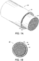
- Exemplary bias-able devices can have one or more functional layers provided upon a conductive substrate as shown in FIGS. 1A-1B , FIGS. 3A-3B and FIG. 4 in accordance with the present teachings.
- the rubber material can be used as one of the one or more functional layers to provide uniform mechanical and electrical functions.
- FIGS. 1A-1B depict an exemplary bias-able device 100 including a single-layer structure disposed upon a conductive substrate in accordance with the present teachings.
- FIG. 1A is a perspective view of a partial section of the exemplary bias-able device 100
- FIG. 1B is a cross-sectional view of the exemplary bias-able device 100 shown in FIG. 1A .
- the device depicted in FIGS. 1A-1B represents a generalized schematic illustration and that other layers/materials can be added or existing layers/materials can be removed or modified.
- the exemplary bias-able device 100 can include a conductive substrate 110, and a rubber material 120.
- the rubber material 120 can be disposed on the conductive substrate 110.
- the rubber material 120 can include, for example, a plurality of nanotubes 125 distributed throughout a rubber matrix 128.
- the conductive substrate 110 can be any conductive substrate as described herein.
- the size of the conductive substrate 110 can depend on the compliance of the rubber material, and more importantly, the size of the printing machine and the speed of the operation.
- the conductive substrate 110 can be a solid cylindrical shaft of stainless steel having a diameter of the cylindrical tube of about 1 mm to about 15 mm, and a length of about 10 mm to about 500 mm.
- the diameter of the conductive substrate 110 can be about 6 mm to about 15 mm and the length can be about 200 mm to about 500 mm.
- the diameter of the conductive substrate 110 can be less than about 6 mm and the length can be less than about 200 mm.
- the rubber material 120 can be disposed upon the surface of the conductive substrate 110.
- the rubber material 120 can be a conductive elastic layer configured to be responsible for the conformability (i.e., compliance) and the resistivity, which can be relative to the process speed and/or the AC frequency in the case of AC/DC condition. That is, the rubber material 120 can provide the nip-forming function and also relax the charge across the layer.
- the rubber material 120 can be prepared including one or more rubbers and a plurality of nanotubes as disclosed herein.
- the rubber material 120 can include a plurality of nanotubes 125 dispersed throughout a rubber matrix 128 as illustrated in FIG. 1A-1B .
- the plurality of nanotubes 125 can be oriented in a certain direction throughout the polymer matrix 128 for a desirable function.
- a plurality of carbon nanotubes such as SWCNTs can be dispersed physically or chemically throughout various rubber materials such as, for example, epichlorohydrins, urethanes, EPDM (ethylene propylene diene monomers), styrene-butadienes, silicones, chloroprenes, butyl rubbers, isoprenes, polyester thermoplastic rubbers, natural rubbers and the like.
- rubber materials such as, for example, epichlorohydrins, urethanes, EPDM (ethylene propylene diene monomers), styrene-butadienes, silicones, chloroprenes, butyl rubbers, isoprenes, polyester thermoplastic rubbers, natural rubbers and the like.
- the rubber material 120 including a plurality of nanotubes within a rubber matrix can be, for example, coated or cast on surface of the conductive substrate 110.
- the rubber material 120 can be, for example, extruded or molded to be accommodated with the configurations of the conductive substrate 110.
- the rubber material 120 can include rubbers that can be dissolved and cured or polymerized in situ on the surface of the conductive substrate 110 of the bias-able device 100.
- the rubber material 120 can include rubbers having relatively low melting points, which can be blended with biologically active materials and coated on the conductive substrate 110.
- the rubber material 120 can include biocompatible materials, enzymes and/or their biochemical reactions.
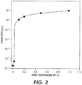
- the rubber material 120 can provide a desired resistivity, for example, ranging from about 10 5 ohm-cm to 10 10 ohm-cm. This resistivity range can be achieved with a low carbon-nanotube-loading such that the filler effect on compliance and other mechanical properties of the rubber used can be minimal and thus providing a wide material selection latitude. This is also because the electrical percolation of the rubber material 120 can be achieved by a very low carbon-nanotube-loading, for example, about 0.05 % by weight. In an exemplary embodiment, the carbon nanotube loading of the rubber material 120 can be about 2% by weight or less.
- FIG. 2 depicts an exemplary electrical result of a rubber material containing SWCNTs in accordance with the present teachings.
- the conductivity of the exemplary material can be about 10 -17 s/cm (10 17 ohm-cm).
- the conductivity of the material can be controlled by adding SWCNTs as conductive fillers to the rubber material.
- the conductivity of the rubber material can be about 10 -8 s/cm (10 8 ohm-cm), which can be a desired conductivity/ resistivity for the rubber material 120.
- Various conductivities/ resistivities or ranges of conductivity/ resistivity can be obtained and determined by the loading levels of the nanotubes (as indicated in FIG. 2 ) and/or the type of rubbers used.
- other functional layers can be added over the conductive substrate to meet, for example, the abrasion requirement, which can result in dual-, triple-, quad- or multiple-layered bias-able devices.
- the functional layers including the rubber material can provide desired mechanical, electrical, and surface functions for the bias-able devices in a manner that each of these functions can be separated and/or arbitrary combined in the discrete functional layers.
- the functional layers can include, but are not limited to, a compliant layer, a conductive elastic layer (e.g., the rubber material), an electroded layer, a resistance adjusting layer, a surface protecting layer, or any other functional layer.
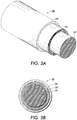
- FIGS. 3A-3B depict an exemplary bias-able device 300 having a dual-layer structure coated upon a conductive substrate in accordance with the present teachings.
- FIG. 3A is a perspective view in partial section of the exemplary bias-able device 300.
- FIG. 3B is a cross-sectional view of the exemplary bias-able device 300 shown in FIG. 3A . It should be readily apparent to one of ordinary skill in the art that the devices depicted in FIGS. 3A-3B represent a generalized schematic illustration and that other layers/materials can be added or existing layers/materials can be removed or modified.
- the exemplary bias-able device 300 can include a conductive substrate 310, a rubber material 320, and a surface material 330.
- the surface material 330 can be a surface resistive/protecting layer disposed on the rubber material 320 forming a dual-layer structure formed on the surface of the conductive substrate 310.
- the device 300 can be formed by simply disposing a surface layer on the rubber material 220 of the device 200.
- the conductive substrate 310 can use a substrate that is similar to the conductive substrate 110 as described in FIGS. 1A-1B .
- the rubber material 320 can be any rubber material as disclosed herein disposed upon the surface of the conductive substrate 310 to provide uniform mechanical and electrical properties for the bias-able device 300.
- the rubber material 320 can be prepared including a plurality of carbon nanotubes distributed within a rubber matrix.
- the rubber materials 320 can include SWCNTs dispersed uniformly throughout rubber matrices including, but not limited to, EPDM (ethylene propylene diene monomers), epichlorohydrins, urethanes, styrene-butadienes, silicones, chloroprenes, butyl rubbers, isoprenes, polyester thermoplastic rubbers, natural rubbers and the like.
- the rubber material 320 can include a plurality of SWCNTs with an exemplary weight loading of, for example, about 2.0% or less. In an additional example, the weight loading of SWCNTs can be about 0.1% or less.
- the surface material 330 can be disposed on the rubber material 320.
- the surface material 330 can be any surface material configured as a surface protecting layer and/or a resistivity adjusting layer known to one of ordinary skill in the art.
- the resistance of the surface material 330 can dominate the resistance of the bias-able devices 300, for example, a BCR, to reduce the electrical environmental instability of the entire BCR.
- the exemplary dual-layer bias-able device 300 can be used in both BCR and BTR applications.
- a BCR configured to charge the photoreceptor
- the first BTR can be configured at the nip interface of the photoreceptor and intermediate transfer belt
- the second BTR can be configured at the interface of intermediate transfer belt and, for example, paper.
- each material of the conductive substrate 310, the rubber material 320 and the surface material 330 can also depend on the machine architecture and the intended operating speed.
- the rubber material 320 can have a thickness of about 1-3 mm and provide a resistivity ranging from about 10 4 ohm-cm to about 10 8 ohm-cm at the operating field.
- the surface material 330 can have a thickness of about 0.01-0.1 mm and provide a resistivity of about 10 7 ohm-cm to about 10 11 ohm-cm.
- the rubber material 320 can have a thickness of about 3-5 mm and provide a resistivity ranging from about 10 5 ohm-cm to about 10 10 ohm-cm at the operating field.
- the surface material 330 can have a thickness of about 0.01-0.1 mm and provide a resistivity of about 10 8 to about 10 12 ohm-cm.
- the conductive substrate 310 can be, for example, a stainless steel shaft, and can have a diameter of about 8-12 mm.
- FIG. 4 depicts an exemplary bias-able device 400 having a triple-layer structure disposed upon a conductive substrate in accordance with the present teachings.
- FIG. 4 is a cross-sectional view of the exemplary bias-able device 400. It should be readily apparent to one of ordinary skill in the art that the devices depicted in FIG. 4 represents a generalized schematic illustration and that other layers/materials can be added or existing layers/materials can be removed or modified.
- the exemplary bias-able device 400 can include a conductive substrate 410, a conductive foam 415, a rubber material 420, and a surface material 430.
- the surface material 430 can be an outer layer disposed on the rubber material 420 disposed on the conductive foam 415 and form a triple-layer structure disposed on the surface of the conductive substrate 410.
- the conductive substrate 410 can be a substrate that is similar to the conductive substrate 110 and/or the conductive substrate 310 as described in FIGS. 1A-1B and/or FIG. 3 .
- the conductive substrate 410 can be, for example, a stainless steel shaft.
- the conductive foam 415 can be, for example, a conductive polyurethane foam to provide additional compliance for the device 400.
- the conductive foam 415 can be formed by, for example, molding the foam material according to the configuration of the conductive substrate 410.
- the rubber material 420 can be any disclosed rubber material disposed upon the surface of the conductive foam 415.
- the rubber material 420 can be similar to the rubber material 120 and/or 320 as described in FIGS. 1 and/or FIG. 3 to provide uniform mechanical and electrical properties for the bias-able device 400.
- the surface material 430 can be disposed on the rubber material 420.
- the surface material 430 can be any surface material configured as a surface protecting and/or resistivity adjusting layer known to one of ordinary skill in the art.
- the device 400 can have a large size for each layer and can be more compliant.
- the bias-able device 400 can be used for an application of the second BTR for the exemplary 4-cycle color engine.
- the conductive substrate 410 can be, for example, a stainless steel shaft, and can have a diameter of about 10 mm to about 15 mm.
- the conductive foam 415 can have a thickness of, for example, about 3 mm to about 5 mm.
- the rubber material 420 can have a thickness of about 3 mm to about 5 mm.
Landscapes
- Physics & Mathematics (AREA)
- General Physics & Mathematics (AREA)
- Engineering & Computer Science (AREA)
- Plasma & Fusion (AREA)
- Electrostatic Charge, Transfer And Separation In Electrography (AREA)
- Rolls And Other Rotary Bodies (AREA)
- Compositions Of Macromolecular Compounds (AREA)
- Electrophotography Configuration And Component (AREA)
Claims (9)
- Dispositif électriquement polarisable (300) comprenant :une âme électriquement conductrice (310) ;un matériau de type caoutchouc (320) disposé par-dessus l'âme électriquement conductrice et l'entourant, dans lequel le matériau de type caoutchouc comprend une pluralité de nanotubes dispersés à travers une matrice en caoutchouc, en une quantité propre à conférer au matériau de type caoutchouc une première résistivité électrique et une conformabilité mécanique ;dans lequel un matériau de surface (330) est disposé par-dessus le matériau de type caoutchouc (320) et l'entoure,dans lequel le matériau de surface présente une seconde résistivité électrique et une surface protectrice,dans lequel une résistance du matériau de surface (330) domine la résistance des dispositifs électriquement polarisables (300), etdans lequel la pluralité de nanotubes comprend des nanotubes de carbone monofeuillets (SWCNT, single wall carbone nanotubes) ayant une charge en poids de moins de 0,1 % à travers la matrice en caoutchouc.
- Dispositif (300) selon la revendication 1, dans lequel le dispositif électriquement polarisable (300) est soit un rouleau de charge de polarisation (BCR, bias charging roll) soit un rouleau de transfert de polarisation (BTR, bias transfer roll).
- Dispositif (300) selon la revendication 1 ou 2, dans lequel l'âme électriquement conductrice (310) présente une forme choisie dans le groupe composé d'une âme, d'une courroie et d'un film.
- Dispositif (300) selon l'une quelconque des revendications 1 à 3, dans lequel l'âme électriquement conductrice (310) comprend un arbre en acier inoxydable présentant un diamètre de 6 mm à 15 mm et une longueur de 200 mm à 500 mm.
- Dispositif (300) selon l'une des revendications 1 à 4, dans lequel le matériau de type caoutchouc (320) possède une résistivité électrique de 105 ohm-cm à 1010 ohm-cm et le matériau de surface (330) possède une résistivité électrique de 108 ohm-cm à 1012 ohm-cm.
- Dispositif (300) selon la revendication 1, dans lequel la pluralité de nanotubes comprend des nanotubes de carbone multifeuillets.
- Dispositif (300) selon la revendication 1, dans lequel la pluralité de nanotubes présente une forme en coupe transversale choisie dans le groupe composé d'un polygone, d'un rectangle, d'un carré, d'un ovale et d'un cercle.
- Imprimante électrostatographique comprenant le dispositif électriquement polarisable selon l'une quelconque des revendications 1 à 7.
- Procédé pour former un dispositif électriquement polarisable, comprenant les étapes suivantes :utiliser une âme électriquement conductrice (310) ;former un matériau de type caoutchouc (320) en dispersant une pluralité de nanotubes à l'intérieur d'une matrice en caoutchouc, dans lequel la pluralité de nanotubes confère au matériau de type caoutchouc une résistivité électrique et une conformabilité mécanique ;disposer le matériau de type caoutchouc (320) comportant la pluralité de nanotubes sur l'âme électriquement conductrice, etdisposer un matériau de surface (330) par-dessus le matériau de type caoutchouc (320) et en l'entourant, dans lequel le matériau de surface (330) présente une seconde résistivité électrique et une surface protectrice,dans lequel une résistance du matériau de surface (330) domine la résistance des dispositifs électriquement polarisables (300), etdans lequel la pluralité de nanotubes comprend des nanotubes de carbone monofeuillets (SWCNT, single wall carbone nanotubes) ayant une charge en poids de moins de 0,1 % à travers la matrice en caoutchouc.
Applications Claiming Priority (1)
| Application Number | Priority Date | Filing Date | Title |
|---|---|---|---|
| US11/688,604 US8099023B2 (en) | 2007-03-20 | 2007-03-20 | Conformable, electrically relaxable rubbers using carbon nanotubes for BCR/BTR applications |
Publications (3)
| Publication Number | Publication Date |
|---|---|
| EP1973010A2 EP1973010A2 (fr) | 2008-09-24 |
| EP1973010A3 EP1973010A3 (fr) | 2012-10-10 |
| EP1973010B1 true EP1973010B1 (fr) | 2018-04-11 |
Family
ID=39434282
Family Applications (1)
| Application Number | Title | Priority Date | Filing Date |
|---|---|---|---|
| EP08151794.8A Ceased EP1973010B1 (fr) | 2007-03-20 | 2008-02-22 | Caoutchoucs à relâchement électrique, confortable, utilisant des nanotubes de carbone pour des applications BCR/BTR |
Country Status (4)
| Country | Link |
|---|---|
| US (1) | US8099023B2 (fr) |
| EP (1) | EP1973010B1 (fr) |
| JP (1) | JP2008233904A (fr) |
| CA (1) | CA2625443C (fr) |
Families Citing this family (8)
| Publication number | Priority date | Publication date | Assignee | Title |
|---|---|---|---|---|
| JP5236271B2 (ja) * | 2007-12-10 | 2013-07-17 | 株式会社イノアックコーポレーション | 導電性ポリウレタンフォーム及びその製造方法並びに導電性ローラ |
| KR101518735B1 (ko) * | 2009-02-19 | 2015-05-18 | 삼성전자주식회사 | 탄소나노튜브를 채용한 가열 부재 및 이를 채용한 정착장치 |
| US8099035B2 (en) * | 2009-11-16 | 2012-01-17 | Xerox Corporation | Induction heated member |
| US8649704B2 (en) * | 2009-11-20 | 2014-02-11 | Xerox Corporation | Bias charging overcoat |
| US20110275502A1 (en) * | 2010-05-10 | 2011-11-10 | 7-Sigma, Inc. | Electrically conductive member for electrophotographic printer applications |
| US8349942B2 (en) * | 2011-05-10 | 2013-01-08 | Xerox Corporation | Intermediate transfer member |
| US8753735B2 (en) * | 2011-06-15 | 2014-06-17 | Xerox Corporation | Bias charge roller surface coating comprised of carbon nanotubes |
| WO2013163549A1 (fr) | 2012-04-26 | 2013-10-31 | The University Of Akron | Capteurs tactiles flexibles et leur procédé de fabrication |
Citations (2)
| Publication number | Priority date | Publication date | Assignee | Title |
|---|---|---|---|---|
| US6016418A (en) * | 1994-02-14 | 2000-01-18 | Canon Kabushiki Kaisha | Image forming apparatus |
| EP1288730A1 (fr) * | 2001-08-28 | 2003-03-05 | Seiko Epson Corporation | Appareil de formation d'images |
Family Cites Families (15)
| Publication number | Priority date | Publication date | Assignee | Title |
|---|---|---|---|---|
| JP3080126B2 (ja) | 1993-07-30 | 2000-08-21 | キヤノン株式会社 | 帯電部材、プロセスカートリッジ及び画像形成装置 |
| US6141516A (en) * | 1996-06-28 | 2000-10-31 | Xerox Corporation | Fluorinated carbon filled fluoroelastomer outer layer |
| JP2000137369A (ja) * | 1998-10-30 | 2000-05-16 | Tokai Rubber Ind Ltd | 帯電ロール |
| US6160980A (en) * | 1999-11-10 | 2000-12-12 | Ziegelmuller; Francisco Luiz | Method and apparatus for reducing contamination of a tackdown, capture or transfer roller on a spliced photoconductor or transport web |
| JP2001215859A (ja) * | 1999-11-26 | 2001-08-10 | Canon Inc | 画像形成装置 |
| JP2005284295A (ja) * | 2000-03-29 | 2005-10-13 | Kinugawa Rubber Ind Co Ltd | 半導電性ローラ |
| JP2004094161A (ja) | 2002-09-04 | 2004-03-25 | Mitsubishi Cable Ind Ltd | 帯電ローラ |
| JP4227786B2 (ja) * | 2002-09-10 | 2009-02-18 | 住友ゴム工業株式会社 | 導電性ローラおよび該導電性ローラの製造方法 |
| US20040086305A1 (en) * | 2002-10-31 | 2004-05-06 | Samsung Electronics Co. Ltd. | Image transfer belt having a polymeric coating on a conductive substrate on a polymeric film |
| JP2004205592A (ja) * | 2002-12-24 | 2004-07-22 | Inoac Corp | 導電ローラ |
| JP4196780B2 (ja) * | 2003-08-12 | 2008-12-17 | 東海ゴム工業株式会社 | 電子写真機器用導電性組成物の製法 |
| JP2005220316A (ja) | 2004-02-09 | 2005-08-18 | Tokai Rubber Ind Ltd | 電子写真機器用導電性組成物およびその製法、ならびにそれを用いた電子写真機器用導電性部材 |
| KR100683180B1 (ko) | 2005-06-23 | 2007-02-15 | 삼성전자주식회사 | 탄소나노튜브를 포함하는 전자사진장치용 현상 롤러 및 그제조 방법 |
| JP2007023149A (ja) * | 2005-07-15 | 2007-02-01 | National Institute Of Advanced Industrial & Technology | 導電性が制御されたカーボンナノチューブ分散ポリイミド |
| JP2007108468A (ja) * | 2005-10-14 | 2007-04-26 | Ricoh Co Ltd | 帯電部材、帯電装置及び画像形成装置 |
-
2007
- 2007-03-20 US US11/688,604 patent/US8099023B2/en not_active Expired - Fee Related
-
2008
- 2008-02-22 EP EP08151794.8A patent/EP1973010B1/fr not_active Ceased
- 2008-03-13 CA CA2625443A patent/CA2625443C/fr not_active Expired - Fee Related
- 2008-03-13 JP JP2008064567A patent/JP2008233904A/ja active Pending
Patent Citations (2)
| Publication number | Priority date | Publication date | Assignee | Title |
|---|---|---|---|---|
| US6016418A (en) * | 1994-02-14 | 2000-01-18 | Canon Kabushiki Kaisha | Image forming apparatus |
| EP1288730A1 (fr) * | 2001-08-28 | 2003-03-05 | Seiko Epson Corporation | Appareil de formation d'images |
Also Published As
| Publication number | Publication date |
|---|---|
| US20080232853A1 (en) | 2008-09-25 |
| US8099023B2 (en) | 2012-01-17 |
| EP1973010A3 (fr) | 2012-10-10 |
| JP2008233904A (ja) | 2008-10-02 |
| CA2625443A1 (fr) | 2008-09-20 |
| CA2625443C (fr) | 2015-01-27 |
| EP1973010A2 (fr) | 2008-09-24 |
Similar Documents
| Publication | Publication Date | Title |
|---|---|---|
| EP1973010B1 (fr) | Caoutchoucs à relâchement électrique, confortable, utilisant des nanotubes de carbone pour des applications BCR/BTR | |
| JP3639773B2 (ja) | 半導電性ゴム組成物、帯電部材、電子写真装置、プロセスカートリッジ | |
| US9818947B2 (en) | Semiconductive roller of an image-forming apparatus | |
| JP2009155506A (ja) | 導電性エラストマー材料、該材料からなる導電性シートおよび導電性シームレスベルト | |
| JP3951860B2 (ja) | 電子写真装置半導電性部材用の半導電性高分子弾性部材およびそれを用いた半導電性部材、ならびに電子写真装置半導電性部材用の半導電性高分子弾性部材の製法 | |
| US20160041491A1 (en) | Electroconductive roller, and image forming apparatus | |
| JP2003156902A (ja) | 画像形成装置用ベルト、スリーブ又はチューブ | |
| CN1371031A (zh) | 导电橡胶辊 | |
| JP2000006260A (ja) | 導電性ベルト及び導電性ローラ | |
| JP3763917B2 (ja) | 低硬度ゴムロールおよびその製造方法 | |
| JP7247017B2 (ja) | キャリア層付きシームレスベルト、その製造方法及び画像形成装置用弾性層付き転写ベルトの製造方法 | |
| JP3070556B2 (ja) | 導電ロール | |
| JP3320001B2 (ja) | 導電ロールの製造方法 | |
| EP2353874B1 (fr) | Appareil de transport de support et appareil d'enregistrement à jet d'encre | |
| JP3535789B2 (ja) | 導電性弾性体及びそれを用いた画像形成装置 | |
| JP4451677B2 (ja) | 表面保護層付きシームレスベルト及びその製造方法 | |
| JP3100625B2 (ja) | 導電ロール及びその導電ロールの製造方法 | |
| JP3328969B2 (ja) | シームレスベルトおよびその製造方法 | |
| JP3070557B2 (ja) | 導電ロール | |
| JP5242026B2 (ja) | 接触式帯電/除電用導電シート | |
| JP5060760B2 (ja) | 導電性ゴムローラー及び画像形成装置 | |
| JP2001132858A (ja) | 現像ロ−ラ | |
| JP2005141115A (ja) | 半導電性ローラ及び電子写真装置 | |
| JP2001175085A (ja) | 転写ベルト | |
| JP2003098818A (ja) | 現像剤担持体及び現像装置 |
Legal Events
| Date | Code | Title | Description |
|---|---|---|---|
| PUAI | Public reference made under article 153(3) epc to a published international application that has entered the european phase |
Free format text: ORIGINAL CODE: 0009012 |
|
| AK | Designated contracting states |
Kind code of ref document: A2 Designated state(s): AT BE BG CH CY CZ DE DK EE ES FI FR GB GR HR HU IE IS IT LI LT LU LV MC MT NL NO PL PT RO SE SI SK TR |
|
| AX | Request for extension of the european patent |
Extension state: AL BA MK RS |
|
| PUAL | Search report despatched |
Free format text: ORIGINAL CODE: 0009013 |
|
| AK | Designated contracting states |
Kind code of ref document: A3 Designated state(s): AT BE BG CH CY CZ DE DK EE ES FI FR GB GR HR HU IE IS IT LI LT LU LV MC MT NL NO PL PT RO SE SI SK TR |
|
| AX | Request for extension of the european patent |
Extension state: AL BA MK RS |
|
| RIC1 | Information provided on ipc code assigned before grant |
Ipc: G03G 15/16 20060101AFI20120906BHEP Ipc: G03G 15/02 20060101ALI20120906BHEP |
|
| 17P | Request for examination filed |
Effective date: 20130410 |
|
| AKX | Designation fees paid |
Designated state(s): DE FR GB |
|
| 17Q | First examination report despatched |
Effective date: 20170724 |
|
| GRAP | Despatch of communication of intention to grant a patent |
Free format text: ORIGINAL CODE: EPIDOSNIGR1 |
|
| INTG | Intention to grant announced |
Effective date: 20180108 |
|
| GRAS | Grant fee paid |
Free format text: ORIGINAL CODE: EPIDOSNIGR3 |
|
| GRAA | (expected) grant |
Free format text: ORIGINAL CODE: 0009210 |
|
| AK | Designated contracting states |
Kind code of ref document: B1 Designated state(s): DE FR GB |
|
| REG | Reference to a national code |
Ref country code: GB Ref legal event code: FG4D |
|
| REG | Reference to a national code |
Ref country code: DE Ref legal event code: R096 Ref document number: 602008054753 Country of ref document: DE |
|
| REG | Reference to a national code |
Ref country code: DE Ref legal event code: R097 Ref document number: 602008054753 Country of ref document: DE |
|
| PLBE | No opposition filed within time limit |
Free format text: ORIGINAL CODE: 0009261 |
|
| STAA | Information on the status of an ep patent application or granted ep patent |
Free format text: STATUS: NO OPPOSITION FILED WITHIN TIME LIMIT |
|
| 26N | No opposition filed |
Effective date: 20190114 |
|
| PGFP | Annual fee paid to national office [announced via postgrant information from national office to epo] |
Ref country code: GB Payment date: 20200123 Year of fee payment: 13 |
|
| PGFP | Annual fee paid to national office [announced via postgrant information from national office to epo] |
Ref country code: FR Payment date: 20200122 Year of fee payment: 13 |
|
| GBPC | Gb: european patent ceased through non-payment of renewal fee |
Effective date: 20210222 |
|
| PG25 | Lapsed in a contracting state [announced via postgrant information from national office to epo] |
Ref country code: FR Free format text: LAPSE BECAUSE OF NON-PAYMENT OF DUE FEES Effective date: 20210228 Ref country code: GB Free format text: LAPSE BECAUSE OF NON-PAYMENT OF DUE FEES Effective date: 20210222 |
|
| PGFP | Annual fee paid to national office [announced via postgrant information from national office to epo] |
Ref country code: DE Payment date: 20220119 Year of fee payment: 15 |
|
| REG | Reference to a national code |
Ref country code: DE Ref legal event code: R119 Ref document number: 602008054753 Country of ref document: DE |
|
| PG25 | Lapsed in a contracting state [announced via postgrant information from national office to epo] |
Ref country code: DE Free format text: LAPSE BECAUSE OF NON-PAYMENT OF DUE FEES Effective date: 20230901 |