EP1965612B1 - Entladelampen-beleuchtungsvorrichtung und bildanzeigevorrichtung - Google Patents
Entladelampen-beleuchtungsvorrichtung und bildanzeigevorrichtung Download PDFInfo
- Publication number
- EP1965612B1 EP1965612B1 EP06843020A EP06843020A EP1965612B1 EP 1965612 B1 EP1965612 B1 EP 1965612B1 EP 06843020 A EP06843020 A EP 06843020A EP 06843020 A EP06843020 A EP 06843020A EP 1965612 B1 EP1965612 B1 EP 1965612B1
- Authority
- EP
- European Patent Office
- Prior art keywords
- discharge lamp
- switching
- lighting device
- lamp lighting
- switching frequency
- Prior art date
- Legal status (The legal status is an assumption and is not a legal conclusion. Google has not performed a legal analysis and makes no representation as to the accuracy of the status listed.)
- Ceased
Links
- 230000004044 response Effects 0.000 claims description 16
- 230000010355 oscillation Effects 0.000 claims description 8
- 230000003287 optical effect Effects 0.000 claims description 5
- 230000005540 biological transmission Effects 0.000 claims description 4
- 238000005259 measurement Methods 0.000 claims description 2
- 230000001172 regenerating effect Effects 0.000 description 14
- 230000014509 gene expression Effects 0.000 description 9
- 238000001514 detection method Methods 0.000 description 7
- 238000010586 diagram Methods 0.000 description 5
- 230000006870 function Effects 0.000 description 4
- 239000003990 capacitor Substances 0.000 description 3
- 238000006243 chemical reaction Methods 0.000 description 3
- 238000001816 cooling Methods 0.000 description 2
- 230000003247 decreasing effect Effects 0.000 description 2
- 230000000694 effects Effects 0.000 description 2
- 238000004804 winding Methods 0.000 description 2
- 238000005562 fading Methods 0.000 description 1
- 239000004973 liquid crystal related substance Substances 0.000 description 1
- 238000012544 monitoring process Methods 0.000 description 1
- 230000003071 parasitic effect Effects 0.000 description 1
Images


Classifications
-
- H—ELECTRICITY
- H05—ELECTRIC TECHNIQUES NOT OTHERWISE PROVIDED FOR
- H05B—ELECTRIC HEATING; ELECTRIC LIGHT SOURCES NOT OTHERWISE PROVIDED FOR; CIRCUIT ARRANGEMENTS FOR ELECTRIC LIGHT SOURCES, IN GENERAL
- H05B41/00—Circuit arrangements or apparatus for igniting or operating discharge lamps
- H05B41/14—Circuit arrangements
- H05B41/26—Circuit arrangements in which the lamp is fed by power derived from DC by means of a converter, e.g. by high-voltage DC
- H05B41/28—Circuit arrangements in which the lamp is fed by power derived from DC by means of a converter, e.g. by high-voltage DC using static converters
- H05B41/288—Circuit arrangements in which the lamp is fed by power derived from DC by means of a converter, e.g. by high-voltage DC using static converters with semiconductor devices and specially adapted for lamps without preheating electrodes, e.g. for high-intensity discharge lamps, high-pressure mercury or sodium lamps or low-pressure sodium lamps
- H05B41/2881—Load circuits; Control thereof
- H05B41/2882—Load circuits; Control thereof the control resulting from an action on the static converter
-
- G—PHYSICS
- G03—PHOTOGRAPHY; CINEMATOGRAPHY; ANALOGOUS TECHNIQUES USING WAVES OTHER THAN OPTICAL WAVES; ELECTROGRAPHY; HOLOGRAPHY
- G03B—APPARATUS OR ARRANGEMENTS FOR TAKING PHOTOGRAPHS OR FOR PROJECTING OR VIEWING THEM; APPARATUS OR ARRANGEMENTS EMPLOYING ANALOGOUS TECHNIQUES USING WAVES OTHER THAN OPTICAL WAVES; ACCESSORIES THEREFOR
- G03B21/00—Projectors or projection-type viewers; Accessories therefor
- G03B21/14—Details
- G03B21/20—Lamp housings
- G03B21/2006—Lamp housings characterised by the light source
- G03B21/2026—Gas discharge type light sources, e.g. arcs
-
- H—ELECTRICITY
- H02—GENERATION; CONVERSION OR DISTRIBUTION OF ELECTRIC POWER
- H02M—APPARATUS FOR CONVERSION BETWEEN AC AND AC, BETWEEN AC AND DC, OR BETWEEN DC AND DC, AND FOR USE WITH MAINS OR SIMILAR POWER SUPPLY SYSTEMS; CONVERSION OF DC OR AC INPUT POWER INTO SURGE OUTPUT POWER; CONTROL OR REGULATION THEREOF
- H02M3/00—Conversion of DC power input into DC power output
- H02M3/02—Conversion of DC power input into DC power output without intermediate conversion into AC
- H02M3/04—Conversion of DC power input into DC power output without intermediate conversion into AC by static converters
- H02M3/10—Conversion of DC power input into DC power output without intermediate conversion into AC by static converters using discharge tubes with control electrode or semiconductor devices with control electrode
- H02M3/145—Conversion of DC power input into DC power output without intermediate conversion into AC by static converters using discharge tubes with control electrode or semiconductor devices with control electrode using devices of a triode or transistor type requiring continuous application of a control signal
- H02M3/155—Conversion of DC power input into DC power output without intermediate conversion into AC by static converters using discharge tubes with control electrode or semiconductor devices with control electrode using devices of a triode or transistor type requiring continuous application of a control signal using semiconductor devices only
- H02M3/156—Conversion of DC power input into DC power output without intermediate conversion into AC by static converters using discharge tubes with control electrode or semiconductor devices with control electrode using devices of a triode or transistor type requiring continuous application of a control signal using semiconductor devices only with automatic control of output voltage or current, e.g. switching regulators
- H02M3/157—Conversion of DC power input into DC power output without intermediate conversion into AC by static converters using discharge tubes with control electrode or semiconductor devices with control electrode using devices of a triode or transistor type requiring continuous application of a control signal using semiconductor devices only with automatic control of output voltage or current, e.g. switching regulators with digital control
-
- H—ELECTRICITY
- H05—ELECTRIC TECHNIQUES NOT OTHERWISE PROVIDED FOR
- H05B—ELECTRIC HEATING; ELECTRIC LIGHT SOURCES NOT OTHERWISE PROVIDED FOR; CIRCUIT ARRANGEMENTS FOR ELECTRIC LIGHT SOURCES, IN GENERAL
- H05B41/00—Circuit arrangements or apparatus for igniting or operating discharge lamps
- H05B41/14—Circuit arrangements
- H05B41/26—Circuit arrangements in which the lamp is fed by power derived from DC by means of a converter, e.g. by high-voltage DC
- H05B41/28—Circuit arrangements in which the lamp is fed by power derived from DC by means of a converter, e.g. by high-voltage DC using static converters
- H05B41/288—Circuit arrangements in which the lamp is fed by power derived from DC by means of a converter, e.g. by high-voltage DC using static converters with semiconductor devices and specially adapted for lamps without preheating electrodes, e.g. for high-intensity discharge lamps, high-pressure mercury or sodium lamps or low-pressure sodium lamps
- H05B41/2885—Static converters especially adapted therefor; Control thereof
-
- Y—GENERAL TAGGING OF NEW TECHNOLOGICAL DEVELOPMENTS; GENERAL TAGGING OF CROSS-SECTIONAL TECHNOLOGIES SPANNING OVER SEVERAL SECTIONS OF THE IPC; TECHNICAL SUBJECTS COVERED BY FORMER USPC CROSS-REFERENCE ART COLLECTIONS [XRACs] AND DIGESTS
- Y02—TECHNOLOGIES OR APPLICATIONS FOR MITIGATION OR ADAPTATION AGAINST CLIMATE CHANGE
- Y02B—CLIMATE CHANGE MITIGATION TECHNOLOGIES RELATED TO BUILDINGS, e.g. HOUSING, HOUSE APPLIANCES OR RELATED END-USER APPLICATIONS
- Y02B20/00—Energy efficient lighting technologies, e.g. halogen lamps or gas discharge lamps
Definitions
- the present invention relates to a discharge lamp lighting device that lights a discharge lamp, and to an image display device using the discharge lamp lighting device.
- This discharge lamp lighting device 100 is composed of a power supply circuit unit 101 and a lighting control circuit unit 102.
- the power supply circuit unit 101 is, for example, a chopper circuit.
- the power supply circuit unit 101 is composed of a direct current power supply E, a load 109, a switching element Q, a resistor R for detecting a current flowing through the switching element Q, a power transformer T, a diode D, a capacitor C, and a load voltage detector 103 that detects a voltage of the load 109.
- the switching element Q of the power supply circuit unit 101 performs a switching operation by a drive signal outputted from a drive controller 108 of the lighting control circuit unit 102 in response to a state (power, voltage and the like) of the load 109.
- the lighting control circuit unit 102 is composed of a zero cross detector 104 that is connected to a secondary side of the power transformer T and detects that a secondary current has turned to zero, a current detector 105 that compares, in terms of magnitude, the current flowing through the switching element Q and a reference value Is corresponding to power of the load 109 with each other, a reference arithmetic unit 106 that outputs the reference value Is in response to the power of the load 109, an A/D converter 107 that performs A/D conversion for the load voltage detected by the load voltage detector 103, and the drive controller 108 that controls on/off of the switching element Q.
- the drive controller 108 is composed, for example, by having an RS flip-flop and the like.
- a current of the power transformer T during an on-time Ton while the switching element Q is being turned on, as shown in FIG. 12A , energy is charged to the power transformer T, and the current of the power transformer T is increased.
- a regenerative current that releases the energy stored in the power transformer T flows through the capacitor C and the diode D, and is gradually decreased.
- the current of the power transformer T turns to zero.
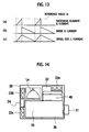
- the zero cross detector 104 When it is detected that the energy stored in the power transformer T has turned to zero by the zero cross detector 104 of the lighting control circuit unit 102, as shown in FIG. 12C , the zero cross detector 104 inputs a turn-on signal of the switching element Q to a set input terminal SET of the drive controller 108. The drive controller 108 turns on the switching element Q.
- the load voltage Vla is detected by the load voltage detector 103, and the load voltage Vla concerned is monitored by the reference arithmetic unit 106 through the A/D converter 107, whereby the reference voltage arithmetic unit 106 outputs the reference value Is corresponding to the power of the load 109.
- the current detector 105 compares a value detected by the resistor R from the current flowing through the switching element Q and a value of the reference value Is with each other. When the detected value of the current flowing through the switching element Q becomes more than the reference value Is, as shown in FIG. 12D , the current detector 105 outputs a detection signal to a reset input terminal RESET of the drive controller 108, and the drive controller 108 turns off the switching element Q.
- FIG. 12D the current detector 105 outputs a detection signal to a reset input terminal RESET of the drive controller 108, and the drive controller 108 turns off the switching element Q.
- the discharge lamp lighting device can supply the appropriate power corresponding to the load voltage Vla, and moreover, can control the switching element Q to turn on at timing when the current flowing through the transistor T makes a zero cross.
- Patent Document 1 Japanese Patent Laid-Open Publication No. 2004-178925 .
- This discharge lamp lighting device includes an off-time timer circuit that counts an off-time of the chopper, and includes a zero cross detector that, when a predetermined time is counted by the off-time timer circuit before detecting the energy release of the chopper coil, detects the energy release of the chopper coil while turns on the chopper at timing when the predetermined time is counted.
- the discharge lamp lighting device In the case of controlling the switching element Q to turn on at the timing of the zero cross of the current by the power supply circuit unit using the chopper circuit, which is shown in FIG. 11 , the discharge lamp lighting device requires an operation to detect that the energy stored in the power transformer T has turned to zero. Accordingly, this discharge lamp lighting device requires zero cross detection using a secondary winding of the power transformer T, and has a problem that the number of parts is increased, bringing up a cost increase.
- an operation frequency in the case of controlling the switching element Q to turn on by the zero cross detection is decided by self-excitation by an input voltage Vin of the direct current power supply E, the load voltage Vla, load power, and an inductance value of the power transformer T. Accordingly, when the load voltage Vla of a discharge lamp is changed with time, a switching frequency is changed as shown by a broken line of FIG. 5 . When noise of the switching frequency is superimposed on the load current, and a ripple component by the noise is superimposed on a frequency-prohibited range intrinsic to the load, there is also a problem that such a ripple cannot be avoided.
- the load 109 is a high-voltage discharge lamp
- the frequency-prohibited range intrinsic to the load there is a range where an acoustic resonance phenomenon occurs, and there is an apprehension to bring up instability, fading, flickering and the like of arcs.
- US 6,288,501 discloses a ballast for a discharge lamp with a converter including a switching element and an energy storing element, wherein the switching element is controlled to operate for repetitively switching the DC voltage from the same source voltage in order to store energy in the energy storing element.
- a controller provides a command value and turns on and off the switching element for variable periods in accordance with command value for generating a necessary power to the them.
- US 5,859,505 discloses a controller for operating a discharge lamp at high frequencies to avoid arc date instabilities by operating it at different operating frequencies so that it stays longer at frequencies which are stable while only staying for short times at frequencies where the arc is unstable.
- the present invention has been made in consideration for the points as described above. It is an object of the present invention to control the operation frequency of the switching element in response to a state of the discharge lamp without binging up the cost increase of the discharge lamp lighting device, thus making it possible to control such on-timing of the switching element to be timing when the regenerative current turns to zero.
- Claims 2 to 5 refer to specifically advantageous realizations of the subject matter of claim 1.
- a first aspect of the invention is a discharge lamp lighting device including a switching circuit 2 that controls power supplied to a discharge lamp La, in which, in the switching circuit 2, a switching frequency is controlled in response to a state of the discharge lamp La, energy stored in an inductance component L when a switching element Q is turned on is released when the switching element Q is turned off, and the switching element Q is controlled to turn on at timing when a current for releasing the energy turns to substantial zero
- the discharge lamp lighting device comprising: a load voltage detector 5 that detects a load voltage Vla; a switching frequency counting unit 8 that performs time measurement for setting the switching frequency based on the voltage detected from the load voltage detector 5 so that predetermined power of the discharge lamp can be achieved; a current detector 6 that detects that the current flowing through the switching circuit 2 has reached a predetermined reference value Is; a reference arithmetic unit 7 that sets the predetermined reference value Is based on the voltage detected from the load voltage detector
- the switching frequency of the switching element is set in response to the load voltage, and the timing when the switching element is turned on is set by the switching frequency counting unit so as to achieve the switching frequency. Then, the reference value of the current, which decides the timing when the switching element is turned off, is set by the reference arithmetic unit so that the timing when the current for releasing the energy while the switching element is being turned off turns to substantially zero at the switching frequency thus set can just coincide with the next timing when the switching element is turned on.
- the operation frequency of the switching element is controlled in response to the state of the discharge lamp without using the zero cross detection circuit, thus making it possible to control the timing when the switching element is turned on at the timing when the regenerative current turns to substantial zero.
- the zero cross detection circuit becomes unnecessary, whereby the number of parts is reduced, and a cost increase of the discharge lamp lighting device can be prevented or suppressed.
- a second aspect of the invention is the discharge lamp lighting device in the first aspect of the invention, further comprising: an input voltage detector 12 that detects an input voltage Vin of the switching circuit 2, wherein, based on the input voltage Vin detected from the input voltage detector 12 and the load voltage Vla detected from the load voltage detector 5, the switching frequency and the predetermined reference value Is are set so that the predetermined power of the discharge lamp can be achieved.
- the switching element can be operated to turn on at the timing when the regenerative current of the switching circuit turns to substantial zero.
- a third aspect of the invention is the discharge lamp lighting device in the first or second aspects of the invention, wherein the switching frequency and the predetermined reference value are set so that the switching element Q can turn on at timing of a peak voltage of a free oscillation voltage generated when the current for releasing the energy becomes substantially zero.
- the switching element turns on at timing when the voltage at the time when the switching element is off turns to substantial minimum. Accordingly, a switching loss can be reduced.
- a fourth aspect of the invention is the discharge lamp lighting device according to any one of the first to third aspects of the inventions, wherein, as shown in FIG. 6 to FIG. 10 , when the switching frequency set based on the voltage detected from the load voltage detector 5 is superimposed on an operation-prohibited range (an acoustic resonance frequency range and a frequency range where an occurrence of noise becomes a problem), the switching frequency counting unit 8 sets the switching frequency at a fixed frequency other than the operation-prohibited range.
- an operation-prohibited range an acoustic resonance frequency range and a frequency range where an occurrence of noise becomes a problem
- the switching operation in the frequency range where an acoustic resonance of the high-voltage discharge lamp occurs and in the frequency range where the occurrence of the noise becomes a problem can be avoided.
- a fifth aspect of the invention is an image display device, comprising: the discharge lamp lighting device in any one of the first to fourth aspect of the inventions; a discharge lamp turned on by the discharge lamp lighting device; image display means for transmitting therethrough or reflecting thereon light from the discharge lamp; and an optical system that projects transmission light or reflection light, which passes through the image display means, on a screen.
- FIG. 1 is a circuit diagram showing a configuration of a discharge lamp lighting device according to Embodiment 1 of the present invention.
- the discharge lamp lighting device 1 is composed of a switching circuit 2 and a control circuit 3 thereof.
- the switching circuit 2 includes a direct current power supply E, a switching element Q, a choke coil L, a diode D, a capacitor C, and a resistor R.
- the switching circuit 2 is composed as a step-down chopper circuit.
- the switching element Q is composed, for example, of a MOSFET, turns on/off by a signal outputted from the control circuit 3, and performs switching so as to appropriately adjust power of a load.
- the control circuit 3 controls the switching element Q to turn on/off so as to appropriately adjust the power of a discharge lamp La.
- the control circuit 3 is composed of a current detector 6, a reference arithmetic unit 7, a switching frequency counting unit 8, a drive controller 9, an A/D converter 10.
- the reference arithmetic unit 7, the switching frequency counting unit 8 and the A/D converter 10 are mounted in a microcomputer 4.
- the current detector 6 compares, in terms of magnitude, a voltage value detected by the resistor R from a current flowing through the switching element Q and a reference value Is outputted from the reference arithmetic unit 7 in response to the power of the discharge lamp La with each other, and outputs an off signal of the switching element Q.
- the A/D converter 10 converts a load voltage Vla (analog value) detected by a load voltage detector 5 into a digital signal with predetermined bits.
- the reference arithmetic unit 7 is composed of the microcomputer 4 and the like.
- the reference arithmetic unit 7 outputs the reference value Is based on the load voltage subjected to the A/D conversion. This reference value Is is compared in terms of the magnitude with the current flowing through the switching element Q by the current detector 6.
- the switching frequency counting unit 8 is composed of the microcomputer 4 and the like.
- the switching frequency counting unit 8 outputs an on signal of the switching element Q to the drive controller 9 based on the load voltage subjected to the A/D conversion. This on signal is outputted at timing when a regenerative current flowing through the diode D turns to zero.
- the drive controller 9 is composed by using an RS flip-flop and the like.
- the drive controller 9 receives a turn-on signal, which is outputted from the switching frequency counting unit 8, to a set input terminal SET side, and receives a turn-off signal, which is outputted from the current detector 6, to a reset input terminal RESET side.
- the drive controller 9 controls the switching element Q to turn on/off at the timing when the regenerative current turns to zero as shown in FIG. 13 , thereby appropriately adjusting the power of the discharge lamp La.
- the reference value Is of the reference arithmetic unit 7 and the switching frequency of the switching frequency counting unit 8 are obtained by using an input voltage Vin from the direct current power supply E, input power Pin therefrom, an inductance value L of the choke coil composing the chopper circuit and the load voltage Vla. From the following Expressions (1) to (4), a cycle (switching cycle Tc) in which the current turns to zero is obtained.
- Tc Ton + Toff
- Ton is an on time of the switching element Q
- Toff is an off time of the switching element Q
- Tc is the switching cycle (inverse number of the switching frequency) of the switching element Q.
- a unit of Ton, Toff and Tc is second.
- the peak current Ip of the switching element Q can be obtained.
- a relationship in which the regenerative current of the chopper circuit makes a zero cross is represented by Expressions (1) and (2).
- functions to output the switching cycle Tc and the reference value Is are integrated into the microcomputer 4, and while monitoring the load voltage Vla by the A/D converter 10, the switching cycle Tc and the reference value Is are controlled to be varied in response to the load voltage Vla so that predetermined power of the discharge lamp can be achieved.
- the input voltage Vin is set at a fixed value. In such a way, in this embodiment, a necessity to use a zero cross detection circuit is eliminated, and the number of parts is reduced, whereby a cost increase of the discharge lamp lighting device 1 can be prevented or suppressed.
- a control is performed, in which the load voltage Vla is read at an interval of, for example, 1 msec to 5msec, and the reference value Is and the switching cycle Tc are not updated until the next load voltage Vla is read.
- the reference value Is and the switching cycle Tc are outputted from the table data prepared in advance, whereby the discharge lamp lighting device 1 can be composed of the microcomputer 4 that is relatively inexpensive.
- the data for controlling the switching element Q to turn on at the timing when the regenerative current flowing through the diode D of the chopper circuit turns to zero is prepared as the table data in advance on the memory of the microcomputer 4, and the control functions for the on/off timing of the switching element Q are integrated into the microcomputer 4.
- zero cross detection as conventional, which uses the secondary winding of the power transformer T becomes unnecessary, and the cost increase can be prevented or suppressed.
- FIG. 2 is a circuit diagram showing a configuration of a discharge lamp lighting device 1 according to Embodiment 2 of the present invention.
- a circuit of FIG. 2 is one in which, to the above-described circuit of FIG. 1 , there are added an input voltage detector 12 that monitors the input voltage Vin from the direct current power supply E, and an A/D converter 11 that converts the input voltage Vin (analog value) detected by the input voltage detector 12 into a digital value with predetermined bits.
- the input voltage detector 12 detects the input voltage Vin, and outputs the input voltage Vin to the A/D converter 11 of the microcomputer 4.
- the A/D converter 11 captures the input voltage Vin as the digital value.
- the micro computer 4 selects the table data of the reference value Is and the switching cycle Tc, which corresponds to the input voltage Vin concerned, and obtains the reference value Is and the switching cycle Tc.
- the discharge lamp lighting device 1 can control the switching element Q to turn on at the timing when the regenerative .current turns to zero in response to the change of the input voltage Vin from the direct current power supply E and the change of the load voltage Vla of the discharge lamp La.
- FIG. 1 or FIG. 2 has been made of the case where the switching circuit 2 has a configuration of the step-down chopper circuit; however, depending on designing conditions of an input voltage variation range and the like, there is also a case where not the step-down chopper circuit but a step-up chopper circuit and a step-up/down chopper circuit are used. It is needless to say that the present invention can also be applied to such a case.
- a cycle of the free oscillation voltage is decided in response to parasitic capacitances of the switching element Q and the diode D, which compose the chopper circuit, and is a substantially fixed value, and accordingly, is not changed even though the load voltage Vla is changed.
- the discharge lamp lighting device 1 defines, as a predetermined time, a time Td from the time when the regenerative current flowing through the diode D turns to zero to a time when the regenerative current turns to a peak voltage Vrp of a first half wave of the free oscillation voltage, and sets a switching cycle (Tc+Td) so as to turn on the switching element Q at a time in which the predetermined time Td is added to the above-described switching cycle Tc.
- the voltage applied to the switching element Q becomes a value in which the peak voltage Vrp of the free oscillation voltage is subtracted from the input voltage Vin of the direct current power supply E, and a switching loss of the switching element Q is reduced.
- the discharge lamp lighting device 1 can control the switching element Q to always turn on at the timing of the peak voltage Vrp of the free oscillation voltage.
- FIG. 5 shows a relationship between the load voltage Vla and the output power by a solid line, and shows a relationship between the load voltage Vla and the switching frequency of the chopper by a broken line.
- the switching frequency is increased as the load voltage Vla becomes larger as shown by the broken line of FIG. 5 in the case of turning on the switching element Q at timing when a chopper current turns to zero.
- flickering of the HID lamp is sometimes caused by a ripple component of the switching frequency superimposed of the load current.
- the discharge lamp lighting device 1 fixes the switching frequencies in sections of the load voltages V1 to V2 and V3 to V4 entering the acoustic resonance frequency ranges concerned to frequencies before entering the acoustic resonance frequency ranges concerned, sets the reference value Is corresponding to the power of the load at the frequencies thus fixed, and controls the switching element Q.
- the table data of the switching cycle Tc and the reference value Is, which corresponds to the load voltage Vla set in advance in the microcomputer 4, is only changed, and the switching circuit for avoiding the acoustic resonance frequency is not required. Accordingly, the discharge lamp lighting device 1 can easily avoid the operation at the acoustic resonance frequency without bringing up the cost increase. Moreover, in accordance with the discharge lamp lighting device 1, even a discharge lamp in which an acoustic resonance frequency range is different can be easily dealt with only by changing the table data.
- FIG. 7 is an operation explanatory view of the discharge lamp lighting device 1 according to Embodiment 5 of the present invention.
- a circuit configuration shown in FIG. 7 is similar to that of FIG. 1 or FIG. 2 .
- the discharge lamp lighting device 1 in a similar way to the discharge lamp lighting device 1 of the above-described embodiment 4, in the case where the acoustic resonance frequency range of the HID lamp is present in f1 to f2 and f3 to f4, the discharge lamp lighting device 1 according to Embodiment 5 fixes the switching frequencies in the sections of the load voltages V1 to V2 and V3 to V4 entering the acoustic resonance frequency ranges concerned to the frequencies before entering the acoustic resonance frequency ranges concerned. In such a way, the discharge lamp lighting device 1 avoids the operation at the acoustic resonance frequency, and in addition, sets the switching frequency at a fixed frequency in a range where the load voltage Vla is as high as V5 or more.
- the range where the load voltage Vla is as high as V5 or more becomes a range where the switching frequency is increased as the load voltage Vla becomes higher. Accordingly, the discharge lamp lighting device 1 sets the switching frequency at the fixed frequency, thereby reducing switching noise in the chopper circuit.
- FIG. 8 is an operation explanatory view of the discharge lamp lighting device 1 according to Embodiment 6 of the present invention.
- a circuit configuration shown in FIG. 8 is similar to that of FIG. 1 or FIG. 2 .
- the discharge lamp lighting device 1 in a similar way to the discharge lamp lighting device 1 of the above-described embodiment 4, in the case where the acoustic resonance frequency range of the HID lamp is present in f1 to f2 and f3 to f4, the discharge lamp lighting device 1 according to Embodiment 6 fixes switching frequencies in sections of load voltages V2 to V3 and V4 to V5 entering the acoustic resonance frequency ranges concerned to frequencies before entering the acoustic resonance frequency ranges concerned. In such a way, the discharge lamp lighting device 1 avoids the operation at the acoustic resonance frequency, and in addition, sets the switching frequency at a fixed frequency in a range where the load voltage Vla is as low as V1 or less.
- the discharge lamp lighting device 1 sets the switching frequency at the fixed frequency in the range where the load voltage Vla is V1 or lower, thereby avoiding an occurrence of audible noise.
- FIG. 9 is an operation explanatory view of the discharge lamp lighting device 1 according to Embodiment 7 of the present invention.
- a circuit configuration shown in FIG. 9 is similar to that of FIG. 1 or FIG. 2 .
- the discharge lamp lighting device 1 In the case where the acoustic resonance frequency range of the HID lamp is present in f1 to f2, the discharge lamp lighting device 1 according to Embodiment 7 fixes a switching frequency in a section of a load voltage V2 or higher entering the acoustic resonance frequency range concerned to the frequency f1 before entering the acoustic frequency range concerned. In such a way, the discharge lamp lighting device 1 avoids the operation at the acoustic resonance frequency. Moreover, in a range where the load voltage Vla is as low as V1 or less, the discharge lamp lighting device 1 sets the switching frequency at the fixed frequency.
- the discharge lamp lighting device 1 sets the switching frequency at the fixed frequency, thereby entirely avoiding a range of the switching frequency, where the acoustic resonance frequency is f1 or more. Moreover, in such a range where the load voltage Vla is low, there is a possibility that the switching frequency may enter the audible range, and accordingly, the discharge lamp lighting device 1 sets the switching frequency where the load voltage is V1 or less entirely at the fixed frequency, thereby also avoiding the occurrence of the audible noise.
- FIG. 10 is an operation explanatory view of the discharge lamp lighting device 1 according to Embodiment 8 of the present invention.
- a circuit configuration shown in FIG. 10 is similar to that of FIG. 1 or FIG. 2 .
- the discharge lamp lighting device 1 according to Embodiment 8 has a configuration in which the discharge lamp lighting device 1 according to Embodiment 5, which is shown in FIG. 7 , and the discharge lamp lighting device 1 according to Embodiment 6, which is shown in FIG. 8 , are combined together.
- this discharge lamp lighting device 1 fixes the switching frequencies in the sections of the load voltages V2 to V3 and V4 to V5 entering the acoustic resonance frequency ranges concerned to the frequencies before entering the acoustic resonance frequency ranges concerned.
- the discharge lamp lighting device 1 avoids the operation at the acoustic resonance frequency, and in addition, sets the switching frequency at a fixed frequency in a range where the load voltage Vla is as high as V6 or more. Moreover, in the range where the load voltage Vla is as low as V1 or less, the discharge lamp lighting device 1 sets the switching frequency at the fixed frequency.
- Functions and effects of the discharge lamp lighting device 1 according to Embodiment 8 are ones in which functions and effects of the discharge lamp lighting devices 1 according to Embodiments 5 and 6 are combined together.
- the switching frequency is set at the fixed frequency, thereby avoiding the switching frequency becoming too high, and reducing the switching noise in the chopper circuit.
- the discharge lamp lighting device 1 sets the switching frequency at the fixed frequency, thereby avoiding the switching frequency entering the audible range, and also avoiding the occurrence of the audible noise.
- FIG. 14 is a schematic configuration view showing an internal configuration of an image display device 30.
- reference numeral 31 denotes a light projection window
- reference numeral 32 denotes a power supply unit
- reference numerals 33a, 33b and 33c denote cooling fans
- reference numeral 34 denotes an external signal input unit
- reference numeral 35 denotes an optical system
- reference numeral 36 denotes a main control board
- reference numeral 40 denotes the discharge lamp lighting device
- reference symbol La denotes the discharge lamp.
- the main control board 36 is mounted within a frame shown by a broken line in FIG. 14 .
- a transmission liquid crystal display plate, a reflection image display element or the like which is an image display mechanism that transmits therethrough or reflects thereon light from the discharge lamp La.
- the optical system 35 is designed so as to project such transmission light or reflection light, which passes through the image display mechanism, on a screen.
- the discharge lamp lighting device 40 is mounted in an inside of the image display device 30 together with the discharge lamp La.
- the image display device 30 can be composed of the smaller number of parts at lower cost than heretofore.
- the switching loss can be reduced by the discharge lamp lighting device 40, and accordingly, the image display device 30 enables the cooling fans to run silently.
- the above-described discharge lamp lighting device 40 the operation at the acoustic resonance frequency, which is intrinsic to a high-voltage discharge lamp, can be avoided, and accordingly, the image display device 30 can avoid the flickering of the image.
- the discharge lamp lighting device of the present invention can be utilized for the light source of the image display device or the like.
- the image display device of the present invention can be utilized for the projector or the like.
Landscapes
- Physics & Mathematics (AREA)
- General Physics & Mathematics (AREA)
- Engineering & Computer Science (AREA)
- Power Engineering (AREA)
- Circuit Arrangements For Discharge Lamps (AREA)
- Projection Apparatus (AREA)
Claims (5)
- Eine Entladungslampen-Beleuchtungseinrichtung (1), die einen Umschaltungsschaltkreis (2) aufweist, der Energie steuert, die einer Entladungslampe (La) zugeführt wird, wobei der Umschaltungsschaltkreis (2) eine Induktivitätskomponente (L) umfasst und dazu eingerichtet ist, eine Umschaltungsfrequenz in Reaktion auf einen Zustand der Entladungslampe hin zu steuern, und eingerichtet ist, Energie in der Induktivitätskomponente (L) zu speichern, wenn ein Umschaltungselement (Q) eingeschaltet wird, und die gespeicherte Energie abzugeben, wenn das Umschaltungselement (Q) abgeschaltet wird,
und wobei das Umschaltungselement (Q) gesteuert wird, zu Zeitpunkten einzuschalten, wenn ein Strom durch die Induktivitätskomponente (L) zum Abgeben der Energie im Wesentlichen Null wird,
wobei die Entladungslampen-Beleuchtungseinrichtung (1) umfasst:einen Lastspannungsdetektor (5), der dazu eingerichtet ist, eine Lastspannung (Vla) zu erfassen;einen Stromdetektor (6), der dazu eingerichtet ist, zu erfassen, dass der durch den Umschaltungsschaltkreis (2) fließende Strom einen vorbestimmten Referenzwert (Is) erreicht hat;gekennzeichnet durcheine Umschaltungsfrequenz-Zähleinheit (8), die dazu eingerichtet ist, eine Zeitmessung durchzuführen, um die Umschaltungsfrequenz auf Grundlage der vom Lastspannungsdetektor (5) erfassten Spannung festzulegen;eine Referenzberechnungseinheit (7), die dazu eingerichtet ist, den vorbestimmten Referenzwert (Is) auf Grundlage der vom Lastspannungsdetektor (5) erfassten Spannung festzulegen,wobei die Umschaltungsfrequenz und der vorbestimmte Referenzwert (Is) im Voraus als Tabellenwerte mit Bezug zu der vom Lastspannungsdetektor (5) erfassten Spannung gespeichert werden;und eine Antriebssteuerung (9), die eingerichtet ist, das Umschaltungselement (Q) so zu steuern, dass es bei einem Empfang eines Signals der Umschaltungsfrequenz-Zähleinheit (8) eingeschaltet wird,wobei die von der Umschaltungsfrequenz-Zähleinheit (8) festgelegte Umschaltungsfrequenz festgelegt wird, das Umschaltungselement (Q) zu den Zeitpunkten einzuschalten, wenn der durch die Induktivitätskomponente (L) fließende Strom zum Abgeben der Energie im Wesentlichen Null wird,und die Antriebssteuerung (9) dazu eingerichtet ist, das Umschaltungselement (Q) zu steuern, auf den Empfang eines Ausgabesignals vom Stromdetektor (6) hin auszuschalten,wobei die Umschaltungsfrequenz und der vorbestimmte Referenzwert (Is) so gesteuert werden, dass sie auf die Lastspannung (V1a) hin geändert werden, um eine vorbestimmte Energie der Entladungslampe (La) zu bewirken. - Die Entladungslampen-Beleuchtungseinrichtung (1) gemäß Anspruch 1, die weiterhin umfasst:einen Eingangsspannungsdetektor (12), der dazu eingerichtet ist, eine Eingangsspannung (Vin) des Umschaltungsschaltkreises (2) zu erfassen, wobei die Umschaltungsfrequenz und der vorbestimmte Referenzwert (Is) auf Grundlage der vom Eingansspannungsdetektor erfassten Eingangsspannung (Vin) und der vom Lastspannungsdetektor (5) erfassten Lastspannung festgelegt werden, um die vorbestimmte Energie der Entladungslampe (La) zu bewirken.
- Die Entladungslampen-Beleuchtungseinrichtung (1) gemäß einem der Ansprüche 1 oder 2, wobei die Antriebssteuerung (9) dazu eingerichtet ist, das Umschaltungselement (Q) zu steuern, auf Grundlage der von der Umschaltungsfrequenz-Zähleinheit (8) festgelegten Umschaltungsfrequenz und dem von der Referenzberechnungseinheit (7) festgelegten vorbestimmten Referenzwert (Is) zu Zeitpunkten einer Spannungsspitze einer freien Oszillationsspannung einzuschalten, die erzeugt wird, wenn der durch die Induktivitätskomponente (L) fließende Strom zum Abgeben der Energie im Wesentlichen Null wird.
- Die Entladungslampen-Beleuchtungseinrichtung (1) gemäß einem der Ansprüche 1 bis 3, wobei die Umschaltungsfrequenz-Zähleinheit (8) die Umschaltungsfrequenz auf eine feste Frequenz außerhalb eines Einsatzunzulässigkeitsbereichs festlegt, wenn die auf Grundlage der vom Lastspannungsdetektor (5) erfassten Lastspannung festgelegte Umschaltungsfrequenz dem Einsatzunzulässigkeitsbereich überlagert ist.
- Eine Bildanzeigevorrichtung, die umfasst:eine Entladungslampen-Beleuchtungseinrichtung (1) gemäß einem der Ansprüche 1 bis 4;eine Entladungslampe (La), die von der Entladungslampen-Beleuchtungseinrichtung (1) eingeschaltet wird;einen Bildanzeigemechanismus, der Licht von der Entladungslampe (La) durchlässt oder reflektiert; undein optisches System, das durchgelassenes oder reflektiertes Licht, das durch die Bildanzeigemittel tritt, auf eine Projektionsfläche projiziert.
Applications Claiming Priority (2)
| Application Number | Priority Date | Filing Date | Title |
|---|---|---|---|
| JP2005368957A JP4735239B2 (ja) | 2005-12-22 | 2005-12-22 | 放電灯点灯装置及び画像表示装置 |
| PCT/JP2006/325546 WO2007072925A1 (ja) | 2005-12-22 | 2006-12-21 | 放電灯点灯装置及び画像表示装置 |
Publications (3)
| Publication Number | Publication Date |
|---|---|
| EP1965612A1 EP1965612A1 (de) | 2008-09-03 |
| EP1965612A4 EP1965612A4 (de) | 2011-07-27 |
| EP1965612B1 true EP1965612B1 (de) | 2013-01-23 |
Family
ID=38188700
Family Applications (1)
| Application Number | Title | Priority Date | Filing Date |
|---|---|---|---|
| EP06843020A Ceased EP1965612B1 (de) | 2005-12-22 | 2006-12-21 | Entladelampen-beleuchtungsvorrichtung und bildanzeigevorrichtung |
Country Status (5)
| Country | Link |
|---|---|
| US (1) | US7943890B2 (de) |
| EP (1) | EP1965612B1 (de) |
| JP (1) | JP4735239B2 (de) |
| CN (1) | CN101341801B (de) |
| WO (1) | WO2007072925A1 (de) |
Families Citing this family (9)
| Publication number | Priority date | Publication date | Assignee | Title |
|---|---|---|---|---|
| US8129915B2 (en) * | 2007-06-20 | 2012-03-06 | Panasonic Electric Works Co., Ltd. | Discharge lamp operating device, illumination device and liquid crystal display device |
| CN101743583B (zh) * | 2007-07-19 | 2012-09-19 | 松下电器产业株式会社 | 图像显示装置 |
| JP2009032471A (ja) * | 2007-07-26 | 2009-02-12 | Panasonic Electric Works Co Ltd | 放電灯点灯装置及び照明器具 |
| JP5015866B2 (ja) * | 2008-06-18 | 2012-08-29 | 本田技研工業株式会社 | Dc/dcコンバータ装置、電力システム、燃料電池車両及びdc/dcコンバータ装置の制御部に対する物理値入力方法 |
| JP5267117B2 (ja) * | 2008-12-26 | 2013-08-21 | セイコーエプソン株式会社 | 放電灯点灯装置、プロジェクター及び放電灯点灯装置の制御方法 |
| JP5884046B2 (ja) * | 2011-10-24 | 2016-03-15 | パナソニックIpマネジメント株式会社 | 点灯装置および、これを用いた照明器具 |
| JP6065194B2 (ja) * | 2012-04-13 | 2017-01-25 | パナソニックIpマネジメント株式会社 | 放電灯点灯装置及びそれを備えた車載用照明装置並びに車両 |
| CN103945593B (zh) * | 2013-01-22 | 2016-08-03 | 上海鸣志自动控制设备有限公司 | 一种led驱动热插拔控制电路 |
| JP6725075B2 (ja) * | 2017-06-21 | 2020-07-15 | 三菱電機株式会社 | 光源点灯装置、照明器具 |
Family Cites Families (21)
| Publication number | Priority date | Publication date | Assignee | Title |
|---|---|---|---|---|
| JPH05176526A (ja) | 1991-12-24 | 1993-07-13 | Matsushita Electric Works Ltd | 電源装置 |
| JP3470529B2 (ja) * | 1996-11-15 | 2003-11-25 | 松下電工株式会社 | 放電灯点灯装置 |
| US5859505A (en) | 1997-10-02 | 1999-01-12 | Philips Electronics North America Corporation | Method and controller for operating a high pressure gas discharge lamp at high frequencies to avoid arc instabilities |
| US6043633A (en) * | 1998-06-05 | 2000-03-28 | Systel Development & Industries | Power factor correction method and apparatus |
| JP3829534B2 (ja) | 1999-05-26 | 2006-10-04 | 松下電工株式会社 | 放電灯点灯装置 |
| US6693393B2 (en) * | 2001-01-12 | 2004-02-17 | Matsushita Electric Works, Ltd. | Ballast for a discharge lamp |
| CN100456906C (zh) * | 2001-01-12 | 2009-01-28 | 松下电工株式会社 | 放电灯用的镇流器和用dc-dc转换器操作放电灯的方法 |
| JP2003100485A (ja) * | 2001-09-20 | 2003-04-04 | Hitachi Media Electoronics Co Ltd | 放電ランプ点灯回路 |
| JP3736438B2 (ja) * | 2001-11-26 | 2006-01-18 | ウシオ電機株式会社 | 光源装置および給電装置 |
| AU2003266642A1 (en) * | 2002-10-28 | 2004-05-13 | Matsushita Electric Works, Ltd. | High-pressure discharge lamp operation device and illumination appliance having the same |
| JP4306233B2 (ja) | 2002-11-26 | 2009-07-29 | パナソニック電工株式会社 | 放電灯点灯装置 |
| JP4241027B2 (ja) | 2002-12-24 | 2009-03-18 | パナソニック電工株式会社 | 電源装置 |
| JP4247048B2 (ja) * | 2003-06-05 | 2009-04-02 | 株式会社小糸製作所 | 直流電圧変換回路 |
| JP4534438B2 (ja) * | 2003-06-30 | 2010-09-01 | パナソニック電工株式会社 | 放電灯点灯装置 |
| JP4178465B2 (ja) | 2003-08-27 | 2008-11-12 | 三菱電機株式会社 | 高圧放電ランプ点灯装置および照明器具 |
| JP2005184964A (ja) | 2003-12-18 | 2005-07-07 | Renesas Technology Corp | 電源装置及びその制御方法 |
| JP4561097B2 (ja) * | 2003-12-26 | 2010-10-13 | パナソニック電工株式会社 | 放電灯点灯装置及び照明装置 |
| JP2005312105A (ja) | 2004-04-16 | 2005-11-04 | Matsushita Electric Ind Co Ltd | 降圧コンバータ |
| JP4241515B2 (ja) * | 2004-06-10 | 2009-03-18 | パナソニック電工株式会社 | 放電灯点灯装置及びプロジェクタ |
| JP4665480B2 (ja) * | 2004-10-26 | 2011-04-06 | パナソニック電工株式会社 | 放電灯点灯装置、照明器具、および照明システム |
| US7365951B2 (en) * | 2006-03-07 | 2008-04-29 | Matsushita Electric Works, Ltd. | Discharge lamp lighting device, lighting system and method |
-
2005
- 2005-12-22 JP JP2005368957A patent/JP4735239B2/ja not_active Expired - Fee Related
-
2006
- 2006-12-21 WO PCT/JP2006/325546 patent/WO2007072925A1/ja not_active Ceased
- 2006-12-21 US US12/096,088 patent/US7943890B2/en not_active Expired - Fee Related
- 2006-12-21 EP EP06843020A patent/EP1965612B1/de not_active Ceased
- 2006-12-21 CN CN2006800482135A patent/CN101341801B/zh not_active Expired - Fee Related
Also Published As
| Publication number | Publication date |
|---|---|
| JP4735239B2 (ja) | 2011-07-27 |
| EP1965612A4 (de) | 2011-07-27 |
| WO2007072925A1 (ja) | 2007-06-28 |
| CN101341801B (zh) | 2012-07-04 |
| EP1965612A1 (de) | 2008-09-03 |
| CN101341801A (zh) | 2009-01-07 |
| US20090323033A1 (en) | 2009-12-31 |
| JP2007173024A (ja) | 2007-07-05 |
| US7943890B2 (en) | 2011-05-17 |
Similar Documents
| Publication | Publication Date | Title |
|---|---|---|
| JP4546498B2 (ja) | 混合モードのdc/acインバータ | |
| EP2040515B1 (de) | Elektrische entladungslampeneinrichtung und beleuchtungsvorrichtung | |
| WO2011039899A1 (ja) | 電流駆動回路 | |
| KR20010033383A (ko) | 압전트랜스의 구동회로 | |
| JP3358588B2 (ja) | スイッチング電源回路 | |
| EP1965612B1 (de) | Entladelampen-beleuchtungsvorrichtung und bildanzeigevorrichtung | |
| JP2012139036A (ja) | 定電流電源装置 | |
| JP2009200146A (ja) | Led駆動回路及びそれを用いたled照明機器 | |
| US7777422B2 (en) | DC/DC converter device and discharge lamp lighting device | |
| US20160079865A1 (en) | Switching power supply device and projection video display device | |
| US8941321B2 (en) | Discharge lamp lighting device, and illumination apparatus and vehicle including same | |
| US7274152B2 (en) | Rare gas fluorescent lamp lighting apparatus | |
| JP4793122B2 (ja) | 放電灯点灯装置及び画像表示装置 | |
| JP2002216982A (ja) | 放電灯点灯装置 | |
| US20090160355A1 (en) | Discharge Lamp Lighting Apparatus | |
| JP4775003B2 (ja) | 放電灯点灯装置及び画像表示装置 | |
| JP4710591B2 (ja) | 放電灯点灯装置及び画像表示装置 | |
| JP4678425B2 (ja) | 放電灯点灯装置 | |
| EP2214459B1 (de) | Entladungslampenlichtstromkreis des Doppelwandlertyps | |
| JP2000069752A (ja) | 電源装置 | |
| JP4802906B2 (ja) | 放電灯点灯装置及びプロジェクタ | |
| JP2011097680A (ja) | 電源装置及び照明装置及び照明器具 | |
| JP2000231998A (ja) | 放電管点灯用電源回路 | |
| JP2004303512A (ja) | 放電灯点灯装置 | |
| HK1118965B (en) | Dc/ac inverter, method for dc-to-ac signal conversion, and display system |
Legal Events
| Date | Code | Title | Description |
|---|---|---|---|
| PUAI | Public reference made under article 153(3) epc to a published international application that has entered the european phase |
Free format text: ORIGINAL CODE: 0009012 |
|
| 17P | Request for examination filed |
Effective date: 20080604 |
|
| AK | Designated contracting states |
Kind code of ref document: A1 Designated state(s): DE NL |
|
| DAX | Request for extension of the european patent (deleted) | ||
| RBV | Designated contracting states (corrected) |
Designated state(s): DE NL |
|
| RAP1 | Party data changed (applicant data changed or rights of an application transferred) |
Owner name: PANASONIC ELECTRIC WORKS CO., LTD. |
|
| A4 | Supplementary search report drawn up and despatched |
Effective date: 20110624 |
|
| RIC1 | Information provided on ipc code assigned before grant |
Ipc: H05B 41/292 20060101ALI20110617BHEP Ipc: G03B 21/14 20060101ALI20110617BHEP Ipc: H02M 3/155 20060101ALI20110617BHEP Ipc: H05B 41/288 20060101AFI20070817BHEP |
|
| RAP1 | Party data changed (applicant data changed or rights of an application transferred) |
Owner name: PANASONIC CORPORATION |
|
| GRAP | Despatch of communication of intention to grant a patent |
Free format text: ORIGINAL CODE: EPIDOSNIGR1 |
|
| GRAS | Grant fee paid |
Free format text: ORIGINAL CODE: EPIDOSNIGR3 |
|
| GRAA | (expected) grant |
Free format text: ORIGINAL CODE: 0009210 |
|
| AK | Designated contracting states |
Kind code of ref document: B1 Designated state(s): DE NL |
|
| RIN1 | Information on inventor provided before grant (corrected) |
Inventor name: KONISHI, HIROFUMI C/O PANASONIC CORP., IP CENTER Inventor name: UEKARIYA, JYUNICHI C/O PANASONIC CORP., IP CENTER |
|
| REG | Reference to a national code |
Ref country code: DE Ref legal event code: R096 Ref document number: 602006034415 Country of ref document: DE Effective date: 20130314 |
|
| REG | Reference to a national code |
Ref country code: NL Ref legal event code: VDEP Effective date: 20130123 |
|
| PG25 | Lapsed in a contracting state [announced via postgrant information from national office to epo] |
Ref country code: NL Free format text: LAPSE BECAUSE OF FAILURE TO SUBMIT A TRANSLATION OF THE DESCRIPTION OR TO PAY THE FEE WITHIN THE PRESCRIBED TIME-LIMIT Effective date: 20130123 |
|
| PLBE | No opposition filed within time limit |
Free format text: ORIGINAL CODE: 0009261 |
|
| STAA | Information on the status of an ep patent application or granted ep patent |
Free format text: STATUS: NO OPPOSITION FILED WITHIN TIME LIMIT |
|
| 26N | No opposition filed |
Effective date: 20131024 |
|
| REG | Reference to a national code |
Ref country code: DE Ref legal event code: R097 Ref document number: 602006034415 Country of ref document: DE Effective date: 20131024 |
|
| PGFP | Annual fee paid to national office [announced via postgrant information from national office to epo] |
Ref country code: DE Payment date: 20161213 Year of fee payment: 11 |
|
| REG | Reference to a national code |
Ref country code: DE Ref legal event code: R119 Ref document number: 602006034415 Country of ref document: DE |
|
| PG25 | Lapsed in a contracting state [announced via postgrant information from national office to epo] |
Ref country code: DE Free format text: LAPSE BECAUSE OF NON-PAYMENT OF DUE FEES Effective date: 20180703 |