EP1950786B1 - Émetteur de champ froid - Google Patents
Émetteur de champ froid Download PDFInfo
- Publication number
- EP1950786B1 EP1950786B1 EP08100824A EP08100824A EP1950786B1 EP 1950786 B1 EP1950786 B1 EP 1950786B1 EP 08100824 A EP08100824 A EP 08100824A EP 08100824 A EP08100824 A EP 08100824A EP 1950786 B1 EP1950786 B1 EP 1950786B1
- Authority
- EP
- European Patent Office
- Prior art keywords
- emitter
- tip
- wire
- cold field
- emission
- Prior art date
- Legal status (The legal status is an assumption and is not a legal conclusion. Google has not performed a legal analysis and makes no representation as to the accuracy of the status listed.)
- Active
Links
- 238000000576 coating method Methods 0.000 claims abstract description 53
- 239000011248 coating agent Substances 0.000 claims abstract description 50
- 239000000463 material Substances 0.000 claims abstract description 35
- 239000007789 gas Substances 0.000 claims abstract description 25
- 238000001179 sorption measurement Methods 0.000 claims abstract description 9
- 238000010438 heat treatment Methods 0.000 claims description 30
- 238000000034 method Methods 0.000 claims description 29
- WFKWXMTUELFFGS-UHFFFAOYSA-N tungsten Chemical compound [W] WFKWXMTUELFFGS-UHFFFAOYSA-N 0.000 claims description 27
- 239000013078 crystal Substances 0.000 claims description 23
- QVGXLLKOCUKJST-UHFFFAOYSA-N atomic oxygen Chemical compound [O] QVGXLLKOCUKJST-UHFFFAOYSA-N 0.000 claims description 21
- 239000001301 oxygen Substances 0.000 claims description 21
- 229910052760 oxygen Inorganic materials 0.000 claims description 21
- 229910052721 tungsten Inorganic materials 0.000 claims description 20
- 239000010937 tungsten Substances 0.000 claims description 20
- 230000008569 process Effects 0.000 claims description 18
- 239000010410 layer Substances 0.000 claims description 15
- IJGRMHOSHXDMSA-UHFFFAOYSA-N Atomic nitrogen Chemical compound N#N IJGRMHOSHXDMSA-UHFFFAOYSA-N 0.000 claims description 10
- 238000000605 extraction Methods 0.000 claims description 9
- 230000008859 change Effects 0.000 claims description 8
- 229910052757 nitrogen Inorganic materials 0.000 claims description 5
- 230000005540 biological transmission Effects 0.000 claims description 4
- 150000001875 compounds Chemical class 0.000 claims description 3
- 239000007769 metal material Substances 0.000 claims description 3
- 150000004767 nitrides Chemical class 0.000 claims description 2
- 239000002356 single layer Substances 0.000 claims 2
- 239000000126 substance Substances 0.000 claims 1
- 230000007774 longterm Effects 0.000 abstract description 5
- 150000002500 ions Chemical class 0.000 abstract description 4
- 238000010894 electron beam technology Methods 0.000 description 9
- 238000000137 annealing Methods 0.000 description 6
- 230000005684 electric field Effects 0.000 description 6
- 230000004888 barrier function Effects 0.000 description 5
- 238000004519 manufacturing process Methods 0.000 description 5
- 239000010409 thin film Substances 0.000 description 5
- 238000006243 chemical reaction Methods 0.000 description 4
- 238000001493 electron microscopy Methods 0.000 description 4
- 238000001424 field-emission electron microscopy Methods 0.000 description 4
- 239000007787 solid Substances 0.000 description 4
- OKTJSMMVPCPJKN-UHFFFAOYSA-N Carbon Chemical compound [C] OKTJSMMVPCPJKN-UHFFFAOYSA-N 0.000 description 3
- 229910052799 carbon Inorganic materials 0.000 description 3
- 238000005530 etching Methods 0.000 description 3
- 229910052751 metal Inorganic materials 0.000 description 3
- 239000002184 metal Substances 0.000 description 3
- 238000004544 sputter deposition Methods 0.000 description 3
- 238000009826 distribution Methods 0.000 description 2
- 150000002739 metals Chemical class 0.000 description 2
- 238000002360 preparation method Methods 0.000 description 2
- 238000001552 radio frequency sputter deposition Methods 0.000 description 2
- 230000008439 repair process Effects 0.000 description 2
- 238000001350 scanning transmission electron microscopy Methods 0.000 description 2
- 239000011163 secondary particle Substances 0.000 description 2
- ZSLUVFAKFWKJRC-IGMARMGPSA-N 232Th Chemical compound [232Th] ZSLUVFAKFWKJRC-IGMARMGPSA-N 0.000 description 1
- MYMOFIZGZYHOMD-UHFFFAOYSA-N Dioxygen Chemical compound O=O MYMOFIZGZYHOMD-UHFFFAOYSA-N 0.000 description 1
- ZOKXTWBITQBERF-UHFFFAOYSA-N Molybdenum Chemical compound [Mo] ZOKXTWBITQBERF-UHFFFAOYSA-N 0.000 description 1
- 229910052776 Thorium Inorganic materials 0.000 description 1
- ATJFFYVFTNAWJD-UHFFFAOYSA-N Tin Chemical compound [Sn] ATJFFYVFTNAWJD-UHFFFAOYSA-N 0.000 description 1
- RTAQQCXQSZGOHL-UHFFFAOYSA-N Titanium Chemical compound [Ti] RTAQQCXQSZGOHL-UHFFFAOYSA-N 0.000 description 1
- NRTOMJZYCJJWKI-UHFFFAOYSA-N Titanium nitride Chemical compound [Ti]#N NRTOMJZYCJJWKI-UHFFFAOYSA-N 0.000 description 1
- QCWXUUIWCKQGHC-UHFFFAOYSA-N Zirconium Chemical compound [Zr] QCWXUUIWCKQGHC-UHFFFAOYSA-N 0.000 description 1
- 239000002156 adsorbate Substances 0.000 description 1
- 229910045601 alloy Inorganic materials 0.000 description 1
- 239000000956 alloy Substances 0.000 description 1
- 229910052790 beryllium Inorganic materials 0.000 description 1
- ATBAMAFKBVZNFJ-UHFFFAOYSA-N beryllium atom Chemical compound [Be] ATBAMAFKBVZNFJ-UHFFFAOYSA-N 0.000 description 1
- 150000001722 carbon compounds Chemical class 0.000 description 1
- 239000007795 chemical reaction product Substances 0.000 description 1
- 238000004140 cleaning Methods 0.000 description 1
- 230000003749 cleanliness Effects 0.000 description 1
- 238000010276 construction Methods 0.000 description 1
- 239000000356 contaminant Substances 0.000 description 1
- 238000011109 contamination Methods 0.000 description 1
- 238000013480 data collection Methods 0.000 description 1
- 230000007423 decrease Effects 0.000 description 1
- 238000000151 deposition Methods 0.000 description 1
- 230000008021 deposition Effects 0.000 description 1
- 238000010586 diagram Methods 0.000 description 1
- 230000009977 dual effect Effects 0.000 description 1
- 238000005430 electron energy loss spectroscopy Methods 0.000 description 1
- 238000005516 engineering process Methods 0.000 description 1
- 230000002349 favourable effect Effects 0.000 description 1
- 239000010408 film Substances 0.000 description 1
- 229910052735 hafnium Inorganic materials 0.000 description 1
- VBJZVLUMGGDVMO-UHFFFAOYSA-N hafnium atom Chemical compound [Hf] VBJZVLUMGGDVMO-UHFFFAOYSA-N 0.000 description 1
- 238000010849 ion bombardment Methods 0.000 description 1
- 229910052741 iridium Inorganic materials 0.000 description 1
- GKOZUEZYRPOHIO-UHFFFAOYSA-N iridium atom Chemical compound [Ir] GKOZUEZYRPOHIO-UHFFFAOYSA-N 0.000 description 1
- 229910052746 lanthanum Inorganic materials 0.000 description 1
- FZLIPJUXYLNCLC-UHFFFAOYSA-N lanthanum atom Chemical compound [La] FZLIPJUXYLNCLC-UHFFFAOYSA-N 0.000 description 1
- 238000004377 microelectronic Methods 0.000 description 1
- 238000000386 microscopy Methods 0.000 description 1
- 229910052750 molybdenum Inorganic materials 0.000 description 1
- 239000011733 molybdenum Substances 0.000 description 1
- 229910052758 niobium Inorganic materials 0.000 description 1
- 239000010955 niobium Substances 0.000 description 1
- GUCVJGMIXFAOAE-UHFFFAOYSA-N niobium atom Chemical compound [Nb] GUCVJGMIXFAOAE-UHFFFAOYSA-N 0.000 description 1
- 230000003647 oxidation Effects 0.000 description 1
- 238000007254 oxidation reaction Methods 0.000 description 1
- -1 oxide Chemical class 0.000 description 1
- 239000002245 particle Substances 0.000 description 1
- 229910052702 rhenium Inorganic materials 0.000 description 1
- WUAPFZMCVAUBPE-UHFFFAOYSA-N rhenium atom Chemical compound [Re] WUAPFZMCVAUBPE-UHFFFAOYSA-N 0.000 description 1
- 229910052706 scandium Inorganic materials 0.000 description 1
- SIXSYDAISGFNSX-UHFFFAOYSA-N scandium atom Chemical compound [Sc] SIXSYDAISGFNSX-UHFFFAOYSA-N 0.000 description 1
- 238000004626 scanning electron microscopy Methods 0.000 description 1
- 239000002344 surface layer Substances 0.000 description 1
- 229910052715 tantalum Inorganic materials 0.000 description 1
- GUVRBAGPIYLISA-UHFFFAOYSA-N tantalum atom Chemical compound [Ta] GUVRBAGPIYLISA-UHFFFAOYSA-N 0.000 description 1
- 229910052719 titanium Inorganic materials 0.000 description 1
- 239000010936 titanium Substances 0.000 description 1
- 229910052720 vanadium Inorganic materials 0.000 description 1
- GPPXJZIENCGNKB-UHFFFAOYSA-N vanadium Chemical compound [V]#[V] GPPXJZIENCGNKB-UHFFFAOYSA-N 0.000 description 1
- XLYOFNOQVPJJNP-UHFFFAOYSA-N water Chemical compound O XLYOFNOQVPJJNP-UHFFFAOYSA-N 0.000 description 1
- 229910052727 yttrium Inorganic materials 0.000 description 1
- VWQVUPCCIRVNHF-UHFFFAOYSA-N yttrium atom Chemical compound [Y] VWQVUPCCIRVNHF-UHFFFAOYSA-N 0.000 description 1
- 229910052726 zirconium Inorganic materials 0.000 description 1
Images


Classifications
-
- H—ELECTRICITY
- H01—ELECTRIC ELEMENTS
- H01J—ELECTRIC DISCHARGE TUBES OR DISCHARGE LAMPS
- H01J1/00—Details of electrodes, of magnetic control means, of screens, or of the mounting or spacing thereof, common to two or more basic types of discharge tubes or lamps
- H01J1/02—Main electrodes
- H01J1/30—Cold cathodes, e.g. field-emissive cathode
- H01J1/304—Field-emissive cathodes
- H01J1/3042—Field-emissive cathodes microengineered, e.g. Spindt-type
- H01J1/3044—Point emitters
-
- H—ELECTRICITY
- H01—ELECTRIC ELEMENTS
- H01J—ELECTRIC DISCHARGE TUBES OR DISCHARGE LAMPS
- H01J37/00—Discharge tubes with provision for introducing objects or material to be exposed to the discharge, e.g. for the purpose of examination or processing thereof
- H01J37/02—Details
- H01J37/04—Arrangements of electrodes and associated parts for generating or controlling the discharge, e.g. electron-optical arrangement, ion-optical arrangement
- H01J37/06—Electron sources; Electron guns
- H01J37/073—Electron guns using field emission, photo emission, or secondary emission electron sources
-
- H—ELECTRICITY
- H01—ELECTRIC ELEMENTS
- H01J—ELECTRIC DISCHARGE TUBES OR DISCHARGE LAMPS
- H01J9/00—Apparatus or processes specially adapted for the manufacture, installation, removal, maintenance of electric discharge tubes, discharge lamps, or parts thereof; Recovery of material from discharge tubes or lamps
- H01J9/02—Manufacture of electrodes or electrode systems
- H01J9/022—Manufacture of electrodes or electrode systems of cold cathodes
- H01J9/025—Manufacture of electrodes or electrode systems of cold cathodes of field emission cathodes
-
- H—ELECTRICITY
- H01—ELECTRIC ELEMENTS
- H01J—ELECTRIC DISCHARGE TUBES OR DISCHARGE LAMPS
- H01J2201/00—Electrodes common to discharge tubes
- H01J2201/30—Cold cathodes
- H01J2201/304—Field emission cathodes
- H01J2201/30403—Field emission cathodes characterised by the emitter shape
- H01J2201/30426—Coatings on the emitter surface, e.g. with low work function materials
-
- H—ELECTRICITY
- H01—ELECTRIC ELEMENTS
- H01J—ELECTRIC DISCHARGE TUBES OR DISCHARGE LAMPS
- H01J2201/00—Electrodes common to discharge tubes
- H01J2201/30—Cold cathodes
- H01J2201/304—Field emission cathodes
- H01J2201/30446—Field emission cathodes characterised by the emitter material
-
- H—ELECTRICITY
- H01—ELECTRIC ELEMENTS
- H01J—ELECTRIC DISCHARGE TUBES OR DISCHARGE LAMPS
- H01J2237/00—Discharge tubes exposing object to beam, e.g. for analysis treatment, etching, imaging
- H01J2237/06—Sources
- H01J2237/063—Electron sources
- H01J2237/06308—Thermionic sources
- H01J2237/06316—Schottky emission
-
- H—ELECTRICITY
- H01—ELECTRIC ELEMENTS
- H01J—ELECTRIC DISCHARGE TUBES OR DISCHARGE LAMPS
- H01J2237/00—Discharge tubes exposing object to beam, e.g. for analysis treatment, etching, imaging
- H01J2237/06—Sources
- H01J2237/063—Electron sources
- H01J2237/06325—Cold-cathode sources
- H01J2237/06341—Field emission
Definitions
- the present invention relates to electron emitters, and in particular to cold field electron emitters.
- Electron emitters are used to generate electrons that are directed into beams for electron microscopy and other applications.
- Electron microscopy includes scanning electron microscopy, transmission electron microscopy, and scanning transmission electron microscopy, as well as analytical variations of these techniques.
- An ideal electron source produces a beam of electrons that can be focused to an extremely small spot with sufficient current to provide rapid, consistent data collection.
- Such an electron source is typically characterized by low energy spread among the emitted electrons, high brightness, and long-term stability.
- an electron To be freed from a solid surface, an electron must overcome an energy barrier.
- the height of this energy barrier is referred to as the "work function" of the material.
- Thermionic electron emitters are heated by a filament to provide the electrons with sufficient thermal energy to overcome the energy barrier and leave the surface.
- Schottky electron emitters use a combination of coating materials that lower the work function, heat to provide thermal energy, and an electric field to free the electrons.
- Cold field electron emitters on the other hand, use an electric field to provide the conditions for electrons to tunnel through the energy barrier, rather than providing the electrons with the sufficient thermal energy to pass over the barrier.
- cold field emitters provide high brightness with a small energy spread, they offer improved resolution for electron microscopy. Cold field emitters are not commonly used in electron microscopy, however, because of both long term and short term emission instability. Short term stability refers to the ability to produce a constant emission distribution over a period in which an individual operation, such as forming an image, occurs. Long term stability or source lifetime refers to the ability to provide a relatively constant emission distribution for performing many operations, typically over a period of hours or days.
- Cold field electron emitters are therefore heated or “flashed” periodically to allow surface atoms to migrate to repair damage and to remove molecules that are adsorbed onto the emitter surface. Heating the cold field emitter, however, interrupts the operation of electron microscope or other equipment in which the emitter is installed.
- Cold field emitters can be operated with an external feedback control loop that detects the beam current and maintains a constant beam current by increasing the voltage applied to the emitter as the current decreases over time.
- cold field emitters rely on a very high electric field to emit electrons from the surface, the emitters typically require a very sharp point, that is, a tip with a very small radius, to achieve the required electric field.
- the small emitting area of a cold field emitter causes more short term variation in the electron beam because small variations in the tip structure and random motion of adsorbed gases on the tip are not averaged out over a large emitting area.
- heating the emitter to clean the tip tends to blunt the tip, as atoms in the emitter rearrange themselves to reduce the surface energy. After heating the tip many times, the tip radius increases to a point at which the radius is too large for adequate field emission.
- Schottky emitters typically operate at pressures in the 10 -9 Torr (1.3 x 10 -9 mbar) range. To improve the stability of cold field emitters, they are typically operated at a pressure of less than 10 -10 Torr (1.3 x 10 -10 mbar). The lower pressure reduces the amount of gas that is adsorbed onto the cold field emitter and reduces the damage from ion bombardment, thereby reducing the required frequency of flashing. The lower pressure, however, is more difficult to achieve. Because of the instability of cold field emitters, Schottky emitters, which operate at higher pressures and are more stable, have become the standard electron emitter for most high resolution microscopy systems and applications.
- An object of the invention is to provide a cold field electron emitter with improved stability.
- This invention comprises a ⁇ 111 >, ⁇ 110> or ⁇ 310> oriented cold field electron emitter having a coating of a second material chemically combined with the metallic material of the tip that provides improved stability.
- the invention also includes a method of making a cold field electron emitter and a method of emitting electrons.
- the coating is thought to reduce the adsorption of residual gases onto the emitter.
- a preferred cold field emitter can operate at significantly greater pressure than prior art cold field emitters and provides improved stability.
- US patent No. US3,817,592 describes a method for reproducibly fabricating and using stable thermal-field emission cathodes (also known as Schottky emitters).
- the emitters are ⁇ 100> thermal-field build-up field emission cathodes.
- the patent describes that only for a ⁇ 100> oriented emitter a geometrically stable emitter may be formed and used. Therefore the fabrication process disclosed in said patent and the use of the cathodes thus formed are restricted to emitters with this crystallographic orientation, as otherwise a geometrically unstable condition of the cathodes occur.
- Titanium nitride coated tungsten cold field emission sources W. K. Lo et al., J. Vac. Sci. Technol.
- the needle which acts as a carrier for the thin film, is a ⁇ 111 > oriented tungsten needle that is electrochemically polished into a sharp tip.
- the thin film was applied by sputtering during 5 minutes with a deposition rate of 22 nm/minute. The films were very fine grained. However, as the thin film is applied by RF sputtering no coating of a second material chemically combined with the metallic material of the tip is formed. Also, any crystallographic orientation of the tungsten needle will be lost in the coating.
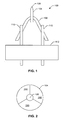
- FIG. 1 shows a cold field electron source embodying the present invention.
- FIG. 2 is an enlarged, top view of the emitter of the cold field emitter of FIG. 1 .
- FIG. 3 is a flow chart showing a preferred method of making and using the cold field electron source of FIG. 1 .
- FIG. 4 is a flow chart showing another preferred method of making and using the cold field electron source of FIG. 1 .
- FIG. 5 shows an electron instrument incorporating the cold field electron source of FIG. 1
- FIG. 1 shows a cold field electron source 100 embodying the invention.
- Cold field emitter 100 includes a filament 102 that supports and heats an emitter 104 having a tip 106 from which the electrons are emitted.
- Tip 106 has as small a radius as can be practically constructed, preferably less than 500 nm, more preferably less than 200 nm, and most preferably less than, or about, 100 nm.
- a heating current can be supplied to filament 102 through electrodes 110 that penetrate a base 112.
- Emitter 104 is heated as explained below as part of its preparation for operation, but is not typically heated during operation.
- Emitter 104 preferably comprises a base material of a single crystal of a metal oriented typically with the ⁇ 111>, ⁇ 110>, or ⁇ 310> crystal direction aligned along the emitter axis.
- Emitter 104 typically comprises tungsten, tantalum, rhenium, molybdenum, iridium, other similar metals or alloys of these metals.
- a preferred emitter base material is conductive, non-magnetic, has a low work function, and can be heated to a high temperature without significantly increasing the tip radius.
- the emitter base material is coated with a coating material.
- a preferred coating material does not readily adsorb background gases, such as oxygen, nitrogen, water vapor, and carbon containing gases.
- a preferred coating also has a low sputtering coefficient, that is, when hit by positive ions, relatively few atoms are released from the emitter.
- a preferred coating also increases the angular confinement of the electron beam. These desirable coating characteristics reduce short and long term current instabilities.
- a preferred coating may also reduce the work function of the emitter, although reducing the work function is not as important for a cold field emitter as for a Schottky emitter.
- the coating material can be grown on the emitter by causing a reaction between the material composing the emitter and another material introduced into the vacuum chamber, such as oxygen, nitrogen, or carbon.
- the coating can also be deposited onto the emitter.
- the coating could include, for example, compounds, such as oxide, nitrides and carbon compounds, of the emitter base material or of, for example, zirconium, titanium, hafnium, yttrium, niobium, vanadium, thorium, scandium, beryllium or lanthanum.
- the coating may include multiple species, such as a combination of carbon and oxygen on a tungsten emitter.
- a preferred combination of emitter base material and coating provides a cold field emitter that will operate at a low temperature, at a relatively high pressure compared to prior art cold field emitters, and provide greater stability.
- Preferred emitters of the present invention operate stably between about 73 K and 700 K, producing an output current of between 10 nA and 20 pA using extraction voltages of between about 900 V and 6000 V at pressures as high as 10 -8 Torr (1.3 x 10 -8 mbar) or higher.
- a preferred emitter can operate at a temperature of less than 700 K and a pressure greater than 10 -10 Torr (1.3 x 10 -10 mbar) for a period of 50 hours or greater with less than plus or minus 5%, or more preferably less than plus or minus 3%, change in beam current, with a beam current of greater than zero nA .
- Another preferred embodiment can operate at a temperature of less than 700 K and a pressure greater than 5 x 10 -10 Torr (7 x 10 -10 mbar) for a period of 50 hours or greater with less than plus or minus 5%, or more preferably less than plus or minus 3%, change in beam current, with a beam current of greater than zero nA.
- Another preferred emitter can operate at a temperature of less than 700 K and a pressure greater than 10 -9 Torr (1.3 x 10 -9 mbar) for a period of 24 hours with less than plus or minus 5%, or more preferably less than plus or minus 3%, change in beam current, with a beam current of greater than zero nA.
- Another preferred emitter can operate at a temperature of less than 700 K and a pressure greater than 5 x 10 -9 Torr (7 x 10 -9 mbar) for a period of 24 hours with less than plus or minus 5%, or more preferably less than plus or minus 3%, change in beam current, with a beam current of greater than zero nA.
- Yet another preferred emitter can operate at a temperature of less than 700 K and a pressure greater than 10 -8 Torr (1.3 x 10 -8 mbar) for a period of 24 hours with less than plus or minus 5% change in beam current, with a beam current of greater than zero nA.
- the emitter is typically operated without heating, and is therefore typically near room temperature during operation.
- the emitter can be heated to prevent adsorbates from sticking to the emitter surface should they land there, but the temperature to which the emitter is heated during operation is preferably sufficiently low to prevent such thermionic emission that would significantly increase the energy spread of the emitted electrons and to noticeably reduce the image resolution. That is, the temperature during operation is preferably less than about 700 K and more preferably less than about 350 K.
- emitter 104 comprises a single crystal tungsten wire having its longitudinal axis along a ⁇ 111> crystal orientation.
- Tip 106 ( Fig. 1 ) has a radius of curvature of preferably about 100 nm.
- the emitter 104 is at least partly coated with an oxide layer, the coating covering the emitting surface of the tip.
- FIG. 2 which is an enlarged top view of emitter 104, shows facets 250 in the emitter wire to expose three, high work function ⁇ 211 ⁇ crystal planes. Facets 250 form as a result of the oxidation process.
- the facets result in a high degree of confinement of the emission along the axial ⁇ 111> crystal direction.
- the facet surfaces can be characterized by their electron emission pattern and work function.
- the ⁇ 211 ⁇ crystal planes may be further faceted (i.e. built up) by heating in the presence of the electric field, to further confine the emission along the emitter axis.
- the oxide layer or other preferred coating has sufficient coverage so as to reduce the adsorption of residual gases on the emitting surface.
- the result is a relatively high brightness, cold field electron source that provides stable electron emission in vacuum levels readily achievable in many existing electron columns.
- an emitter of the present invention for longer than 500 hours at a pressure of 5x10 -10 Torr (7x10 -10 mbar) without a controlled feedback loop and with a relatively stable emission current of about 2 pA.
- the emission current may become unstable after an extended period of time. If the emission becomes unstable, thermal processing will restore the emitter to its original emission characteristics. For example, if the emitter coating was originally formed by exposing the emitter base material to a coating component in the form of a gas and then annealing the emitter, a "refresh" step may be performed by heating the emitter to the same temperature that was used in the original annealing step, and for the same duration.
- the refresh step preferably also entails heating the emitter to about 1400 K for about 60 seconds, with or without exposing the emitter to oxygen before or during the refresh annealing step.
- the preferred process for producing a particular coating can be determined empirically, for example, by varying the coating process and observing the emission and operating characteristics of the emitter after each variation. Emission characteristics are observed, for example, from field emission microscopy ("FEM”) images and from current versus voltage (“I/V”) curves. Operating characteristics refer to performance over a longer period of time and are observed by operating the emitter for an extended period of time under normal operating conditions.
- FEM field emission microscopy
- I/V current versus voltage
- a tungsten emitter is first cleaned by heating it briefly to a high temperature of about 2,200 K. After allowing the emitter to return to a temperature of between 300K and 1800K, it is then briefly exposed to oxygen to chemisorb oxygen or other coating components onto the emitter surface, and the emitter is then annealed for a first period of time, for example, 60 seconds, at a first temperature, for example, 700 K.
- anneal is used herein to mean heating the emitter to produce the desired coating. A FEM image is observed and I/V curves are plotted.
- the process is repeated, that is, the tungsten needle is cleaned again by briefly heating to a high temperature, exposed to oxygen, and heated again for the first time period at the first temperature.
- the emission characteristics are observed again. If desirable emission characteristics cannot be repeatedly achieved, the heating time and temperature are probably unsuitable for the materials selected.
- the emitter preparation process is then varied by varying the time and temperature until desirable emission characteristics are repeatedly achieved. For example, the emitter may be annealed at 800 K or 900 K after exposure to oxygen. After a process is found to repeatedly provide favorable emission characteristics, the operating characteristics of the emitter are observed by operating the emitter for an extended period of time. If the emitter exhibits suitable operating characteristics, then the coating process can be used to produce additional emitters.
- the solid angle of emission can be further confined by building up facets by applying temperature and high field simultaneously. This is more commonly referred to as a built-up emitter.
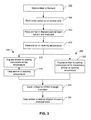
- FIG. 3 is a flow chart showing a preferred method of making a typical inventive cold field emitter such as the one shown in FIGS. 1 and 2 .
- a single crystal wire is welded to a filament 102, which has been previously welded to electrodes 110, which extend through base 112.
- the single crystal wire is formed into an emitter by forming a very narrow point, that is, a very small radius tip on the end of the wire.
- a single crystal tungsten wire, oriented with its axis in the ⁇ 111> crystal direction can be electrochemically etched, preferably using a direct current etching method, to form a radius of preferably less than 200 nm.
- the tip can also be formed using an alternating current etch method of using a loop method or emitter pull method, as taught in A. J. Melmed, "The Art And Science And Other Aspects Of Making Sharp Tips," Journal of Vacuum Science & Technology B: Microelectronics and Nanometer Structures, Vol. 9, Issue 2, pp. 601-608 (1991) .
- the relative position of the loop to the emitter is adjusted, or the emitter is pulled from the etching solution as required during the etching to achieve a radius of preferably less than 200 nm.
- the emitter is placed in a charged particle beam system and the system is evacuated, preferably to a pressure of less than 10 -8 Torr (1.3 x 10 -8 mbar) and more preferably to a pressure of about 5 x 10 -10 Torr (7 x 10 -10 mbar).
- the emitter is heated briefly, that is, for about 10 seconds, to about 2,200 K, to remove any contamination or adsorbed gas molecules from the tip. The cleanliness of the tip can be verified by observing an FEM image and by plotting an I/V curve for the emitter.
- a coating is formed at least on the emitter tip by reacting a coating component with the emitter.
- oxygen can be adsorbed onto a tungsten emitter tip and reacted with the tungsten to form an oxide of tungsten.
- the adsorption and reaction can be performed in separate steps, such as adsorbing the coating component onto the emitter at room temperature (step 316) and then heating the emitter to react the coating component with the emitter (step 318).
- the emitter is preferably heated to a temperature of greater than about 900 K and less than 1,800 K and more preferably to between about 1,000 K and about 1,200 K. The temperature should be sufficiently high to induce the reaction, yet not so high that the reaction product dissipates from the emitter.
- a tungsten emitter may be heated to about 1200 K for about 60 seconds to react adsorbed oxygen to form an oxide.
- the coating may be formed in a single step, as shown in step 322, by maintaining the emitter at a sufficiently elevated temperature to induce the reaction while introducing the coating component.
- oxygen for example may be leaked in to the vacuum chamber to a partial pressure of about 10 -6 Torr (1.3 x 10 -6 mbar) for about 3 minutes. The oxygen is then removed from the vacuum chamber by a vacuum pump.
- step 316 the adsorption of oxygen at room temperature forms a chemisorbed layer.
- Heating in step 318 transforms the chemisorbed layer of oxygen into an oxidized layer. While two processes are described above for forming a coating, other methods are known for forming coatings, and the invention is not limited to the methods described above. After the coating is formed, by whatever process, the emitter is now ready to be used.
- the emitter is typically heated by running a current through the filament. Voltage is not typically applied to the emitter during the steps 318 and 322.
- an extraction voltage of, for example, about 2000 V is applied between the filament and an extraction electrode (not shown) to begin extracting electrons from the emitter for normal operation.
- the extraction voltage is preferably between 1000 V and 3000 V and more preferably between 1000 V and 2000 V. Skilled persons will understand that the operating voltage will vary with the tip radius and other factors, such as tip material, crystal orientations, coating properties, emitter-counter electrode region geometry, and the presence of tip contaminants.
- An emitter of the present invention can be used in any electron beam system, including microscopes and spectrometers, such as scanning electron microscopes, transmission electron microscopes, scanning transmission electron microscope, Auger electron spectrometers, electron energy loss spectrometer, energy dispersive spectrometers, etc.
- the emitter tip may become contaminated by residual gases.
- the emitter is heated to clean the tip and restore the original emission characteristics.
- the emitter may be heated to the same temperature as was used in the initial annealing step, step 318 or 322, for about 60 seconds or for the duration of the initial annealing step.
- the emitter may be exposed again to a coating component, such as oxygen, before step 330.
- FIG. 4 is a flow chart showing another embodiment of the invention which produces an emitter in which emission is confined to a relatively small area and provides a surface layer that reduces the adsorption of residual gases.
- a preferred method for forming such a structure includes providing a field emitter with a ⁇ 111> orientation in step 400 and then cleaning the emitter by heating to 1800 K for 10 to 15 sec in step 402.
- the emitter is exposed to a pure oxygen pressure of about 1x10 -6 torr (1.7 x10 -6 mbar) for several minutes at room temperature.
- the emitter is heated to 1600 K for 30 to 60 sec.
- Performing steps 400 to 406 will produce an emitted having emission confined to a small solid angle centered on the axis of the emitter.
- Adsorbing oxygen on a tungsten (111) planar surface and heating it to an elevated temperature causes an array of 3-sided pyramids to form with ⁇ 112 ⁇ planes making up the sides of the pyramid. These pyramids grow because of the lower surface free energy of the ⁇ 112 ⁇ planes; upon heating to allow for surface mobility, the latter planes grow at the expense of the (111) plane.
- the ⁇ 112 ⁇ planes form a thin WO x oxide layer (x is unknown). The oxide layer will reduce the adsorption of residual gases on the emitter surface and improve emission stability at room temperature. Heating to a sufficiently higher temperatures, however, removes the WO x layer and restores the planar (111) surface.
- the emission can be further confined to a smaller solid angle by heating in optional step 408 the emitter in the presence of a field sufficient to obtain a few microamps of total current at a temperature of 1200 to 1600 K.
- the process by which this occurs is a faceting of the three ⁇ 112 ⁇ planes surrounding the axial (111) plane.
- the emitter can then be operated in step 410 stably at room temperature or at some elevated temperature provided the vacuum level is sufficiently low. If the emission becomes unstable, stable emission can be obtained in step 412 by re-heating the emitter at 1200 to 1400 K for several seconds.
- FIG. 4 provides an example with specific times and temperatures, but the invention is not limited to the processing parameters described in connection with FIG. 4 . A person of skill in the art can use the example of FIG. 4 to create other processes which use different times and temperatures, but are within the scope of the present invention.
- FIG. 5 shows a block diagram of an electron beam system 502, such as a scanning electron microscope, that incorporates a cold field electron source 100 of the present invention.
- Cold field electron source 504 is maintained within a vacuum chamber 506 that also includes an electron column 508, a secondary particle detector 510, and a specimen 512 on a stage 514.
- Controller 520 controls the components in the system 502 to direct an electron beam toward specimen 512 and to display an image of the work piece on a display 522 using secondary particles detected by detector 510.
- Electron beam system 502 is provided by way of example, and cold emitters in accordance with the invention are not limited in their application to the configuration shown.
- Embodiments of the present invention can increase the resolution of the electron microscope by providing a source that is bright and has a low energy spread. Embodiments can operate reliably at a pressure greater than that in which a prior art cold field emitter can operate reliably. Embodiments can also provide improved stability when operated at pressures similar to those used for conventional cold field emitters. Embodiments can also provide various analytical capabilities such as electron energy loss spectroscopy. Some embodiments of cold field emitters of the present invention can operate at vacuum levels that are typical for Schottky emitters. Emitters of the present invention can be used in almost any application in which electron emitters are required and are used not only in electron beam systems, but in dual beam or other multiple beam systems.
- emitters of the present invention can obviously also be operated under the more ideal conditions that were required by prior art cold field emitters. That is, embodiments of the invention have certain capabilities, but the invention still covers those embodiments even when those capabilities are not being utilized. Embodiments of the invention provide an angular electron emission that is sufficient for typically electron beam applications.
Claims (24)
- Source d'électrons de champ froid (100), comportant :une embase (112) ;deux électrodes (110) s'étendant à travers l'embase ;un filament (102) relié aux deux électrodes ; etun émetteur métallique (104) fixé au filament, l'émetteur métallique possédant une pointe d'émetteur (106) sur une extrémité ;dans laquellel'émetteur métallique est un émetteur monocristallin orienté selon une orientation <111>, une orientation <110> ou une orientation <310>, et ;l'émetteur métallique est recouvert par un revêtement sur la pointe d'émetteur d'un second matériau combiné chimiquement avec le matériau métallique de la pointe.
- Source d'électrons de champ froid selon la revendication 1, dans laquelle l'émetteur métallique (104) comporte du tungstène et le revêtement sur la pointe d'émetteur (106) comporte un composé d'azote et de tungstène ou un composé d'oxygène et de tungstène.
- Source d'électrons de champ froid selon les revendications 1 ou 2, dans laquelle la pointe d'émetteur (106) comporte des côtés comprenant des plans cristallins qui réduisent l'émission à distance de l'extrémité de la pointe d'émetteur, concentrant ainsi l'émission à la pointe.
- Source d'électrons de champ froid selon l'une quelconque des revendications précédentes, dans laquelle le revêtement réduit l'adsorption des gaz résiduels sur la pointe d'émetteur.
- Source d'électrons de champ froid selon l'une quelconque des revendications précédentes, dans laquelle l'émetteur métallique (104) est un émetteur en tungstène monocristallin possédant un axe longitudinal orienté dans la direction cristalline <111> et dans laquelle la pointe comprend un réseau de pyramides trilatérales, chaque côté de la pyramide comprenant un plan {112}.
- Source d'électrons de champ froid selon la revendication 5, dans laquelle les côtés de la pyramide comprennent une couche d'oxyde qui réduit l'adsorption des gaz résiduels et améliore la stabilité d'émission à température ambiante.
- Source d'électrons de champ froid selon l'une quelconque des revendications précédentes, dans laquelle la pointe d'émetteur (106) présente un rayon inférieur à 300 nm.
- Source d'électrons de champ froid selon l'une quelconque des revendications précédentes, dans laquelle l'émetteur recouvert peut fonctionner à une température à laquelle une émission thermo-ionique ne contribue pas de façon significative à la dispersion d'énergie entre les électrons émis et à une pression de 1,3 x 10⁻⁸ mbar pendant une période de 24 heures avec un changement inférieur de ±5% dans le courant de faisceau sans une boucle de contrôle à rétroaction externe, avec un courant de faisceau supérieur à zéro nA.
- Source d'électrons de champ froid selon l'une quelconque des revendications 1 à 7, dans laquelle l'émetteur recouvert peut fonctionner à une température inférieure à 700 K et à une pression de 1,3 x 10⁻⁹ mbar pendant une période de 24 heures avec un changement inférieur de ±5% dans le courant de faisceau sans une boucle de contrôle à rétroaction externe, avec un courant de faisceau supérieur à zéro nA.
- Source d'électrons de champ froid selon l'une quelconque des revendications précédentes, dans laquelle le revêtement du second matériau comprend une couverture inférieure à une monocouche.
- Instrument électronique (402) possédant une source d'électrons de champ froid selon l'une quelconque des revendications précédentes, l'instrument électronique comprenant un microscope électronique à balayage, un microscope électronique par transmission, un microscope électronique à balayage par transmission, un spectromètre Auger, ou un spectromètre de pertes d'énergie des électrons, ou un spectromètre à dispersion d'énergie dispersive ou un instrument quelconque avec une capacité de concentration électronique.
- Utilisation d'un émetteur de champ froid (100), l'émetteur de champ froid comportant :une embase (112) ;des électrodes multiples (110) s'étendant à travers l'embase ;un filament (102) relié à deux des électrodes ;un émetteur (104) fixé au filament, l'émetteur possédant à une extrémité une pointe d'émetteur monocristalline (106) en un matériau de pointe d'émetteur ;une couche d'un matériau de revêtement sur la pointe d'émetteur, l'utilisation comportant :l'application d'une tension d'extraction près de la pointe d'émetteur pour extraire les électrons tout en maintenant la pointe d'émetteur à une température telle qu'aucune émission thermo-ionique significative ne se produit,dans laquellela pointe d'émetteur monocristalline est orientée selon la direction <111>, <110> ou <310> ;la couche d'un matériau de revêtement comprend une combinaison chimique du matériau dont est constituée la pointe d'émetteur et d'un autre matériau.
- Utilisation selon la revendication 12, dans laquelle la couche d'un matériau de revêtement sur la pointe d'émetteur est formée par un processus comprenant l'exposition d'une pointe d'émetteur en tungstène (106) à l'oxygène ou à l'azote et ensuite en chauffant la pointe suffisamment pour faire réagir le tungstène avec l'oxygène ou l'azote.
- Utilisation selon la revendication 12, dans laquelle la pointe d'émetteur monocristalline possède un axe longitudinal orienté dans la direction cristalline <111> et dans laquelle la couche d'un matériau de revêtement est formée par un processus comprenant le chauffage de la pointe d'émetteur (106) à une température suffisante pour former un réseau de pyramides définies par des plans {112}.
- Utilisation selon la revendication 12, dans laquelle la couche d'un matériau de revêtement sur la pointe d'émetteur est formée par un processus comprenant la délivrance d'un oxyde ou d'un nitrure du matériau composant l'émetteur.
- Utilisation selon la revendication 12, dans laquelle la couche d'un matériau de revêtement sur la pointe d'émetteur possède une couverture inférieure à une monocouche.
- Utilisation selon la revendication 12, comportant en outre le chauffage de l'émetteur tout en extrayant les électrons pour ainsi confiner l'émission à la pointe de l'émetteur avant de le faire fonctionner.
- Utilisation selon la revendication 12, dans laquelle l'application d'une tension d'extraction pour faire fonctionner l'émetteur à une température inférieure à 700 K à une pression supérieure à 7 x 10⁻⁹ mbar pendant plus de 50 heures avec un changement inférieur à ±5% dans un courant de faisceau sans une boucle de contrôle à rétroaction externe, avec un courant de faisceau supérieur à zéro nA.
- Utilisation selon la revendication 12, dans laquelle l'application d'une tension d'extraction comprend l'application d'une tension d'extraction dans une chambre à vide à une pression égale à ou supérieure à 1,3 x 10⁻⁹ mbar pour extraire les électrons continûment pendant une période supérieure à 24 heures avec une variation du courant de faisceau inférieure à 5% sans une boucle de contrôle à rétroaction externe, avec un courant de faisceau supérieur à zéro nA.
- Processus de fabrication d'un émetteur de champ froid, comprenant :la mise en place d'un fil possédant une partie s'effilant vers une pointe ;l'exposition du fil au gaz à une faible pression pour adsorber les molécules de gaz sur le fil ;dans lequelle fil est un monocristal aligné selon une orientation <111>, une orientation <110> ou une orientation <310> ; etle chauffage du fil après exposition du fil à un gaz à une faible pression à une température suffisante pour faire réagir les molécules de gaz adsorbées avec le fil pour former un revêtement d'un second matériau chimiquement combiné au matériau du fil qui améliore la stabilité de l'émission à de faibles températures.
- Processus selon la revendication 20, dans lequel le chauffage du fil après exposition du fil à un gaz à une faible pression à une température suffisante pour faire réagir les molécules de gaz adsorbées avec le fil comprend une formation de plans de faible émission de sorte que l'émission provenant du fil est concentrée à la pointe du fil.
- Processus selon la revendication 20, comportant en outre le chauffage de l'émetteur au-delà de la température de fonctionnement tout en extrayant les électrons pour ainsi confiner l'émission à la pointe de l'émetteur après chauffage du fil après exposition du fil à un gaz à une faible pression et avant le fonctionnement de l'émetteur.
- Processus selon la revendication 20, dans lequel :la mise en place d'un fil comporte la mise en place d'un fil en tungstène ;l'exposition du fil à un gaz à une faible pression comprend l'exposition du fil à l'oxygène à une pression partielle inférieure à 1,3 x 10⁻⁴ mbar ; etle chauffage du fil comporte le chauffage du fil à plus de 1000 K.
- Processus selon la revendication 23, dans lequel la mise en place d'un fil comporte la mise en place d'un fil en tungstène comportant un fil en tungstène monocristallin possédant un rayon de pointe inférieur à 400 nm et un axe longitudinal orienté dans la direction cristalline <111>.
Applications Claiming Priority (2)
| Application Number | Priority Date | Filing Date | Title |
|---|---|---|---|
| US89736907P | 2007-01-24 | 2007-01-24 | |
| US11/900,956 US7888654B2 (en) | 2007-01-24 | 2007-09-14 | Cold field emitter |
Publications (3)
| Publication Number | Publication Date |
|---|---|
| EP1950786A2 EP1950786A2 (fr) | 2008-07-30 |
| EP1950786A3 EP1950786A3 (fr) | 2009-03-25 |
| EP1950786B1 true EP1950786B1 (fr) | 2011-03-09 |
Family
ID=39301320
Family Applications (1)
| Application Number | Title | Priority Date | Filing Date |
|---|---|---|---|
| EP08100824A Active EP1950786B1 (fr) | 2007-01-24 | 2008-01-23 | Émetteur de champ froid |
Country Status (5)
| Country | Link |
|---|---|
| US (2) | US7888654B2 (fr) |
| EP (1) | EP1950786B1 (fr) |
| JP (1) | JP5301168B2 (fr) |
| AT (1) | ATE501520T1 (fr) |
| DE (1) | DE602008005354D1 (fr) |
Families Citing this family (26)
| Publication number | Priority date | Publication date | Assignee | Title |
|---|---|---|---|---|
| US7888654B2 (en) * | 2007-01-24 | 2011-02-15 | Fei Company | Cold field emitter |
| DE112009001537B8 (de) * | 2008-06-20 | 2019-01-24 | Hitachi High-Technologies Corporation | Vorrichtung mit geladenem Teilchenstrahl und Verfahren zum Steuern der Vorrichtung |
| DE102008049654A1 (de) * | 2008-09-30 | 2010-04-08 | Carl Zeiss Nts Gmbh | Elektronenstrahlquelle und Verfahren zur Herstellung derselben |
| WO2010144267A1 (fr) * | 2009-06-12 | 2010-12-16 | Carl Zeiss Nts, Llc | Procédé et système de chauffage de l'extrémité de pointe d'une source de particules chargées |
| JP2011076753A (ja) * | 2009-09-29 | 2011-04-14 | Denki Kagaku Kogyo Kk | 電子源及び電子機器 |
| JP5455700B2 (ja) * | 2010-02-18 | 2014-03-26 | 株式会社日立ハイテクノロジーズ | 電界放出電子銃及びその制御方法 |
| JP5363413B2 (ja) * | 2010-05-10 | 2013-12-11 | 電気化学工業株式会社 | 電子源 |
| US8847173B2 (en) * | 2010-08-06 | 2014-09-30 | Hitachi High-Technologies Corporation | Gas field ion source and method for using same, ion beam device, and emitter tip and method for manufacturing same |
| KR101027397B1 (ko) | 2010-08-27 | 2011-04-11 | 손호섭 | 전기 및 전자 소자의 검사를 위한 초소형 전자칼럼용 텅스텐 cfe의 제조 방법 |
| US8736170B1 (en) | 2011-02-22 | 2014-05-27 | Fei Company | Stable cold field emission electron source |
| US8536773B2 (en) | 2011-03-30 | 2013-09-17 | Carl Zeiss Microscopy Gmbh | Electron beam source and method of manufacturing the same |
| CN102629538B (zh) * | 2012-04-13 | 2014-03-19 | 吴江炀晟阴极材料有限公司 | 具有低逸出功和高化学稳定性的电极材料 |
| US10790403B1 (en) | 2013-03-14 | 2020-09-29 | nVizix LLC | Microfabricated vacuum photodiode arrays for solar power |
| US10249471B2 (en) | 2014-12-26 | 2019-04-02 | Hitachi High-Technologies Corporation | Composite charged particle beam apparatus and control method thereof |
| US9984846B2 (en) | 2016-06-30 | 2018-05-29 | Kla-Tencor Corporation | High brightness boron-containing electron beam emitters for use in a vacuum environment |
| KR20190032592A (ko) * | 2016-08-08 | 2019-03-27 | 에이에스엠엘 네델란즈 비.브이. | 전자 이미터 및 이의 제작 방법 |
| US9847208B1 (en) * | 2016-08-10 | 2017-12-19 | ICT Integrated Circuit Testing Gesellschaft für Halbleiterprüftechnik mbH | Electron beam device, cold field emitter, and method for regeneration of a cold field emitter |
| US10410827B2 (en) * | 2017-05-03 | 2019-09-10 | Fei Company | Gun lens design in a charged particle microscope |
| WO2018217167A1 (fr) | 2017-05-25 | 2018-11-29 | National University Of Singapore | Structure de cathode pour émission d'électrons de champ froid et son procédé de fabrication |
| FR3074955B1 (fr) * | 2017-12-07 | 2021-01-08 | Thales Sa | Source d'electrons a commande optique amelioree |
| CN109936906B (zh) * | 2017-12-15 | 2024-03-08 | 中国科学院大连化学物理研究所 | 光阴极电子枪射频同步慢飘抑制装置 |
| CN111048373B (zh) * | 2018-10-12 | 2021-04-27 | 中国电子科技集团公司第三十八研究所 | 一种电子源再生方法 |
| US11417492B2 (en) | 2019-09-26 | 2022-08-16 | Kla Corporation | Light modulated electron source |
| US11823862B2 (en) * | 2021-12-29 | 2023-11-21 | Nuflare Technology, Inc. | Method and apparatus for usable beam current and brightness in Schottky thermal field emission (TFE) |
| US11651924B1 (en) | 2022-06-22 | 2023-05-16 | Fei Company | Method of producing microrods for electron emitters, and associated microrods and electron emitters |
| US11848169B1 (en) * | 2023-01-21 | 2023-12-19 | Dazhi Chen | Field-emission type electron source and charged particle beam device using the same |
Family Cites Families (18)
| Publication number | Priority date | Publication date | Assignee | Title |
|---|---|---|---|---|
| US3817592A (en) | 1972-09-29 | 1974-06-18 | Linfield Res Inst | Method for reproducibly fabricating and using stable thermal-field emission cathodes |
| GB1477458A (en) | 1974-10-28 | 1977-06-22 | Shah J | Specimen stages for electron beam instruments |
| JPS5661733A (en) | 1979-10-24 | 1981-05-27 | Hitachi Ltd | Field emission cathode and its manufacture |
| JPS5971232A (ja) * | 1982-10-14 | 1984-04-21 | Natl Inst For Res In Inorg Mater | 表面酸化型炭化物フィールドエミッターの製造法 |
| JPS61190830A (ja) * | 1984-12-27 | 1986-08-25 | Natl Inst For Res In Inorg Mater | チタンオキシカーバイドエミッターの製造方法 |
| DE3887891T2 (de) * | 1988-11-01 | 1994-08-11 | Ibm | Niederspannungsquelle für schmale Elektronen-/Ionenstrahlenbündel. |
| US5449968A (en) | 1992-06-24 | 1995-09-12 | Denki Kagaku Kogyo Kabushiki Kaisha | Thermal field emission cathode |
| JPH08250054A (ja) * | 1995-03-14 | 1996-09-27 | Hitachi Ltd | 拡散補給型電子線源およびそれを用いた電子線装置 |
| US6680562B1 (en) | 1999-08-20 | 2004-01-20 | Fei Company | Schottky emitter having extended life |
| US6771013B2 (en) | 2000-10-17 | 2004-08-03 | Fei Company | Low power schottky emitter |
| JP2003100244A (ja) * | 2001-09-26 | 2003-04-04 | Jeol Ltd | 電子ビーム源 |
| US6798126B2 (en) | 2002-05-03 | 2004-09-28 | Fei Company | High angular intensity Schottky electron point source |
| JP4792404B2 (ja) * | 2005-01-14 | 2011-10-12 | 電気化学工業株式会社 | 電子源の製造方法 |
| WO2006135092A1 (fr) * | 2005-06-17 | 2006-12-21 | Sumitomo Electric Industries, Ltd. | Cathode d'émission d'électrons en diamant, source d'émission d'électrons, microscope électronique et dispositif d'exposition à faisceau électronique |
| EP1760761B1 (fr) * | 2005-09-05 | 2017-10-18 | ICT, Integrated Circuit Testing Gesellschaft für Halbleiterprüftechnik mbH | Emetteur de faisceau à particules chargées et procédé de fonctionnement d'un émetteur de faisceau à particules chargées |
| EP1777730B1 (fr) * | 2005-10-19 | 2018-05-30 | ICT Integrated Circuit Testing Gesellschaft für Halbleiterprüftechnik mbH | Dispositif et méthode de compensation de la vibration d'une pointe d'un émetteur |
| US7544523B2 (en) | 2005-12-23 | 2009-06-09 | Fei Company | Method of fabricating nanodevices |
| US7888654B2 (en) * | 2007-01-24 | 2011-02-15 | Fei Company | Cold field emitter |
-
2007
- 2007-09-14 US US11/900,956 patent/US7888654B2/en active Active
-
2008
- 2008-01-21 JP JP2008010227A patent/JP5301168B2/ja active Active
- 2008-01-23 AT AT08100824T patent/ATE501520T1/de not_active IP Right Cessation
- 2008-01-23 DE DE602008005354T patent/DE602008005354D1/de active Active
- 2008-01-23 EP EP08100824A patent/EP1950786B1/fr active Active
-
2011
- 2011-01-10 US US12/987,338 patent/US8217565B2/en active Active
Also Published As
| Publication number | Publication date |
|---|---|
| JP5301168B2 (ja) | 2013-09-25 |
| US8217565B2 (en) | 2012-07-10 |
| US7888654B2 (en) | 2011-02-15 |
| EP1950786A3 (fr) | 2009-03-25 |
| DE602008005354D1 (de) | 2011-04-21 |
| US20080174225A1 (en) | 2008-07-24 |
| ATE501520T1 (de) | 2011-03-15 |
| EP1950786A2 (fr) | 2008-07-30 |
| US20110101238A1 (en) | 2011-05-05 |
| JP2008181876A (ja) | 2008-08-07 |
Similar Documents
| Publication | Publication Date | Title |
|---|---|---|
| EP1950786B1 (fr) | Émetteur de champ froid | |
| US7777404B1 (en) | Field emission type electron gun comprising single fibrous carbon electron emitter and operating method for the same | |
| US7737414B2 (en) | Atomically sharp iridium tip | |
| US9984846B2 (en) | High brightness boron-containing electron beam emitters for use in a vacuum environment | |
| US7151268B2 (en) | Field emission gun and electron beam instruments | |
| EP1359599B1 (fr) | Source électronique ponctuelle à effet Schottky avec haute intensité angulaire | |
| US20140077684A1 (en) | Particle sources and methods for manufacturing the same | |
| EP2546862B1 (fr) | Source de particules et appareil utilisant la source de particules | |
| CN109804450B (zh) | 电子束装置 | |
| EP2575158B1 (fr) | Procédé de fabrication d'une source de particules | |
| US7828622B1 (en) | Sharpening metal carbide emitters | |
| TW202013410A (zh) | 用於具有一擴散障壁之電子發射器之金屬保護層 | |
| JP4292108B2 (ja) | 電子源及びその製造方法 | |
| CN111048383B (zh) | 电子源和电子枪 | |
| EP1596418B1 (fr) | Canon à electrons | |
| CN111048382B (zh) | 电子源制造方法 | |
| EP3996126A1 (fr) | Émetteur, canon à électrons l'utilisant, dispositif électronique l'utilisant et son procédé de production | |
| US11984294B2 (en) | Emitter, electron gun in which same is used, electronic device in which same is used, and method for manufacturing same | |
| JP2010272504A (ja) | 炭素系材料からなる電子源及びその製造方法 | |
| Spindt et al. | Spindt field emitter arrays | |
| Chen et al. | Field emission studies of tungsten-coated silicon-based field emitters | |
| Schmidt et al. | Nanoemitter: ultra-high-resolution electron source for CD metrology |
Legal Events
| Date | Code | Title | Description |
|---|---|---|---|
| PUAI | Public reference made under article 153(3) epc to a published international application that has entered the european phase |
Free format text: ORIGINAL CODE: 0009012 |
|
| AK | Designated contracting states |
Kind code of ref document: A2 Designated state(s): AT BE BG CH CY CZ DE DK EE ES FI FR GB GR HR HU IE IS IT LI LT LU LV MC MT NL NO PL PT RO SE SI SK TR |
|
| AX | Request for extension of the european patent |
Extension state: AL BA MK RS |
|
| PUAL | Search report despatched |
Free format text: ORIGINAL CODE: 0009013 |
|
| AK | Designated contracting states |
Kind code of ref document: A3 Designated state(s): AT BE BG CH CY CZ DE DK EE ES FI FR GB GR HR HU IE IS IT LI LT LU LV MC MT NL NO PL PT RO SE SI SK TR |
|
| AX | Request for extension of the european patent |
Extension state: AL BA MK RS |
|
| RIC1 | Information provided on ipc code assigned before grant |
Ipc: H01J 1/304 20060101ALI20090219BHEP Ipc: H01J 9/02 20060101ALI20090219BHEP Ipc: H01J 37/073 20060101AFI20090219BHEP |
|
| 17P | Request for examination filed |
Effective date: 20090403 |
|
| 17Q | First examination report despatched |
Effective date: 20090512 |
|
| AKX | Designation fees paid |
Designated state(s): AT BE BG CH CY CZ DE DK EE ES FI FR GB GR HR HU IE IS IT LI LT LU LV MC MT NL NO PL PT RO SE SI SK TR |
|
| GRAP | Despatch of communication of intention to grant a patent |
Free format text: ORIGINAL CODE: EPIDOSNIGR1 |
|
| GRAS | Grant fee paid |
Free format text: ORIGINAL CODE: EPIDOSNIGR3 |
|
| GRAA | (expected) grant |
Free format text: ORIGINAL CODE: 0009210 |
|
| AK | Designated contracting states |
Kind code of ref document: B1 Designated state(s): AT BE BG CH CY CZ DE DK EE ES FI FR GB GR HR HU IE IS IT LI LT LU LV MC MT NL NO PL PT RO SE SI SK TR |
|
| REG | Reference to a national code |
Ref country code: GB Ref legal event code: FG4D |
|
| REG | Reference to a national code |
Ref country code: CH Ref legal event code: EP |
|
| REG | Reference to a national code |
Ref country code: IE Ref legal event code: FG4D |
|
| REF | Corresponds to: |
Ref document number: 602008005354 Country of ref document: DE Date of ref document: 20110421 Kind code of ref document: P |
|
| REG | Reference to a national code |
Ref country code: DE Ref legal event code: R096 Ref document number: 602008005354 Country of ref document: DE Effective date: 20110421 |
|
| REG | Reference to a national code |
Ref country code: NL Ref legal event code: VDEP Effective date: 20110309 |
|
| PG25 | Lapsed in a contracting state [announced via postgrant information from national office to epo] |
Ref country code: HR Free format text: LAPSE BECAUSE OF FAILURE TO SUBMIT A TRANSLATION OF THE DESCRIPTION OR TO PAY THE FEE WITHIN THE PRESCRIBED TIME-LIMIT Effective date: 20110309 Ref country code: LV Free format text: LAPSE BECAUSE OF FAILURE TO SUBMIT A TRANSLATION OF THE DESCRIPTION OR TO PAY THE FEE WITHIN THE PRESCRIBED TIME-LIMIT Effective date: 20110309 Ref country code: ES Free format text: LAPSE BECAUSE OF FAILURE TO SUBMIT A TRANSLATION OF THE DESCRIPTION OR TO PAY THE FEE WITHIN THE PRESCRIBED TIME-LIMIT Effective date: 20110620 Ref country code: LT Free format text: LAPSE BECAUSE OF FAILURE TO SUBMIT A TRANSLATION OF THE DESCRIPTION OR TO PAY THE FEE WITHIN THE PRESCRIBED TIME-LIMIT Effective date: 20110309 Ref country code: GR Free format text: LAPSE BECAUSE OF FAILURE TO SUBMIT A TRANSLATION OF THE DESCRIPTION OR TO PAY THE FEE WITHIN THE PRESCRIBED TIME-LIMIT Effective date: 20110610 Ref country code: SE Free format text: LAPSE BECAUSE OF FAILURE TO SUBMIT A TRANSLATION OF THE DESCRIPTION OR TO PAY THE FEE WITHIN THE PRESCRIBED TIME-LIMIT Effective date: 20110309 Ref country code: NO Free format text: LAPSE BECAUSE OF FAILURE TO SUBMIT A TRANSLATION OF THE DESCRIPTION OR TO PAY THE FEE WITHIN THE PRESCRIBED TIME-LIMIT Effective date: 20110609 |
|
| LTIE | Lt: invalidation of european patent or patent extension |
Effective date: 20110309 |
|
| PG25 | Lapsed in a contracting state [announced via postgrant information from national office to epo] |
Ref country code: CY Free format text: LAPSE BECAUSE OF FAILURE TO SUBMIT A TRANSLATION OF THE DESCRIPTION OR TO PAY THE FEE WITHIN THE PRESCRIBED TIME-LIMIT Effective date: 20110309 Ref country code: FI Free format text: LAPSE BECAUSE OF FAILURE TO SUBMIT A TRANSLATION OF THE DESCRIPTION OR TO PAY THE FEE WITHIN THE PRESCRIBED TIME-LIMIT Effective date: 20110309 Ref country code: BG Free format text: LAPSE BECAUSE OF FAILURE TO SUBMIT A TRANSLATION OF THE DESCRIPTION OR TO PAY THE FEE WITHIN THE PRESCRIBED TIME-LIMIT Effective date: 20110609 Ref country code: NL Free format text: LAPSE BECAUSE OF FAILURE TO SUBMIT A TRANSLATION OF THE DESCRIPTION OR TO PAY THE FEE WITHIN THE PRESCRIBED TIME-LIMIT Effective date: 20110309 Ref country code: AT Free format text: LAPSE BECAUSE OF FAILURE TO SUBMIT A TRANSLATION OF THE DESCRIPTION OR TO PAY THE FEE WITHIN THE PRESCRIBED TIME-LIMIT Effective date: 20110309 Ref country code: SI Free format text: LAPSE BECAUSE OF FAILURE TO SUBMIT A TRANSLATION OF THE DESCRIPTION OR TO PAY THE FEE WITHIN THE PRESCRIBED TIME-LIMIT Effective date: 20110309 |
|
| PG25 | Lapsed in a contracting state [announced via postgrant information from national office to epo] |
Ref country code: BE Free format text: LAPSE BECAUSE OF FAILURE TO SUBMIT A TRANSLATION OF THE DESCRIPTION OR TO PAY THE FEE WITHIN THE PRESCRIBED TIME-LIMIT Effective date: 20110309 |
|
| PG25 | Lapsed in a contracting state [announced via postgrant information from national office to epo] |
Ref country code: PT Free format text: LAPSE BECAUSE OF FAILURE TO SUBMIT A TRANSLATION OF THE DESCRIPTION OR TO PAY THE FEE WITHIN THE PRESCRIBED TIME-LIMIT Effective date: 20110711 Ref country code: EE Free format text: LAPSE BECAUSE OF FAILURE TO SUBMIT A TRANSLATION OF THE DESCRIPTION OR TO PAY THE FEE WITHIN THE PRESCRIBED TIME-LIMIT Effective date: 20110309 |
|
| PG25 | Lapsed in a contracting state [announced via postgrant information from national office to epo] |
Ref country code: CZ Free format text: LAPSE BECAUSE OF FAILURE TO SUBMIT A TRANSLATION OF THE DESCRIPTION OR TO PAY THE FEE WITHIN THE PRESCRIBED TIME-LIMIT Effective date: 20110309 Ref country code: IS Free format text: LAPSE BECAUSE OF FAILURE TO SUBMIT A TRANSLATION OF THE DESCRIPTION OR TO PAY THE FEE WITHIN THE PRESCRIBED TIME-LIMIT Effective date: 20110709 Ref country code: RO Free format text: LAPSE BECAUSE OF FAILURE TO SUBMIT A TRANSLATION OF THE DESCRIPTION OR TO PAY THE FEE WITHIN THE PRESCRIBED TIME-LIMIT Effective date: 20110309 Ref country code: SK Free format text: LAPSE BECAUSE OF FAILURE TO SUBMIT A TRANSLATION OF THE DESCRIPTION OR TO PAY THE FEE WITHIN THE PRESCRIBED TIME-LIMIT Effective date: 20110309 |
|
| PLBE | No opposition filed within time limit |
Free format text: ORIGINAL CODE: 0009261 |
|
| STAA | Information on the status of an ep patent application or granted ep patent |
Free format text: STATUS: NO OPPOSITION FILED WITHIN TIME LIMIT |
|
| 26N | No opposition filed |
Effective date: 20111212 |
|
| PG25 | Lapsed in a contracting state [announced via postgrant information from national office to epo] |
Ref country code: DK Free format text: LAPSE BECAUSE OF FAILURE TO SUBMIT A TRANSLATION OF THE DESCRIPTION OR TO PAY THE FEE WITHIN THE PRESCRIBED TIME-LIMIT Effective date: 20110309 Ref country code: PL Free format text: LAPSE BECAUSE OF FAILURE TO SUBMIT A TRANSLATION OF THE DESCRIPTION OR TO PAY THE FEE WITHIN THE PRESCRIBED TIME-LIMIT Effective date: 20110309 |
|
| REG | Reference to a national code |
Ref country code: DE Ref legal event code: R097 Ref document number: 602008005354 Country of ref document: DE Effective date: 20111212 |
|
| PG25 | Lapsed in a contracting state [announced via postgrant information from national office to epo] |
Ref country code: IT Free format text: LAPSE BECAUSE OF FAILURE TO SUBMIT A TRANSLATION OF THE DESCRIPTION OR TO PAY THE FEE WITHIN THE PRESCRIBED TIME-LIMIT Effective date: 20110309 |
|
| PG25 | Lapsed in a contracting state [announced via postgrant information from national office to epo] |
Ref country code: MC Free format text: LAPSE BECAUSE OF NON-PAYMENT OF DUE FEES Effective date: 20120131 |
|
| REG | Reference to a national code |
Ref country code: CH Ref legal event code: PL |
|
| REG | Reference to a national code |
Ref country code: IE Ref legal event code: MM4A |
|
| PG25 | Lapsed in a contracting state [announced via postgrant information from national office to epo] |
Ref country code: CH Free format text: LAPSE BECAUSE OF NON-PAYMENT OF DUE FEES Effective date: 20120131 Ref country code: LI Free format text: LAPSE BECAUSE OF NON-PAYMENT OF DUE FEES Effective date: 20120131 |
|
| PG25 | Lapsed in a contracting state [announced via postgrant information from national office to epo] |
Ref country code: IE Free format text: LAPSE BECAUSE OF NON-PAYMENT OF DUE FEES Effective date: 20120123 |
|
| PG25 | Lapsed in a contracting state [announced via postgrant information from national office to epo] |
Ref country code: MT Free format text: LAPSE BECAUSE OF FAILURE TO SUBMIT A TRANSLATION OF THE DESCRIPTION OR TO PAY THE FEE WITHIN THE PRESCRIBED TIME-LIMIT Effective date: 20110309 |
|
| PG25 | Lapsed in a contracting state [announced via postgrant information from national office to epo] |
Ref country code: TR Free format text: LAPSE BECAUSE OF FAILURE TO SUBMIT A TRANSLATION OF THE DESCRIPTION OR TO PAY THE FEE WITHIN THE PRESCRIBED TIME-LIMIT Effective date: 20110309 |
|
| PG25 | Lapsed in a contracting state [announced via postgrant information from national office to epo] |
Ref country code: LU Free format text: LAPSE BECAUSE OF NON-PAYMENT OF DUE FEES Effective date: 20120123 |
|
| PG25 | Lapsed in a contracting state [announced via postgrant information from national office to epo] |
Ref country code: HU Free format text: LAPSE BECAUSE OF FAILURE TO SUBMIT A TRANSLATION OF THE DESCRIPTION OR TO PAY THE FEE WITHIN THE PRESCRIBED TIME-LIMIT Effective date: 20080123 |
|
| REG | Reference to a national code |
Ref country code: FR Ref legal event code: PLFP Year of fee payment: 9 |
|
| REG | Reference to a national code |
Ref country code: FR Ref legal event code: PLFP Year of fee payment: 10 |
|
| REG | Reference to a national code |
Ref country code: FR Ref legal event code: PLFP Year of fee payment: 11 |
|
| PGFP | Annual fee paid to national office [announced via postgrant information from national office to epo] |
Ref country code: FR Payment date: 20230125 Year of fee payment: 16 |
|
| PGFP | Annual fee paid to national office [announced via postgrant information from national office to epo] |
Ref country code: DE Payment date: 20240109 Year of fee payment: 17 Ref country code: GB Payment date: 20240117 Year of fee payment: 17 |