EP1945563B1 - In der mikrosystemtechnik einsetzbares bauelement sowie lötverfahren zum verbinden entsprechender wafer- bzw. bauelement-teile - Google Patents
In der mikrosystemtechnik einsetzbares bauelement sowie lötverfahren zum verbinden entsprechender wafer- bzw. bauelement-teile Download PDFInfo
- Publication number
- EP1945563B1 EP1945563B1 EP06819339.0A EP06819339A EP1945563B1 EP 1945563 B1 EP1945563 B1 EP 1945563B1 EP 06819339 A EP06819339 A EP 06819339A EP 1945563 B1 EP1945563 B1 EP 1945563B1
- Authority
- EP
- European Patent Office
- Prior art keywords
- component
- annular
- wafer
- region
- cover
- Prior art date
- Legal status (The legal status is an assumption and is not a legal conclusion. Google has not performed a legal analysis and makes no representation as to the accuracy of the status listed.)
- Active
Links
Images

Classifications
-
- B—PERFORMING OPERATIONS; TRANSPORTING
- B81—MICROSTRUCTURAL TECHNOLOGY
- B81C—PROCESSES OR APPARATUS SPECIALLY ADAPTED FOR THE MANUFACTURE OR TREATMENT OF MICROSTRUCTURAL DEVICES OR SYSTEMS
- B81C99/00—Subject matter not provided for in other groups of this subclass
-
- B—PERFORMING OPERATIONS; TRANSPORTING
- B81—MICROSTRUCTURAL TECHNOLOGY
- B81C—PROCESSES OR APPARATUS SPECIALLY ADAPTED FOR THE MANUFACTURE OR TREATMENT OF MICROSTRUCTURAL DEVICES OR SYSTEMS
- B81C1/00—Manufacture or treatment of devices or systems in or on a substrate
- B81C1/00015—Manufacture or treatment of devices or systems in or on a substrate for manufacturing microsystems
- B81C1/00261—Processes for packaging MEMS devices
- B81C1/00269—Bonding of solid lids or wafers to the substrate
-
- B—PERFORMING OPERATIONS; TRANSPORTING
- B23—MACHINE TOOLS; METAL-WORKING NOT OTHERWISE PROVIDED FOR
- B23K—SOLDERING OR UNSOLDERING; WELDING; CLADDING OR PLATING BY SOLDERING OR WELDING; CUTTING BY APPLYING HEAT LOCALLY, e.g. FLAME CUTTING; WORKING BY LASER BEAM
- B23K1/00—Soldering, e.g. brazing, or unsoldering
-
- H—ELECTRICITY
- H05—ELECTRIC TECHNIQUES NOT OTHERWISE PROVIDED FOR
- H05K—PRINTED CIRCUITS; CASINGS OR CONSTRUCTIONAL DETAILS OF ELECTRIC APPARATUS; MANUFACTURE OF ASSEMBLAGES OF ELECTRICAL COMPONENTS
- H05K3/00—Apparatus or processes for manufacturing printed circuits
- H05K3/30—Assembling printed circuits with electric components, e.g. with resistor
- H05K3/32—Assembling printed circuits with electric components, e.g. with resistor electrically connecting electric components or wires to printed circuits
- H05K3/34—Assembling printed circuits with electric components, e.g. with resistor electrically connecting electric components or wires to printed circuits by soldering
-
- Y—GENERAL TAGGING OF NEW TECHNOLOGICAL DEVELOPMENTS; GENERAL TAGGING OF CROSS-SECTIONAL TECHNOLOGIES SPANNING OVER SEVERAL SECTIONS OF THE IPC; TECHNICAL SUBJECTS COVERED BY FORMER USPC CROSS-REFERENCE ART COLLECTIONS [XRACs] AND DIGESTS
- Y10—TECHNICAL SUBJECTS COVERED BY FORMER USPC
- Y10T—TECHNICAL SUBJECTS COVERED BY FORMER US CLASSIFICATION
- Y10T428/00—Stock material or miscellaneous articles
- Y10T428/23—Sheet including cover or casing
Definitions
- the present invention is directed to articles and methods for controlling wetting propagation of excess molten metal in the encapsulation of microcomponents, particularly at the wafer level.
- microsystem components are preferably manufactured using semiconductor technology manufacturing methods. As a result, many components can be produced at the same time cost. These components are, however, due to their very small dimensions, extremely sensitive and must be protected during operation or even during production against external influences. This is accomplished by hermetically sealing these components with protective caps.
- lid wafer a separate lid chip (lid wafer) is glued to the wafers containing the active structures or applied by other joining methods and so the elements are hermetically sealed.
- methods that encapsulate the MST wafer at the wafer level are also known for some time.
- a wafer which may consist for example of glass or silicon and generally contains one or more cavities for receiving the active component parts, connected by means of an anodic connection or by using glass solders. Less widespread in wafer joining technology is the use of metallic or metal-containing solders.
- a lid chip or lid wafer which is to be connected by soldering to the wafer containing the active structures (eg sensors such as speed, acceleration or rotation rate sensors), has a core whose inside (ie the side facing the wafer with the active structures) is annular Has areas that are to be soldered to corresponding areas on the sensors or the like. Wafer containing. The respective areas on the wafer containing the sensors or the like surround these structures, so that the latter are hermetically sealed in a chamber after soldering the two wafers. The same applies to individual components or components, unless it is intended to work at the wafer level.
- each containing one or more active structures Bauunterteil (substrate) to connect via an annular connecting portion with a lid.
- the annular area in such a lid part will as well as the annular Portions of the aforementioned lid wafer hereinafter referred to as annular outer region.
- the material for metallic solders for the said solder joints must be selected taking into account the temperatures which may or must occur during the manufacture of the components to be joined together later, while the solder material may already have been applied to the appropriate location.
- the solder material must therefore be selected so that it does not melt at the highest temperatures necessary or achieved for the mentioned process steps.
- the solder material should melt at a temperature that allows assembly of the components without the necessary temperatures causing damage to the parts.
- a temperature range between slightly above 260 ° C and 450 ° C has proven suitable.
- only a few metallic materials melt in this area. Most of these materials contain gold, often in the form of their eutectic with another element such as tin or silicon. Tin-based solders can also be used.
- the AuSi bonding technique is demanding, but also has some significant advantages such as narrow sealing frames, surface texture covers, high strength, and no need for component side metallization.
- a disadvantage, however, in the application of the aforementioned solder materials difficult control of the spread of excess, very thin solder material. This forms small droplets on the surfaces of these spaces, in particular when they exit into the inner cavity / cavities. Since the component is generally held at the soldering temperature as a whole and often for several minutes during soldering, these small droplets then fall or drip down from the ceiling of the cavities and can thereby damage the active structure (s) of the component.
- solder bonding packages that may contain micromechanical elements
- a solderable ring is applied around the micromechanical element on the substrate wafer and on the cap wafer, such that the surfaces to be joined together are covered by it.
- the solderable material may also be present in the recess of the cap wafer. Alloys with tin are proposed as solder alloys, since they have low melting temperatures in the range of 180-300 ° C.
- US 2003/0206083 A1 describes a waveguide module comprising a silicon substrate and a glass substrate interconnected by gold bumps.
- a metallic base layer is patterned on the inside of the glass substrate, which serves as a microstrip filter.
- US 2004/0087043 A1 relates to a packaging structure in which substrate and lid are soldered together via metal layers.
- Object of the present invention is to avoid the emergence of such droplets and thus avoiding damage to the active components during the soldering process.
- the object is achieved by the proposal, in the case of a lid wafer or in the case of a corresponding component lid in a ring area within the annular outer area, via which the components are soldered together, to provide a buffer material on which the solder material used so well wets, that there is no droplet formation.
- the buffer layer should have a very small wetting angle for liquid droplets of the liquid solder material.
- such a material is also a certain Have absorption capacity for the liquid solder material, so that this is "absorbed", which in addition to the desired effect contributes.
- Lid wafers or lids may be formed from any material, for example a metal, a ceramic, glass or silicon or an oxidic material, or may have this material as the outermost layer.
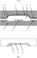
- the invention is based on the FIGS. 1 (a) to 1 (c) as well as the FIG. 2 be explained in more detail.
- FIG. 1a shows in cross-section a detail of a lid wafer 1 and a wafer associated therewith, containing active structures ("sensor wafer") 3.
- the cutout of the sensor wafer shows an active structure 4 to be protected, which is surrounded by an annular outer region, on the solder material. 5 is applied.
- the section of the lid wafer shows the corresponding area, wherein the annular outer area also has solder material 2 here. It should be understood that solder material does not necessarily have to be presented on both ring areas; As a rule, it is sufficient to provide this material only on one of the two wafers.
- the annular outer region of the lid wafer is adjoined inwardly by an annular region 10 and an inner region 11. In the illustrated embodiment, these two regions are configured as a cavity for receiving the active structure 4, wherein the region 10 at an angle ⁇ from the plane of the inside of the lid springs back (see Fig.
- ⁇ has a value of preferably 45 ° to 90 °, more preferably 48 ° to 65 °, and most preferably about 54 °.
- the lid wafer may be planar or otherwise domed while the active structure is housed in a recess of the bottom wafer.
- a buffer layer 6 is applied to the cover wafer or else to the sensor wafer between the active structure and the annular outer region applied.
- This buffer layer can be either structured, for example in the form of radially inwardly pointing webs, or over the entire surface (as a ring or the area completely filling surface) are applied in the cavities of the lid or sensor wafer.
- a multilayer system is in FIG. 2 shown schematically. It is especially to be envisaged when, for example, a bonding agent 15 and / or a gas barrier layer 14 are required under the buffer cover layer 13 or their presence leads to advantageous effects.
- the lid wafer is connected to the wafer containing the active structures via the respective annular outer regions (the connection region is in FIG. 1b denoted by 7), a metallic or metal-containing (eg eutectic AuSi) solder 8 is formed (see Figures 1b and 1c ).
- the buffer layer absorbs excess solder and ensures controlled wetting. Without a buffer layer, the solder would accumulate uncontrollably in lumps on surfaces which are poorly wettable by metals, such as, for example, oxidic surfaces or silicon, which can be deposited on the sensor structure and thus provoke a failure of the component.
- individual component covers can be connected to corresponding substrates having one or more active structures.
- the figures can be read for this embodiment as a representation of substrates 3 with component lids 1, which can be connected to be used in microsystems technology components.
- the advantage of the integration of the inventively provided buffer layer is thus in the increase of the manufacturing yield and in the prevention of failures of the component during operation, and thus leads to a more cost-effective production of microsystem technical hermetically encapsulated components.
- the provision of the buffer layer is advantageously carried out by vapor deposition of a metal layer or by sequential vapor deposition of a plurality of metal layers. It is favorable to provide an additionally applied metallic electroplating layer.
- the vapor deposition can be done on all sides or with the help of suitable masks, if structured layers are desired.
- the wetting angle of the buffer layer is advantageously less than 35 °; it is preferably less than 12 °, and more preferably less than 9 °.
- the buffer layer preferably has a metallic cover layer 13, wherein the metal of the cover layer may be selected from precious metals, in particular gold, copper and silver, nickel and nickel alloys such as a nickel / silver alloy, and oxide-free non-noble metals and semi-metals. Gold is particularly preferred among these. If an adhesion promoter layer 15 and / or a barrier layer 14 are present under the cover layer, it is preferred that the material of the layer under the cover layer be tungsten, titanium, chromium, an alloy of the aforementioned metals with a further metal, an alloy of two or three the aforementioned metals, nickel (under the condition that the cover layer is not formed exclusively of nickel), a nickel alloy, in particular a nickel-vanadium alloy, palladium or platinum.
- precious metals in particular gold, copper and silver, nickel and nickel alloys such as a nickel / silver alloy, and oxide-free non-noble metals and semi-metals. Gold is particularly preferred among these.
- a barrier layer may be below the cover layer and an adhesion promoter layer below it.
- the primer layer may have a thickness of about 5 to 100, preferably 20-100 nm
- the barrier layer may have a thickness of about 30-400 nm
- the top layer may have a thickness of about 100 nm to about 800 nm , preferably up to about 500 nm.
- the annular portion (s) 10 and / or inner region (s) 11 may be provided with a getter layer for absorbing unwanted gases, preferably the getter layer should be below the buffer layer or (directly) below the cover layer.
- some or all outer sides of the lid wafer are covered with a cover layer of gold. After connecting the lid wafer with the wafer containing the active structures, the individual components can be separated therefrom, which usually takes place in a sawing path.
Landscapes
- Engineering & Computer Science (AREA)
- Microelectronics & Electronic Packaging (AREA)
- Manufacturing & Machinery (AREA)
- Mechanical Engineering (AREA)
- Micromachines (AREA)
Applications Claiming Priority (2)
| Application Number | Priority Date | Filing Date | Title |
|---|---|---|---|
| DE102005053722A DE102005053722B4 (de) | 2005-11-10 | 2005-11-10 | Deckelwafer, in der Mikrosystemtechnik einsetzbares Bauelement mit einem solchen Wafer sowie Lötverfahren zum Verbinden entsprechender Bauelement-Teile |
| PCT/EP2006/068252 WO2007054524A1 (de) | 2005-11-10 | 2006-11-08 | Deckelwafer bzw. bauelement-deckel, waferbauteil bzw. in der mikrosystemtechnik einsetzbares bauelement sowie lötverfahren zum verbinden entsprechender wafer- bzw. bauelement-teile |
Publications (2)
| Publication Number | Publication Date |
|---|---|
| EP1945563A1 EP1945563A1 (de) | 2008-07-23 |
| EP1945563B1 true EP1945563B1 (de) | 2018-10-31 |
Family
ID=37877074
Family Applications (1)
| Application Number | Title | Priority Date | Filing Date |
|---|---|---|---|
| EP06819339.0A Active EP1945563B1 (de) | 2005-11-10 | 2006-11-08 | In der mikrosystemtechnik einsetzbares bauelement sowie lötverfahren zum verbinden entsprechender wafer- bzw. bauelement-teile |
Country Status (6)
| Country | Link |
|---|---|
| US (1) | US8039950B2 (enExample) |
| EP (1) | EP1945563B1 (enExample) |
| JP (1) | JP5243962B2 (enExample) |
| KR (1) | KR101416773B1 (enExample) |
| DE (1) | DE102005053722B4 (enExample) |
| WO (1) | WO2007054524A1 (enExample) |
Families Citing this family (16)
| Publication number | Priority date | Publication date | Assignee | Title |
|---|---|---|---|---|
| DE102005053722B4 (de) | 2005-11-10 | 2007-08-16 | Fraunhofer-Gesellschaft zur Förderung der angewandten Forschung e.V. | Deckelwafer, in der Mikrosystemtechnik einsetzbares Bauelement mit einem solchen Wafer sowie Lötverfahren zum Verbinden entsprechender Bauelement-Teile |
| JP4915677B2 (ja) * | 2008-05-27 | 2012-04-11 | パナソニック株式会社 | センサ装置の製造方法 |
| US7846815B2 (en) * | 2009-03-30 | 2010-12-07 | Freescale Semiconductor, Inc. | Eutectic flow containment in a semiconductor fabrication process |
| EP2264765A1 (en) | 2009-06-19 | 2010-12-22 | Fraunhofer-Gesellschaft zur Förderung der angewandten Forschung e.V. | Housing for an infrared radiation micro device and method for fabricating such housing |
| JP2012064673A (ja) * | 2010-09-14 | 2012-03-29 | Daishinku Corp | 電子部品パッケージ、及び電子部品パッケージの製造方法 |
| FR2967302B1 (fr) * | 2010-11-09 | 2012-12-21 | Commissariat Energie Atomique | Structure d'encapsulation d'un micro-dispositif comportant un matériau getter |
| JP5614724B2 (ja) | 2011-01-31 | 2014-10-29 | 日立金属株式会社 | 光電変換モジュール及び光電変換モジュールの製造方法 |
| JP5610156B2 (ja) * | 2011-01-31 | 2014-10-22 | 日立金属株式会社 | 光電変換モジュール及び光電変換モジュールの製造方法 |
| JP2014128842A (ja) * | 2012-12-28 | 2014-07-10 | Yamaha Corp | Mems素子を有する半導体パッケージ |
| US9764946B2 (en) * | 2013-10-24 | 2017-09-19 | Analog Devices, Inc. | MEMs device with outgassing shield |
| FR3014240B1 (fr) | 2013-11-29 | 2017-05-05 | Commissariat Energie Atomique | Procede de realisation d'un substrat comportant un materiau getter dispose sur des parois d'un ou plusieurs trous borgnes formes dans le substrat |
| KR20170119155A (ko) * | 2016-04-18 | 2017-10-26 | 주식회사 스탠딩에그 | 벌크 실리콘 멤스의 제조 방법 |
| KR20200032361A (ko) * | 2018-09-18 | 2020-03-26 | 삼성전기주식회사 | Mems 디바이스 |
| FI131434B1 (en) * | 2020-01-24 | 2025-04-22 | Teknologian Tutkimuskeskus Vtt Oy | Wafer level package for device |
| CN114211148B (zh) * | 2021-12-17 | 2023-07-25 | 西北电子装备技术研究所(中国电子科技集团公司第二研究所) | 高真空状态下微电子封装自动对位平行封焊机构 |
| KR102731140B1 (ko) * | 2022-04-01 | 2024-11-18 | 한국기술교육대학교 산학협력단 | 미세 구조물 제조 방법 |
Family Cites Families (15)
| Publication number | Priority date | Publication date | Assignee | Title |
|---|---|---|---|---|
| DE19537814B4 (de) * | 1995-10-11 | 2009-11-19 | Robert Bosch Gmbh | Sensor und Verfahren zur Herstellung eines Sensors |
| DE19711283A1 (de) * | 1997-03-18 | 1998-10-29 | Siemens Ag | Hermetisch dichtes optisches Sendemodul |
| JP3702612B2 (ja) | 1997-10-07 | 2005-10-05 | 株式会社デンソー | 半導体装置の製造方法 |
| US6778041B2 (en) * | 1998-06-02 | 2004-08-17 | Matsushita Electric Industrial Co., Ltd. | Millimeter wave module and radio apparatus |
| US6062461A (en) * | 1998-06-03 | 2000-05-16 | Delphi Technologies, Inc. | Process for bonding micromachined wafers using solder |
| ATE340761T1 (de) | 1999-12-15 | 2006-10-15 | Asulab Sa | Hermetische in-situ-gehäusungsmethode von mikrosystemen |
| DE10005555A1 (de) * | 2000-02-09 | 2001-08-16 | Bosch Gmbh Robert | Mikromechanisches Bauelement und entsprechendes Herstellungsverfahren |
| TW560018B (en) * | 2001-10-30 | 2003-11-01 | Asia Pacific Microsystems Inc | A wafer level packaged structure and method for manufacturing the same |
| ATE354538T1 (de) | 2002-04-11 | 2007-03-15 | Koninkl Philips Electronics Nv | Hertsellungsverfahren einer elektronischen vorrichtung in einem hohlraum mit einer bedeckung |
| JP2004202604A (ja) * | 2002-12-24 | 2004-07-22 | Aisin Seiki Co Ltd | パッケージ構造および製造方法 |
| US6953990B2 (en) * | 2003-09-19 | 2005-10-11 | Agilent Technologies, Inc. | Wafer-level packaging of optoelectronic devices |
| US7129576B2 (en) * | 2003-09-26 | 2006-10-31 | Tessera, Inc. | Structure and method of making capped chips including vertical interconnects having stud bumps engaged to surfaces of said caps |
| EP1683209A2 (en) | 2003-11-12 | 2006-07-26 | E.I. Dupont De Nemours And Company | Encapsulation assembly for electronic devices |
| US7211881B2 (en) * | 2004-03-24 | 2007-05-01 | Hewlett-Packard Development Company, L.P. | Structure for containing desiccant |
| DE102005053722B4 (de) | 2005-11-10 | 2007-08-16 | Fraunhofer-Gesellschaft zur Förderung der angewandten Forschung e.V. | Deckelwafer, in der Mikrosystemtechnik einsetzbares Bauelement mit einem solchen Wafer sowie Lötverfahren zum Verbinden entsprechender Bauelement-Teile |
-
2005
- 2005-11-10 DE DE102005053722A patent/DE102005053722B4/de not_active Expired - Lifetime
-
2006
- 2006-11-08 US US12/092,892 patent/US8039950B2/en active Active
- 2006-11-08 JP JP2008539432A patent/JP5243962B2/ja active Active
- 2006-11-08 WO PCT/EP2006/068252 patent/WO2007054524A1/de not_active Ceased
- 2006-11-08 EP EP06819339.0A patent/EP1945563B1/de active Active
- 2006-11-08 KR KR1020087012255A patent/KR101416773B1/ko active Active
Non-Patent Citations (1)
| Title |
|---|
| None * |
Also Published As
| Publication number | Publication date |
|---|---|
| US8039950B2 (en) | 2011-10-18 |
| JP2009516365A (ja) | 2009-04-16 |
| JP5243962B2 (ja) | 2013-07-24 |
| KR101416773B1 (ko) | 2014-08-06 |
| DE102005053722A1 (de) | 2007-05-24 |
| KR20080075122A (ko) | 2008-08-14 |
| EP1945563A1 (de) | 2008-07-23 |
| US20080317995A1 (en) | 2008-12-25 |
| WO2007054524A1 (de) | 2007-05-18 |
| DE102005053722B4 (de) | 2007-08-16 |
Similar Documents
| Publication | Publication Date | Title |
|---|---|---|
| EP1945563B1 (de) | In der mikrosystemtechnik einsetzbares bauelement sowie lötverfahren zum verbinden entsprechender wafer- bzw. bauelement-teile | |
| DE102009029180B4 (de) | Mikrosystem | |
| DE102011016554B4 (de) | Waferlevel-Package und Verfahren zur Herstellung | |
| DE102009029577B3 (de) | Verfahren zur Herstellung eines hochtemperaturfesten Leistungshalbleitermoduls | |
| DE102006019080B3 (de) | Herstellungsverfahren für ein gehäustes Bauelement | |
| DE10164502B4 (de) | Verfahren zur hermetischen Verkapselung eines Bauelements | |
| EP3055095B1 (de) | Verfahren zur herstellung einer metall-keramiklötverbindung | |
| DE4135189B4 (de) | Verfahren zur Montage des Gehäuses eines Halbleiter-Bauelements | |
| WO2004019490A1 (de) | Verkapseltes elektronisches bauelement und verfhren zur herstellung | |
| DE112010000715B4 (de) | Bauteilanordnung und Verfahren zu dessen Herstellung | |
| DE102007025992A1 (de) | Verfahren zur Herstellung eines MEMS-Packages | |
| DE102014202808A1 (de) | Verfahren zum eutektischen Bonden zweier Trägereinrichtungen | |
| EP2303769A2 (de) | Verkapselung, mems sowie verfahren zum selektiven verkapseln | |
| DE2314731B2 (de) | Halbleiteranordnung mit höckerartigen Vorsprüngen auf Kontaktflecken und Verfahren zur Herstellung einer solchen Halbleiteranordnung | |
| CH698772B1 (de) | Hermetisch abdichtende Kappe, Aufnahmegehäuse für eine elektronische Komponente und Verfahren zur Herstellung eines Aufnahmegehäuses für eine elektronische Komponente. | |
| DE102008028942A1 (de) | Halbleiterbauelement | |
| DE102016112200A1 (de) | Druckaufnehmer | |
| EP1727210B1 (de) | Verfahren zur Herstellung eines gehäuseabdichtenden Fensterelementes | |
| DE102004051442A1 (de) | Wafer-Level-Package-Herstellungsverfahren unter Verwendung von Laserbestrahlung | |
| WO2014019598A1 (de) | Substratverbund, verfahren und vorrichtung zum bonden von substraten | |
| DE102015101878A1 (de) | Mit Aktivlot versiegelte Mikrosystemtechnik-Bauelemente, Komponenten hierfür und Lottransferverfahren zu ihrer Herstellung | |
| DE102012219622B4 (de) | Mikrotechnologisches Bauelement mit Bondverbindung | |
| DE10126955A1 (de) | Integrierte Schaltung mit energieabsorbierender Struktur | |
| EP0186585B1 (en) | Die bonding process | |
| DE10140826B4 (de) | Verfahren zur mehrschrittigen Bearbeitung eines dünnen und unter den Bearbeitungsschritten bruchgefährdeten Halbleiter-Waferprodukts |
Legal Events
| Date | Code | Title | Description |
|---|---|---|---|
| PUAI | Public reference made under article 153(3) epc to a published international application that has entered the european phase |
Free format text: ORIGINAL CODE: 0009012 |
|
| 17P | Request for examination filed |
Effective date: 20080320 |
|
| AK | Designated contracting states |
Kind code of ref document: A1 Designated state(s): AT BE BG CH CY CZ DE DK EE ES FI FR GB GR HU IE IS IT LI LT LU LV MC NL PL PT RO SE SI SK TR |
|
| 17Q | First examination report despatched |
Effective date: 20090406 |
|
| DAX | Request for extension of the european patent (deleted) | ||
| RIC1 | Information provided on ipc code assigned before grant |
Ipc: B81C 1/00 20060101AFI20151210BHEP |
|
| STAA | Information on the status of an ep patent application or granted ep patent |
Free format text: STATUS: EXAMINATION IS IN PROGRESS |
|
| GRAP | Despatch of communication of intention to grant a patent |
Free format text: ORIGINAL CODE: EPIDOSNIGR1 |
|
| STAA | Information on the status of an ep patent application or granted ep patent |
Free format text: STATUS: GRANT OF PATENT IS INTENDED |
|
| INTG | Intention to grant announced |
Effective date: 20180611 |
|
| GRAS | Grant fee paid |
Free format text: ORIGINAL CODE: EPIDOSNIGR3 |
|
| GRAA | (expected) grant |
Free format text: ORIGINAL CODE: 0009210 |
|
| STAA | Information on the status of an ep patent application or granted ep patent |
Free format text: STATUS: THE PATENT HAS BEEN GRANTED |
|
| AK | Designated contracting states |
Kind code of ref document: B1 Designated state(s): AT BE BG CH CY CZ DE DK EE ES FI FR GB GR HU IE IS IT LI LT LU LV MC NL PL PT RO SE SI SK TR |
|
| REG | Reference to a national code |
Ref country code: CH Ref legal event code: EP Ref country code: GB Ref legal event code: FG4D Free format text: NOT ENGLISH |
|
| REG | Reference to a national code |
Ref country code: AT Ref legal event code: REF Ref document number: 1059143 Country of ref document: AT Kind code of ref document: T Effective date: 20181115 |
|
| REG | Reference to a national code |
Ref country code: DE Ref legal event code: R096 Ref document number: 502006016085 Country of ref document: DE |
|
| REG | Reference to a national code |
Ref country code: IE Ref legal event code: FG4D Free format text: LANGUAGE OF EP DOCUMENT: GERMAN |
|
| REG | Reference to a national code |
Ref country code: NL Ref legal event code: MP Effective date: 20181031 |
|
| REG | Reference to a national code |
Ref country code: LT Ref legal event code: MG4D |
|
| PG25 | Lapsed in a contracting state [announced via postgrant information from national office to epo] |
Ref country code: FI Free format text: LAPSE BECAUSE OF FAILURE TO SUBMIT A TRANSLATION OF THE DESCRIPTION OR TO PAY THE FEE WITHIN THE PRESCRIBED TIME-LIMIT Effective date: 20181031 Ref country code: BG Free format text: LAPSE BECAUSE OF FAILURE TO SUBMIT A TRANSLATION OF THE DESCRIPTION OR TO PAY THE FEE WITHIN THE PRESCRIBED TIME-LIMIT Effective date: 20190131 Ref country code: IS Free format text: LAPSE BECAUSE OF FAILURE TO SUBMIT A TRANSLATION OF THE DESCRIPTION OR TO PAY THE FEE WITHIN THE PRESCRIBED TIME-LIMIT Effective date: 20190228 Ref country code: ES Free format text: LAPSE BECAUSE OF FAILURE TO SUBMIT A TRANSLATION OF THE DESCRIPTION OR TO PAY THE FEE WITHIN THE PRESCRIBED TIME-LIMIT Effective date: 20181031 Ref country code: LV Free format text: LAPSE BECAUSE OF FAILURE TO SUBMIT A TRANSLATION OF THE DESCRIPTION OR TO PAY THE FEE WITHIN THE PRESCRIBED TIME-LIMIT Effective date: 20181031 Ref country code: PL Free format text: LAPSE BECAUSE OF FAILURE TO SUBMIT A TRANSLATION OF THE DESCRIPTION OR TO PAY THE FEE WITHIN THE PRESCRIBED TIME-LIMIT Effective date: 20181031 Ref country code: LT Free format text: LAPSE BECAUSE OF FAILURE TO SUBMIT A TRANSLATION OF THE DESCRIPTION OR TO PAY THE FEE WITHIN THE PRESCRIBED TIME-LIMIT Effective date: 20181031 |
|
| PG25 | Lapsed in a contracting state [announced via postgrant information from national office to epo] |
Ref country code: NL Free format text: LAPSE BECAUSE OF FAILURE TO SUBMIT A TRANSLATION OF THE DESCRIPTION OR TO PAY THE FEE WITHIN THE PRESCRIBED TIME-LIMIT Effective date: 20181031 Ref country code: PT Free format text: LAPSE BECAUSE OF FAILURE TO SUBMIT A TRANSLATION OF THE DESCRIPTION OR TO PAY THE FEE WITHIN THE PRESCRIBED TIME-LIMIT Effective date: 20190301 Ref country code: SE Free format text: LAPSE BECAUSE OF FAILURE TO SUBMIT A TRANSLATION OF THE DESCRIPTION OR TO PAY THE FEE WITHIN THE PRESCRIBED TIME-LIMIT Effective date: 20181031 Ref country code: GR Free format text: LAPSE BECAUSE OF FAILURE TO SUBMIT A TRANSLATION OF THE DESCRIPTION OR TO PAY THE FEE WITHIN THE PRESCRIBED TIME-LIMIT Effective date: 20190201 |
|
| REG | Reference to a national code |
Ref country code: CH Ref legal event code: PL |
|
| PG25 | Lapsed in a contracting state [announced via postgrant information from national office to epo] |
Ref country code: IT Free format text: LAPSE BECAUSE OF FAILURE TO SUBMIT A TRANSLATION OF THE DESCRIPTION OR TO PAY THE FEE WITHIN THE PRESCRIBED TIME-LIMIT Effective date: 20181031 Ref country code: CZ Free format text: LAPSE BECAUSE OF FAILURE TO SUBMIT A TRANSLATION OF THE DESCRIPTION OR TO PAY THE FEE WITHIN THE PRESCRIBED TIME-LIMIT Effective date: 20181031 Ref country code: DK Free format text: LAPSE BECAUSE OF FAILURE TO SUBMIT A TRANSLATION OF THE DESCRIPTION OR TO PAY THE FEE WITHIN THE PRESCRIBED TIME-LIMIT Effective date: 20181031 Ref country code: LU Free format text: LAPSE BECAUSE OF NON-PAYMENT OF DUE FEES Effective date: 20181108 |
|
| REG | Reference to a national code |
Ref country code: DE Ref legal event code: R097 Ref document number: 502006016085 Country of ref document: DE |
|
| REG | Reference to a national code |
Ref country code: BE Ref legal event code: MM Effective date: 20181130 |
|
| REG | Reference to a national code |
Ref country code: IE Ref legal event code: MM4A |
|
| PG25 | Lapsed in a contracting state [announced via postgrant information from national office to epo] |
Ref country code: MC Free format text: LAPSE BECAUSE OF FAILURE TO SUBMIT A TRANSLATION OF THE DESCRIPTION OR TO PAY THE FEE WITHIN THE PRESCRIBED TIME-LIMIT Effective date: 20181031 Ref country code: LI Free format text: LAPSE BECAUSE OF NON-PAYMENT OF DUE FEES Effective date: 20181130 Ref country code: EE Free format text: LAPSE BECAUSE OF FAILURE TO SUBMIT A TRANSLATION OF THE DESCRIPTION OR TO PAY THE FEE WITHIN THE PRESCRIBED TIME-LIMIT Effective date: 20181031 Ref country code: RO Free format text: LAPSE BECAUSE OF FAILURE TO SUBMIT A TRANSLATION OF THE DESCRIPTION OR TO PAY THE FEE WITHIN THE PRESCRIBED TIME-LIMIT Effective date: 20181031 Ref country code: SK Free format text: LAPSE BECAUSE OF FAILURE TO SUBMIT A TRANSLATION OF THE DESCRIPTION OR TO PAY THE FEE WITHIN THE PRESCRIBED TIME-LIMIT Effective date: 20181031 Ref country code: CH Free format text: LAPSE BECAUSE OF NON-PAYMENT OF DUE FEES Effective date: 20181130 |
|
| PLBE | No opposition filed within time limit |
Free format text: ORIGINAL CODE: 0009261 |
|
| STAA | Information on the status of an ep patent application or granted ep patent |
Free format text: STATUS: NO OPPOSITION FILED WITHIN TIME LIMIT |
|
| 26N | No opposition filed |
Effective date: 20190801 |
|
| PG25 | Lapsed in a contracting state [announced via postgrant information from national office to epo] |
Ref country code: IE Free format text: LAPSE BECAUSE OF NON-PAYMENT OF DUE FEES Effective date: 20181108 Ref country code: SI Free format text: LAPSE BECAUSE OF FAILURE TO SUBMIT A TRANSLATION OF THE DESCRIPTION OR TO PAY THE FEE WITHIN THE PRESCRIBED TIME-LIMIT Effective date: 20181031 |
|
| PG25 | Lapsed in a contracting state [announced via postgrant information from national office to epo] |
Ref country code: BE Free format text: LAPSE BECAUSE OF NON-PAYMENT OF DUE FEES Effective date: 20181130 |
|
| REG | Reference to a national code |
Ref country code: AT Ref legal event code: MM01 Ref document number: 1059143 Country of ref document: AT Kind code of ref document: T Effective date: 20181108 |
|
| PG25 | Lapsed in a contracting state [announced via postgrant information from national office to epo] |
Ref country code: AT Free format text: LAPSE BECAUSE OF NON-PAYMENT OF DUE FEES Effective date: 20181108 |
|
| PG25 | Lapsed in a contracting state [announced via postgrant information from national office to epo] |
Ref country code: TR Free format text: LAPSE BECAUSE OF FAILURE TO SUBMIT A TRANSLATION OF THE DESCRIPTION OR TO PAY THE FEE WITHIN THE PRESCRIBED TIME-LIMIT Effective date: 20181031 |
|
| PG25 | Lapsed in a contracting state [announced via postgrant information from national office to epo] |
Ref country code: CY Free format text: LAPSE BECAUSE OF FAILURE TO SUBMIT A TRANSLATION OF THE DESCRIPTION OR TO PAY THE FEE WITHIN THE PRESCRIBED TIME-LIMIT Effective date: 20181031 Ref country code: HU Free format text: LAPSE BECAUSE OF FAILURE TO SUBMIT A TRANSLATION OF THE DESCRIPTION OR TO PAY THE FEE WITHIN THE PRESCRIBED TIME-LIMIT; INVALID AB INITIO Effective date: 20061108 |
|
| P01 | Opt-out of the competence of the unified patent court (upc) registered |
Effective date: 20230524 |
|
| PGFP | Annual fee paid to national office [announced via postgrant information from national office to epo] |
Ref country code: DE Payment date: 20241125 Year of fee payment: 19 |
|
| PGFP | Annual fee paid to national office [announced via postgrant information from national office to epo] |
Ref country code: GB Payment date: 20241126 Year of fee payment: 19 |
|
| PGFP | Annual fee paid to national office [announced via postgrant information from national office to epo] |
Ref country code: FR Payment date: 20241126 Year of fee payment: 19 |