EP1944165A2 - Betätigungsvorrichtung und Flüssigkeitsausgabekopf mit solcher Betätigungsvorrichtung - Google Patents
Betätigungsvorrichtung und Flüssigkeitsausgabekopf mit solcher Betätigungsvorrichtung Download PDFInfo
- Publication number
- EP1944165A2 EP1944165A2 EP08000484A EP08000484A EP1944165A2 EP 1944165 A2 EP1944165 A2 EP 1944165A2 EP 08000484 A EP08000484 A EP 08000484A EP 08000484 A EP08000484 A EP 08000484A EP 1944165 A2 EP1944165 A2 EP 1944165A2
- Authority
- EP
- European Patent Office
- Prior art keywords
- piezoelectric layer
- piezoelectric
- columnar crystals
- substrate
- lower electrode
- Prior art date
- Legal status (The legal status is an assumption and is not a legal conclusion. Google has not performed a legal analysis and makes no representation as to the accuracy of the status listed.)
- Withdrawn
Links
- 239000007788 liquid Substances 0.000 title claims description 23
- 239000000758 substrate Substances 0.000 claims abstract description 61
- 239000013078 crystal Substances 0.000 claims abstract description 56
- 239000012212 insulator Substances 0.000 description 15
- 230000001681 protective effect Effects 0.000 description 11
- 229910052451 lead zirconate titanate Inorganic materials 0.000 description 8
- 239000000463 material Substances 0.000 description 8
- HFGPZNIAWCZYJU-UHFFFAOYSA-N lead zirconate titanate Chemical compound [O-2].[O-2].[O-2].[O-2].[O-2].[Ti+4].[Zr+4].[Pb+2] HFGPZNIAWCZYJU-UHFFFAOYSA-N 0.000 description 5
- VYPSYNLAJGMNEJ-UHFFFAOYSA-N Silicium dioxide Chemical compound O=[Si]=O VYPSYNLAJGMNEJ-UHFFFAOYSA-N 0.000 description 4
- 229910052746 lanthanum Inorganic materials 0.000 description 4
- 238000007789 sealing Methods 0.000 description 4
- XUIMIQQOPSSXEZ-UHFFFAOYSA-N Silicon Chemical compound [Si] XUIMIQQOPSSXEZ-UHFFFAOYSA-N 0.000 description 3
- 239000010931 gold Substances 0.000 description 3
- 229910052710 silicon Inorganic materials 0.000 description 3
- 239000010703 silicon Substances 0.000 description 3
- 239000004734 Polyphenylene sulfide Substances 0.000 description 2
- RTAQQCXQSZGOHL-UHFFFAOYSA-N Titanium Chemical compound [Ti] RTAQQCXQSZGOHL-UHFFFAOYSA-N 0.000 description 2
- 239000000853 adhesive Substances 0.000 description 2
- 230000001070 adhesive effect Effects 0.000 description 2
- PCHJSUWPFVWCPO-UHFFFAOYSA-N gold Chemical compound [Au] PCHJSUWPFVWCPO-UHFFFAOYSA-N 0.000 description 2
- 229910052737 gold Inorganic materials 0.000 description 2
- FZLIPJUXYLNCLC-UHFFFAOYSA-N lanthanum atom Chemical compound [La] FZLIPJUXYLNCLC-UHFFFAOYSA-N 0.000 description 2
- 239000011777 magnesium Substances 0.000 description 2
- 238000004519 manufacturing process Methods 0.000 description 2
- RVTZCBVAJQQJTK-UHFFFAOYSA-N oxygen(2-);zirconium(4+) Chemical compound [O-2].[O-2].[Zr+4] RVTZCBVAJQQJTK-UHFFFAOYSA-N 0.000 description 2
- 238000005192 partition Methods 0.000 description 2
- BASFCYQUMIYNBI-UHFFFAOYSA-N platinum Chemical compound [Pt] BASFCYQUMIYNBI-UHFFFAOYSA-N 0.000 description 2
- 229920000069 polyphenylene sulfide Polymers 0.000 description 2
- 239000000377 silicon dioxide Substances 0.000 description 2
- 235000012239 silicon dioxide Nutrition 0.000 description 2
- 238000004544 sputter deposition Methods 0.000 description 2
- 229910001220 stainless steel Inorganic materials 0.000 description 2
- 239000010935 stainless steel Substances 0.000 description 2
- 229910001928 zirconium oxide Inorganic materials 0.000 description 2
- 238000000018 DNA microarray Methods 0.000 description 1
- FYYHWMGAXLPEAU-UHFFFAOYSA-N Magnesium Chemical compound [Mg] FYYHWMGAXLPEAU-UHFFFAOYSA-N 0.000 description 1
- 229910020294 Pb(Zr,Ti)O3 Inorganic materials 0.000 description 1
- 229910003781 PbTiO3 Inorganic materials 0.000 description 1
- 229910020698 PbZrO3 Inorganic materials 0.000 description 1
- 229910010252 TiO3 Inorganic materials 0.000 description 1
- 239000000919 ceramic Substances 0.000 description 1
- 239000003086 colorant Substances 0.000 description 1
- 238000000354 decomposition reaction Methods 0.000 description 1
- 239000003989 dielectric material Substances 0.000 description 1
- NKZSPGSOXYXWQA-UHFFFAOYSA-N dioxido(oxo)titanium;lead(2+) Chemical compound [Pb+2].[O-][Ti]([O-])=O NKZSPGSOXYXWQA-UHFFFAOYSA-N 0.000 description 1
- 238000001035 drying Methods 0.000 description 1
- 239000007772 electrode material Substances 0.000 description 1
- 238000005530 etching Methods 0.000 description 1
- 229910002112 ferroelectric ceramic material Inorganic materials 0.000 description 1
- 238000010304 firing Methods 0.000 description 1
- 239000011521 glass Substances 0.000 description 1
- 239000002241 glass-ceramic Substances 0.000 description 1
- 229910052741 iridium Inorganic materials 0.000 description 1
- GKOZUEZYRPOHIO-UHFFFAOYSA-N iridium atom Chemical compound [Ir] GKOZUEZYRPOHIO-UHFFFAOYSA-N 0.000 description 1
- 239000004973 liquid crystal related substance Substances 0.000 description 1
- 229910052749 magnesium Inorganic materials 0.000 description 1
- 239000000395 magnesium oxide Substances 0.000 description 1
- CPLXHLVBOLITMK-UHFFFAOYSA-N magnesium oxide Inorganic materials [Mg]=O CPLXHLVBOLITMK-UHFFFAOYSA-N 0.000 description 1
- AXZKOIWUVFPNLO-UHFFFAOYSA-N magnesium;oxygen(2-) Chemical compound [O-2].[Mg+2] AXZKOIWUVFPNLO-UHFFFAOYSA-N 0.000 description 1
- 229910052751 metal Inorganic materials 0.000 description 1
- 239000002184 metal Substances 0.000 description 1
- 229910044991 metal oxide Inorganic materials 0.000 description 1
- 150000004706 metal oxides Chemical class 0.000 description 1
- 238000000034 method Methods 0.000 description 1
- 239000000203 mixture Substances 0.000 description 1
- 229910000480 nickel oxide Inorganic materials 0.000 description 1
- 229910052758 niobium Inorganic materials 0.000 description 1
- 239000010955 niobium Substances 0.000 description 1
- 229910000484 niobium oxide Inorganic materials 0.000 description 1
- URLJKFSTXLNXLG-UHFFFAOYSA-N niobium(5+);oxygen(2-) Chemical compound [O-2].[O-2].[O-2].[O-2].[O-2].[Nb+5].[Nb+5] URLJKFSTXLNXLG-UHFFFAOYSA-N 0.000 description 1
- 230000003647 oxidation Effects 0.000 description 1
- 238000007254 oxidation reaction Methods 0.000 description 1
- GNRSAWUEBMWBQH-UHFFFAOYSA-N oxonickel Chemical compound [Ni]=O GNRSAWUEBMWBQH-UHFFFAOYSA-N 0.000 description 1
- 238000000059 patterning Methods 0.000 description 1
- 229910052697 platinum Inorganic materials 0.000 description 1
- 239000004065 semiconductor Substances 0.000 description 1
- 238000003980 solgel method Methods 0.000 description 1
- 239000002904 solvent Substances 0.000 description 1
- 239000000126 substance Substances 0.000 description 1
- 238000003466 welding Methods 0.000 description 1
Images
Classifications
-
- B—PERFORMING OPERATIONS; TRANSPORTING
- B41—PRINTING; LINING MACHINES; TYPEWRITERS; STAMPS
- B41J—TYPEWRITERS; SELECTIVE PRINTING MECHANISMS, i.e. MECHANISMS PRINTING OTHERWISE THAN FROM A FORME; CORRECTION OF TYPOGRAPHICAL ERRORS
- B41J2/00—Typewriters or selective printing mechanisms characterised by the printing or marking process for which they are designed
- B41J2/005—Typewriters or selective printing mechanisms characterised by the printing or marking process for which they are designed characterised by bringing liquid or particles selectively into contact with a printing material
- B41J2/01—Ink jet
- B41J2/135—Nozzles
- B41J2/14—Structure thereof only for on-demand ink jet heads
- B41J2/14201—Structure of print heads with piezoelectric elements
- B41J2/14233—Structure of print heads with piezoelectric elements of film type, deformed by bending and disposed on a diaphragm
-
- H—ELECTRICITY
- H10—SEMICONDUCTOR DEVICES; ELECTRIC SOLID-STATE DEVICES NOT OTHERWISE PROVIDED FOR
- H10N—ELECTRIC SOLID-STATE DEVICES NOT OTHERWISE PROVIDED FOR
- H10N30/00—Piezoelectric or electrostrictive devices
- H10N30/20—Piezoelectric or electrostrictive devices with electrical input and mechanical output, e.g. functioning as actuators or vibrators
- H10N30/204—Piezoelectric or electrostrictive devices with electrical input and mechanical output, e.g. functioning as actuators or vibrators using bending displacement, e.g. unimorph, bimorph or multimorph cantilever or membrane benders
- H10N30/2047—Membrane type
-
- H—ELECTRICITY
- H10—SEMICONDUCTOR DEVICES; ELECTRIC SOLID-STATE DEVICES NOT OTHERWISE PROVIDED FOR
- H10N—ELECTRIC SOLID-STATE DEVICES NOT OTHERWISE PROVIDED FOR
- H10N30/00—Piezoelectric or electrostrictive devices
- H10N30/704—Piezoelectric or electrostrictive devices based on piezoelectric or electrostrictive films or coatings
-
- H—ELECTRICITY
- H10—SEMICONDUCTOR DEVICES; ELECTRIC SOLID-STATE DEVICES NOT OTHERWISE PROVIDED FOR
- H10N—ELECTRIC SOLID-STATE DEVICES NOT OTHERWISE PROVIDED FOR
- H10N30/00—Piezoelectric or electrostrictive devices
- H10N30/80—Constructional details
- H10N30/87—Electrodes or interconnections, e.g. leads or terminals
-
- B—PERFORMING OPERATIONS; TRANSPORTING
- B41—PRINTING; LINING MACHINES; TYPEWRITERS; STAMPS
- B41J—TYPEWRITERS; SELECTIVE PRINTING MECHANISMS, i.e. MECHANISMS PRINTING OTHERWISE THAN FROM A FORME; CORRECTION OF TYPOGRAPHICAL ERRORS
- B41J2/00—Typewriters or selective printing mechanisms characterised by the printing or marking process for which they are designed
- B41J2/005—Typewriters or selective printing mechanisms characterised by the printing or marking process for which they are designed characterised by bringing liquid or particles selectively into contact with a printing material
- B41J2/01—Ink jet
- B41J2/135—Nozzles
- B41J2/14—Structure thereof only for on-demand ink jet heads
- B41J2/14201—Structure of print heads with piezoelectric elements
- B41J2/14233—Structure of print heads with piezoelectric elements of film type, deformed by bending and disposed on a diaphragm
- B41J2002/14241—Structure of print heads with piezoelectric elements of film type, deformed by bending and disposed on a diaphragm having a cover around the piezoelectric thin film element
-
- B—PERFORMING OPERATIONS; TRANSPORTING
- B41—PRINTING; LINING MACHINES; TYPEWRITERS; STAMPS
- B41J—TYPEWRITERS; SELECTIVE PRINTING MECHANISMS, i.e. MECHANISMS PRINTING OTHERWISE THAN FROM A FORME; CORRECTION OF TYPOGRAPHICAL ERRORS
- B41J2/00—Typewriters or selective printing mechanisms characterised by the printing or marking process for which they are designed
- B41J2/005—Typewriters or selective printing mechanisms characterised by the printing or marking process for which they are designed characterised by bringing liquid or particles selectively into contact with a printing material
- B41J2/01—Ink jet
- B41J2/135—Nozzles
- B41J2/14—Structure thereof only for on-demand ink jet heads
- B41J2002/14419—Manifold
-
- B—PERFORMING OPERATIONS; TRANSPORTING
- B41—PRINTING; LINING MACHINES; TYPEWRITERS; STAMPS
- B41J—TYPEWRITERS; SELECTIVE PRINTING MECHANISMS, i.e. MECHANISMS PRINTING OTHERWISE THAN FROM A FORME; CORRECTION OF TYPOGRAPHICAL ERRORS
- B41J2/00—Typewriters or selective printing mechanisms characterised by the printing or marking process for which they are designed
- B41J2/005—Typewriters or selective printing mechanisms characterised by the printing or marking process for which they are designed characterised by bringing liquid or particles selectively into contact with a printing material
- B41J2/01—Ink jet
- B41J2/135—Nozzles
- B41J2/14—Structure thereof only for on-demand ink jet heads
- B41J2002/14491—Electrical connection
-
- B—PERFORMING OPERATIONS; TRANSPORTING
- B41—PRINTING; LINING MACHINES; TYPEWRITERS; STAMPS
- B41J—TYPEWRITERS; SELECTIVE PRINTING MECHANISMS, i.e. MECHANISMS PRINTING OTHERWISE THAN FROM A FORME; CORRECTION OF TYPOGRAPHICAL ERRORS
- B41J2202/00—Embodiments of or processes related to ink-jet or thermal heads
- B41J2202/01—Embodiments of or processes related to ink-jet heads
- B41J2202/11—Embodiments of or processes related to ink-jet heads characterised by specific geometrical characteristics
-
- H—ELECTRICITY
- H10—SEMICONDUCTOR DEVICES; ELECTRIC SOLID-STATE DEVICES NOT OTHERWISE PROVIDED FOR
- H10N—ELECTRIC SOLID-STATE DEVICES NOT OTHERWISE PROVIDED FOR
- H10N30/00—Piezoelectric or electrostrictive devices
- H10N30/80—Constructional details
- H10N30/85—Piezoelectric or electrostrictive active materials
- H10N30/853—Ceramic compositions
- H10N30/8548—Lead-based oxides
- H10N30/8554—Lead-zirconium titanate [PZT] based
Definitions
- the present invention relates to actuator devices having vibrating plates and piezoelectric elements that are displaceably provided on a substrate, and also relates to liquid ejecting heads including the actuator devices.
- Examples of a piezoelectric element included in an actuator device include a structure in which a piezoelectric material functioning as an electromechanical transducer, such as a piezoelectric layer made of a crystallized dielectric material, is disposed between two electrodes, a lower electrode and an upper electrode.
- a piezoelectric material functioning as an electromechanical transducer such as a piezoelectric layer made of a crystallized dielectric material
- Such an actuator device is called, in general, a flexural-oscillation-mode actuator device, and is used as a component of a liquid ejecting head, for example.
- Typical examples of the liquid ejecting head include an ink jet recording head in which ink droplets are ejected through nozzle openings by utilizing deformation of vibrating plates, which constitute part of pressure-generating chambers communicating with the nozzle openings, caused by piezoelectric elements so as to pressurize the ink in the pressure-generating chambers.
- Examples of the actuator device included in the ink jet recording head include a device in which a piezoelectric element is formed independently for each of the pressure-generating chambers by lithographically dividing a piezoelectric material layer, which is uniformly deposited over the entire surface of the vibrating plates, in correspondence with the pressure-generating chambers.
- JP-A-2002-314163 , JP-A-2002-319714 , and JP-A-2003-174211 disclose examples of such a piezoelectric element including a lower electrode disposed on a substrate, a piezoelectric layer disposed on the lower electrode, and an upper electrode disposed on the piezoelectric layer such that an end face of the lower electrode and the top surface of the substrate become perpendicular to each other.
- An advantage of some aspects of the invention is that it provides an actuator device including a piezoelectric layer having a high strength against a stress occurring upon application of a voltage to a pair of electrodes, and also provides a liquid ejecting head including the actuator device.
- an actuator device includes a piezoelectric element including a lower electrode, a piezoelectric layer, and an upper electrode that are displaceably provided in sequence on a substrate.
- the lower electrode includes a flat portion at a central region thereof and an inclined portion at an end thereof descending toward the substrate.
- the piezoelectric layer is disposed above the lower electrode and the substrate, and includes a first piezoelectric layer portion constituted by a plurality of columnar crystals extending orthogonally to a surface of the flat portion of the lower electrode, a second piezoelectric layer portion constituted by a plurality of columnar crystals extending orthogonally to a surface of the substrate, and a third piezoelectric layer portion constituted by a plurality of columnar crystals residing on the inclined portion between the first and second piezoelectric layer portions.
- the columnar crystals of the third piezoelectric layer portion extend orthogonally to a surface of the inclined portion and bend toward the upper electrode so as to extend orthogonally to the surface of the substrate.
- Grains of the columnar crystals constituting the third piezoelectric layer portion have larger widths than those of grains of the columnar crystals constituting the first and second piezoelectric layer portions at a surface of the piezoelectric layer proximate to the upper electrode.
- the columnar crystals constituting the piezoelectric layer portion at the intermediate piezoelectric region have a high strength against a stress applied in a direction from the lower electrode toward the upper electrode or in the opposite direction.
- a highly reliable and durable actuator device can be provided.
- the piezoelectric element include an active piezoelectric region constituted by the first piezoelectric layer portion, an inactive piezoelectric region constituted by the second piezoelectric layer portion, and an intermediate piezoelectric region constituted by the third piezoelectric layer portion.
- the presence of the intermediate piezoelectric region constituted by highly strong columnar crystals relaxes a stress occurring at the boundary between the active piezoelectric region and the inactive piezoelectric region.
- a more highly reliable and durable actuator device can be provided.
- the grains of the columnar crystals constituting the third piezoelectric layer portion have larger widths than those of the grains of the columnar crystals constituting the first and second piezoelectric layer portions in the same direction. This provides the columnar crystals constituting the piezoelectric layer portion at the intermediate piezoelectric region with a higher strength against a stress applied in a direction from the lower electrode toward the upper electrode or in the opposite direction. Thus, a more highly reliable and durable actuator device can be provided.
- a width direction of the grains of the columnar crystals constituting the third piezoelectric layer portion correspond to an inclined direction of the inclined portion. This provides the columnar crystals constituting the piezoelectric layer portion at the intermediate piezoelectric region with a high strength against a stress applied in the inclined direction of the inclined portion from the lower electrode toward the upper electrode or in the opposite direction. Thus, a more highly reliable and durable actuator device can be provided.
- the inclined portion be inclined at 5 to 50 degrees with respect to the surface of the substrate. This provides the columnar crystals constituting the piezoelectric layer portion at the intermediate piezoelectric region with a higher strength against a stress applied in the inclined direction of the inclined portion from the lower electrode toward the upper electrode or in the opposite direction.
- the inclined portion have a length of 0.5 to 3 ⁇ m in the inclined direction. This provides the columnar crystals constituting the piezoelectric layer portion at the intermediate piezoelectric region with a higher strength against a stress applied in the inclined direction of the inclined portion from the lower electrode toward the upper electrode or in the opposite direction.
- the columnar crystals respectively constituting the first to third piezoelectric layer portions have perovskite structures. This provides the columnar crystals constituting the piezoelectric layer portion at the intermediate piezoelectric region with a higher strength against a stress applied in a direction from the lower electrode toward the upper electrode or in the opposite direction.
- a liquid ejecting head includes a channel-forming substrate provided with a pressure-generating chamber communicating with a nozzle opening through which liquid is ejected, and the actuator device according to the first aspect of the invention serving as a liquid ejecting unit that is provided on one surface of the channel-forming substrate and causes a change of pressure in the pressure-generating chamber.
- the liquid ejecting head according to the second aspect of the invention includes the actuator device having the intermediate piezoelectric region constituted by columnar crystals having a high strength.
- the actuator device having the intermediate piezoelectric region constituted by columnar crystals having a high strength.
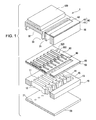
- Fig. 1 is a schematic exploded perspective view of a recording head according to a first embodiment.
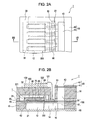
- Fig. 2A is a plan view of the recording head according to the first embodiment.
- Fig. 2B is a sectional view of the recording head according to the first embodiment.
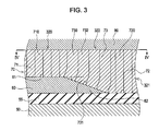
- Fig. 3 is an enlarged sectional view of a piezoelectric element according to the first embodiment.
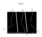
- Fig. 4 schematically shows a surface taken along plane IV-IV in Fig. 3 .
- Fig. 1 is a schematic exploded perspective view of an ink jet recording head I as an example of a liquid ejecting head according to a first embodiment of the invention.
- Figs. 2A and 2B are a plan view and a sectional view of the same, respectively, the sectional view being taken along line IIB-IIB in Fig. 1 .
- a channel-forming substrate 10 as a substrate is made of a silicon single crystal having a (110) crystal plane orientation.
- An elastic film 50 composed of silicon dioxide and having a thickness of 0.5 ⁇ m to 2 ⁇ m is preliminarily provided on a surface of the channel-forming substrate 10 by thermal oxidation.
- the channel-forming substrate 10 has pressure-generating chambers 12 arranged parallel with each other in the width direction (lateral direction) of the channel-forming substrate 10.
- the pressure-generating chambers 12 are defined by a plurality of partitions 11 that are formed by performing anisotropic etching on the other surface of the channel-forming substrate 10.
- Each of the partitions 11 further defines an ink supply channel 14 and a communicating channel 15 at an end in the longitudinal direction of a corresponding one of the pressure-generating chambers 12 of the channel-forming substrate 10.
- Each of the communicating channels 15 communicates at its one end with a communicating region 13 constituting a part of a reservoir 100 that serves as a common ink chamber (liquid chamber) for the pressure-generating chambers 12.
- the channel-forming substrate 10 has liquid channels each including the pressure-generating chamber 12, the communicating region 13, the ink supply channel 14, and the communicating channel 15.
- the ink supply channel 14 communicates with a longitudinal end of the corresponding pressure-generating chamber 12 and has a cross-section smaller than that of the pressure-generating chamber 12.
- a nozzle plate 20 has nozzle openings 21 bored therein, each of which communicates with the vicinity of an end of the corresponding pressure-generating chamber 12 opposite the end communicating with the ink supply channel 14.
- the nozzle plate 20 is bonded to an open surface of the channel-forming substrate 10 with an adhesive, a heat welding film, or the like.
- the nozzle plate 20 is made of, for example, a glass-ceramic plate, a silicon single-crystal substrate, or a stainless steel plate.
- the elastic film 50 composed of silicon dioxide and having a thickness of, for example, about 1.0 ⁇ m is provided on a surface of the channel-forming substrate 10 opposite the open surface.
- An insulator film 55 composed of zirconium oxide (ZrO 2 ) or the like, and having a thickness of, for example, about 0.4 ⁇ m is deposited on the elastic film 50.
- the insulator film 55 supports a plurality of stacks each including a lower electrode film 60 having a thickness of about 0.1 ⁇ m to 0.5 ⁇ m; a piezoelectric layer 70, which is a dielectric film and is to be described below in detail, composed of lead zirconate titanate (PZT) or the like and having a thickness of about 1.1 ⁇ m; and an upper electrode film 80 composed of gold, platinum, iridium, or the like and provided with a thickness of about 0.05 ⁇ m, for example, so as to cover the lower electrode film 60 together with the piezoelectric layer 70 disposed therebetween.
- PZT lead zirconate titanate
- an upper electrode film 80 composed of gold, platinum, iridium, or the like and provided with a thickness of about 0.05 ⁇ m, for example, so as to cover the lower electrode film 60 together with the piezoelectric layer 70 disposed therebetween.
- These stacks serve as piezoelectric elements 300.
- the lower electrode film 60 extends across all regions corresponding to the pressure-generating chambers 12, thereby serving as a common electrode for the piezoelectric elements 300.
- the lower electrode film 60 has inclined portions 62 at its ends in a direction in which the pressure-generating chambers 12 extend.
- the inclined portions 62 extend downward from the top surface of the lower electrode film 60 toward the channel-forming substrate 10.
- the piezoelectric layers 70 and the upper electrode films 80 extend beyond the inclined portions 62 so as to cover portions of the lower electrode film 60 in correspondence with the piezoelectric elements 300, whereby the upper electrode films 80 serve as individual electrodes for the piezoelectric elements 300.
- the elastic film 50, the insulator film 55, and the lower electrode film 60 constitute a vibrating plate.
- the vibrating plate and each piezoelectric element 300 constitute an actuator device 1.
- the piezoelectric element 300 refers to a structure including the lower electrode film 60, the piezoelectric layer 70, and the upper electrode film 80.
- the lower electrode film 60 serves as a common electrode for all the piezoelectric elements 300
- the upper electrode films 80 serve as individual electrodes for the piezoelectric elements 300.
- their roles may also be reversed in view of the arrangement of the driving circuit or wiring.
- an active piezoelectric region 320 is provided for each of the pressure-generating chambers 12.
- the piezoelectric layer 70 of the first embodiment is, for example, a crystal film provided on the lower electrode film 60 and having a perovskite structure made of a ferroelectric ceramic material functioning as an electromechanical transducer.
- the piezoelectric layer 70 is preferably composed of, for example, a ferroelectric-piezoelectric material such as lead zirconate titanate (PZT), or a mixture of the ferroelectric-piezoelectric material and a metaloxide such as niobium oxide, nickel oxide, or magnesium oxide.
- the piezoelectric layer 70 of the first embodiment is composed of lead zirconate titanate (PZT).
- the upper electrode film 80 that serves as the individual electrode of the piezoelectric element 300 is provided with a lead electrode 90 composed of gold (Au), for example, connected at an end of the upper electrode film 80 near the ink supply channel 14 and extending down onto the insulator film 55.
- a lead electrode 90 composed of gold (Au), for example, connected at an end of the upper electrode film 80 near the ink supply channel 14 and extending down onto the insulator film 55.
- the channel-forming substrate 10 having the piezoelectric elements 300 provided thereon has a protective substrate 30 bonded together with an adhesive 35 therebetween.
- the protective substrate 30 has a reservoir section 31 constituting at least a part of the reservoir 100.
- the reservoir section 31 of the first embodiment penetrates the protective substrate 30 thicknesswise and extends in the protective substrate 30 in the transverse direction of the pressure-generating chambers 12, thereby communicating with the communicating region 13.
- the reservoir section 31 and the communicating region 13 in the channel-forming substrate 10 communicate with each other and constitute the reservoir 100 that serves as the common liquid chamber of the pressure-generating chambers 12. It is also possible that the communicating region 13 in the channel-forming substrate 10 is divided into compartments corresponding to the pressure-generating chambers 12 to make only the reservoir section 31 serve as the reservoir.
- the pressure-generating chambers 12 are provided in the channel-forming substrate 10 and that the ink supply channels 14 communicating with the reservoir and the pressure-generating chambers 12 are provided in a member interposed between the channel-forming substrate 10 and the protective substrate 30 (for example, the elastic film 50 and the insulator film 55).
- the protective substrate 30 has a piezoelectric-element retaining section 32, which has an internal space large enough not to hinder operation of the piezoelectric elements 300, provided in a region over the piezoelectric elements 300.
- the piezoelectric-element retaining section 32 may be either sealed or unsealed, as long as it provides an internal space large enough not to hinder operation of the piezoelectric elements 300.
- the protective substrate 30 is preferably made of, for example, glass or ceramics having a coefficient of thermal expansion substantially equivalent to that of the channel-forming substrate 10.
- the protective substrate 30 is made of the same material as the channel-forming substrate 10, i.e., a silicon single-crystal substrate.
- a penetrating-opening 33 extending in the thickness direction of the protective substrate 30 is provided. Tips of the lead electrodes 90 extending from the piezoelectric elements 300 are exposed through the penetrating-opening 33.
- a driving circuit 120 that drives the piezoelectric elements 300 is mounted on the protective substrate 30.
- the driving circuit 120 may be, for example, a circuit substrate, a semiconductor integrated circuit (IC), or the like.
- the driving circuit 120 and the lead electrodes 90 are electrically connected by the connecting wire 121 made of a conductive wire such as a bonding wire.
- a compliance substrate 40 including a sealing film 41 and a fixing plate 42 is bonded to the protective substrate 30.
- the sealing film 41 is made of a flexible material having a low rigidity (for example, a polyphenylene sulfide (PPS) film having a thickness of 6 ⁇ m).
- PPS polyphenylene sulfide
- the sealing film 41 seals the reservoir section 31 from one side.
- the fixing plate 42 is made of a hard material such as metal (for example, a stainless steel (SUS) plate having a thickness of 30 ⁇ m). A region of the fixing plate 42 facing the reservoir 100 is completely removed in the thickness direction to provide an opening 43.
- the reservoir 100 is sealed solely by the flexible sealing film 41 from one side.
- ink is supplied from an external ink supply unit (not shown) to fill the inside of the ink jet recording head I from the reservoir 100 to the nozzle openings 21.
- the driving circuit 120 sends a recording signal to apply a voltage between the lower electrode film 60 and the upper electrode films 80 of the pressure-generating chambers 12. This causes the elastic film 50, the insulator film 55, the lower electrode film 60, and the piezoelectric layers 70 to be deflected and increases the pressure in the pressure-generating chambers 12, thereby causing ink droplets to be ejected through the nozzle openings 21.
- the piezoelectric layer 70 constituting the above-mentioned piezoelectric element 300 will be described in detail.
- Fig. 3 which is an enlarged sectional view of the piezoelectric element 300 according to the first embodiment of the invention, the piezoelectric layer 70 includes three types of portions, i.e., first to third piezoelectric layer portions 71 to 73.
- the first piezoelectric layer portion 71 resides on a flat portion 61 of the lower electrode film 60.
- the flat portion 61 has a top surface parallel with the surface of the insulator film 55.
- the first piezoelectric layer portion 71 includes a plurality of columnar crystals 710 extending orthogonally to the top surface of the lower electrode film 60.
- the second piezoelectric layer portion 72 resides on the insulator film 55 and includes a plurality of columnar crystals 720 extending orthogonally to the top surface of the insulator film 55.
- the top surface of the insulator film 55 is parallel with the top surface of the channel-forming substrate 10.
- the third piezoelectric layer portion 73 resides on each of the inclined portions 62 of the lower electrode film 60.
- the inclined portions 62 are angled toward the channel-forming substrate 10 at 5 to 50 degrees with respect to the top surface of the insulator film 55.
- the inclined portions 62 supporting the third piezoelectric layer portions 73 are angled at about 25 degrees.
- the columnar crystals 730 constituting the third piezoelectric layer portions 73 extend orthogonally to the surfaces of the inclined portions 62, but curve toward the upper electrode film 80 so as to extend orthogonally to the top surface of the channel-forming substrate 10.
- the columnar crystals 730 curve at halfway points such that portions 731 thereof near the lower electrode film 60 extend orthogonally to the surfaces of the inclined portions 62 whereas portions 732 thereof near the upper electrode film 80 extend orthogonally to the top surface of the channel-forming substrate 10.
- Fig. 4 schematically shows a surface taken along plane IV-IV in Fig.
- the widths (the horizontal lengths in Fig. 4 ) of the grains are larger in the columnar crystals 730 than in the columnar crystals 710 and 720.
- the width direction of the grains at the end faces of the columnar crystals 730 proximate to the upper electrode film 80 corresponds to the inclined direction of the inclined portions 62.
- the longitudinal direction of the grains at the end faces of the columnar crystals 730 proximate to the upper electrode film 80 is parallel with the inclined direction of the inclined portions 62.
- This provides the columnar crystals 730 with a higher strength than the columnar crystals 710 and 720 against a stress applied in the inclined direction of the inclined portions 62 from the lower electrode film 60 toward the upper electrode film 80 or in the opposite direction.
- the lower electrode film 60 having the above-described shape can be formed by providing a material for the lower electrode film 60 over the entire top surface of the insulator film 55 by sputtering, for example, and patterning the resultant.
- the piezoelectric layer 70 can be formed by a sol-gel process or a metal-organic decomposition (MOD) process, for example. In such a case, the piezoelectric layer 70 is formed by applying and drying a sol, in which a metallo-organic compound is dissolved and dispersed in a solvent, so as to obtain a gel, and then firing the gel.
- the upper electrode film 80 can be formed by sputtering or the like.
- one of the two electrodes of the piezoelectric element 300 serves as a common electrode, while the other electrode and the piezoelectric layer 70 are patterned in correspondence with the pressure-generating chambers 12.
- the active piezoelectric region 320 a region in which a piezoelectric strain occurs when a voltage is applied to both electrodes
- an inactive piezoelectric region 321 a region in which a piezoelectric strain does not occur even when a voltage is applied to both electrodes.
- the active piezoelectric region 320 is constituted by the flat portion 61 of the lower electrode film 60, the first piezoelectric layer portion 71, and the upper electrode film 80.
- the inactive piezoelectric region 321 is constituted by the second piezoelectric layer portion 72, provided on the insulator film 55, and the upper electrode film 80.
- the first embodiment includes an intermediate piezoelectric region 322 constituted by the inclined portion 62, the third piezoelectric layer portion 73, and the upper electrode film 80. That is, the intermediate piezoelectric region 322 is provided between the active piezoelectric region 320 and the inactive piezoelectric region 321.
- the active piezoelectric region 320 When a voltage is applied to the electrodes, the active piezoelectric region 320 is displaced whereas the inactive piezoelectric region 321 is not displaced. Therefore, a stress is applied to the intermediate piezoelectric region 322. Specifically, when a voltage is applied to the electrodes, a stress is applied to the columnar crystals 730 constituting the third piezoelectric layer portion 73 in the longitudinal direction (the inclined direction of the inclined portion 62) from the lower electrode film 60 toward the upper electrode film 80.
- the columnar crystals 730 have a higher strength than the columnar crystals 710 and 720 against a stress applied in the inclined direction of the inclined portion 62 from the lower electrode film 60 toward the upper electrode film 80. Therefore, the actuator device 1 including the piezoelectric element 300 constituted as such can have higher reliability and durability. Accordingly, the ink jet recording head I including the actuator device 1 constituted as such can also have higher reliability and durability.
- the first embodiment has been described taking the ink jet recording head I as an exemplary liquid ejecting head.
- the invention is generally directed to liquid ejecting heads and can be applied to liquid ejecting heads that eject liquids other than ink, of course.
- liquid ejecting heads include recording heads included in image recording apparatuses such as printers, colorant ejecting heads used in manufacturing color filters included in liquid crystal displays, electrode material ejecting heads used in forming electrodes included in organic electroluminescent (EL) displays and field emission displays (FEDs), and bioorganic substance ejecting heads used in manufacturing biochips.
- the columnar crystals 730 constituting the third piezoelectric layer portion 73 extend orthogonally from the surfaces of the inclined portions 62, but curve toward the upper electrode film 80 so as to extend orthogonally to the top surface of the insulator film 55.
- the columnar crystals 730 may not necessarily have curves.
- the columnar crystals 730 only need to extend orthogonally from the surfaces of the inclined portions 62 and then bend toward the upper electrode film 80 so as to extend orthogonally to the top surface of the insulator film 55.
- the invention is not limited to actuator devices included in liquid ejecting heads, and can be applied to actuator devices included in other apparatuses.
Landscapes
- Particle Formation And Scattering Control In Inkjet Printers (AREA)
Applications Claiming Priority (1)
| Application Number | Priority Date | Filing Date | Title |
|---|---|---|---|
| JP2007005593A JP4300431B2 (ja) | 2007-01-15 | 2007-01-15 | アクチュエータ装置及びそれを用いた液体噴射ヘッド |
Publications (2)
| Publication Number | Publication Date |
|---|---|
| EP1944165A2 true EP1944165A2 (de) | 2008-07-16 |
| EP1944165A3 EP1944165A3 (de) | 2009-08-05 |
Family
ID=39278286
Family Applications (1)
| Application Number | Title | Priority Date | Filing Date |
|---|---|---|---|
| EP08000484A Withdrawn EP1944165A3 (de) | 2007-01-15 | 2008-01-11 | Betätigungsvorrichtung und Flüssigkeitsausgabekopf mit solcher Betätigungsvorrichtung |
Country Status (4)
| Country | Link |
|---|---|
| US (2) | US7950783B2 (de) |
| EP (1) | EP1944165A3 (de) |
| JP (1) | JP4300431B2 (de) |
| CN (1) | CN101226986B (de) |
Cited By (1)
| Publication number | Priority date | Publication date | Assignee | Title |
|---|---|---|---|---|
| EP1997635B1 (de) * | 2007-05-30 | 2011-07-27 | Océ-Technologies B.V. | Piezoelektrischer Aktuator und Herstellungsverfahren dafür |
Families Citing this family (5)
| Publication number | Priority date | Publication date | Assignee | Title |
|---|---|---|---|---|
| JP5327443B2 (ja) * | 2008-03-03 | 2013-10-30 | セイコーエプソン株式会社 | 液体噴射ヘッド及び液体噴射装置 |
| JP2011181828A (ja) * | 2010-03-03 | 2011-09-15 | Fujifilm Corp | 圧電体膜とその製造方法、圧電素子および液体吐出装置 |
| JP6728630B2 (ja) * | 2015-10-29 | 2020-07-22 | セイコーエプソン株式会社 | 圧電素子、圧電モジュール、電子機器、及び圧電素子の製造方法 |
| JP2017118412A (ja) * | 2015-12-25 | 2017-06-29 | 日本電波工業株式会社 | 圧電振動片、圧電デバイス、及び圧電振動片の製造方法 |
| JP7346819B2 (ja) * | 2018-12-26 | 2023-09-20 | セイコーエプソン株式会社 | 液体噴射ヘッド、液体噴射装置および圧電デバイス |
Citations (3)
| Publication number | Priority date | Publication date | Assignee | Title |
|---|---|---|---|---|
| JP2002314163A (ja) | 2001-02-09 | 2002-10-25 | Seiko Epson Corp | 圧電体薄膜素子の製造方法、これを用いたインクジェットヘッド |
| JP2002319714A (ja) | 2001-02-09 | 2002-10-31 | Seiko Epson Corp | 圧電体素子及びその製造方法 |
| JP2003174211A (ja) | 2001-09-28 | 2003-06-20 | Seiko Epson Corp | 圧電体薄膜素子およびその製造方法、ならびにこれを用いた液体吐出ヘッド及び液体吐出装置 |
Family Cites Families (9)
| Publication number | Priority date | Publication date | Assignee | Title |
|---|---|---|---|---|
| JP4122564B2 (ja) * | 1998-04-24 | 2008-07-23 | セイコーエプソン株式会社 | 圧電体素子、インクジェット式記録ヘッドおよびそれらの製造方法 |
| EP0963846B1 (de) * | 1998-06-08 | 2005-08-31 | Seiko Epson Corporation | Tintenstrahlaufzeichnungskopf und Tintenstrahlaufzeichnungsvorrichtung |
| US6502928B1 (en) * | 1998-07-29 | 2003-01-07 | Seiko Epson Corporation | Ink jet recording head and ink jet recording apparatus comprising the same |
| DE69934175T2 (de) * | 1998-08-12 | 2007-03-08 | Seiko Epson Corp. | Piezoelektrischer Aktuator, Tintenstrahlkopf, Drucker, Herstellungsverfahren für den piezoelektrischen Aktuator, Herstellungsverfahren für den Tintenstrahlkopf |
| JP4305016B2 (ja) * | 2002-03-18 | 2009-07-29 | セイコーエプソン株式会社 | 圧電アクチュエータユニット、及び、それを用いた液体噴射ヘッド |
| JP4096185B2 (ja) | 2003-06-23 | 2008-06-04 | セイコーエプソン株式会社 | 液体噴射ヘッド及びその製造方法並びに液体噴射装置 |
| JP4535246B2 (ja) * | 2003-06-25 | 2010-09-01 | セイコーエプソン株式会社 | アクチュエータ装置、液体噴射ヘッド及びその製造方法並びに液体噴射装置 |
| JP4496091B2 (ja) * | 2004-02-12 | 2010-07-07 | 株式会社東芝 | 薄膜圧電アクチュエータ |
| JP4377740B2 (ja) * | 2004-04-28 | 2009-12-02 | 株式会社東芝 | 圧電駆動型mems素子およびこの圧電駆動型mems素子を有する移動体通信機 |
-
2007
- 2007-01-15 JP JP2007005593A patent/JP4300431B2/ja active Active
-
2008
- 2008-01-11 EP EP08000484A patent/EP1944165A3/de not_active Withdrawn
- 2008-01-14 US US12/013,864 patent/US7950783B2/en active Active
- 2008-01-15 CN CN2008100021197A patent/CN101226986B/zh active Active
-
2011
- 2011-04-29 US US13/097,941 patent/US8197035B2/en active Active
Patent Citations (3)
| Publication number | Priority date | Publication date | Assignee | Title |
|---|---|---|---|---|
| JP2002314163A (ja) | 2001-02-09 | 2002-10-25 | Seiko Epson Corp | 圧電体薄膜素子の製造方法、これを用いたインクジェットヘッド |
| JP2002319714A (ja) | 2001-02-09 | 2002-10-31 | Seiko Epson Corp | 圧電体素子及びその製造方法 |
| JP2003174211A (ja) | 2001-09-28 | 2003-06-20 | Seiko Epson Corp | 圧電体薄膜素子およびその製造方法、ならびにこれを用いた液体吐出ヘッド及び液体吐出装置 |
Cited By (1)
| Publication number | Priority date | Publication date | Assignee | Title |
|---|---|---|---|---|
| EP1997635B1 (de) * | 2007-05-30 | 2011-07-27 | Océ-Technologies B.V. | Piezoelektrischer Aktuator und Herstellungsverfahren dafür |
Also Published As
| Publication number | Publication date |
|---|---|
| US20110205311A1 (en) | 2011-08-25 |
| EP1944165A3 (de) | 2009-08-05 |
| CN101226986A (zh) | 2008-07-23 |
| JP4300431B2 (ja) | 2009-07-22 |
| JP2008172126A (ja) | 2008-07-24 |
| US7950783B2 (en) | 2011-05-31 |
| CN101226986B (zh) | 2010-09-22 |
| US20080170107A1 (en) | 2008-07-17 |
| US8197035B2 (en) | 2012-06-12 |
Similar Documents
| Publication | Publication Date | Title |
|---|---|---|
| KR100892197B1 (ko) | 액추에이터 장치 및 액체 분사 헤드 | |
| JP2008246797A (ja) | 液体噴射ヘッド及びその製造方法 | |
| CN101638004B (zh) | 液体喷射头和液体喷射装置及压电元件 | |
| US8197035B2 (en) | Actuator device and liquid ejecting head including the same | |
| US8262202B2 (en) | Liquid ejecting head, liquid ejecting apparatus and piezoelectric element | |
| JP5098656B2 (ja) | 液体噴射ヘッドの製造方法 | |
| JP2012106342A (ja) | 液体噴射ヘッド及び液体噴射装置 | |
| US8079677B2 (en) | Liquid ejecting head, liquid ejecting apparatus, and piezoelectric actuator | |
| US20100123761A1 (en) | Liquid ejecting head, liquid ejecting apparatus, actuator device, and method for manufacturing the liquid ejecting head | |
| US20100157000A1 (en) | Liquid ejection head, liquid ejecting apparatus, and actuator | |
| JP2010143084A (ja) | 液体噴射ヘッド及び液体噴射装置並びにアクチュエータ装置 | |
| JP2009018551A (ja) | アクチュエータ、液体噴射ヘッド及び液体噴射装置 | |
| JP2010221434A (ja) | 液体噴射ヘッド及びその製造方法並びに液体噴射装置 | |
| JP2007194373A (ja) | シリコンデバイスの製造方法及び液体噴射ヘッドの製造方法 | |
| JP2009061729A (ja) | 液体噴射ヘッド及び液体噴射装置 | |
| JP2010173197A (ja) | 液体噴射ヘッド、液体噴射装置、アクチュエーター装置及び液体噴射ヘッドの製造方法 | |
| JP2008149636A (ja) | アクチュエータ装置及び液体噴射ヘッド並びに液体噴射装置 | |
| JP5670017B2 (ja) | 液体噴射ヘッド及び液体噴射装置並びにアクチュエータ装置 | |
| JP4888647B2 (ja) | 液体噴射ヘッド及び液体噴射装置 | |
| JP2009029019A (ja) | 液体噴射ヘッド及び液体噴射装置 | |
| JP4433787B2 (ja) | 液体噴射ヘッド及びその製造方法並びに液体噴射装置 | |
| JP2019051602A (ja) | 液体噴射ヘッド、液体噴射装置、及び、圧電デバイス | |
| JP2006205427A (ja) | 液体噴射ヘッド及び液体噴射装置 | |
| JP2009184330A (ja) | 液体噴射ヘッド及び液体噴射装置 | |
| JP2008188922A (ja) | 液体噴射ヘッドの製造方法 |
Legal Events
| Date | Code | Title | Description |
|---|---|---|---|
| PUAI | Public reference made under article 153(3) epc to a published international application that has entered the european phase |
Free format text: ORIGINAL CODE: 0009012 |
|
| AK | Designated contracting states |
Kind code of ref document: A2 Designated state(s): AT BE BG CH CY CZ DE DK EE ES FI FR GB GR HR HU IE IS IT LI LT LU LV MC MT NL NO PL PT RO SE SI SK TR |
|
| AX | Request for extension of the european patent |
Extension state: AL BA MK RS |
|
| PUAL | Search report despatched |
Free format text: ORIGINAL CODE: 0009013 |
|
| AK | Designated contracting states |
Kind code of ref document: A3 Designated state(s): AT BE BG CH CY CZ DE DK EE ES FI FR GB GR HR HU IE IS IT LI LT LU LV MC MT NL NO PL PT RO SE SI SK TR |
|
| AX | Request for extension of the european patent |
Extension state: AL BA MK RS |
|
| AKX | Designation fees paid | ||
| STAA | Information on the status of an ep patent application or granted ep patent |
Free format text: STATUS: THE APPLICATION IS DEEMED TO BE WITHDRAWN |
|
| 18D | Application deemed to be withdrawn |
Effective date: 20100206 |
|
| REG | Reference to a national code |
Ref country code: DE Ref legal event code: 8566 |