EP1933512B1 - Vorrichtung zur Kodierung und Dekodierung - Google Patents
Vorrichtung zur Kodierung und Dekodierung Download PDFInfo
- Publication number
- EP1933512B1 EP1933512B1 EP08150945.7A EP08150945A EP1933512B1 EP 1933512 B1 EP1933512 B1 EP 1933512B1 EP 08150945 A EP08150945 A EP 08150945A EP 1933512 B1 EP1933512 B1 EP 1933512B1
- Authority
- EP
- European Patent Office
- Prior art keywords
- signal
- signal level
- symbol
- data
- digital
- Prior art date
- Legal status (The legal status is an assumption and is not a legal conclusion. Google has not performed a legal analysis and makes no representation as to the accuracy of the status listed.)
- Expired - Lifetime
Links
- 230000005540 biological transmission Effects 0.000 claims abstract description 163
- 238000006243 chemical reaction Methods 0.000 claims abstract description 82
- 238000011156 evaluation Methods 0.000 claims abstract description 52
- 238000000034 method Methods 0.000 claims description 72
- 238000005070 sampling Methods 0.000 claims description 11
- 230000008859 change Effects 0.000 claims description 5
- 238000001514 detection method Methods 0.000 claims description 5
- 238000005520 cutting process Methods 0.000 claims description 2
- 238000013507 mapping Methods 0.000 abstract description 33
- 238000010586 diagram Methods 0.000 description 43
- 238000003860 storage Methods 0.000 description 19
- 230000008569 process Effects 0.000 description 13
- 230000000694 effects Effects 0.000 description 12
- 238000004891 communication Methods 0.000 description 5
- 238000010276 construction Methods 0.000 description 5
- 230000008030 elimination Effects 0.000 description 5
- 238000003379 elimination reaction Methods 0.000 description 5
- RYGMFSIKBFXOCR-UHFFFAOYSA-N Copper Chemical compound [Cu] RYGMFSIKBFXOCR-UHFFFAOYSA-N 0.000 description 4
- 229910052802 copper Inorganic materials 0.000 description 4
- 239000010949 copper Substances 0.000 description 4
- 238000012854 evaluation process Methods 0.000 description 3
- 239000000284 extract Substances 0.000 description 3
- 239000013307 optical fiber Substances 0.000 description 3
- 238000012545 processing Methods 0.000 description 3
- 230000009467 reduction Effects 0.000 description 3
- 230000008054 signal transmission Effects 0.000 description 3
- 230000003247 decreasing effect Effects 0.000 description 2
- 230000007257 malfunction Effects 0.000 description 2
- 230000003287 optical effect Effects 0.000 description 2
- 230000001360 synchronised effect Effects 0.000 description 2
- 238000012935 Averaging Methods 0.000 description 1
- 206010012335 Dependence Diseases 0.000 description 1
- 108010076504 Protein Sorting Signals Proteins 0.000 description 1
- 230000008901 benefit Effects 0.000 description 1
- 238000004364 calculation method Methods 0.000 description 1
- 239000003990 capacitor Substances 0.000 description 1
- 238000013461 design Methods 0.000 description 1
- 238000000605 extraction Methods 0.000 description 1
- 239000000835 fiber Substances 0.000 description 1
- 238000004519 manufacturing process Methods 0.000 description 1
- 238000012986 modification Methods 0.000 description 1
- 230000004048 modification Effects 0.000 description 1
- 239000013308 plastic optical fiber Substances 0.000 description 1
- 230000004044 response Effects 0.000 description 1
- 230000000630 rising effect Effects 0.000 description 1
Images


Classifications
-
- H—ELECTRICITY
- H04—ELECTRIC COMMUNICATION TECHNIQUE
- H04L—TRANSMISSION OF DIGITAL INFORMATION, e.g. TELEGRAPHIC COMMUNICATION
- H04L25/00—Baseband systems
- H04L25/02—Details ; arrangements for supplying electrical power along data transmission lines
- H04L25/03—Shaping networks in transmitter or receiver, e.g. adaptive shaping networks
-
- H—ELECTRICITY
- H04—ELECTRIC COMMUNICATION TECHNIQUE
- H04L—TRANSMISSION OF DIGITAL INFORMATION, e.g. TELEGRAPHIC COMMUNICATION
- H04L25/00—Baseband systems
- H04L25/02—Details ; arrangements for supplying electrical power along data transmission lines
- H04L25/06—DC level restoring means; Bias distortion correction ; Decision circuits providing symbol by symbol detection
- H04L25/061—DC level restoring means; Bias distortion correction ; Decision circuits providing symbol by symbol detection providing hard decisions only; arrangements for tracking or suppressing unwanted low frequency components, e.g. removal of DC offset
- H04L25/062—Setting decision thresholds using feedforward techniques only
-
- H—ELECTRICITY
- H04—ELECTRIC COMMUNICATION TECHNIQUE
- H04L—TRANSMISSION OF DIGITAL INFORMATION, e.g. TELEGRAPHIC COMMUNICATION
- H04L25/00—Baseband systems
- H04L25/02—Details ; arrangements for supplying electrical power along data transmission lines
- H04L25/06—DC level restoring means; Bias distortion correction ; Decision circuits providing symbol by symbol detection
- H04L25/061—DC level restoring means; Bias distortion correction ; Decision circuits providing symbol by symbol detection providing hard decisions only; arrangements for tracking or suppressing unwanted low frequency components, e.g. removal of DC offset
- H04L25/066—Multilevel decisions, not including self-organising maps
-
- H—ELECTRICITY
- H04—ELECTRIC COMMUNICATION TECHNIQUE
- H04L—TRANSMISSION OF DIGITAL INFORMATION, e.g. TELEGRAPHIC COMMUNICATION
- H04L25/00—Baseband systems
- H04L25/02—Details ; arrangements for supplying electrical power along data transmission lines
- H04L25/08—Modifications for reducing interference; Modifications for reducing effects due to line faults ; Receiver end arrangements for detecting or overcoming line faults
- H04L25/085—Arrangements for reducing interference in line transmission systems, e.g. by differential transmission
-
- H—ELECTRICITY
- H04—ELECTRIC COMMUNICATION TECHNIQUE
- H04L—TRANSMISSION OF DIGITAL INFORMATION, e.g. TELEGRAPHIC COMMUNICATION
- H04L25/00—Baseband systems
- H04L25/38—Synchronous or start-stop systems, e.g. for Baudot code
- H04L25/40—Transmitting circuits; Receiving circuits
- H04L25/49—Transmitting circuits; Receiving circuits using code conversion at the transmitter; using predistortion; using insertion of idle bits for obtaining a desired frequency spectrum; using three or more amplitude levels ; Baseband coding techniques specific to data transmission systems
- H04L25/4917—Transmitting circuits; Receiving circuits using code conversion at the transmitter; using predistortion; using insertion of idle bits for obtaining a desired frequency spectrum; using three or more amplitude levels ; Baseband coding techniques specific to data transmission systems using multilevel codes
- H04L25/4919—Transmitting circuits; Receiving circuits using code conversion at the transmitter; using predistortion; using insertion of idle bits for obtaining a desired frequency spectrum; using three or more amplitude levels ; Baseband coding techniques specific to data transmission systems using multilevel codes using balanced multilevel codes
Definitions
- the present invention relates to a digital data transmission apparatus, and a transmission channel coding method and decoding method and, more particularly, to a digital data transmission apparatus that reduces emission of noises by a digital filter, and a transmission channel coding method and decoding method by which successive coded data do not have the same value also at multi-valued transmission.
- Some conventional data transmission apparatuses convert digital data into signal levels of electric signals or optical signals, to be transmitted.
- the transmission rates have been increased through the years and, recently, some apparatuses transmit large amounts of data, such as video signals, at transmission rates of several tens of megabits/sec.
- the frequencies of these signals are so high that emitted noises cause large problems when these signals are transmitted through copper wires or the like.
- the conventional data transmission apparatuses utilize a method in which optical fiber cables are employed in place of the copper wires, so as to emit no electromagnetic waves.
- the copper wires When the copper wires are employed, the voltage of a transmission signal is suppressed at a lower level to reduce emission of noises.
- a transmission cable for transmitting signals is covered with another shielded wire to prevent the emitted noises from leaking outside.
- a transmission cable such as a twisted pair cable that is obtained by twisting two transmission wires is employed, and signals having opposite polarities are passed through the respective wires, so that the signals cancel each other out, whereby noises are hardly emitted outside.
- the twisted pair cable has the advantage in having a simple structure and it can be manufactured without great difficulty and accordingly at a reduced cost, while noise emission cannot be reduced satisfactorily at high-speed transmission.
- the digital transmission requires communications with higher reliability.
- One of factors that reduce the reliability in the digital transmission is that when the transmission signal constantly take the same signal level, synchronization of symbol timing cannot be established at the receiving end.
- the transmission signal has been processed so that it does not keep on taking the same level.
- One of the methods for processing the transmission signal is scrambling.
- the scrambling is a method by which random numbers are added to digital data to be transmitted, thereby to prevent the transmission signal from successively taking the same signal level even when digital data to be transmitted successively take the same value.
- the data are coded according to the bi-phase mark method, thereby to prevent the same signal level from successively appearing.
- the bi-phase mark coding method is employed as a standard transmission method when digital data of audio data are transmitted.
- Figure 33 is a diagram for explaining the bi-phase mark coding method.
- the bi-phase mark coding method depending on whether the immediately preceding symbol is 1 or 0, the next data to be transmitted is coded differently, thereby converting 1-bit data to be transmitted into a 2-bit symbol. Accordingly, a signal sequence that is coded as shown in figure 33 is assured that it never takes the same signal level successively three or more times. Thus, the symbol timing of the transmitted data can be detected on the receiving end, whereby the data can be reproduced correctly.
- the data transmission apparatus employing optical fibers emits no noise, while it requires expensive elements such as light-to-electricity converters or fiber couplers with less optical loss.
- the optical fiber has a problem in its strength, such as limitation in the bend angle of the cable, so that the application range thereof is limited.
- the copper signal cable is covered with a shielded wire
- some noises are eliminated by the shielding effect, while the shielded wire between the transmitting and receiving ends must be grounded sufficiently to provide effective shielding, and the prices of connectors, cables, or the like for that purpose get higher.
- the signals which are passed through two transmission wires of the cable do not always cancel each other out due to slight asymmetry between the two transmission wires, whereby noises occur unfavorably, so that a sufficient reduction in noises cannot be obtained in the case of high-speed data transmission.
- the digital signal to be transmitted is conventionally converted into a rectangular-wave signal having the corresponding signal level, and then higher frequency components are eliminated by means of a low-pass filter utilizing a resistor, a coil, a capacitor, or the like, thereby to reduce noises.
- a low-pass filter utilizing a resistor, a coil, a capacitor, or the like, thereby to reduce noises.
- the new apparatus needs to be able to transmit data of the conventional transmission format without problems and, in the case of audio data for example, it is preferable that it can also transmit bi-phase mark data accurately.
- phase modulation or the like is conventionally employed to enable data reproduction even when the absolute voltage cannot be detected accurately between the transmission end and the receiving end.
- a modulation method utilizing a specific carrier frequency unfavourably requires a frequency band that is twice as large as the frequency band of the baseband method that does not utilize the modulation.
- CISPR25 defines a limitation value of emitted noises for each frequency and, particularly, there are strict limitations on signals having frequencies of 30MHz or higher. Therefore, it is desirable that data should be transmitted in a frequency band of 30MHz or lower, in which countermeasures against the electromagnetic waves, such as shielding the signal line to reduce noises, can be taken without great difficulty.
- a data transmission method that is resistant to voltage fluctuations is needed also when the multi-valued transmission is performed without using modulation.
- the present invention is made to solve the above-mentioned problems, and has for its object to provide a digital data transmission apparatus that emits few noises and has a higher resistance to noises, using inexpensive cables such as twisted pair cable, in data transmission at high speeds such as above 20Mbps, and a transmission channel coding method and decoding method in which the same signal level will not successively appear also at the multi-valued transmission.
- a digital data transmission apparatus as defined in any of Claims 1 to 6 and 8 to 14, a data transmission apparatus as defined in Claim 16, a data receiving apparatus as defined in Claim 17, a transmission channel coding method as defined in any of Claims 19 and 22 to 25, and a decoding method as defined in Claim 31 will be described as a first embodiment, with reference to the drawings.
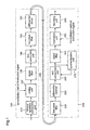
- Figure 1 is a block diagram illustrating a structure of a digital data transmission apparatus according to the first embodiment.
- the digital data transmission apparatus includes a transmitting end 100 for transmitting data, and a receiving end 200 for receiving the data transmitted from the transmitting end 100, which are connected with each other through a twisted pair cable 300.
- the transmitting end 100 includes a binary-to-quadrary conversion unit 110 for converting a 1-bit data stream into a 2-bit (four-valued) data stream; a coding unit 120 for mapping 2-bit data that is obtained by the binary/quadrary conversion unit to a predetermined signal level to be coded; a digital filter 130 that allows a band of frequency components corresponding to half of a symbol rate to pass; a D/A conversion unit 140 for converting the 2-bit data that has passed through the digital filter 130 into an analog signal; a low-pass filter 150 for eliminating a high-band signal from the analog signal; and a differential driver 160 for converting the analog signal that has passed through the low-pass filter 150 into two signals having opposite polarities relative to a reference potential, and inputting the two signals to the twisted pair cable 300.
- a binary-to-quadrary conversion unit 110 for converting a 1-bit data stream into a 2-bit (four-valued) data stream
- a coding unit 120 for mapping 2-bit data that is obtained by the
- the receiving end 200 includes a low-pass filter 210 that eliminates noises outside the signal band of a transmission signal for both wires of the twisted pair cable 300; a differential receiver 220 for receiving a signal that has passed through the low-pass filter 210; an A/D conversion unit 230 for converting the received signal into a digital signal; a digital filter 240 that allows only a predetermined frequency band to pass; an evaluation unit 250 for evaluating the level of the received signal; a decoding unit 260 for decoding the signal level evaluated by the evaluation unit 250 into 2-bit receipt data; and a synchronization unit 270 for generating a clock that is employed at the A/D conversion.
- a low-pass filter 210 that eliminates noises outside the signal band of a transmission signal for both wires of the twisted pair cable 300
- a differential receiver 220 for receiving a signal that has passed through the low-pass filter 210
- an A/D conversion unit 230 for converting the received signal into a digital signal
- a digital filter 240 that allows
- a digital signal that is transmitted through the transmitting end 100 is initially inputted to the binary/quadrary conversion unit 110.
- the binary/quadrary conversion unit 110 converts a 1-bit data stream into a 2-bit (four-valued) data stream, i.e., "01”, "11", "00", or "10", and transmits the 2-bit data stream to the coding unit 120.
- the coding unit 120 performs a coding process by mapping the signal inputted from the binary/quadrary conversion unit 110 to a signal level that represents the value of the signal.
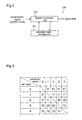
- This coding unit 120 includes, as shown in figure 2 , a previous value storage unit 121 for storing a previous value that is obtained by coding the immediately preceding data, and a signal conversion unit 122 for performing a coding process on the basis of the previous value that is stored in the previous value storage unit 121 and the signal outputted from the binary/quadrary conversion unit 110.
- the signal conversion unit 122 maps the signal to a signal level other than the level of the signal that has been coded immediately before, with reference to a conversion table as shown in figure 3 .
- the conversion table shown in figure 3 defines the signal levels to which the symbols to be transmitted, i.e. , "02", “11", “00”, or “10", are mapped on the basis of the previous signal level (0 to 4), so that the symbol is mapped to a signal level that is different from the previous level.
- the signal conversion unit 122 converts this symbol into a signal level "1”.
- the inputted signals are similarly mapped to four-value signal levels other than the respective previous signal levels.
- the coding unit 120 encodes the signal into a signal level that is different from the previous signal level in any case.
- Frequency components of the coded signal which are higher than half of the symbol rate, are eliminated by the digital filter 130.
- This digital filter 130 is a low-pass filter that allows a band of frequency components corresponding to half of the symbol rate to pass, and this digital filter is practically constructed so as to provide appropriate roll-off characteristics in conjunction with the digital filter 240 on the receiving end 200.
- the transmission of pulse signals requires an infinite bandwidth, but when the signal is passed through a filter having the roll-off characteristics, the signal is turned into a signal within a band that is slightly larger than half of the symbol rate, and converted into a signal without interference between adjacent codes in the reading timing. Accordingly, the data to be transmitted is converted into a signal in a limited band.
- the signal that has passed through the digital filter 130 is converted into an analog signal by the D/A conversion unit 140. That is, the signal is converted into a signal that includes a coded symbol in symbol timing of each symbol cycle. Folding frequency components of the analog signal, which appear in a band of frequencies that are twice as high as the frequencies that have passed through the digital filter 130 or higher frequencies, are eliminated by the low-pass filter 150, and the obtained signal is transmitted to the differential driver 160.
- the differential driver 160 converts the inputted signal into two signals having amplitudes which are proportional to the inputted signal and opposite polarities relative to a reference potential, and differentially outputs the obtained two signals to the twisted pair cable 300.
- the signal outputted from the differential driver 160 is a signal that is always coded so as to have a signal level different from the previous signal level, and this signal has values which constantly vary with symbol timing.
- the receiving end 200 makes the transmission signals which have been transmitted through both wires of the twisted pair cable 300 pass through the low-pass filter 210, to eliminate noises outside a predetermined signal band.
- the low-pass filter 210 cuts off components of an area in which the frequency characteristics of the receiver 220 cannot compensate for the desired characteristics, as well as converts the signal into a signal of a band which can be processed by the digital filter 240 that is connected in the later stage.
- the signal from which the noises have been eliminated by the low-pass filter 210 is received by the differential receiver 220.
- the differential receiver 220 outputs a signal which is proportional to a difference signal between the both wires of the twisted pair cable 300, and then the outputted signal is converted into a digital signal by the A/D conversion unit 230.
- the synchronization unit 270 generates a synchronized sampling clock and transmits the sampling clock to the A/D conversion unit 230, so that the A/D conversion unit 230 performs sampling in the symbol timing.
- the synchronization unit 270 includes a band pass filter 271, a D/A converter 272, a comparator 273, a PLL 274, and a frequency divider 275, as shown in an example of the construction of figure 7 .
- the frequency division rate of the frequency divider 275 is decided depending on how many times the sampling cycle is as high as the symbol cycle. For example, when the sampling rate is twice as high as the symbol rate, the frequency is divided by four.
- the synchronization unit 270 makes clock synchronization utilizing the signal levels of the received signal, which constantly vary with the symbol cycle.
- Frequency components corresponding to half of the symbol rate are extracted from the received signal by the band pass filter 271, then the signal is converted into an analog signal by the D/A converter 272, and the analog signal is converted into a square wave signal by the comparator 273.
- This square wave signal is inputted to the PLL 274 as a reference clock (REF), and phase comparison is performed between the reference clock and a clock (VAL) that is obtained by dividing the frequency of a clock outputted from the PLL 274 in the frequency divider 275, thereby establishing the clock synchronization. Consequently, the A/D conversion unit 230 samples the signal in the symbol timing, thereby to converts the analog signal into a digital signal.
- the structure of the synchronization unit 270 is not limited to that shown in figure 7 , and reproduction synchronization can be easily realized on the receiving end utilizing the fact that the values of other means also constantly vary with the symbol cycle.
- the obtained digital signal is passed through the digital filter 240.
- the digital filter 240 provides roll off characteristics in conjunction with the digital filter 130 on the transmitting end 100, and converts the passed digital signal into a signal that has no interference between adjacent codes and can be read in appropriate timing.
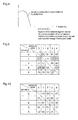
- the evaluation unit 250 evaluates the level of the signal that has been sampled in symbol timing, to decide a signal level from five-value levels. This evaluation process is carried out as shown in figure 4 , and the evaluation unit 250 evaluates the level of the sampled signal to decide one of signal levels 0, 1, 2, 3 and 4, on the basis of thresholds 1, 2, 3, and 4.
- the decoding unit 260 converts the signal level that has been evaluated by the evaluation unit 250 into 2-bit receipt data.
- This decoding unit 260 includes, as shown in figure 5 , a previous value storage unit 261 for storing a previous signal level that has been evaluated by the evaluation unit 250 in the immediately preceding symbol timing, and a signal conversion unit 262 for performing a decoding process on the basis of the signal level stored in the previous value storage unit 261 and the signal level outputted from the evaluation unit 250.
- the signal conversion unit 262 decodes the signal level into a symbol with reference to the conversion table shown in figure 6 .
- the conversion table in figure 6 is identical to the table that is employed at the coding by the coding unit 120 of the digital data transmission apparatus 100, and the receipt data is obtained with reference to the same conversion table as employed at the conversion in the digital data transmission apparatus 100.
- the signal conversion unit 262 converts the signal level into a symbol "10".
- CISPR25 defines a limitation value on the emitted noises for each frequency.
- a limitation value is defined for a frequency band of 30MHz or higher, in which the amount of emitted noises is relatively difficult to reduce.
- a limitation value for the emitted noises is defined also for a band of 30MHz or lower, while in this case it is possible to reduce the amount of noises by keeping balancing. Therefore, when the frequency band of the transmission signal is reduced to 30MHz or lower, the amount of emitted noises which complies with the on-vehicle requirements can be obtained.
- the twisted pair cable 300 has errors in the twisting pitch or the length of a wire connecting to the driver, and accordingly the transmission signal is slightly out of phase.
- the influence of the phase shifting gets larger as the frequencies of the signals to be transmitted are higher, and the signals do not cancel the emitted noises each other out.
- the digital filter performs a band limitation so that the signal bands of transmission signals are within the range of frequencies in which the emitted noises are sufficiently canceled each other out.
- Figure 8 is a diagram for explaining the relation between the noise elimination effect and the frequency level at the transmission through a twisted pair cable.
- the noise elimination effects of the twisted pair cable vary with the production precision, but the noise elimination effect is noticeably reduced when the frequency is beyond approximately 30MHz. Accordingly, the digital filter limits the signal band to below 30MHz.
- the digital filter 130 samples the signal at a frequency higher than the symbol rate. Then, the digital filter 130 sets frequency characteristics so that the combined characteristics of the digital filter 130 and the digital filter 240 have roll-off characteristics relative to half of the symbol rate, and the obtained characteristics are equally divided and given to the digital filters 130 and 240.
- a digital filter having such characteristics may be constituted by tens of FIR (FINITE IMPULSE RESPONSE) digital filters having coefficients.
- the digital filters 130 and 240 are low-pass filters that allow frequencies up to a level slightly higher than half of the symbol rate, to pass.
- signals having opposite polarities of a frequency band that is slightly higher than half of the symbol rate (which are accurately calculated on the basis of the rate of the roll-off characteristics, i.e., the percentage) are transmitted through the twisted pair cable 300. Then, the signals having opposite polarities are passed through two transmission wires of the twisted pair cable 300, then cancel the electromagnetic waves emitted therefrom each other out, resulting in almost no noise emission.
- the number of bits transmitted per symbol is set at 2 bits, and the symbol rate in this case is 24MHz.
- the roll off filter that is constituted by the digital filters 130 and 240 includes the roll off characteristics of approximately 15% relative to 12MHz, the signal band can be limited to approximately 15MHz.
- Such characteristics are realized by utilizing characteristics of a digital filter that enables to flexibly design frequency characteristics or phase characteristics and can realize steep frequency characteristics with ideal phase characteristics, thereby to limit a band of the data to a frequency band of the twisted pair cable having the noise elimination effect.
- the multi-valued transmission enables to lower the symbol rate, thereby realizing a higher transmission rate.
- the digital data transmission apparatus and the transmission channel coding method and decoding method of the first embodiment signal levels which are more than the number of symbols to be transmitted are provided, and the signal level representing each symbol in each symbol transmission timing is mapped to a signal level other than the signal level that was transmitted in the previous symbol timing.
- the signal can be converted into a signal level that is different from the previous signal level and, accordingly, the signals outputted from the transmitting end 100 always have values varying with the symbol cycle, thereby facilitating the synchronization on the receiving end 200.
- the signal level that represents a symbol is transmitted each time the symbol is coded, thereby realizing the data transmission with little delay.
- the digital filter 130 and the digital filter 240 constitute a filter having appropriate roll off characteristics, whereby the signal that has passed through the filters is converted into a signal within a frequency band that is slightly larger than half of the symbol rate. Further, the signal is converted into a signal without interference between adjacent codes in predetermined timing, so that a code included in the signal can be read in predetermined timing.
- the coding unit 120 converts a signal into a symbol that enables transmission of data comprising 2 or more bits per symbol timing, whereby efficient data transmission can be performed in a limited frequency band.
- the previous signal level is stored in the previous value storage unit 121, and the signal conversion unit 122 encodes a symbol to be transmitted on the basis of the previous signal level. Therefore, the signal can be mapped to a signal level other than the signal level which was transmitted in the previous symbol timing, whereby the signal is converted into a signal level that is different from the previous signal level in any case.
- the decoding unit 260 the previous signal level is stored in the previous value storage unit 261, and the signal conversion unit 262 decodes the received signal level on the basis of the previous signal level, whereby the transmitted symbol is obtained from the received signal level. In addition, a symbol that is represented by a signal level is obtained each time the signal level is received, thereby realizing the data receipt with little delay.
- 2-bit data is transmitted per symbol and the number of symbols to be transmitted is set at four, so that efficient data transmission is performed in a limited band.
- signal levels which are one more than the number of symbols to be transmitted are provided, so that the previous signal level is prohibited and the symbol to be transmitted is mapped to the signal level other than the previous value, whereby continuous outputs of the same signal level is avoided.
- the symbols to be transmitted are mapped to the signal levels in the order of "01”, “11", “00”, and “10” starting from the lowest signal level, so that the symbols can be mapped to the corresponding predetermined signal levels.
- the symbols are made correspond to the respective signal levels other than the previous signal level on the basis of the signal level of the immediately preceding detected signal, to decode the detected signal level into a symbol, whereby the transmitted symbol can be obtained from the received signal level. Further, a symbol that is represented by a signal level can be obtained each time the signal level is received, thereby realizing the data receipt with little delay.
- the synchronization unit 270 extracts, from a receipt signal, frequency components having a cycle that is half of the symbol cycle signal, and controls the symbol extraction timing on the basis of the phase of the extracted signal, whereby a more reliable synchronization can be established utilizing changes in the signal level of the receipt signal.
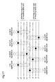
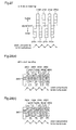
- FIG. 9 is a diagram showing possible values in the case where the signals are coded by the bi-phase mark method. In this figure, symbols other than circled and boxed symbols will not be coded. Values which can be taken in each symbol timing are binary, and the distance between adjacent symbols is 2 or more symbols across the signal level 2.
- a transmission method instruction signal is inputted to the coding unit 120 and the evaluation unit 250, to switch between a case of transmitting simply a bit string and a case of transmitting the data that has been coded by the bi-phase mark method.
- the coding unit 120 encodes an inputted symbol with referring to the conversion table shown in figure 9 .
- the evaluation unit 250 decides whether a received signal is higher or lower than threshold 5 shown in figure 4 .
- the previous signal level is 0, and when the received signal is higher than the threshold 5 the signal level of the received signal is set at 3, while the signal level is set at 1 when the received signal is lower than the threshold 5.
- the previous signal level is 1 and when the received signal is higher than the threshold 5 the signal level of the received signal is set at 3, while the signal level is set at 0 when the received signal is lower than the threshold 5.
- the previous signal level is 3, and when the received signal is higher than the threshold 5 the signal level of the received signal is set at 4, while the signal level is set at 1 when the received signal is lower than the threshold 5.
- the previous signal level is 4, and when the received signal is higher than the threshold 5 the signal level of the received signal is set at 3, while the signal level is set at 1 when the received signal is lower than the threshold 5.
- the transmission/receipt of data which have been coded according to the bi-phase mark method can realize resistance to noises that is quite close to the binary transmission.
- a threshold at the threshold evaluation with the previous signal level and the signal level of the received signal is set at threshold 5, and the symbol can be decoded by evaluating the signal only by deciding whether it is higher or lower than a threshold, like in the binary transmission, thereby realizing signal detection having a reliability that is quite close to the binary evaluation.
- possible values taken in each symbol timing are binary, and the distance between symbols is two or more symbols across the signal level 2, so that the possibility of errors caused by noises can be suppressed to a level as low as the binary transmission.
- the four-value symbol is converted into five-value signal levels, while also in cases where the four-value symbol is converted into multi-value signal levels which are more than four, such as 8-value or 16-value, the similar method is used to prevent a code from being mapped to the signal level of the immediately preceding signal, and accordingly the same effects are obtained.
- the coding by the coding unit 120 is performed with reference to the conversion table as shown in figure 3 , while the coding is not restricted to this method, but the coding can be performed with reference to a conversion table as shown in figure 10 .
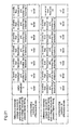
- the conversion table shown in figure 10 defines signal levels to which symbols to be transmitted are mapped, on the basis of a difference in signal level from the previous signal level corresponding to the immediately preceding transmitted signal. More specifically, when a symbol "10" is transmitted, this symbol is mapped to a signal level that is larger than the previous signal level by one level, or a signal level smaller than the previous signal level by four levels. Similarly, a symbol “00” is mapped to a signal level that is larger than the previous signal level by two levels, or a signal level smaller than the previous signal level by three levels. A symbol “11” is mapped to a signal level that is larger than the previous signal level by three levels, or a signal level smaller than the previous signal level by two levels. A symbol “01” is mapped to a signal level that is larger than the previous signal level by four levels, or a signal level smaller than the previous signal level by one level.
- the evaluation unit 250 detects a difference from the previous signal level corresponding to the immediately preceding received signal, thereby to obtain a symbol. More specifically, the previous signal level is stored, then a difference between the stored signal level and the received signal level is obtained, and the obtained difference is evaluated on the basis of thresholds 1 to 7 as shown in figure 11 , thereby to assigning one of signal evaluation values "-4" to "+4" to the received signal. Then, the obtained signal evaluation value is transmitted to the decoding unit 260.
- the decoding unit 260 decodes the signal evaluation values "-4", “-3", “-2”, “-1”, “+1”, “+2”, “+3”, and "+4" into symbols "01”, "11”, "00”, “10”, “01”, “11”, “00”, and "10”, respectively.
- the symbol of the transmitted signal can be decided only on the basis of the difference in signal level from the previous signal, so that for example when the transmitting end 100 and the receiving end 200 have different potentials or the potentials vary, and even when the absolute voltage level cannot be detected on the transmitting end 100, the data can be correctly decoded by detecting the difference from the immediately preceding received signal level.
- the transmitting end 100 always maps a symbol to a signal level other than the previous signal level and transmits the obtained symbol, so that the voltages constantly vary with symbol. Therefore, it is satisfactory that the receiving end 200 detects alternating components (the voltage fluctuation level), and when the potential difference between the transmitting end 100 and the receiving end 200 is quite large, a circuit for cutting off the alternating components can be provided in the receiving end. This is useful in circumstances where the transmitting end and the receiving end have different ground levels or where the voltage-resistant characteristics are demanded, such as in a case where the apparatus is mounted on a motor vehicle.
- data which has been coded by the bi-phase mark method may be mapped to a signal level with referring to the conversion table shown in figure 10 .
- the distance between symbols is always two ore more levels, so that the evaluation is performed by setting a threshold at an intermediate signal level between respective possible symbols, thereby to realize the data receipt with higher precision.
- Another conversion table may be employed so long as symbols are mapped on the basis of a difference between the previous signal level and the next assumable signal level.
- the evaluation unit 250 When a signal level that has been coded on the basis of the signal level difference is received and decoded, the evaluation unit 250 may be constructed as shown in figure 12.
- Figure 12 is a block diagram illustrating another construction of the evaluation unit 250.
- This evaluation unit 250 includes a threshold evaluation unit 251 that holds a threshold and subjects a signal that has passed through the digital filter 240 to threshold evaluation, a threshold control unit 252 that controls the threshold, and a previous value storage unit 253 that stores the immediately preceding signal level.
- the threshold evaluation unit 251 calculates a difference between the signal level of a signal that has passed through the digital filter 240 and the previous signal level that is stored in the previous value storage unit 253, and evaluates the obtained difference on the basis of thresholds 1 to 7 as shown in figure 11 , thereby assigning one of signal evaluation values "-4" to "+4" to the signal. Then, the variation in the signal level (signal evaluation value) is transmitted to the decoding unit 260, as well as the present signal level is stored in the previous value storage unit 253, and the difference between the signal evaluation value (evaluation result) and the previous signal level is transmitted to the threshold control unit 252. Then, the threshold control unit 252 calculates differences corresponding to one fluctuation in the threshold, on the basis of the received difference and the signal evaluation value.
- the threshold evaluation unit 251 changes the threshold in accordance with the threshold evaluation signal.
- the threshold is modified on the basis of the evaluation result on the signals that have been received for a predetermined period. Accordingly, in cases where the transmitted voltage varies according to the change in the supply voltage or the like, correct data can be obtained by modifying the threshold.
- the evaluation unit 250 when modifying the threshold, obtains differences corresponding to one variation in the threshold to obtain an average.
- any value such as a value corresponding to the maximum amplitude may be obtained so long as this value enables to modify changes in the amplitude level in the signal waveform which has been transmitted from the transmitting end 100, and the threshold can be appropriately modified by averaging such values during a predetermined period.
- the modification of the threshold is performed after the processing by the digital filter is performed, while the threshold may be fixed and the received signal is amplified to change the amplitude into an appropriate level.
- signal levels which are one more than the number of symbols are provided, then a signal level of a signal that was transmitted in the previous symbol timing is employed as a prohibit level, and the symbol is mapped to other signal level.
- the number of signal levels may be increased, thereby to increase the number of prohibit levels. For example, increase or decrease of the previous signal level with relative to a signal level that is antecedent to the previous signal level is stored and, when the signal level is dropping, signal levels which are lower than the previous signal level are prohibited in the next symbol timing. On the other hand, when the signal level is rising, signal levels which are higher than the previous signal level are prohibited.
- the signal waveform in this case constantly rises and drops repeatedly in each symbol timing, whereby a synchronization clock having a stable phase is generated on the receiving end.
- modulation such as ASK (amplitude shift keying) or 64QAM (Quadrature Amplitude Modulation) is performed.
- signal bands are located on both sides of the modulation frequency, so that the frequency required for each symbol rate at the baseband transmission is reduced to half, whereby the limited band due to the characteristics of the twisted pair cable is effectively utilized, resulting in higher-speed transmission.
- the phase and amplitude are both subjected to the modulation like in 64QAM, more efficient transmission can be performed, thereby realizing a higher transmission rate also when the same twisted pair cable is employed.
- a digital data transmission apparatus as defined in any of Claims 1 to 4, 7 to 9, and 11 to 13 of the present invention, a transmission channel coding method as defined in any of Claims 19, 21 to 24, 26 and 27, and a decoding method as defined in Claim 31 will be described as a second embodiment, with
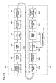
- Figure 13 is a block diagram illustrating a digital data transmission apparatus according to the second embodiment of the present invention.
- the same or corresponding elements as those in figure 1 are denoted by the same reference numerals, and will not described in detail herein.
- a transmitting end 400 of the digital data transmission apparatus consists of a serial-to-parallel conversion unit 410 for grouping a received data stream, 2 bits by 2 bits, to be converted into four-value symbols; a coding unit 410 for coding a symbol into any of eight-value signal levels; a digital filter 130 that allows a band of frequency components corresponding to half of the symbol rate to pass; a D/A conversion unit 140 for converting 2-bit data that has passed through the digital filter 130 into an analog signal; a low-pass filter 150 for eliminating a high-band signal from the analog signal; and a differential driver 160 for amplifying the signal that has passed through the low-pass filter so as to have sufficient signal strength to be transmitted to the twisted pair cable 300 (transmission channel) and differentially outputting the obtained signals.
- the receiving end 500 consists of a low-pass filter 210 for eliminating noises outside of a signal band of a transmission signal from both wires of the twisted pair cable 300; a differential receiver 220 for receiving a signal that has passed through the low-pass filter 210; an A/D conversion unit 230 for converting the received signal into a digital signal; a digital filter 240 that allows only a predetermined frequency band to pass; a decoding unit 510 for evaluating a symbol represented by the level of the received signal; a parallel-to-serial conversion unit 520 for converting a symbol into 2-bit serial data; and a synchronization unit 270 for generating a clock that is employed at the A/D conversion of the received signal.
- a digital signal to be transmitted through the transmitting end 400 is initially inputted to the serial/parallel conversion unit 410.
- the serial/parallel conversion unit 410 groups the received data stream, 2 bits by 2 bits, and converts the data into four-value symbols, i.e., "00", "01", “10", and “11", to be transmitted to the coding unit 420.
- the coding unit 420 maps the received signal into one of eight-value signal levels, i.e., "-7", “-5", “-3”, “-1", “+1”, “+3", “+5", and "+7", to be coded.
- Frequency components higher than half of the symbol rate, of the signal that has been converted into the signal level by the coding unit 420 are eliminated by the digital filter 130, and the obtained signal is converted into an analog signal by the D/A conversion unit 140.
- the obtained analog signal is a signal that includes a coded symbol at symbol timing of each symbol cycle.
- the high-band signal of the analog signal is eliminated by the low-pass filter 150, and the obtained signal is transmitted to the differential driver 160.
- the differential driver 160 converts this signal into two signals having amplitudes which are proportional to the inputted signal and having opposite polarities relative to a reference potential, and differentially outputs the two signals to the twisted pair cable 300.
- the signals outputted from the differential drivers 160 have been coded so as to always take signal levels that are different from the previous signal levels, and the values of the signals constantly vary with symbol timing.
- the transmission signals transmitted through both wires of the twisted pair cable 300 are passed through the low-pass filter 210 to eliminate noises outside a predetermined signal band, and the obtained signal is received by the differential receiver 220. Then, this signal is converted into a digital signal by the A/D conversion unit 230.
- the synchronization unit 270 generates a synchronized sampling clock, utilizing the fact that values of the transmission signal are constantly increased or decreased with symbol cycles so that the A/D conversion unit 230 samples the signal in symbol timing, and then transmits the generated clock to the A/D conversion unit 230.
- the A/D conversion unit 230 samples the received signal in symbol timing of the sampling clock generated by the synchronization unit 270, to be converted into a digital signal.
- the obtained digital signal is passed through the digital filter 240, to be converted into a signal that has no interference between adjacent codes and can be read in appropriate timing.
- the decoding unit 510 evaluates the signal level of the signal that has been obtained by the sampling in symbol timing to decide which symbol among "00", "01", "10", and "11” is represented by the signal level, thereby decoding the received signal into a symbol.
- the parallel/serial conversion unit 520 converts the received symbol into 2-bit serial data, and outputs the same sequence of digital signal as that of the digital signal inputted to the serial/parallel conversion unit 410 on the transmitting end 400.
- the coding unit 420 is initially described.
- Figure 14 is a block diagram illustrating a structure of the coding unit 420.
- the coding unit 420 includes a previous signal level storage unit 421 that stores the previous signal level that was coded immediately before; a mapping table 422 that defines signal levels to which the symbols to be transmitted, i.e., "01", “11", “00", and “10” are mapped on the basis of the previous signal level; and a signal conversion unit 423 for carrying out a coding process with referring to the mapping table 422, on the basis of the value that is stored in the previous signal level storage unit 421 and the signal inputted from the serial/parallel conversion unit 410.
- the initial value of the previous signal level storage unit 421 may be any signal level so long as this signal level can be transmitted to the digital filter 130.
- the mapping table 422 includes signal levels which are twice as many as the number of symbols, as specifically shown in figure 15 .
- the symbols to be transmitted are mapped alternately to one of upper half signal levels and one of lower half signal levels in each symbol cycle, and the signal level to be transmitted is decided on the basis of the received symbol and the previous signal level.
- the signal conversion unit 423 decides the signal level to be transmitted with referring to the mapping table 422 on the basis of two values, i.e., the symbol that is received from the serial/parallel conversion unit 410 and the previous signal level that is stored in the previous signal level storage unit 421, and transmits the decided signal level to the digital filter 130.
- the previous signal level storage unit 421 destroys the signal level that has been held, thereby to newly hold the signal level that has been received this time, for the coding in the next symbol timing.
- the signal level "-1" is stored in the previous signal level storage unit 421 at a time when n-th symbol "00" is received.
- the signal conversion unit 423 refers to the mapping table 422, to decide a signal level to be transmitted at "+7", on the basis of two values, i.e., the received symbol "00" and the previous signal level "-1", and transmits the obtained signal level to the digital filter 130.
- the previous signal level storage unit 421 changes the stored previous signal level to "+7".
- the signal conversion unit 423 receives (n+1)-th symbol "10" in the next symbol timing, and decides a signal level to be transmitted at "-3 with reference to the mapping table 422 on the basis of the received symbol "10" and the previous signal level "+7", to be transmitted to the digital filter 130.
- the previous signal level storage unit 421 changes the stored the signal level to "-3".
- the signal conversion unit 423 decides the signal levels to be transmitted at "+1", "-5”, “+7", “-7” and "+7", successively from the (n+2)-th received symbol, with reference to the mapping table 422.
- the signal levels transmitted to the digital filter 130 adaptively to the (n-1)-th to (n+6)-th symbols are mapped alternately to the upper half signal levels and the lower half signal levels as shown in figure 17 , and clock components are multiplexed thereto.
- Figure 18 is a block diagram illustrating a structure of the decoding unit 510.
- the decoding unit 510 includes a previous voltage holding unit 511 for holding a voltage corresponding to a signal level that was received in the previous symbol timing; a signal level difference evaluation unit 512 for evaluating a difference between the received signal level and the signal level that was received in the previous symbol timing; a signal level difference threshold holding unit 513 that holds a threshold for the evaluation of the signal level difference in the signal level difference evaluation unit 512; a signal conversion unit 514 for evaluating a symbol represented by the received signal level, thereby to be decoded; and an inverse mapping table 515 that is referred to by the signal conversion unit 514 at the decoding.
- the signal level difference threshold holding unit 513 initializes or updates the held value in any timing.
- the transmitting end 400 alternately transmits the signal mapped to the signal level "+7" and the signal mapped to the signal level "-7", and then the receiving end 500 receives the respective signals to obtain a difference of voltages corresponding to the levels of the received signals.
- the obtained difference is a difference in actual voltage in the case where the difference in signal level is ⁇ 7 levels.
- a threshold voltage is calculated on the basis of the difference in voltage to know the number of levels corresponding to change of the signal from the previous symbol timing in each symbol timing, and then each calculated value is held.
- a voltage corresponding to each threshold is calculated with assuming that the signal level varies by +7 levels when the voltage varies by +28.
- the update of the value held in the signal level difference threshold holding unit 513 is carried out in the following way: for example, the signal level of the received signal is evaluated in each symbol timing on the basis of the held threshold, then an error, i.e., a difference between the threshold voltage value that is presently held adaptively to the signal level and the voltage value corresponding to the signal level that is received in the present symbol timing is detected, and the threshold is modified on the basis of the detected error.
- the initialization and update in the signal level difference threshold holding unit 513 are carried out as described above, but any method may be employed so long as the threshold for evaluating the number of difference levels corresponding to a difference in voltage between the received signal level and the signal level in the previous symbol timing can be acquired.
- the signal level difference evaluation unit 512 calculates a difference between the voltage of the received signal level and the voltage held in the previous voltage holding unit 511, and selects a threshold corresponding to the calculated difference from thresholds which are held in the signal level difference threshold holding unit 513. Then, the number of difference levels corresponding to the selected threshold is evaluated as shown in a table of figure 21 , and then the number of difference levels is transmitted to the signal conversion unit 514.
- the signal conversion unit 514 evaluates a symbol represented by the received signal level, with reference to the inverse mapping table 515 on the basis of the signal level difference evaluated by the signal level difference evaluation unit 512.
- the inverse mapping table 515 defines symbols corresponding to the numbers of difference levels, as specifically shown in figure 22 . The obtained symbol is transmitted to the parallel/serial conversion unit 520 and the previous voltage holding unit 511.
- the previous voltage holding unit 511 When receiving a new signal level, the previous voltage holding unit 511 destroys the previous voltage that has been held, and holds the voltage corresponding to the received signal level to be updated.
- the digital data transmission apparatus, and the transmission channel coding method and the decoding method according to the second embodiment provides signal levels which are twice as many as the number of symbols to be transmitted, and encodes a signal level that represents each symbol in each symbol timing, by being mapped to one of signal levels other than the signal level that was transmitted in the previous symbol timing. Therefore, the symbol can be converted into a signal level other than the previous signal level, whereby values of the signals outputted from the transmitting end constantly vary with symbol timing, and synchronization in symbol timing on the receiving end 500 can be readily established.
- the symbol to be transmitted is alternately mapped to a lower half signal level and an upper half signal level in each symbol cycle, whereby the mapping in which the signal level is constantly increased or decreased in symbol timing can be performed. Consequently, the frequency components corresponding to half of the symbol rate are contained in the transmission signal to multiplex the clock components therein, whereby the reproduction synchronization can be readily established on the receiving end 500.
- the difference in signal level from the previous signal can be calculated and simultaneously the symbol can be obtained, thereby realizing signal transmission with little delay.
- the symbol information is included in the difference between the signal level received in the previous symbol timing and the signal level received in the present symbol timing.
- the absolute voltage level on the transmitting end 400 cannot be detected, for example, in cases where the transmitting end 400 and the receiving end 500 have different potentials or where the potentials vary, data can be transmitted correctly.
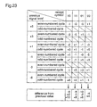
- mapping table as shown in figure 23 is employed as the mapping table 422 of the coding unit 420.
- the mapping table in figure 23 defines signal levels that are 1.5 times as many as the number of symbols.
- the symbols to be transmitted to are mapped alternately to one of signal levels which are as many as the number of kinds of the symbols beginning from the lowest signal level in even-numbered symbol cycles, and one of signal levels which are as many as the number of the kinds of the symbols beginning from the highest signal level in odd-numbered symbol cycles.
- the signal levels to be transmitted are decided on the basis of the received signal and the previous signal level.
- mapping table 422 as shown in figure 15 is employed at the coding
- the inverse mapping table as shown in figure 22 is employed at the decoding.
- any mapping table may be employed so long as the mapping table enables to multiplex the clock components so that the reproduction synchronization is readily established, and map the symbols to the differences between the previous signal level and the signal level to be transmitted.
- the symbols are mapped to the difference between the previous signal level and the signal level to be transmitted, while the absolute value of the signal level, which is defined for each symbol, may be employed to map four symbols to eight signal levels as shown in figure 24 . Further, four symbols can be mapped to six signal levels as shown in figure 25 . In these cases, when the absolute voltage level on the transmitting end can be detected, the same effect as described in this second embodiment is achieved.
- a digital data transmission apparatus as defined in Claim 15 and a transmission channel coding method as defined in Claim 28 or 29 will be described as a third embodiment of the present invention, with reference to the drawings.
- Figure 26 is a block diagram illustrating structures of a transmitting end 600 and a receiving end 700 according to the third embodiment.
- the same or corresponding elements as those in figure 13 are denoted by the same reference numerals and will not described in detail herein.
- the digital data transmission apparatus further includes a scrambler 610 for scrambling digital data to be transmitted and inputting the scrambled data to the serial/parallel conversion unit 410 in the transmitting end 400 according to the second embodiment, and a descrambler 710 for descrambling received data in the receiving end 500.
- Mapping on the transmitting end 600 according to the third embodiment is similar to the mapping on the transmitting end 400 according to the second embodiment. More specifically, the symbols are alternately mapped to signal levels which are as many as the number of kinds of the symbols starting from the lowest signal level, and signal levels which are as many as the number of kinds of the symbols starting from the highest signal level.
- Figure 27 shows an example in which four-value symbols are mapped to eight-value signal levels.
- signal levels 2701 and 2702 show signal levels to which symbols may be mapped in each symbol cycle.
- the symbols are always mapped so that one of lower four signal levels 2701 and one of upper four signal levels 2702 are alternately employed, thereby multiplexing clock components into a transmission signal with reliability.
- the symbols are mapped to signal levels which are less than twice as many as the number of kinds of the symbols, there are some cases where the clock components cannot be multiplexed into the transmission signal.
- Figures 28 show cases where four-value symbols are mapped to five-value signal levels.
- a signal level 2801 shows a signal level to which a symbol was mapped in the immediately preceding symbol cycle.
- Signal levels 2802 to 2805 show signal levels to which symbols may be mapped in the respective symbol cycles.
- the symbols are always mapped to the same signal level, and thus the clock components are not at all multiplexed into the transmission signal.
- digital data to be transmitted includes succession of "1" as shown in figure 28(b)
- clock components having the reverse phase to the intended clock components will be multiplexed.
- clock component are not multiplexed into a transmission signal like in these cases, synchronization of the clock cannot be established by the clock reproduction unit, whereby the A/D conversion unit 230 cannot sample the received signal, and thus the received signal may not be decoded.
- the scrambling is performed to multiplex clock components into the transmission signal.
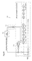
- Figure 29 illustrates a structure of the scrambler 610.
- the scrambler 610 multiplies digital data to be transmitted by data that is generated from the transmission data, thereby performing scrambling.
- a first arithmetic unit 611 extracts predetermined data and data that is antecedent to the predetermined data by four bits, from a scrambled data stream, and detects whether or not these two pieces of data coincide with each other.
- a [X]bit counter 612 is incremented by [1].
- the value of the [X]bit counter 612 is set at [0].
- a coincidence detection signal is outputted to a second arithmetic unit 613.
- Process A arithmetic is performed like in a process for inverting data when the coincidence signal is in a predetermined state, to change an array of the data to be transmitted, thereby performing scrambling.
- Figure 30 illustrates a structure of a descrambler 710 for descrambling the data that has been scrambled as described above.
- a first arithmetic unit 711 extracts prescribed data and data that is antecedent to the prescribed data by 4 bits, from a descrambled data stream, and detects whether these two pieces of data coincide with each other.
- a [X]bit counter 712 is incremented by [1].
- the value of the [X]bit counter 712 is set at [0].
- a coincidence detection signal is outputted to a second arithmetic unit 713.
- arithmetic is performed like in a process for inverting data when the coincidence signal is in a prescribed state, thereby descrambling the received data.
- the digital data to be transmitted is scrambled, whereby succession of the same value in the data to be transmitted can be prevented, and clock components can be multiplexed into the data to be transmitted.
- data to be transmitted and data that is antecedent to the data by 4 bits are extracted from the data stream to be transmitted, and the data is inverted to be scrambled when portions each including the two pieces of data that coincide with each other successively appear, whereby the clock components can be multiplexed into the transmission signal with reliability.
- the descrambling can be carried out without adjusting timing on the transmitting end and the receiving end, whereby any kind of data can be transmitted or received.
- the scrambler 610 performs the operation on the basis of the data T(-3) that was processed 3 bits before, and the data T(-20) that was processed 20 bits before, while this embodiment is not limited to these data but the same effect is achieved also when any data are operated.
- the descrambler 710 performs the operation on the basis of the data T(-3) that was processed 3 bits before and the data T(-20) that was processed 20 bits before, while this embodiment is not limited to these data but the same effect is achieved also when any data are operated.
- a digital data transmission/receiving apparatus as defined in Claim 18 of the present invention will be described as a fourth embodiment, with reference to the drawings.
- Figure 31 is a block diagram illustrating a structure of the digital data transmission/receiving apparatus according to the fourth embodiment.
- the digital data transmission/receiving apparatus consists of a transmission/receiving control unit 1300 for controlling transmission or receiving of data; and a data transmission/receiving unit 1400 for transmitting or receiving data.
- the data transmission/receiving unit 1400 includes the transmitting end 100 and the receiving end 200 of the digital data transmission apparatus as shown in figure 1 , which are not connected with each other. More specifically, the data transmission/receiving unit 1400 consists of a binary/quadrary conversion unit 1401; a coding unit 1402; a digital filter 1403; a D/A conversion unit 1404; a low-pass filter 1405; a driver 7.406; a low-pass filter 1407; a receiver 1408; an A/D conversion unit 1409; a digital filter 1410; an evaluation unit 1411; a decoding unit 1412; and a synchronization unit 1413.
- the transmission/receiving control unit 1300 judges whether data that has been received by the data transmission/receiving unit 1400 is to be retransmitted or not, and inputs data that is to be retransmitted into the binary/quadrary conversion unit 1401 of the data transmission/receiving unit 1400, while outputting data that will not be retransmitted to the outside as received data.
- the transmission/receiving unit 1300 multiplexes transmission data that is inputted from the outside into the data to be retransmitted, to transmit the multiplexed data to the data transmission/receiving unit 1400, and the data transmission/receiving unit 1400 transmits the received data.
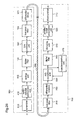
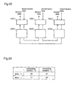
- Figure 32 shows an example where a plurality of the digital data transmission/receiving apparatus are connected in the form of a ring via buses.
- numerals 1501, 1502, and 1503 each denote a transmission/receiving control unit having the same construction as the transmission/receiving control unit 1300 in figure 31 .
- Numerals 1504, 1505, and 1506 each denote a data transmission/receiving unit having the same construction as the data transmission/receiving unit 1400 in figure 31 .
- transmission/receiving units are connected so that transmission data that is transmitted from a data transmission/receiving unit in the previous stage is received by a data transmission unit in the next stage, and transmission data that is transmitted from a data transmission/receiving unit in the last stage is received by the data transmission/receiving unit in the first stage.
- Each of the transmission/receiving control units 1501 to 1503 performs processing of upper communication layers, such as address management.
- Each of the data transmission/receiving units 1504 to 1506 exchanges data among the transmission/receiving control units 1501 to 1503.
- the present invention provides a digital data transmission apparatus, a transmission channel coding method, and a decoding method, by which digital data are converted into multi levels and coded so as not to take the same signal level successively, thereby realizing high-speed data transmission, as well as noise emission in a band of 30MHz or lower is reduced by a digital filter up to the amount that is compliant with requirements for mounting on motor vehicles.
Landscapes
- Engineering & Computer Science (AREA)
- Computer Networks & Wireless Communication (AREA)
- Signal Processing (AREA)
- Power Engineering (AREA)
- Physics & Mathematics (AREA)
- Spectroscopy & Molecular Physics (AREA)
- Dc Digital Transmission (AREA)
- Burglar Alarm Systems (AREA)
- Radar Systems Or Details Thereof (AREA)
- Reduction Or Emphasis Of Bandwidth Of Signals (AREA)
- Communication Control (AREA)
- Compression, Expansion, Code Conversion, And Decoders (AREA)
- Synchronisation In Digital Transmission Systems (AREA)
Claims (5)
- System, aufweisend eine Sendevorrichtung und eine Empfangsvorrichtung, zum Empfangen von digitalen Daten, die von einer Sendevorrichtung gesendet worden sind,
wobei die Sendevorrichtung Folgendes aufweist:Datencodierungsmittel (110, 120) zum (i) Umwandeln von digitalen Daten, die während jeder von mehreren aufeinander folgenden Symbolperioden ankommen, in einen entsprechenden Symbolwert, der die digitalen Daten für die Dauer der entsprechenden Symbolperiode darstellt, und (ii) Umwandeln des Symbolwerts in einen Signalpegel, wobei die Datencodierungsmittel so betreibbar sind, dass es zu einer Änderung des Signalpegels zwischen aufeinander folgenden Symbolperioden unabhängig davon kommt, ob sich die digitalen Daten ändern oder nicht;ein erstes digitales Filter (130), das so konfiguriert ist, dass es mit einer ersten Abtastperiode, die kürzer als die Symbolperiode ist, arbeitet und nur festgelegte Frequenzen des Ausgangssignals von den Datencodierungsmitteln durchlässt;D/A-Umwandlungsmittel (140) zum Umwandeln des Digitaldatenstroms, der das erste digitale Filter (130) passiert hat, in ein analoges Signal;ein Tiefpassfilter (150) zum Eliminieren, aus dem mit den D/A-Umwandlungsmitteln (140) erhaltenen analogen Signal, von Frequenzen, die mindestens doppelt so hoch wie die Frequenzen sind, die das erste digitale Filter (130) passiert haben; undeinen Differenzialtreiber (160) zum Umwandeln eines Ausgangssignals des Tiefpassfilters (150) in zwei Signale, die in Bezug auf ein vorgegebenes Referenzpotenzial entgegengesetzte Polaritäten aufweisen, und Eingeben der zwei Signale in ein verdrilltes Twisted-Pair-Kabel (300);wobei das erste digitale Filter (130) Frequenzeigenschaften zum Abschalten von mindestens der Frequenzkomponenten hat, die höher sind als ein Frequenzband, in dem die von den jeweiligen Signalen ausgegebenen elektromagnetischen Wellen, die durch das Twisted-Pair-Kabel passieren, einander aufheben,wobei die Empfangsvorrichtung Folgendes aufweist:einen Differenzialempfänger (220) zum Empfangen von durch ein Twisted-Pair-Kabel gesendeten Sendesignalen und Umwandeln einer Differenz der Potenziale zwischen zwei Adern des Kabels in ein Signal;A/D-Umwandlungsmittel (230) zum Umwandeln des vom Differenzialempfänger (220) ausgegebenen Signals in einen digitalen Signalwert, wobei die A/D-Umwandlungsmittel konfiguriert sind für einen Betrieb in einer vorgegebenen Abtastperiode;ein zweites digitales Filter (240), das nur ein vorgegebenes Frequenzband eines digitalen Datenstroms, der durch Abtasten mit den A/D-Umwandlungsmitteln erhalten worden ist, passieren lässt; undein Pegelbeurteilungsmittel (250, 260; 510, 520) zum Beurteilen eines Symbolwerts anhand des Pegels des digitalen Signalwerts aufgrund des Ausgangssignals vom zweiten digitalen Filter (240) und zum Umwandeln des Symbolwerts in entsprechende digitale Daten,wobei das zweite digitale Filter (240) Tiefpass-Eigenschaften hat,wobei das zweite digitale Filter (240) solche Sendeeigenschaften aufweist, dass bei Anwendung in Kombination mit dem ersten digitalen Filter (130) die ersten und zweiten digitalen Filter (130, 240) zusammen Absenkeigenschaften für ein Signal zeigen, dass durch das erste digitale Filter (130) und das zweite digitale Filter (240) passiert, undwobei die Frequenzeigenschaften der ersten und zweiten digitalen Filter (130, 240) so festgelegt sind, dass die kombinierten Eigenschaften der ersten und zweiten digitalen Filter (130, 240) Absenkeigenschaften bezogen auf die Hälfte der Symbolrate haben. - System nach Anspruch 1, wobei
die Pegelbeurteilungsmittel Folgendes aufweisen:Signalpegelbeurteilungsmittel (251) zum Erkennen eines Signalpegels in jeder Symbolperiode; undMittel (253) zum Speichern des vorhergehenden Signalpegels, der in der unmittelbar vorhergehenden Empfangszeit empfangen worden war, unddie Pegelbeurteilungsmittel den von den Signalpegel-Erkennungsmitteln erkannten Signalpegel aufgrund des vorhergehenden Signalpegels, der in den Mitteln zum Speichern des vorhergehenden Signalpegels gespeichert ist, in ein entsprechendes Symbol decodieren. - System nach Anspruch 1 oder 2, wobei
die Pegelbeurteilungsmittel Folgendes aufweisen:Schwellenwert-Steuermittel (252) zum Korrigieren eines Beurteilungs-Schwellenwerts aufgrund von Änderungswerten bei entsprechenden Signalpegeln, die während einer vorgegebenen Periode empfangen wurden;Mittel (253) zum Speichern eines vorhergehenden Signalpegels, der einem Signal entspricht, das in der unmittelbar vorhergehenden Symbol-Empfangszeit empfangen wurde; undMittel (251) zum Durchführen einer Schwellenwert-Beurteilung durch Beurteilen einer Signalpegel-Differenz zwischen einem aktuellen Signalpegel und dem vorhergehenden Signalpegel, um dadurch einen Symbolwert zu decodieren. - System nach Anspruch 1 oder 3, wobei
die Pegelbeurteilungsmittel Synchronisationsmittel (270) zum Herstellen der Synchronisation mit einer Symbolperiode eines empfangenen Signals aufweisen, und
die Synchronisationsmittel (270) so betreibbar sind, dass sie aus dem empfangenen Signal Frequenzkomponenten extrahieren, die eine Periode haben, die doppelt so lang wie die Symbolperiode ist, und einen Zeitpunkt, zu dem ein Symbol erkannt wird, aufgrund einer Phase eines extrahierten Signals steuern. - System nach einem der Ansprüche 1 bis 4, wobei
die Pegelbeurteilungsmittel so betreibbar sind, dass sie in einem ersten Decodierungsmodus beliebige digitale Daten decodieren und in einem zweiten Decodierungsmodus, der von dem ersten Codierungsmodus verschieden ist, digitale Daten in Form von Daten ausgeben, die mit dem Zweiphasenmarkierungsverfahren codiert worden sind, und wobei die Pegelbeurteilungsmittel ein Übertragungsverfahren-Hinweis-Signal erhalten, das angibt, ob die in die Datencodierungsmittel eingegebenen digitalen Daten bereits mit dem Zweiphasenmarkierungsverfahren codiert worden sind oder nicht.
Applications Claiming Priority (4)
| Application Number | Priority Date | Filing Date | Title |
|---|---|---|---|
| JP2000305821 | 2000-10-05 | ||
| JP2001061322 | 2001-03-06 | ||
| JP2001061323 | 2001-03-06 | ||
| EP01974702A EP1331776B1 (de) | 2000-10-05 | 2001-10-05 | Digitaler datensender |
Related Parent Applications (1)
| Application Number | Title | Priority Date | Filing Date |
|---|---|---|---|
| EP01974702A Division EP1331776B1 (de) | 2000-10-05 | 2001-10-05 | Digitaler datensender |
Publications (2)
| Publication Number | Publication Date |
|---|---|
| EP1933512A1 EP1933512A1 (de) | 2008-06-18 |
| EP1933512B1 true EP1933512B1 (de) | 2015-08-12 |
Family
ID=27344870
Family Applications (2)
| Application Number | Title | Priority Date | Filing Date |
|---|---|---|---|
| EP08150945.7A Expired - Lifetime EP1933512B1 (de) | 2000-10-05 | 2001-10-05 | Vorrichtung zur Kodierung und Dekodierung |
| EP01974702A Expired - Lifetime EP1331776B1 (de) | 2000-10-05 | 2001-10-05 | Digitaler datensender |
Family Applications After (1)
| Application Number | Title | Priority Date | Filing Date |
|---|---|---|---|
| EP01974702A Expired - Lifetime EP1331776B1 (de) | 2000-10-05 | 2001-10-05 | Digitaler datensender |
Country Status (7)
| Country | Link |
|---|---|
| US (1) | US7190728B2 (de) |
| EP (2) | EP1933512B1 (de) |
| JP (1) | JP3502630B2 (de) |
| KR (1) | KR100544218B1 (de) |
| AT (1) | ATE427611T1 (de) |
| DE (1) | DE60138208D1 (de) |
| WO (1) | WO2002030075A1 (de) |
Families Citing this family (21)
| Publication number | Priority date | Publication date | Assignee | Title |
|---|---|---|---|---|
| JP2005175827A (ja) * | 2003-12-10 | 2005-06-30 | Matsushita Electric Ind Co Ltd | 通信装置 |
| WO2005074220A1 (ja) * | 2004-01-28 | 2005-08-11 | Matsushita Electric Industrial Co., Ltd. | データ送信装置、データ受信装置およびデータ伝送方法 |
| US20060034388A1 (en) * | 2004-01-28 | 2006-02-16 | Yuji Mizuguchi | Data sending device, data receiving device, transmission path encoding method, and decoding method |
| JP2006109026A (ja) * | 2004-10-05 | 2006-04-20 | Hitachi Ltd | 光信号通信装置 |
| FR2878097B1 (fr) * | 2004-11-16 | 2007-02-16 | Airbus France Sas | Detection d'erreurs dans les donnees concernant l'actionnement d'un organe de vehicule |
| JP4129050B2 (ja) | 2006-04-27 | 2008-07-30 | 松下電器産業株式会社 | 多重差動伝送システム |
| JP2008048239A (ja) * | 2006-08-18 | 2008-02-28 | Nec Electronics Corp | シンボルタイミング検出方法および装置並びにプリアンブル検出方法および装置 |
| KR100782791B1 (ko) * | 2006-08-31 | 2007-12-05 | 삼성전기주식회사 | 디지털 변조 회로 |
| JP4821788B2 (ja) * | 2008-03-06 | 2011-11-24 | 富士通株式会社 | リーダー装置、その装置の送信方法及びタグ |
| US8141784B2 (en) | 2009-09-25 | 2012-03-27 | Hand Held Products, Inc. | Encoded information reading terminal with user-configurable multi-protocol wireless communication interface |
| US20110116424A1 (en) * | 2009-11-19 | 2011-05-19 | Hand Held Products, Inc. | Network-agnostic encoded information reading terminal |
| EP2434648A1 (de) * | 2010-09-25 | 2012-03-28 | ATLAS Elektronik GmbH | Codierer und Decodierer, Codierverfahren und Decodierverfahren sowie System aus Codierer und Decodierer |
| WO2012157722A1 (ja) | 2011-05-18 | 2012-11-22 | シャープ株式会社 | 液晶表示装置 |
| US8779898B2 (en) | 2011-08-17 | 2014-07-15 | Hand Held Products, Inc. | Encoded information reading terminal with micro-electromechanical radio frequency front end |
| US10013588B2 (en) | 2011-08-17 | 2018-07-03 | Hand Held Products, Inc. | Encoded information reading terminal with multi-directional antenna |
| US8596533B2 (en) | 2011-08-17 | 2013-12-03 | Hand Held Products, Inc. | RFID devices using metamaterial antennas |
| JP2013251857A (ja) * | 2012-06-04 | 2013-12-12 | Toshiba Corp | 光送信回路装置、光受信回路装置、光送受信回路装置、及び光伝送方式 |
| US9471640B2 (en) * | 2013-09-19 | 2016-10-18 | Sap Se | Automatic conversion of units of measure during data stream processing |
| KR101668559B1 (ko) * | 2015-05-29 | 2016-10-24 | 세종대학교산학협력단 | 진폭 및 위상 변조 방식을 이용한 백스캐터 시스템 및 그 통신 방법 |
| WO2018110480A1 (ja) * | 2016-12-16 | 2018-06-21 | パナソニックIpマネジメント株式会社 | 符号化方法、復号化方法、伝送方法、復号化装置、符号化装置、伝送装置 |
| CN111615472B (zh) * | 2018-01-17 | 2023-09-01 | 赫思曼汽车通讯有限公司 | 距离接收器系统为远程的lte模块 |
Family Cites Families (44)
| Publication number | Priority date | Publication date | Assignee | Title |
|---|---|---|---|---|
| US4028667A (en) * | 1975-12-22 | 1977-06-07 | International Business Machines Corporation | Asynchronous, hierarchical loop communication system with independent local station control of access to inbound time portions without central control |
| US4083005A (en) * | 1976-11-01 | 1978-04-04 | Burroughs Corporation | Three-level serial digital data communication system |
| JPS5915582B2 (ja) | 1978-09-08 | 1984-04-10 | 沖電気工業株式会社 | デイジタル位相同期方式 |
| FR2535557B1 (fr) * | 1982-11-03 | 1987-08-21 | Electricite De France | Procede et installation de transmission de donnees numeriques |
| ATE34263T1 (de) * | 1983-05-31 | 1988-05-15 | Oesterr Forsch Seibersdorf | Verfahren und anordnung zum uebertragen von informationen in einem datenring. |
| JPS63110840A (ja) | 1986-10-29 | 1988-05-16 | Nec Corp | 同期検出回路 |
| US4924492A (en) * | 1988-03-22 | 1990-05-08 | American Telephone And Telegraph Company | Method and apparatus for wideband transmission of digital signals between, for example, a telephone central office and customer premises |
| JPH0219049A (ja) | 1988-07-07 | 1990-01-23 | Nec Corp | 時分割多重機能付データ変復調装置 |
| JPH02186710A (ja) * | 1989-01-13 | 1990-07-23 | Hitachi Ltd | ベースバンド帯域制限方式 |
| JP2903539B2 (ja) * | 1989-04-24 | 1999-06-07 | 日本電気株式会社 | 復調装置 |
| US4982185A (en) * | 1989-05-17 | 1991-01-01 | Blh Electronics, Inc. | System for synchronous measurement in a digital computer network |
| US5052021A (en) * | 1989-05-19 | 1991-09-24 | Kabushiki Kaisha Toshiba | Digital signal decoding circuit and decoding method |
| JPH03195144A (ja) | 1989-12-22 | 1991-08-26 | Mitsubishi Electric Corp | リング型ローカルエリアネットワークのクロック同期装置 |
| GB9007600D0 (en) * | 1990-04-04 | 1990-05-30 | Hunting Communication Tech | Ring communication system |
| AT401838B (de) * | 1990-06-01 | 1996-12-27 | Schrack Telecom | Verfahren zur aufbereitung von signalen für die signalübertragung im basisband |
| US5303265A (en) * | 1990-06-29 | 1994-04-12 | Digital Equipment Corporation | Frequency independent encoding technique and apparatus for digital communications |
| GB2250898A (en) * | 1990-12-12 | 1992-06-17 | Stc Plc | Line coding scheme. |
| US5299230A (en) * | 1990-12-21 | 1994-03-29 | The Whitaker Corporation | Digital data transmission system with predistortion of transmitted pulses |
| US5153466A (en) * | 1991-03-26 | 1992-10-06 | Medtronic, Inc. | All monolithic transceiver operative from a low voltage vcc dc supply |
| US5206857A (en) | 1991-04-29 | 1993-04-27 | At&T Bell Laboratories | Apparatus and method for timing distribution over an asynchronous ring |
| JPH0514419A (ja) | 1991-07-04 | 1993-01-22 | Honda Motor Co Ltd | デ―タ伝送方法 |
| JPH0629987A (ja) | 1992-07-06 | 1994-02-04 | Nippon Telegr & Teleph Corp <Ntt> | クロック同期方式 |
| JPH0793909A (ja) * | 1992-09-30 | 1995-04-07 | Victor Co Of Japan Ltd | 位相検出回路 |
| US5796781A (en) * | 1993-07-09 | 1998-08-18 | Technitrol, Inc. | Data receiver having bias restoration |
| JP3756948B2 (ja) * | 1993-09-09 | 2006-03-22 | ブリテイッシュ・テレコミュニケーションズ・パブリック・リミテッド・カンパニー | 量子暗号を使用するキー配送システムおよび方法 |
| US5812594A (en) * | 1994-10-14 | 1998-09-22 | Rakib; Selim | Method and apparatus for implementing carrierless amplitude/phase encoding in a network |
| JPH08125579A (ja) | 1994-10-20 | 1996-05-17 | Fujitsu General Ltd | スペクトラム拡散通信方式 |
| US6421323B1 (en) * | 1994-12-23 | 2002-07-16 | Applied Digital Access, Inc. | Method and apparatus for analyzing events in a telecommunications system |
| JP3295571B2 (ja) | 1994-12-23 | 2002-06-24 | 愛知電子株式会社 | 多値レベル信号通信方式における受信装置 |
| JP3822681B2 (ja) * | 1995-08-18 | 2006-09-20 | 日立マクセル株式会社 | 4値記録用符号化及びその復号方法 |
| US5859871A (en) * | 1996-03-12 | 1999-01-12 | British Telecommunications Public Limited Company | Transmitting digital signals |
| US6157680A (en) * | 1997-03-05 | 2000-12-05 | Paradyne Corporation | Audio distortion canceler method and apparatus |
| JPH11154205A (ja) | 1997-11-21 | 1999-06-08 | Oki Electric Ind Co Ltd | 非接触データ転送装置及びメモリカード |
| JP3400350B2 (ja) | 1998-05-27 | 2003-04-28 | 松下電器産業株式会社 | ディジタル信号の伝送装置 |
| JP3564654B2 (ja) | 1998-07-30 | 2004-09-15 | 日本電気エンジニアリング株式会社 | 標本化クロック再生回路 |
| JP2000134269A (ja) * | 1998-10-27 | 2000-05-12 | Matsushita Electric Ind Co Ltd | 車載lanシステムおよびデータ送受信装置 |
| US6556581B1 (en) * | 1998-10-30 | 2003-04-29 | Hewlett-Packard Development Company, L.P. | Ethernet to phase shift key converter |
| WO2000027065A1 (en) * | 1998-11-02 | 2000-05-11 | Broadcom Corporation | Measurement of nonlinear distortion in transmitters |
| WO2000030308A2 (en) * | 1998-11-13 | 2000-05-25 | Broadcom Corporation | Equalizer for multi-pair gigabit ethernet |
| JP3156782B2 (ja) * | 1998-12-07 | 2001-04-16 | 日本電気株式会社 | シングルエンドゼロレシーバ回路 |
| JP2000224148A (ja) | 1999-01-29 | 2000-08-11 | Matsushita Electric Ind Co Ltd | ピンポン伝送装置 |
| US6545532B1 (en) * | 1999-09-08 | 2003-04-08 | Atmel Corporation | Timing recovery circuit in a QAM demodulator |
| DE60138124D1 (de) * | 2000-10-05 | 2009-05-07 | Panasonic Corp | Digitaler datensender |
| US7206362B2 (en) * | 2001-02-08 | 2007-04-17 | International Business Machines Corporation | Binary data transmission on a single information channel |
-
2001
- 2001-10-05 EP EP08150945.7A patent/EP1933512B1/de not_active Expired - Lifetime
- 2001-10-05 AT AT01974702T patent/ATE427611T1/de not_active IP Right Cessation
- 2001-10-05 US US10/398,447 patent/US7190728B2/en not_active Expired - Lifetime
- 2001-10-05 KR KR1020037004769A patent/KR100544218B1/ko not_active Expired - Fee Related
- 2001-10-05 JP JP2002533564A patent/JP3502630B2/ja not_active Expired - Fee Related
- 2001-10-05 EP EP01974702A patent/EP1331776B1/de not_active Expired - Lifetime
- 2001-10-05 WO PCT/JP2001/008787 patent/WO2002030075A1/ja not_active Ceased
- 2001-10-05 DE DE60138208T patent/DE60138208D1/de not_active Expired - Lifetime
Also Published As
| Publication number | Publication date |
|---|---|
| EP1933512A1 (de) | 2008-06-18 |
| JPWO2002030075A1 (ja) | 2004-02-19 |
| KR20030036883A (ko) | 2003-05-09 |
| EP1331776B1 (de) | 2009-04-01 |
| US7190728B2 (en) | 2007-03-13 |
| EP1331776A4 (de) | 2004-07-14 |
| US20040042555A1 (en) | 2004-03-04 |
| DE60138208D1 (de) | 2009-05-14 |
| EP1331776A1 (de) | 2003-07-30 |
| KR100544218B1 (ko) | 2006-01-23 |
| ATE427611T1 (de) | 2009-04-15 |
| JP3502630B2 (ja) | 2004-03-02 |
| WO2002030075A1 (en) | 2002-04-11 |
Similar Documents
| Publication | Publication Date | Title |
|---|---|---|
| EP1933512B1 (de) | Vorrichtung zur Kodierung und Dekodierung | |
| EP1330083B1 (de) | Digitaler datensender | |
| US7180957B2 (en) | Technique for utilizing spare bandwidth resulting from the use of a transition-limiting code in a multi-level signaling system | |
| US20060126751A1 (en) | Technique for disparity bounding coding in a multi-level signaling system | |
| RU2369960C2 (ru) | Система и способ перемежения | |
| EP0808028B1 (de) | Pulsmodulationsverfahren, pulsmodulator und pulsdemodulator | |
| US7653165B2 (en) | Pulse amplitude modulated system with reduced intersymbol interference | |
| GB2249700A (en) | A multidimensional coding scheme | |
| EP1330085B1 (de) | Initialisierungsverfahren und datensender | |
| US6917312B2 (en) | Technique for improving the quality of digital signals in a multi-level signaling system | |
| US8121205B1 (en) | Extended non-return-to-zero serial channel signaling | |
| JP3522745B2 (ja) | 伝送路符号化方法、および復号方法 | |
| KR100602309B1 (ko) | 전송방법 및 전송장치 | |
| CN117792509A (zh) | 一种pam信号自适应检测的空间光通信方法及系统 | |
| US6839006B1 (en) | Communication device | |
| CN104521228A (zh) | 传输系统 | |
| US20060034388A1 (en) | Data sending device, data receiving device, transmission path encoding method, and decoding method | |
| EP0220705A2 (de) | Vierphasiges Phasenmodulationssystem | |
| JP3769384B2 (ja) | ディジタル光通信用信号の符号化方法、ベースバンド光送信装置、ベースバンド光受信装置、ask光送信装置、及びask光受信装置 | |
| JP2005080144A (ja) | シリアル伝送装置のデータ変調・復調方法 | |
| JP2006129390A (ja) | 送信装置及び受信装置 | |
| GB2420950A (en) | Symmetrical phase-shift keying |
Legal Events
| Date | Code | Title | Description |
|---|---|---|---|
| PUAI | Public reference made under article 153(3) epc to a published international application that has entered the european phase |
Free format text: ORIGINAL CODE: 0009012 |
|
| AC | Divisional application: reference to earlier application |
Ref document number: 1331776 Country of ref document: EP Kind code of ref document: P |
|
| AK | Designated contracting states |
Kind code of ref document: A1 Designated state(s): AT BE CH CY DE DK ES FI FR GB GR IE IT LI LU MC NL PT SE TR |
|
| AX | Request for extension of the european patent |
Extension state: AL LT LV MK RO SI |
|
| RAP1 | Party data changed (applicant data changed or rights of an application transferred) |
Owner name: PANASONIC CORPORATION |
|
| 17P | Request for examination filed |
Effective date: 20081217 |
|
| AKX | Designation fees paid |
Designated state(s): DE FR GB |
|
| 17Q | First examination report despatched |
Effective date: 20100818 |
|
| RAP1 | Party data changed (applicant data changed or rights of an application transferred) |
Owner name: PANASONIC INTELLECTUAL PROPERTY MANAGEMENT CO., LT |
|
| REG | Reference to a national code |
Ref country code: DE Ref legal event code: R079 Ref document number: 60149519 Country of ref document: DE Free format text: PREVIOUS MAIN CLASS: H04L0025030000 Ipc: H04L0025060000 |
|
| GRAP | Despatch of communication of intention to grant a patent |
Free format text: ORIGINAL CODE: EPIDOSNIGR1 |
|
| RIC1 | Information provided on ipc code assigned before grant |
Ipc: H04L 25/06 20060101AFI20150324BHEP Ipc: H04L 25/08 20060101ALI20150324BHEP Ipc: H04L 25/49 20060101ALI20150324BHEP |
|
| INTG | Intention to grant announced |
Effective date: 20150417 |
|
| GRAS | Grant fee paid |
Free format text: ORIGINAL CODE: EPIDOSNIGR3 |
|
| GRAA | (expected) grant |
Free format text: ORIGINAL CODE: 0009210 |
|
| AC | Divisional application: reference to earlier application |
Ref document number: 1331776 Country of ref document: EP Kind code of ref document: P |
|
| AK | Designated contracting states |
Kind code of ref document: B1 Designated state(s): DE FR GB |
|
| REG | Reference to a national code |
Ref country code: GB Ref legal event code: FG4D |
|
| RIN1 | Information on inventor provided before grant (corrected) |
Inventor name: KUROSAKI, TOSHIHIKO Inventor name: KAWATA, HIROTSUGU Inventor name: KATTA, NOBORU Inventor name: MIZUGUCHI, YUJI Inventor name: SAKAI, TAKAHISA |
|
| REG | Reference to a national code |
Ref country code: DE Ref legal event code: R096 Ref document number: 60149519 Country of ref document: DE |
|
| REG | Reference to a national code |
Ref country code: FR Ref legal event code: PLFP Year of fee payment: 15 |
|
| PGFP | Annual fee paid to national office [announced via postgrant information from national office to epo] |
Ref country code: GB Payment date: 20151021 Year of fee payment: 15 Ref country code: DE Payment date: 20151022 Year of fee payment: 15 |
|
| PGFP | Annual fee paid to national office [announced via postgrant information from national office to epo] |
Ref country code: FR Payment date: 20151023 Year of fee payment: 15 |
|
| REG | Reference to a national code |
Ref country code: DE Ref legal event code: R097 Ref document number: 60149519 Country of ref document: DE |
|
| PLBE | No opposition filed within time limit |
Free format text: ORIGINAL CODE: 0009261 |
|
| STAA | Information on the status of an ep patent application or granted ep patent |
Free format text: STATUS: NO OPPOSITION FILED WITHIN TIME LIMIT |
|
| 26N | No opposition filed |
Effective date: 20160513 |
|
| REG | Reference to a national code |
Ref country code: DE Ref legal event code: R119 Ref document number: 60149519 Country of ref document: DE |
|
| GBPC | Gb: european patent ceased through non-payment of renewal fee |
Effective date: 20161005 |
|
| REG | Reference to a national code |
Ref country code: FR Ref legal event code: ST Effective date: 20170630 |
|
| PG25 | Lapsed in a contracting state [announced via postgrant information from national office to epo] |
Ref country code: DE Free format text: LAPSE BECAUSE OF NON-PAYMENT OF DUE FEES Effective date: 20170503 Ref country code: FR Free format text: LAPSE BECAUSE OF NON-PAYMENT OF DUE FEES Effective date: 20161102 Ref country code: GB Free format text: LAPSE BECAUSE OF NON-PAYMENT OF DUE FEES Effective date: 20161005 |