EP1921675B1 - Carte a circuit imprime et module a semiconducteur utilisant celle-ci, procede de fabrication pour carte a circuit imprime - Google Patents
Carte a circuit imprime et module a semiconducteur utilisant celle-ci, procede de fabrication pour carte a circuit imprime Download PDFInfo
- Publication number
- EP1921675B1 EP1921675B1 EP06782767.5A EP06782767A EP1921675B1 EP 1921675 B1 EP1921675 B1 EP 1921675B1 EP 06782767 A EP06782767 A EP 06782767A EP 1921675 B1 EP1921675 B1 EP 1921675B1
- Authority
- EP
- European Patent Office
- Prior art keywords
- insulating
- metal
- circuit board
- heat sink
- fracture toughness
- Prior art date
- Legal status (The legal status is an assumption and is not a legal conclusion. Google has not performed a legal analysis and makes no representation as to the accuracy of the status listed.)
- Active
Links
- 239000004065 semiconductor Substances 0.000 title claims description 39
- 238000004519 manufacturing process Methods 0.000 title claims description 7
- 229910052751 metal Inorganic materials 0.000 claims description 207
- 239000002184 metal Substances 0.000 claims description 207
- 239000000758 substrate Substances 0.000 claims description 167
- 239000000919 ceramic Substances 0.000 claims description 161
- 229910052581 Si3N4 Inorganic materials 0.000 claims description 24
- HQVNEWCFYHHQES-UHFFFAOYSA-N silicon nitride Chemical compound N12[Si]34N5[Si]62N3[Si]51N64 HQVNEWCFYHHQES-UHFFFAOYSA-N 0.000 claims description 24
- RYGMFSIKBFXOCR-UHFFFAOYSA-N Copper Chemical compound [Cu] RYGMFSIKBFXOCR-UHFFFAOYSA-N 0.000 claims description 17
- 229910052802 copper Inorganic materials 0.000 claims description 17
- 239000010949 copper Substances 0.000 claims description 17
- 238000000034 method Methods 0.000 claims description 17
- 238000005219 brazing Methods 0.000 claims description 16
- 239000000945 filler Substances 0.000 claims 2
- 230000035882 stress Effects 0.000 description 25
- 239000000463 material Substances 0.000 description 15
- 230000002093 peripheral effect Effects 0.000 description 8
- 239000000203 mixture Substances 0.000 description 6
- 230000000052 comparative effect Effects 0.000 description 5
- 238000001816 cooling Methods 0.000 description 5
- 229910017944 Ag—Cu Inorganic materials 0.000 description 4
- 229910045601 alloy Inorganic materials 0.000 description 4
- 239000000956 alloy Substances 0.000 description 4
- 230000000694 effects Effects 0.000 description 4
- 230000017525 heat dissipation Effects 0.000 description 4
- 238000007373 indentation Methods 0.000 description 4
- 229910000679 solder Inorganic materials 0.000 description 4
- 230000008646 thermal stress Effects 0.000 description 4
- 230000015572 biosynthetic process Effects 0.000 description 3
- 238000010586 diagram Methods 0.000 description 3
- 238000010438 heat treatment Methods 0.000 description 3
- 238000007545 Vickers hardness test Methods 0.000 description 2
- PMHQVHHXPFUNSP-UHFFFAOYSA-M copper(1+);methylsulfanylmethane;bromide Chemical compound Br[Cu].CSC PMHQVHHXPFUNSP-UHFFFAOYSA-M 0.000 description 2
- 238000005336 cracking Methods 0.000 description 2
- 230000032798 delamination Effects 0.000 description 2
- 238000005530 etching Methods 0.000 description 2
- 238000002955 isolation Methods 0.000 description 2
- 238000005259 measurement Methods 0.000 description 2
- 238000007747 plating Methods 0.000 description 2
- 230000005855 radiation Effects 0.000 description 2
- 238000005245 sintering Methods 0.000 description 2
- 229910018104 Ni-P Inorganic materials 0.000 description 1
- 229910018536 Ni—P Inorganic materials 0.000 description 1
- 229910052782 aluminium Inorganic materials 0.000 description 1
- XAGFODPZIPBFFR-UHFFFAOYSA-N aluminium Chemical compound [Al] XAGFODPZIPBFFR-UHFFFAOYSA-N 0.000 description 1
- 239000013078 crystal Substances 0.000 description 1
- 230000001419 dependent effect Effects 0.000 description 1
- 238000006073 displacement reaction Methods 0.000 description 1
- 239000002245 particle Substances 0.000 description 1
- 238000013001 point bending Methods 0.000 description 1
- 239000002994 raw material Substances 0.000 description 1
- 230000007261 regionalization Effects 0.000 description 1
Images


Classifications
-
- H—ELECTRICITY
- H01—ELECTRIC ELEMENTS
- H01L—SEMICONDUCTOR DEVICES NOT COVERED BY CLASS H10
- H01L23/00—Details of semiconductor or other solid state devices
- H01L23/34—Arrangements for cooling, heating, ventilating or temperature compensation ; Temperature sensing arrangements
- H01L23/36—Selection of materials, or shaping, to facilitate cooling or heating, e.g. heatsinks
- H01L23/373—Cooling facilitated by selection of materials for the device or materials for thermal expansion adaptation, e.g. carbon
- H01L23/3735—Laminates or multilayers, e.g. direct bond copper ceramic substrates
-
- H—ELECTRICITY
- H01—ELECTRIC ELEMENTS
- H01L—SEMICONDUCTOR DEVICES NOT COVERED BY CLASS H10
- H01L23/00—Details of semiconductor or other solid state devices
- H01L23/12—Mountings, e.g. non-detachable insulating substrates
- H01L23/14—Mountings, e.g. non-detachable insulating substrates characterised by the material or its electrical properties
- H01L23/15—Ceramic or glass substrates
-
- H—ELECTRICITY
- H01—ELECTRIC ELEMENTS
- H01L—SEMICONDUCTOR DEVICES NOT COVERED BY CLASS H10
- H01L23/00—Details of semiconductor or other solid state devices
- H01L23/34—Arrangements for cooling, heating, ventilating or temperature compensation ; Temperature sensing arrangements
- H01L23/36—Selection of materials, or shaping, to facilitate cooling or heating, e.g. heatsinks
- H01L23/373—Cooling facilitated by selection of materials for the device or materials for thermal expansion adaptation, e.g. carbon
- H01L23/3731—Ceramic materials or glass
-
- H—ELECTRICITY
- H05—ELECTRIC TECHNIQUES NOT OTHERWISE PROVIDED FOR
- H05K—PRINTED CIRCUITS; CASINGS OR CONSTRUCTIONAL DETAILS OF ELECTRIC APPARATUS; MANUFACTURE OF ASSEMBLAGES OF ELECTRICAL COMPONENTS
- H05K1/00—Printed circuits
- H05K1/02—Details
- H05K1/0271—Arrangements for reducing stress or warp in rigid printed circuit boards, e.g. caused by loads, vibrations or differences in thermal expansion
-
- H—ELECTRICITY
- H01—ELECTRIC ELEMENTS
- H01L—SEMICONDUCTOR DEVICES NOT COVERED BY CLASS H10
- H01L2224/00—Indexing scheme for arrangements for connecting or disconnecting semiconductor or solid-state bodies and methods related thereto as covered by H01L24/00
- H01L2224/01—Means for bonding being attached to, or being formed on, the surface to be connected, e.g. chip-to-package, die-attach, "first-level" interconnects; Manufacturing methods related thereto
- H01L2224/26—Layer connectors, e.g. plate connectors, solder or adhesive layers; Manufacturing methods related thereto
- H01L2224/28—Structure, shape, material or disposition of the layer connectors prior to the connecting process
- H01L2224/29—Structure, shape, material or disposition of the layer connectors prior to the connecting process of an individual layer connector
- H01L2224/29001—Core members of the layer connector
- H01L2224/29099—Material
- H01L2224/291—Material with a principal constituent of the material being a metal or a metalloid, e.g. boron [B], silicon [Si], germanium [Ge], arsenic [As], antimony [Sb], tellurium [Te] and polonium [Po], and alloys thereof
-
- H—ELECTRICITY
- H01—ELECTRIC ELEMENTS
- H01L—SEMICONDUCTOR DEVICES NOT COVERED BY CLASS H10
- H01L2224/00—Indexing scheme for arrangements for connecting or disconnecting semiconductor or solid-state bodies and methods related thereto as covered by H01L24/00
- H01L2224/01—Means for bonding being attached to, or being formed on, the surface to be connected, e.g. chip-to-package, die-attach, "first-level" interconnects; Manufacturing methods related thereto
- H01L2224/26—Layer connectors, e.g. plate connectors, solder or adhesive layers; Manufacturing methods related thereto
- H01L2224/31—Structure, shape, material or disposition of the layer connectors after the connecting process
- H01L2224/32—Structure, shape, material or disposition of the layer connectors after the connecting process of an individual layer connector
- H01L2224/321—Disposition
- H01L2224/32151—Disposition the layer connector connecting between a semiconductor or solid-state body and an item not being a semiconductor or solid-state body, e.g. chip-to-substrate, chip-to-passive
- H01L2224/32221—Disposition the layer connector connecting between a semiconductor or solid-state body and an item not being a semiconductor or solid-state body, e.g. chip-to-substrate, chip-to-passive the body and the item being stacked
- H01L2224/32225—Disposition the layer connector connecting between a semiconductor or solid-state body and an item not being a semiconductor or solid-state body, e.g. chip-to-substrate, chip-to-passive the body and the item being stacked the item being non-metallic, e.g. insulating substrate with or without metallisation
-
- H—ELECTRICITY
- H01—ELECTRIC ELEMENTS
- H01L—SEMICONDUCTOR DEVICES NOT COVERED BY CLASS H10
- H01L2924/00—Indexing scheme for arrangements or methods for connecting or disconnecting semiconductor or solid-state bodies as covered by H01L24/00
- H01L2924/10—Details of semiconductor or other solid state devices to be connected
- H01L2924/11—Device type
- H01L2924/13—Discrete devices, e.g. 3 terminal devices
- H01L2924/1304—Transistor
- H01L2924/1305—Bipolar Junction Transistor [BJT]
- H01L2924/13055—Insulated gate bipolar transistor [IGBT]
-
- H—ELECTRICITY
- H01—ELECTRIC ELEMENTS
- H01L—SEMICONDUCTOR DEVICES NOT COVERED BY CLASS H10
- H01L2924/00—Indexing scheme for arrangements or methods for connecting or disconnecting semiconductor or solid-state bodies as covered by H01L24/00
- H01L2924/10—Details of semiconductor or other solid state devices to be connected
- H01L2924/11—Device type
- H01L2924/13—Discrete devices, e.g. 3 terminal devices
- H01L2924/1304—Transistor
- H01L2924/1306—Field-effect transistor [FET]
- H01L2924/13091—Metal-Oxide-Semiconductor Field-Effect Transistor [MOSFET]
-
- H—ELECTRICITY
- H05—ELECTRIC TECHNIQUES NOT OTHERWISE PROVIDED FOR
- H05K—PRINTED CIRCUITS; CASINGS OR CONSTRUCTIONAL DETAILS OF ELECTRIC APPARATUS; MANUFACTURE OF ASSEMBLAGES OF ELECTRICAL COMPONENTS
- H05K1/00—Printed circuits
- H05K1/02—Details
- H05K1/03—Use of materials for the substrate
- H05K1/0306—Inorganic insulating substrates, e.g. ceramic, glass
-
- H—ELECTRICITY
- H05—ELECTRIC TECHNIQUES NOT OTHERWISE PROVIDED FOR
- H05K—PRINTED CIRCUITS; CASINGS OR CONSTRUCTIONAL DETAILS OF ELECTRIC APPARATUS; MANUFACTURE OF ASSEMBLAGES OF ELECTRICAL COMPONENTS
- H05K2201/00—Indexing scheme relating to printed circuits covered by H05K1/00
- H05K2201/03—Conductive materials
- H05K2201/0332—Structure of the conductor
- H05K2201/0335—Layered conductors or foils
- H05K2201/0352—Differences between the conductors of different layers of a multilayer
-
- H—ELECTRICITY
- H05—ELECTRIC TECHNIQUES NOT OTHERWISE PROVIDED FOR
- H05K—PRINTED CIRCUITS; CASINGS OR CONSTRUCTIONAL DETAILS OF ELECTRIC APPARATUS; MANUFACTURE OF ASSEMBLAGES OF ELECTRICAL COMPONENTS
- H05K2201/00—Indexing scheme relating to printed circuits covered by H05K1/00
- H05K2201/03—Conductive materials
- H05K2201/0332—Structure of the conductor
- H05K2201/0335—Layered conductors or foils
- H05K2201/0355—Metal foils
-
- H—ELECTRICITY
- H05—ELECTRIC TECHNIQUES NOT OTHERWISE PROVIDED FOR
- H05K—PRINTED CIRCUITS; CASINGS OR CONSTRUCTIONAL DETAILS OF ELECTRIC APPARATUS; MANUFACTURE OF ASSEMBLAGES OF ELECTRICAL COMPONENTS
- H05K2201/00—Indexing scheme relating to printed circuits covered by H05K1/00
- H05K2201/09—Shape and layout
- H05K2201/09209—Shape and layout details of conductors
- H05K2201/09654—Shape and layout details of conductors covering at least two types of conductors provided for in H05K2201/09218 - H05K2201/095
- H05K2201/09736—Varying thickness of a single conductor; Conductors in the same plane having different thicknesses
-
- Y—GENERAL TAGGING OF NEW TECHNOLOGICAL DEVELOPMENTS; GENERAL TAGGING OF CROSS-SECTIONAL TECHNOLOGIES SPANNING OVER SEVERAL SECTIONS OF THE IPC; TECHNICAL SUBJECTS COVERED BY FORMER USPC CROSS-REFERENCE ART COLLECTIONS [XRACs] AND DIGESTS
- Y10—TECHNICAL SUBJECTS COVERED BY FORMER USPC
- Y10T—TECHNICAL SUBJECTS COVERED BY FORMER US CLASSIFICATION
- Y10T29/00—Metal working
- Y10T29/49—Method of mechanical manufacture
- Y10T29/49002—Electrical device making
- Y10T29/49117—Conductor or circuit manufacturing
- Y10T29/49124—On flat or curved insulated base, e.g., printed circuit, etc.
- Y10T29/49155—Manufacturing circuit on or in base
Definitions
- This invention relates to a circuit board, especially to a circuit board used for a power semiconductor module, in which metal circuit plate which acts as a conductive circuit plate is bonded to one face of an insulating-ceramics substrate, and metal heat sink is bonded to another face.
- metal circuit plate which acts as a conductive circuit plate is bonded to one face of an insulating-ceramics substrate, and metal heat sink is bonded to another face.
- JP2004119568 discloses a ceramic circuit board with a metal circuit which can be copper joined thereto.
- power semiconductor modules IGBTs, power MOSFETs, etc.
- IGBTs inverter for electric vehicles.
- a substrate used for the power semiconductor module a circuit board in which a conductive metal plate (metal circuit plate) is bonded to one face (upper face) as a circuit, and a metal plate for heat dissipation (metal heat sink) to another face (lower face), of a insulating-ceramics substrate which is composed of aluminum nitride or silicon nitride ceramics, is used widely.
- a copper plate or an aluminum plate is used as these metal plates.
- An active metal brazing method in which a metal brazing material is used, or a direct bonding copper method namely, by which a copper plate is bonded directly, is used for bonding the metal plates to the insulating ceramics.
- thickness of the metal circuit board and of the metal heat sink may be made comparatively thick at 0.5mm or larger, so that high current can be sent.
- thermal expansion coefficients of these are different from the insulating ceramics greatly (for example, 3.0 ⁇ 10 -6 /K for silicon nitride ceramics, and 16.7 ⁇ 10 -6 /K for copper). Therefore, high thermal stress occurs in cooling process after the bonding, or by thermal cycles during operation of the power semiconductor module.
- This stress exists as compressive or tensile residual stress near the bonded part of the insulating-ceramics substrate. This residual stress may make the insulating-ceramics substrate cracked, or may be a cause of poor electrical isolation, or delamination of the metal circuit plate or the metal heat sink.
- silicon nitride substrate has high thermal conductivity, since mechanical strength and fracture toughness are low and it is not reliable, it is difficult to use it as the insulating ceramic substrate. Since silicon nitride substrate has thermal conductivity comparatively high as the insulating ceramic substrate, and has also high mechanical property, it is thought that a reliable circuit board can be made using it.
- this crack may have been be generated in the peripheral parts of the pattern of the metal circuit plate, especially in the corners, and this crack may have degraded the isolation voltage and mechanical strength of the silicon nitride substrate, and when voltage was applied to the mounted semiconductor chip, the silicon nitride substrate may have been broken down electrically. Therefore, the reliability of the semiconductor module in which semiconductor chip is mounted on such a circuit board, was not enough.
- This value is calculated from dimensions of the indentation and of the cracks generated by the indentation after Vickers indenter is pressed to the point of measurement, by IF method described in JISR1607 (Japan). Namely, in this case, by raising the fracture toughness value of the insulating-ceramics substrate material itself, it cannot be broken easily.
- This invention is made in view of this problem, and an object of this invention is to provide the invention which solves the above-mentioned problem.
- circuit board according to claim 1 the production method according to claim 6, and the module in claim 8.
- circuit board according to claim 1 the production method according to claim 6, and the module in claim 8.
- this invention is constituted as mentioned above, even when a thick metal circuit plate and metal heat sink are used, a crack of the insulating-ceramics substrate becomes hard to be generated during thermal cycles, and a circuit board and a semiconductor module with high endurance can be obtained.
- the fracture toughness value evaluated in the cross section of an insulating-ceramics substrate has stronger correlation with the endurance of the semiconductor module against thermal cycles, compared to the fracture toughness value evaluated on the surface of the insulating-ceramics substrate.
- the fracture toughness value evaluated in this cross section there are an in-plane apparent fracture toughness value and an internal apparent fracture toughness value.
- the composition of the circuit board with high fracture toughness values was invented, and the semiconductor module with high endurance against thermal cycles was obtained by this composition.
- circuit board 1 concerning a 1st embodiment of this invention is effective when the strongly anisotropic insulating-ceramics substrate is used.
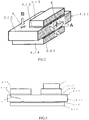
- the top view of this circuit board 1 and the cross sectional view in I-I direction are shown in figure 1 .
- metal circuit plate 3 and metal heat sink 4 are bonded to one face and to another face respectively, of insulating-ceramics substrate 2, via brazing material 5.
- insulating-ceramics substrate 2 silicon nitride ceramics are used, for example.
- brazing material 5 is composed of an active metal, typically Ag-Cu system alloy to which Ti is doped for example, and by using this, metal circuit plate 3 and heat sink 4 are bonded to insulating-ceramics substrate 2 at the temperature of about 750 °C.
- a semiconductor module using this circuit board 1 is formed by bonding and mounting a semiconductor chip (not shown) with solder on metal circuit plate 3.
- K H1 of this circuit board 1 is 3.0 - 6.5MPa ⁇ m 1/2 .
- K H1 is a value showing in-plane expansion of the crack of insulating-ceramics substrate 2, and this depends on both fracture toughness value of insulating-ceramics substrate 2 itself and residual stress in insulating-ceramics substrate 2.
- in-plane fracture toughness value K H of insulating-ceramics substrate 2 is defined as "in-plane fracture toughness value K H of insulating-ceramics substrate 2"
- in-plane apparent fracture toughness value K H1 of circuit board 1 is defined by the residual stress intensity factor depending on the fracture toughness value of insulating-ceramics substrate 2, and on the intensity of the residual stress in insulating-ceramics substrate 2.
- the mechanical property about expansion of the crack in insulating-ceramics substrate 2 to which metal circuit plate 3 and metal heat sink 4 are bonded in circuit board 1, can be understood using the apparent fracture toughness value.
- a crack generated in insulating-ceramics substrate 2 by the stress caused by the thermal expansion difference between insulating-ceramics substrate 2 and metal plates may easily expand in the in-plane direction of insulating-ceramics substrate 2.
- circuit board 1 with high reliability using insulating-ceramics substrate 2 in which in-plane apparent fracture toughness value K H1 is set at 3.0 MPa ⁇ m 1/2 or higher, and a crack is made hard to be generated and which is hard to be broken, can be given.
- in-plane apparent fracture toughness value K H1 is extremely high, when being higher than 6.5 MPa ⁇ m 1/2 , the anisotropy of the apparent fracture toughness value is high, therefore apparent fracture toughness value along the thickness direction becomes low, therefore, a crack may extend easily along the thickness direction. Therefore, in-plane apparent fracture toughness value K H1 is preferred to be 6.5 MPa ⁇ m 1/2 or lower.
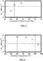
- the outline of the measuring method of K H1 and K H1 is shown in figure 2 .
- square shaped indentation 6 is formed, so that the directions of diagonal lines are parallel to the in-plane direction (horizontal direction), and thickness direction (vertical direction) respectively.
- the length of the diagonal lines of indentation 6 is set equal in both directions, and the lengths are set to be 2a.
- the crack in insulating-ceramics substrate 2 is generated along the direction of these diagonal lines, as shown in figure 2 , and the length is 2c 1 along the horizontal direction, and is 2c 2 along the vertical direction, respectively.
- FIG. 3 the schematic diagram of a crack generated during the thermal cycles is shown in figure 3 .
- semiconductor chip 7 is bonded and mounted on metal circuit plate 3.
- Crack 8 is generated near the surface of the peripheral part of the pattern of metal circuit plate 3 on insulating-ceramics substrate 2, and generally, this crack may extend horizontally inside insulating-ceramics substrate 2, as shown in figure 3 .
- especially compressive stress may be easily generated along the thickness direction.
- by making the in-plane apparent fracture toughness value at 3.0 MPa ⁇ m 1/2 or higher especially horizontal expansion of this crack is suppressed.
- the difference between the in-plane fracture toughness value K H of insulating-ceramics substrate 2 and the in-plane apparent fracture toughness value K H1 of circuit board 1, K H - K H1 is set at 3.0 MPa ⁇ m 1/2 or less.
- the difference between the in-plane apparent fracture toughness value of circuit board 1 and the in-plane fracture toughness value of insulating-ceramics substrate 2 depends on the intensity of the residual stress applied to insulating-ceramics substrate 2 in circuit board 1. Therefore, the residual stress applied to insulating-ceramics substrate 2 was made low by this composition.
- circuit board 1 becomes 3.0 - 6.5 MPa ⁇ m 1/2 , and a crack which extended into insulating-ceramics substrate 2 from the peripheral part of metal circuit plate 3 bonded to insulating-ceramics substrate 2, did not extend more widely, and the substrate was not broken.
- the amount of camber of circuit board 1 was made 80 ⁇ m / inch (1 inch is 0.0254m) or less, and the residual stress applied to insulating-ceramics substrate 2 was made low.
- the in-plane apparent fracture toughness value K H1 of circuit board 1 becomes 3.0 - 6.5 MPa ⁇ m 1/2 , and a crack which extended into insulating-ceramics substrate 2 from the peripheral part of metal circuit plate 3 bonded to insulating-ceramics substrate 2, did not extend more widely, and the substrate was not broken.
- the in-plane fracture toughness value of insulating-ceramics substrate 2 was set at 5.5 MPa • m 1/2 or higher, and also setting the thickness at 0.2mm or larger, the residual stress applied to insulating-ceramics substrate 2 was made low.
- this range may be preferred also.
- the in-plane apparent fracture toughness value K H1 of circuit board 1 becomes 3.0 - 6.5 MPa ⁇ m 1/2 , and a crack which extended into insulating-ceramics substrate 2 from the peripheral part of metal circuit plate 3 bonded to insulating-ceramics substrate 2, did not extend more widely, and the substrate was not broken.
- the fracture toughness value of silicon nitride ceramics used as insulating-ceramics substrate 2 depends on species of raw materials, composition and addition of sintering aids, or sintering conditions, etc. Therefore, pillar-shaped particles are grown, and number of grain boundaries and composition of that in ceramics are optimized, and strength of the grain boundaries can be made high, by optimizing these manufacturing conditions.
- thickness of insulating-ceramics substrate 2 may be set at 1.0 mm or less, preferably.
- a ratio (area ratio) of gross area of metal circuit plate 3 to gross area of metal heat sink 4 was set at 5/9 or more.
- structure of metal circuit plate 3 and metal heat sink 4 bonded to insulating-ceramics substrate 2 is preferred to be almost uniform.
- circuit patterns are formed in metal circuit plate 3 actually, non-circuit formation part where metal circuit plate 3 is not bonded and circuit formation part where metal circuit plate 3 is bonded, are existing on one face of insulating-ceramics substrate 2.
- metal circuit plate 3 and metal heat sink 4 it is preferred that it is a 0.5-5.0 mm-thick copper plate.
- copper plate with thickness of 0.5 mm or larger as metal circuit plate 3 and metal heat sink 4 circuit board 1 with high heat dissipation can be obtained, and by setting the thickness at 5.0mm or less, the residual stress caused by the thermal expansion difference of insulating-ceramics substrate 2, metal circuit plate 3, and metal heat sink 4 can be lowered, and circuit board 1 with in-plane apparent fracture toughness value K H1 of 3.0 - 6.5 MPa ⁇ m 1/2 and with high reliability can be obtained. And endurance against thermal cycles may be improved.
- bonding between insulating-ceramics substrate 2 and metal circuit plate 3, and bonding between insulating-ceramics substrate 2 and metal heat sink 4, were carried out via brazing material 5 which is an active metal, by heating at 600 - 900 °C.
- the residual stress applied to insulating-ceramics substrate 2 is caused by the thermal expansion difference between insulating-ceramics substrate 2 and metal plate of metal circuit plate 3 and of metal heat sink 4, during the bonding. Therefore, by making bonding temperature low at 900 °C or lower, thermal expansion difference of insulating-ceramics substrate 2 and the metal plates can be lowered, and the residual stress can be lowered.
- the reliability of the bonding may become insufficient when bonding at the low temperature below 600 °C. Then, by bonding the metal plates on insulating-ceramics substrate 2 via active metal brazing material, and setting the bonding temperature at 600 °C - 900 °C, residual stress caused by the thermal expansion difference of insulating-ceramics substrate 2, metal circuit plate 3, and metal heat sink 4, can be lowered, and circuit board 1 with in-plane apparent fracture toughness value K H1 of 3.0 - 6.5 MPa ⁇ m 1/2 and with high reliability can be obtained.
- Metal brazing material such as Ag-Cu system alloy paste with Ti doped, which is an active metal, is printed on both faces of insulating-ceramics substrate 2 (silicon nitride ceramics), and metal (copper) plates with almost same rectangular shape as insulating-ceramics substrate 2 are heated and bonded at temperature of 600 °C - 900 °C to both faces.
- metal circuit plate 3 is formed by carrying out etching process on the metal plate on one face so that it forms circuit pattern.
- Another metal plate bonded to another face may be used as metal heat sink 4 without etching process, or may be used as metal heat sink 4 as patterned similarly.
- Ni-P plating is carried on metal circuit plate 3 and metal heat sink 4 after the circuit pattern formation, and circuit board 1 is produced.
- a semiconductor module is formed, by mounting a semiconductor chip on above-mentioned circuit board 1.
- metal circuit plate 3 and the semiconductor chip are bonded via solder.
- This semiconductor module has high endurance against thermal cycles.
- Circuit board 11 concerning a 2nd embodiment of this invention can be applied irrespective of degree of the anisotropy of insulating-ceramics substrate.
- the structure of this circuit board 11 is similar to that of circuit board 1 concerning a 1st aforementioned embodiment, and that top view and the sectional view in I-I direction are shown in figure 1 .
- metal circuit plate 13 and metal heat sink 14 are bonded to one face and to another face respectively, of insulating-ceramics substrate 12, via metal brazing material 15.
- thickness of insulating-ceramics substrate 12 is shown as "t c "
- thickness of metal circuit plate 13 is shown as "t 1 "
- thickness of metal heat sink 14 is shown as "t 2 ".
- the thickness of brazing material 15 is negligibly small to them.
- As insulating-ceramics substrate 12 silicon nitride ceramics is used, for example.
- Brazing material 15 is an active metal such as Ag-Cu system alloy in which Ti is doped, for example, by using this, metal circuit plate 13 and metal heat sink 4 are bonded to insulating-ceramics substrate 12 at temperature of around 750 °C.
- internal apparent fracture toughness value K 1 of circuit board 11 is 4.0 MPa ⁇ m 1/2 or higher.
- internal apparent fracture toughness value of circuit board 11 is measured in circuit board 11 with structure in which metal circuit plate 13 is bonded on one face of insulating-ceramics substrate 12 and metal heat sink 14 is bonded on another face of that, by IF method, in which Vickers indenter is pushed to cross section of insulating-ceramics substrate 12 along "A" direction in figure.2 with a predetermined load (for example 2kgf) as described in JISR1607 (Japan).
- internal fracture toughness value K is a fracture toughness value similarly measured in insulating-ceramics substrate 12 before metal circuit plate 13 and metal heat sink 14 are bonded.
- K 1 depends on the fracture toughness value of insulating-ceramics substrate 12 itself and on residual stress applied to insulating-ceramics substrate 12. For example, when tensile residual stress is working, a crack may expand easily especially along a perpendicular direction to the tensile stress, therefore, internal apparent fracture toughness value K 1 becomes low in this case.
- internal apparent fracture toughness value K 1 is computed like aforementioned in-plane apparent fracture toughness value K H1 by the method shown in figure 2 , after metal circuit plate 13 and metal heat sink 14 are bonded to insulating-ceramics substrate 12.
- fracture toughness values computed from horizontal crack and vertical crack are internal apparent fracture toughness value K 1 and internal fracture toughness value K, respectively. These are amounts which show the degree of anti-cracking along horizontal and vertical direction in insulating-ceramics substrate 12.
- Inside apparent fracture toughness value K 1 depends on internal fracture toughness value K of insulating-ceramics substrate 12, and also on thickness of the substrate "t c ", thickness of metal circuit plate 13 "t 1 ", and thickness of metal heat sink 14 "t 2 ".
- in-plane fracture toughness value of insulating-ceramics substrate 12 also varies by bonding metal circuit plate 13 and metal heat sink 14.
- the in-plane fracture toughness value was calculated by a method in which Vickers indenter was pushed along "B" direction in figure 2 , to a face of insulating-ceramics substrate 12, and was calculated by the indent and crack, similarly to the method for aforementioned internal fracture toughness value.
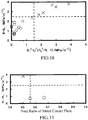
- the experimental results on relation between this life and in-plane apparent fracture toughness value is shown in figure 8 . Weaker correlation than figure 7 is found. Thereby, internal apparent fracture toughness value K1 is more effective on the life, than in-plane fracture toughness value. This fact shows that, when insulating-ceramics substrate 12 is broken during thermal cycles, internal expansion of the crack is more effective than in-plane expansion of the crack.
- internal apparent fracture toughness value K 1 becomes lower than internal fracture toughness value "K" of insulating-ceramics substrate 12, by bonding metal circuit plate 13 and metal heat sink 14. Because, tensile residual stress is generated inside insulating-ceramics substrate 12 after metal circuit plate 13 and metal heat sink 14 are bonded. Therefore, in order to make this effect weak and to keep internal apparent fracture toughness value K 1 high, thickness of metal circuit plate 13 and metal heat sink 14, "t 1 ", "t 2 " should be both small, and should be close to each other. Also, thickness of insulating-ceramics substrate 12 "t c " should be large, and internal fracture toughness value "K” should be large.
- index "x" is the thickness of insulating-ceramics substrate 12
- t 1 is the thickness of metal circuit plate 13
- t 2 is the thickness of metal heat sink 14
- K is the internal fracture toughness value of insulating-ceramics substrate 12, to express the aforementioned effect.
- x ⁇ 1.5 (1/MPa ⁇ m 1/2 )
- internal apparent fracture toughness value K 1 of insulating-ceramics substrate 12 became 4.0 MPa • m 1/2 or higher, therefore, long life against thermal cycles was obtained in the semiconductor module using this circuit board 11.
- K 1 is always smaller than K (K - K 1 > 0), and it is found that, when setting x ⁇ 1.5 (1/MPa/m 1/2 ), K-K 1 becomes 2.5 MPa ⁇ m 1/2 or lower, and long life against thermal cycles is obtained.
- the ratio (area ratio) of the gross area of metal circuit plate 13 to the gross area of metal heat sink 14 was set at 5/9 (0.556) or larger.
- this ratio is smaller than 5/9, since the residual stress applied to insulating-ceramics substrate 12 will become high, long life cannot be obtained.
- the maximum of this area ratio is 1 obviously by that definition.
- Many circuit boards 11 with various gross area of metal circuit plates 13 were fabricated, and experimental results on relation between the area ratio and aforementioned K - K 1 are shown in figure 11 . From these results, it is found that, as the area ratio is small, K - K 1 becomes large, and by setting the area ratio at 5/9 or larger, long life against thermal cycles can be obtained.
- Thickness of metal circuit plate 13 and metal heat sink 14 were in the range of 0.5 - 5.0mm. Thermal dissipation is not enough when the thickness is smaller than 0.5mm, and the volume of the semiconductor module becomes large and becomes heavy and not practical when the thickness is larger than 5.0mm.
- thickness of metal circuit plate 13 and metal heat sink 14 shall be 0.8 - 5.0mm, and in this case, since the camber of circuit board 11 caused by thermal expansion difference becomes still larger, the effect by setting "x" into the above-mentioned range is remarkable.
- Thickness of insulating-ceramics substrate 12 is preferred to be large as aforementioned, although is preferred to be around 0.2 - 1. 0mm concretely. When being thinner than 0.2mm, it may be broken easily by thermal stress when metal circuit plate 13 and metal heat sink 14 are bonded, even if the fracture toughness is high, and when being thicker than 1.0mm, the thermal resistance and inductance of the semiconductor module become high, and is not preferred.
- about the lower limit at 0.2mm even if the thickness is set at 0.2mm ⁇ 0.02mm, no generation of a crack was found, therefore, this range may be preferred also.
- internal fracture toughness values "K" is preferred to be 5.5 - 7.5 MPa ⁇ m 1/2 .
- silicon nitride ceramics are preferably used as an insulating-ceramics substrate with such characteristics.
- brazing material 5 is composed of an active metal, typically Ag-Cu system alloy to which Ti is doped for example.
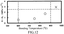
- bonding temperature is preferred to be 600 - 900 °C.
- bonding strength will become poor, and when being higher than 900 °C, residual stress applied to insulating-ceramics substrate 12 becomes high, because thermal expansion difference between insulating-ceramics substrate 12 and metal circuit plate 13 becomes large.
- Experimental results on relation between the bonding temperature and aforementioned K - K 1 are shown in figure 12 , similarly to figure 11 . From these results, as this temperature is high, K - K 1 becomes large, and it is found that endurance against thermal cycles is improved by setting the temperature at 900 °C or lower.
- the above-mentioned circuit board 11 can be produced by the similar production method as the aforementioned circuit board 1. Also a semiconductor module using this can be fabricated similarly. This semiconductor module has high endurance against thermal cycles.
- metal circuit plates and metal heat sinks were bonded to insulating-ceramics substrate by brazing material although when other methods are used, high endurance can be obtained similarly.
- In-plane fracture toughness values K, internal fracture toughness values K H , and thickness of silicon nitride ceramics substrates, and thickness of metal circuit plates and metal heat sinks, are shown in Table 1.
- Active metal brazing materials were printed on both faces of silicon nitride ceramics substrates, and copper plates with almost same rectangular shape as the silicon nitride substrates were heated and bonded to the both faces of silicon nitride ceramics substrates at temperature of 600 - 900 °C. Each temperature (bonding temperature) is shown in Table 1. After cooling, these were etched so that metal circuit plates and metal heat sinks might form predetermined patterns, and Ni - P plating was carried on the metal circuit plate and the metal heat sink, and the circuit boards was produced.
- thermal cycle tests were done.
- One cycle in the thermal cycle test comprised heating and cooling steps, in which cooling for 20 minutes at -55 °C, keeping for 10 minutes at room temperature, and heating for 20 minutes at 150 °C were done.
- generation of a crack of silicon nitride ceramics substrates and of a delamination of metal circuit plates was evaluated. Generation of a crack was investigated by fluorescent crack probing method. It is shown that whether generation of a crack was found or not after the thermal cycle test, in Table 1.
- thickness of silicon nitride ceramics substrates t c (mm), internal fracture toughness value K (MPa ⁇ m 1/2 ), thickness of metal circuit plates t 1 (mm), and thickness of the heat sinks t 2 (mm), were varied so that (t 1 2 -t 2 2 ) /t c 2 /K ⁇ 1.5.
- the thickness of metal circuit plates and that of metal heat sinks were set in the range of 0.5 - 5.0mm. Area ratio of the gross area of metal circuit plate to the gross area of the metal heat sink was 5/9 or larger. Bonding temperature was lower than 900 °C, and was 600 °C or higher. By these conditions, the in-plane fracture toughness values were set in the range of 3.0 - 6.5 MPa ⁇ m 1/2
Claims (8)
- Carte de circuit imprimé comprenant un substrat en céramique isolante (2, 12) composé de céramique nitrure de silicium, une plaque métallique de circuit imprimé (3) et un dissipateur thermique métallique (4), possédant une structure dans laquelle une face de ladite plaque métallique de circuit imprimé est liée à une face dudit substrat en céramique isolante, une face dudit dissipateur thermique métallique est liée à une autre face dudit substrat en céramique isolante, et le substrat en céramique n'est lié ni à une autre face de ladite plaque métallique de circuit imprimé ni à une autre face dudit dissipateur thermique métallique, caractérisée en ce que :une valeur de ténacité à la rupture dans le plan dudit substrat en céramique isolante, estimée à partir d'une longueur de fissure horizontale formée par un pénétrateur Vickers sur une section verticale dudit substrat en céramique isolante seul, est supérieure ou égale à 5,5 MPa ·m1/2,une épaisseur dudit substrat en céramique isolante se situe dans la plage de 0,2 à 1,0 mm,ladite plaque métallique de circuit imprimé et ledit dissipateur thermique métallique sont tous deux constitués de cuivre, et l'épaisseur de ladite plaque métallique de circuit imprimé ainsi que l'épaisseur dudit dissipateur thermique métallique sont égales et se situent dans la plage de 0,5 à 5 mm,un rapport de l'aire totale de ladite plaque métallique de circuit imprimé à l'aire totale dudit dissipateur thermique métallique est supérieur ou égal à 5/9,ladite plaque métallique de circuit imprimé est liée audit substrat en céramique isolante et ledit dissipateur thermique métallique est lié audit substrat en céramique isolante par le biais d'un métal d'apport de brasage actif,et une température de liaison est réglée à une valeur de 600 °C à 850 °C,une valeur de ténacité à la rupture interne dudit substrat en céramique isolante, estimée à partir de longueurs de fissures à la fois horizontales et verticales formées par un pénétrateur Vickers sur une section verticale dudit substrat en céramique isolante seul, se situe dans la plage de 5,5 ∼ 7,5 MPa ·m1/2,une valeur de ténacité à la rupture apparente dans le plan de ladite carte de circuit imprimé, estimée à partir d'une longueur de fissure horizontale formée par un pénétrateur Vickers sur une section verticale dudit substrat en céramique isolante auquel ladite plaque métallique de circuit imprimé et ledit dissipateur thermique métallique sont tous deux liés se situe dans la plage de 3,0 à 6,5 MPa ·m1/2,une valeur absolue de grandeur de cambrure de ladite carte de circuit imprimé est inférieure ou égale à 80 pm/pouce (2,54 cm).
- Carte de circuit imprimé selon la revendication 1,
dans laquelle une différence entre ladite valeur de ténacité à la rupture dans le plan de ladite céramique isolante et ladite valeur de ténacité à la rupture apparente dans le plan de ladite carte de circuit imprimé est inférieure ou égale à 3,0 MPa ·m1/2. - Carte de circuit imprimé selon la revendication 1 ou 2,
dans laquelle ladite plaque métallique de circuit imprimé et ledit dissipateur thermique métallique présentent chacun une épaisseur de 0,8 ∼ 5,0 mm. - Carte de circuit imprimé selon l'une des revendications 1 à 3,
dans laquelle une valeur de ténacité à la rupture apparente interne de ladite carte de circuit imprimé, estimée à partir de longueurs de fissures à la fois horizontales et verticales formées par un pénétrateur Vickers sur une section verticale dudit substrat en céramique isolante auquel ladite plaque métallique de circuit imprimé et ledit dissipateur thermique métallique sont tous deux liés est supérieure ou égale à 4,0 MPa ·m1/2. - Carte de circuit imprimé selon l'une des revendications 1 à 4,
dans laquelle une différence entre ladite valeur de ténacité à la rupture interne dudit substrat en céramique isolante et ladite valeur de ténacité à la rupture apparente interne de ladite carte de circuit imprimé est inférieure ou égale à 2,5 MPa ·m1/2. - Procédé de production d'une carte de circuit imprimé pour produire une carte de circuit imprimé selon la revendication 1, le procédé comprenant un substrat en céramique isolante composé de céramique nitrure de silicium, une plaque métallique de circuit imprimé et un dissipateur thermique métallique,
possédant une structure dans laquelle une face de ladite plaque métallique de circuit imprimé est liée à une face dudit substrat en céramique isolante, une face dudit dissipateur thermique métallique est liée à une autre face dudit substrat en céramique isolante, et le substrat en céramique n'est lié ni à une autre face de ladite plaque métallique de circuit imprimé ni à une autre face dudit dissipateur thermique métallique,
une valeur de ténacité à la rupture dans le plan dudit substrat en céramique isolante, estimée à partir d'une longueur de fissure horizontale formée par un pénétrateur Vickers sur une section verticale dudit substrat en céramique isolante seul, est supérieure ou égale à 5,5 MPa ·m1/2,
une épaisseur dudit substrat en céramique isolante se situe dans la plage de 0,2 à 1,0 mm,
ladite plaque métallique de circuit imprimé et ledit dissipateur thermique métallique sont tous deux constitués de cuivre, et l'épaisseur de ladite plaque métallique de circuit imprimé ainsi que l'épaisseur dudit dissipateur thermique métallique sont égales et se situent dans la plage de 0,5 à 5 mm,
un rapport de l'aire totale de ladite plaque métallique de circuit imprimé à l'aire totale dudit dissipateur thermique métallique est supérieur ou égal à 5/9,
une valeur de ténacité à la rupture interne dudit substrat en céramique isolante, estimée à partir de longueurs de fissures à la fois horizontales et verticales formées par un pénétrateur Vickers sur une section verticale dudit substrat en céramique isolante seul, se situe dans la plage de 5,5 ∼ 7,5 MPa ·m1/2,
ladite plaque métallique de circuit imprimé est liée audit substrat en céramique isolante et ledit dissipateur thermique métallique est lié audit substrat en céramique isolante par le biais d'un métal d'apport de brasage actif, et une température de liaison est réglée à une valeur de 600 °C à 850 °C. - Procédé de production de la carte de circuit imprimé, selon la revendication 6,
dans lequel ladite plaque métallique de circuit imprimé et ledit dissipateur thermique métallique présentent chacun une épaisseur de 0,8 ∼ 5,0 mm. - Module à semi-conducteur comprenant la carte de circuit imprimé selon l'une des revendications 1 à 5, et une puce à semi-conducteur montée sur ladite carte de circuit imprimé.
Applications Claiming Priority (3)
| Application Number | Priority Date | Filing Date | Title |
|---|---|---|---|
| JP2005247301 | 2005-08-29 | ||
| JP2006091408 | 2006-03-29 | ||
| PCT/JP2006/316154 WO2007026547A1 (fr) | 2005-08-29 | 2006-08-17 | Carte à circuit imprimé et module à semiconducteur utilisant celle-ci, procédé de fabrication pour carte à circuit imprimé |
Publications (3)
| Publication Number | Publication Date |
|---|---|
| EP1921675A1 EP1921675A1 (fr) | 2008-05-14 |
| EP1921675A4 EP1921675A4 (fr) | 2010-09-22 |
| EP1921675B1 true EP1921675B1 (fr) | 2018-10-31 |
Family
ID=37808647
Family Applications (1)
| Application Number | Title | Priority Date | Filing Date |
|---|---|---|---|
| EP06782767.5A Active EP1921675B1 (fr) | 2005-08-29 | 2006-08-17 | Carte a circuit imprime et module a semiconducteur utilisant celle-ci, procede de fabrication pour carte a circuit imprime |
Country Status (4)
| Country | Link |
|---|---|
| US (1) | US8563869B2 (fr) |
| EP (1) | EP1921675B1 (fr) |
| JP (3) | JP5326278B2 (fr) |
| WO (1) | WO2007026547A1 (fr) |
Families Citing this family (27)
| Publication number | Priority date | Publication date | Assignee | Title |
|---|---|---|---|---|
| WO2007026547A1 (fr) * | 2005-08-29 | 2007-03-08 | Hitachi Metals, Ltd. | Carte à circuit imprimé et module à semiconducteur utilisant celle-ci, procédé de fabrication pour carte à circuit imprimé |
| JP2009094264A (ja) * | 2007-10-09 | 2009-04-30 | Hitachi Metals Ltd | 回路基板、半導体モジュール、半導体モジュールの設計方法 |
| JP2009130060A (ja) * | 2007-11-21 | 2009-06-11 | Toyota Industries Corp | 放熱装置 |
| JP5070014B2 (ja) * | 2007-11-21 | 2012-11-07 | 株式会社豊田自動織機 | 放熱装置 |
| KR20110015544A (ko) * | 2008-05-16 | 2011-02-16 | 미쓰비시 마테리알 가부시키가이샤 | 파워 모듈용 기판, 파워 모듈, 및 파워 모듈용 기판의 제조 방법 |
| JPWO2009154295A1 (ja) * | 2008-06-20 | 2011-12-01 | 日立金属株式会社 | セラミックス集合基板とその製造方法及びセラミックス基板並びにセラミックス回路基板 |
| DE102010039728A1 (de) * | 2010-08-25 | 2012-03-01 | Robert Bosch Gmbh | Verfahren zur Herstellung einer elektrischen Schaltung und elektrischen Schaltung |
| EP2811513B1 (fr) | 2012-02-01 | 2019-12-18 | Mitsubishi Materials Corporation | Procédé de fabrication de substrat pour modules de courant |
| CN102856266A (zh) * | 2012-09-19 | 2013-01-02 | 张剑锋 | 一体化绝缘陶瓷基板 |
| EP3109222B1 (fr) * | 2014-02-21 | 2018-09-26 | Denka Company Limited | Substrat de circuit en céramique |
| JP6341822B2 (ja) * | 2014-09-26 | 2018-06-13 | 三菱電機株式会社 | 半導体装置 |
| CN105742268B (zh) * | 2014-12-26 | 2019-01-22 | 株式会社东芝 | 布线基板以及包含布线基板的半导体封装 |
| CN107112299B (zh) * | 2015-01-29 | 2019-10-01 | 京瓷株式会社 | 电路基板以及电子装置 |
| JP6370257B2 (ja) | 2015-04-27 | 2018-08-08 | 三菱電機株式会社 | 半導体装置 |
| KR101708317B1 (ko) * | 2015-06-17 | 2017-02-20 | 엘지전자 주식회사 | 스트레인 검사 소자 및 그 부착 방법 |
| WO2017056360A1 (fr) * | 2015-09-28 | 2017-04-06 | 株式会社 東芝 | Substrat de circuit et dispositif à semi-conducteur |
| JP6829204B2 (ja) * | 2015-09-28 | 2021-02-10 | 株式会社東芝 | 窒化珪素回路基板およびそれを用いた半導体モジュール |
| JP6137267B2 (ja) * | 2015-10-08 | 2017-05-31 | 三菱マテリアル株式会社 | ヒートシンク付きパワーモジュール用基板及びパワーモジュール |
| CN110226363B (zh) * | 2017-03-30 | 2022-08-02 | 株式会社东芝 | 陶瓷铜电路基板及使用了其的半导体装置 |
| JP7127641B2 (ja) * | 2017-05-11 | 2022-08-30 | 住友電気工業株式会社 | 半導体装置 |
| KR102436225B1 (ko) * | 2017-07-28 | 2022-08-25 | 삼성전기주식회사 | 인쇄회로기판 |
| JPWO2019167942A1 (ja) * | 2018-02-27 | 2020-04-16 | 三菱マテリアル株式会社 | 絶縁回路基板 |
| DE102018104521B4 (de) | 2018-02-28 | 2022-11-17 | Rogers Germany Gmbh | Metall-Keramik-Substrate |
| EP3951854A4 (fr) * | 2019-03-29 | 2022-05-25 | Denka Company Limited | Carte de circuit imprimé de nitrure de silicium et module de composant électronique |
| CN110012597B (zh) * | 2019-04-12 | 2020-11-27 | 中国科学院电工研究所 | 一种陶瓷覆铜电路板及其制备方法 |
| CN114303237A (zh) * | 2019-08-29 | 2022-04-08 | 京瓷株式会社 | 电路基板及功率模块 |
| WO2023204054A1 (fr) * | 2022-04-18 | 2023-10-26 | 株式会社 東芝 | Substrat de circuit en céramique, dispositif à semi-conducteur, procédé de fabrication de substrat de circuit en céramique et procédé de fabrication de dispositif à semi-conducteur |
Family Cites Families (15)
| Publication number | Priority date | Publication date | Assignee | Title |
|---|---|---|---|---|
| US5780164A (en) | 1994-12-12 | 1998-07-14 | The Dow Chemical Company | Computer disk substrate, the process for making same, and the material made therefrom |
| US5672435A (en) * | 1994-12-12 | 1997-09-30 | The Dow Chemical Company | Hard disk drive components and methods of making same |
| JP3100871B2 (ja) | 1995-07-11 | 2000-10-23 | 株式会社東芝 | 窒化アルミニウム焼結体 |
| JP3932343B2 (ja) | 1996-08-27 | 2007-06-20 | Dowaメタルテック株式会社 | 半導体用基板およびその製造方法 |
| JP3512977B2 (ja) | 1996-08-27 | 2004-03-31 | 同和鉱業株式会社 | 高信頼性半導体用基板 |
| JPH10107440A (ja) * | 1996-09-30 | 1998-04-24 | Sumitomo Kinzoku Electro Device:Kk | セラミック基板及びその製造方法 |
| JP2001010865A (ja) | 1999-06-23 | 2001-01-16 | Ngk Insulators Ltd | 窒化珪素焼結体及びその製造方法 |
| US6417563B1 (en) * | 2000-07-14 | 2002-07-09 | Advanced Micro Devices, Inc. | Spring frame for protecting packaged electronic devices |
| DE10146227B4 (de) * | 2000-09-20 | 2015-01-29 | Hitachi Metals, Ltd. | Siliciumnitrid-Sinterkörper, Leiterplatte und thermoelektrisches Modul |
| JP3797905B2 (ja) | 2000-10-27 | 2006-07-19 | 株式会社東芝 | 窒化けい素セラミックス基板およびそれを用いた窒化けい素セラミックス回路基板並びにその製造方法 |
| EP1201623B1 (fr) | 2000-10-27 | 2016-08-31 | Kabushiki Kaisha Toshiba | Substrat en nitrure de silicium et plaquette de circuit ceramique utilisant le substrat |
| JP2003101184A (ja) * | 2001-09-27 | 2003-04-04 | Kyocera Corp | セラミック回路基板およびその製造方法 |
| JP2004119568A (ja) * | 2002-09-25 | 2004-04-15 | Kyocera Corp | セラミック回路基板 |
| JP4360847B2 (ja) * | 2003-06-30 | 2009-11-11 | 日本特殊陶業株式会社 | セラミック回路基板、放熱モジュール、および半導体装置 |
| WO2007026547A1 (fr) * | 2005-08-29 | 2007-03-08 | Hitachi Metals, Ltd. | Carte à circuit imprimé et module à semiconducteur utilisant celle-ci, procédé de fabrication pour carte à circuit imprimé |
-
2006
- 2006-08-17 WO PCT/JP2006/316154 patent/WO2007026547A1/fr active Application Filing
- 2006-08-17 JP JP2007533174A patent/JP5326278B2/ja active Active
- 2006-08-17 EP EP06782767.5A patent/EP1921675B1/fr active Active
- 2006-08-17 US US12/065,009 patent/US8563869B2/en active Active
-
2012
- 2012-06-11 JP JP2012131557A patent/JP2012169678A/ja active Pending
- 2012-10-19 JP JP2012231919A patent/JP5598522B2/ja active Active
Non-Patent Citations (1)
| Title |
|---|
| None * |
Also Published As
| Publication number | Publication date |
|---|---|
| WO2007026547A1 (fr) | 2007-03-08 |
| JP2012169678A (ja) | 2012-09-06 |
| JP5326278B2 (ja) | 2013-10-30 |
| US8563869B2 (en) | 2013-10-22 |
| JP5598522B2 (ja) | 2014-10-01 |
| JP2013042165A (ja) | 2013-02-28 |
| EP1921675A1 (fr) | 2008-05-14 |
| EP1921675A4 (fr) | 2010-09-22 |
| US20090101392A1 (en) | 2009-04-23 |
| JPWO2007026547A1 (ja) | 2009-03-05 |
Similar Documents
| Publication | Publication Date | Title |
|---|---|---|
| EP1921675B1 (fr) | Carte a circuit imprime et module a semiconducteur utilisant celle-ci, procede de fabrication pour carte a circuit imprime | |
| JP4969738B2 (ja) | セラミックス回路基板およびそれを用いた半導体モジュール | |
| EP2214201B1 (fr) | Procédé de fabrication de substrat pour module de puissance, substrat pour module de puissance, et module de puissance | |
| CN101971329B (zh) | 带散热片的功率模块用基板及其制造方法、以及带散热片的功率模块、功率模块用基板 | |
| CN104718615B (zh) | 半导体电路板及其制造方法和使用其的半导体装置 | |
| KR101975633B1 (ko) | 금속-세라믹스 접합 기판 및 그 제조 방법 | |
| CN110383468A (zh) | 带散热片的功率模块用基板 | |
| JP2017191943A (ja) | セラミックス回路基板の製造方法 | |
| JP4893096B2 (ja) | 回路基板およびこれを用いた半導体モジュール | |
| WO2011149065A1 (fr) | Carte de circuit imprimé et dispositif électronique doté d'une telle carte | |
| JP2003163315A (ja) | モジュール | |
| CN106537580B (zh) | 陶瓷电路基板及其制造方法 | |
| JP2007142126A (ja) | 複合材料及び半導体搭載用放熱基板、及びそれを用いたセラミックパッケージ | |
| JP2007299973A (ja) | 回路基板およびこれを用いた半導体モジュール | |
| JP5218621B2 (ja) | 回路基板およびこれを用いた半導体モジュール | |
| EP3605601A1 (fr) | Procédé de production d'une carte de circuit imprimé isolée pourvue d'un dissipateur thermique | |
| JP5370460B2 (ja) | 半導体モジュール | |
| EP3761764A1 (fr) | Carte de circuit imprimé isolante | |
| JP3932744B2 (ja) | 半導体実装用絶縁回路基板の製造方法 | |
| JP2009158576A (ja) | 電子部品検査治具用多層セラミック基板 | |
| JP4124040B2 (ja) | 半導体装置 | |
| JP2006229247A (ja) | 回路基板及びその製造方法 | |
| EP3761351B1 (fr) | Carte de circuit isolée | |
| JPH0477369A (ja) | 金属・セラミックス複合基板の製造方法 | |
| JP4515562B2 (ja) | セラミックス回路基板の製造方法 |
Legal Events
| Date | Code | Title | Description |
|---|---|---|---|
| PUAI | Public reference made under article 153(3) epc to a published international application that has entered the european phase |
Free format text: ORIGINAL CODE: 0009012 |
|
| 17P | Request for examination filed |
Effective date: 20080222 |
|
| AK | Designated contracting states |
Kind code of ref document: A1 Designated state(s): DE FR |
|
| RBV | Designated contracting states (corrected) |
Designated state(s): DE FR |
|
| A4 | Supplementary search report drawn up and despatched |
Effective date: 20100823 |
|
| RIC1 | Information provided on ipc code assigned before grant |
Ipc: H01L 23/15 20060101AFI20070516BHEP Ipc: H01L 23/373 20060101ALI20100813BHEP |
|
| DAX | Request for extension of the european patent (deleted) | ||
| 17Q | First examination report despatched |
Effective date: 20130225 |
|
| GRAP | Despatch of communication of intention to grant a patent |
Free format text: ORIGINAL CODE: EPIDOSNIGR1 |
|
| INTG | Intention to grant announced |
Effective date: 20180524 |
|
| GRAS | Grant fee paid |
Free format text: ORIGINAL CODE: EPIDOSNIGR3 |
|
| GRAA | (expected) grant |
Free format text: ORIGINAL CODE: 0009210 |
|
| AK | Designated contracting states |
Kind code of ref document: B1 Designated state(s): DE FR |
|
| REG | Reference to a national code |
Ref country code: DE Ref legal event code: R096 Ref document number: 602006056728 Country of ref document: DE |
|
| REG | Reference to a national code |
Ref country code: DE Ref legal event code: R097 Ref document number: 602006056728 Country of ref document: DE |
|
| PLBE | No opposition filed within time limit |
Free format text: ORIGINAL CODE: 0009261 |
|
| STAA | Information on the status of an ep patent application or granted ep patent |
Free format text: STATUS: NO OPPOSITION FILED WITHIN TIME LIMIT |
|
| 26N | No opposition filed |
Effective date: 20190801 |
|
| PG25 | Lapsed in a contracting state [announced via postgrant information from national office to epo] |
Ref country code: FR Free format text: LAPSE BECAUSE OF NON-PAYMENT OF DUE FEES Effective date: 20190831 |
|
| REG | Reference to a national code |
Ref country code: DE Ref legal event code: R082 Ref document number: 602006056728 Country of ref document: DE Representative=s name: GRUENECKER PATENT- UND RECHTSANWAELTE PARTG MB, DE |
|
| REG | Reference to a national code |
Ref country code: DE Ref legal event code: R081 Ref document number: 602006056728 Country of ref document: DE Owner name: PROTERIAL, LTD., JP Free format text: FORMER OWNER: HITACHI METALS, LTD., TOKYO, JP |
|
| PGFP | Annual fee paid to national office [announced via postgrant information from national office to epo] |
Ref country code: DE Payment date: 20230627 Year of fee payment: 18 |