EP1916735B1 - Bias-Schaltung - Google Patents
Bias-Schaltung Download PDFInfo
- Publication number
- EP1916735B1 EP1916735B1 EP07020867.3A EP07020867A EP1916735B1 EP 1916735 B1 EP1916735 B1 EP 1916735B1 EP 07020867 A EP07020867 A EP 07020867A EP 1916735 B1 EP1916735 B1 EP 1916735B1
- Authority
- EP
- European Patent Office
- Prior art keywords
- reactance
- reactance means
- bias circuit
- frequency
- switch
- Prior art date
- Legal status (The legal status is an assumption and is not a legal conclusion. Google has not performed a legal analysis and makes no representation as to the accuracy of the status listed.)
- Ceased
Links
Images






Classifications
-
- H—ELECTRICITY
- H03—ELECTRONIC CIRCUITRY
- H03F—AMPLIFIERS
- H03F1/00—Details of amplifiers with only discharge tubes, only semiconductor devices or only unspecified devices as amplifying elements
- H03F1/30—Modifications of amplifiers to reduce influence of variations of temperature or supply voltage or other physical parameters
-
- H—ELECTRICITY
- H03—ELECTRONIC CIRCUITRY
- H03F—AMPLIFIERS
- H03F3/00—Amplifiers with only discharge tubes or only semiconductor devices as amplifying elements
- H03F3/189—High-frequency amplifiers, e.g. radio frequency amplifiers
Definitions
- the present invention relates to a bias circuit used for an amplifier and so on.
- a bias circuit in an amplifier application is connected to an AC circuit including an amplifying element, which is an active element, and supplies a DC voltage to the amplifying element without affecting transmission of a signal at a frequency to be amplified.
- Fig. 16 shows an example of a conventional bias circuit for an amplifier used in a device such as a radio device.
- the bias circuit 100p shown in Fig. 16 supplies a DC voltage to a field-effect transistor 180, which is an example of the active element that performs amplification.
- the bias circuit 100p includes a transmission line 181 one end of which is connected to the gate terminal 185 of a field-effect transistor 180 to which a DC voltage is applied, a capacitor 182 one end of which is connected to the other end of the transmission line 181 and the other end is grounded, a choke coil 183, which is a DC circuit, one end of which is connected to a connection point 186 between the transmission line 181 and the capacitor 182, and a DC power supply 184 which is connected to the other end of the choke coil 183 and generates a constant DC voltage with respect to a ground potential.
- the line length of the transmission line 181 is one-quarter of the wavelength of an operating frequency.
- the field-effect transistor is referred to as the FFT and the wavelength of a frequency is denoted by X.
- the capacitance of the capacitor 182 is chosen such that the impedance of the capacitor 182 becomes negligibly small at the frequency of an AC signal with a wavelength ⁇ .
- the transmission line 181 corresponds to an end short-circuited transmission line for the AC signal with the wavelength ⁇ . Because the transmission line 181 is 1/4-wavelength long as stated above, the impedance of the bias circuit 100p viewed from the gate terminal 185 of the FET 180 in the bias circuit 100p shown in Fig. 16 can be considered to be infinite at the AC signal frequency with wavelength X.
- the DC power supply 184 is connected in terms of direct current to the gate terminal 185 of the FET 180 through the choke coil 183 and the transmission line 181.
- a radio circuit such as an amplifier must be designed to operate at each of multiple frequency bands.
- One of the demands associated with designing radio circuits such as amplifiers for multiple frequency bands is to enable a bias circuit to operate at each of multiple frequency bands.
- Patent Literature 2 discloses a technology of using multiple conventional bias circuits to enable an amplifier to operate at each of multiple frequency bands.
- Patent Literature 3 Another technology is disclosed in Japanese Patent Laid-Open Application No. 2001-267864 (referred to as Patent Literature 3, hereinafter).
- the technology employs a configuration where the bias voltage of an active element adapts to working frequency bands, and thereby enables an amplifier to operate at each of multiple frequency bands by changing matching condition on the basis of significantly changing the input and output impedances of the amplifier.
- bias circuit arrangement is disclosed in EP 179 3634 .
- the disclosed bias circuit is capable of handling multiple frequency bands using switchable reactances.
- a bias circuit connected to an alternating-current circuit and being adapted to be operated at each of at least two operating frequencies according to claim 1.
- Fig. 1 shows a bias circuit according to a first embodiment of the present invention.
- the first embodiment is an example of the bias circuit which is used on the input terminal side of an amplifier.
- the bias circuit used for a dual-band amplifier circuit R1 is illustrated for facilitating understanding of the bias circuit according to the present invention.
- the amplification device may be such as a transistor, FET, MOSFET (Metal Oxide Semiconductor FET), or TFT (Thin Film Transistor). While an n-channel junction FET 180 is shown as the amplification device in each figure, it is not intended to limit the amplification device to an n-channel junction FET 180 but is only illustrative of the amplification device.
- An input circuit 300 of the amplifier circuit R1 shown in Fig. 1 includes a first input matching circuit 310, a second input matching circuit 320, and the bias circuit 100.
- An AC circuit 120 includes the first input matching circuit 310, the second input matching circuit 320, and the FET 180.
- An AC signal source 1 is connected to the input end of the input circuit 300 of the amplifier circuit R1 shown in Fig. 1 .
- An AC signal provided from the AC signal source 1 is transmitted to the FET 180.
- the first input matching circuit 310 and the second input matching circuit 320 here are matching circuits for the FET 180 at the frequency (AC frequency) of the AC signal provided from the AC signal source 1.
- the bias circuit 100 includes a first reactance means 2 one end of which is connected to a connection point 800 between the first input matching circuit 310 and the second input matching circuit 320 in the AC circuit 120, a second reactance means 3 one end of which is connected to the other end of the first reactance means 2, a capacitive means 4 one end of which is connected to the other end of the second reactance means 3 and the other end is grounded, a direct-current circuit part 10 comprising a DC circuit 5 and a DC power supply 6.
- the reactance means is a circuit component that presents a reactance to the AC circuit.
- the reactance means may be a distributed-constant element such as a transmission line, or a lumped-parameter element such as a capacitor or an inductor, or a circuit consisting of multiple such elements.
- the capacitive means is a circuit component that has the capability of storing charge and may be a capacitor, for example.
- the capacitor is not limited to one that has a fixed capacitance. Any capacitor may be used that is capable of causing a second connection point 220, which will be described later, to be grounded in terms of alternating current.
- a capacitor having a variable capacitance may be used by fixing its capacitance to a certain value to achieve the object described above. It should be noted that a configuration according to a sixth embodiment, which will be described later, can be applied to even such cases.
- the DC power supply 6 that generates a constant DC voltage with respect to the ground is connected to the second connection point 220 between the second reactance means 3 and the capacitive means 4 via the DC circuit 5.
- the DC circuit 5 may be an inductive element that has an inductance as large as possible at the frequency of an AC signal, for example.
- an inductive element having a small inductance may be used if the impedance at the second connection point 220 is sufficiently small at the frequency of an AC signal. Examples of such inductive elements include a choke coil.
- the inductance value and material of the inductive element are design parameters that are determined in consideration of the section where the element is to be used, frequency, and current capacity.
- the DC circuit 5 is not limited to an inductive element but may be any element that can achieve that object. For example, it may be a low-pass filter. Furthermore, the DC circuit 5 may be implemented as a single discrete device or as a circuit.
- a third reactance means 8 is connected to a first connection point 210 between the first reactance means 2 and the second reactance means 3 via a switch 7.
- the term "switch" as used herein, including the switch 7, is not limited to a contact switch.
- a switch may be a so-called switching element that has the function of switching a circuit, using such as a diode, transistor, and a MOS element, without providing a contact in a network. Examples include MEMS (Micro-Electro Mechanical Systems) switches and switching diodes.
- connection point 800 interconnecting the bias circuit 100, the first input matching circuit 310, and the second input matching circuit 320 is referred to as the bias point.
- the bias circuit 100 must be connected to the gate terminal 185 of the FET 180 in terms of direct current. Therefore, the second input matching circuit 320 is a circuit capable of applying a DC voltage to the gate terminal 185 of the FET 180.
- the purpose of providing the first input matching circuit 310 and the second input matching circuit 320 is to establish impedance matching between the AC signal source 1 and the FET 180 for an input AC signal of an operating frequency.
- the first input matching circuit 310 or the second input matching circuit 320 alone may be used.
- Examples of matching circuits capable of operating at each of multiple frequency bands include multiband matching circuits disclosed in Non Patent literatures 1 and 2 listed below.
- Non Patent literature 1 Atsushi Fukuda, Hiroshi Okazaki, and Shoichi Narahashi, "Power Amplifier for Broadband Applications Beyond the Third-Generation-Multi-band --- High-efficiency Power Amplifier Using MEMS Switches for Mobile Terminals ---," NTT DoCoMo Technical Journal, Vol.
- Non Patent Literature 2 Atsushi Fukuda, Hiroshi Okazaki, Tetsuo Hirota and Yasushi Yamao, "Novel 900 MHz/1.9 GHz Dual-Mode Power Amplifier Employing MEMS Switches for Optimum Matching," IEEE Microwave and Wireless Components letters, Vol. 14, No. 3, March 2004
- the impedance of the first reactance means 2 at an m-th frequency f m is denoted by Z 1m
- the impedance of the second reactance means 3 is denoted by Z 2m
- the impedance of the third reactance means 8 is denoted by Z 3m
- the impedance of the capacitive means 4 is denoted by Z cm .
- m 1, 2.
- the first frequency f 1 is lower than the second frequency f 2 . That is, f 1 ⁇ f 2 .
- the switch 7 in the bias circuit 100 is placed in the off state (nonconducting state) at the first frequency f 1 and in the on state (conducting state) at the second frequency f 2 .
- the bias circuit 100 at the first frequency f 1 will be described first.
- the impedance of the bias circuit 100 viewed from the bias point 800 on the signal path of an AC signal provided from the AC signal source 1 at the first frequency f 1 is sufficiently large. That is, the total impedance Z 11 + Z 21 + Z c1 of the bias circuit 100 at the first frequency f 1 viewed from the bias point 800 while the switch 7 is in the off state is sufficiently large.
- the bias point 800 is open-circuited in terms of alternating current at the first frequency f 1 .
- An expression "a certain part is open-circuited in terms of alternating current” here means that the impedance as viewed from the part toward the capacitive means 4 is sufficiently large. In the following description, the expression is described simply as “a certain part is open-circuited”. On the other hand, when the impedance is sufficiently small, it will be described simply as a certain part is short-circuited.
- the bias circuit 100 including the first reactance means 2, the second reactance means 3, the DC circuit 5 and the DC power supply 6 can be considered independently of the AC circuit at the first frequency f 1 in terms of alternating current. That is, the influence of the bias circuit 100 on AC signal transmission can be ignored.
- the words “impedance is sufficiently large” can be construed to mean that the impedance is large enough that the DC circuit 5 and the DC power supply 6 can be considered independently of the AC circuit at the frequency of the AC signal in terms of alternating current.
- a specific value of the impedance is determined mainly on the basis of the degree required by the design. The same applies to the words "the impedance is sufficiently large” used in the following description.
- the DC circuit 5 may be implemented by a transmission line, for example.
- the DC circuit 5 is implemented by a transmission line made of a conductive material such as Au, formed on a substrate made of a dielectric such as alumina.
- the DC power supply 6 is connected to the AC circuit 120 via transmission lines with the resistivity of the conductive material because the DC power supply 6 is connected to the second reactance means 3 via the DC circuit 5 composed of a transmission line. Accordingly, the DC power supply 6 can provide a DC voltage to the bias point with a considerably low resistivity in terms of direct current.
- the capacitance of the capacitive means 4 is set to a value as large as possible so that the impedance (capacitive reactance) of the capacitive means 4 will be sufficiently small for a high design-target frequency, for example a frequency of the order of GHz. If there is a large area for installing the capacitive means 4, it is desirable that the capacitance of the capacitive means 4 be set to a sufficiently large value such as 100 pF (picofarads). However, depending on operating frequencies, lower capacitances may suffice. Thus, the second connection point 220 between the second reactance means 3 and the capacitive means 4 is short-circuited.
- any circuit configuration of the first reactance means 2 and the second reactance means 3 may be used in which the bias point 800 is open-circuited and the second connection point 220 is short-circuited. If the first reactance means 2 and the second reactance means 3 of the bias circuit shown in Fig. 1 are implemented by transmission lines, the total of the electrical lengths of the transmission lines of the first reactance means 2 and the second reactance means 3 may be chosen to be 90 degrees at the first frequency f 1 .
- the capacitance of the capacitive means 4 is sufficiently large, that is, the capacitance is such that the impedance of the capacitive means 4 is sufficiently small at the frequency of an AC signal.
- the sum of the electrical lengths of the first reactance means 2 and the second reactance means 3 at the first frequency f 1 , namely 90 degrees, is equivalent to a line length (physical length) of ⁇ 1 /4, where ⁇ 1 is the wavelength of the first frequency f 1 .
- a line length is denoted by ⁇ with a numerical subscript indicating frequency.
- the line length is equal to the line length of the transmission line 181 in the conventional bias circuit 100p shown in Fig. 16 .
- the bias circuit 100 at the second frequency f 2 will be described below.
- the impedance of the bias circuit 100 viewed from the bias point 800 on the signal path of an AC signal provided from the AC signal source 1 is not sufficiently large. That is, when the switch 7 is in the off state, the total impedance Z 12 + Z 22 + Z c2 at the second frequency f 2 (f 1 ⁇ f 2 ) does not become sufficiently large unless the second frequency f 2 is an odd multiple of the first frequency f 1 . Therefore, the bias circuit 100 including the first reactance means 2, the second reactance means 3, the DC circuit 5 and the DC power supply 6 cannot be prescinded from the AC circuit 120 in terms of alternating current. Hence, the AC signal at the second frequency f 2 is affected by the bias circuit 100.
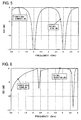
- Fig. 2 shows the result of a simulation of the frequency response of pass characteristics (S21) of the bias circuit 100 when the switch 7 is in the off state, where the first frequency f 1 is 1 GHz and the second frequency f 2 is 2 GHz.
- Shown in Fig. 2 is the result of the simulation of the pass characteristics (S21) calculated when a port P1 and a port P2 are connected to a 50-ohm system, where the port P1 is the input terminal of the bias circuit 100 shown in Fig. 1 and the port P2 is the output terminal of the bias circuit 100.
- the signal of 1 GHz passed with little loss whereas the signal of 2 GHz passed with a loss of nearly 30 dB.
- the calculation in the simulation was performed with the assumption that the switch 7 is an ideal switch that has zero loss in the on state and infinite isolation in the off state. While a case where the ideal switch is used will be described below, a frequency response relating to the amplitude and phase of the switch must be considered in the actual design, as well as characteristics of other components.
- the first reactance means 2 and the second reactance means 3 of the bias circuit 100 are implemented by transmission lines in such a manner that the sum of the electrical lengths is 90 degrees at the first frequency f 1 , the position where is open-circuited at the second frequency f 2 when the second connection point 220 is short-circuited while the switch 7 is in the off state will be between the bias point 800 and the second connection point 220, under condition of f 1 ⁇ f 2 .
- the first connection point 210 is provided at the open-circuited position, which is one of the features of the bias circuit of the present invention.
- the first connection point 210 to which the switch 7 connects is at a position such that the impedance is sufficiently large at the second frequency f 2 , as viewed from the first connection point 210 toward the second reactance means 3.
- the line length of the second reactance means 3, which is the transmission line between the first connection point 210 and the second connection point 220, may be ⁇ 2 /4.
- the line length of the reactance means 2 will be ( ⁇ 1 /4 - ⁇ 2 /4).
- the total impedance Z 12 + Z 22 + Z c2 at the second frequency f 2 (f 1 ⁇ f 2 ) when the switch 7 is in the off state is not sufficiently large unless the second frequency f 2 is an odd multiple of the first frequency f 1 .
- the impedance at the second frequency f 2 as viewed from the first connection point 210 toward the second reactance means 3 is sufficiently large. That is, Z 22 +Z c2 is sufficiently large.
- the switch 7 is turned on at the second frequency f 2 to effect the operation of the bias circuit 100.
- the total impedance Z 12 + Z 32 of the first reactance means 2 and the third reactance means 8 viewed from the bias point 800 at the second frequency f 2 is sufficiently large.
- the impedance Z 32 of the third reactance means 8 is set to a value such that the total impedance Z 12 + Z 32 at the second frequency f 2 , which is the impedance as viewed from the bias point 800 toward the bias circuit 100 while the switch 7 is in the on state, is sufficiently large.
- the bias circuit 100 including the first reactance means 2, the second reactance means 3, the DC circuit 5 and the DC power supply 6 can be prescinded from the AC circuit at the second frequency f 2 in terms of alternating current.
- the third reactance means 8 is implemented by an open-circuited transmission line, the sum of the electrical lengths of the first reactance means 2 and the third reactance means 8 may be designed to be 180 degrees, for example, at the second frequency f 2 .
- the line length of the third reactance means 8 will be (2p x ⁇ 2 /4 - ( ⁇ 1 /4 - ⁇ 2 /4)), where p is a positive integer and the symbol x denotes multiplication.
- the line length of the first reactance means 2 may be chosen to be ⁇ 2 /4 and the line length of the third reactance means 8 may chosen to be ⁇ 2 /4.
- Fig. 3 shows the frequency response of pass characteristics (S21) of the bias circuit 100 when the switch is in the on state. As shown in Fig. 3 , the bias circuit 100 allowed a signal of 2 GHz to pass through with little loss.
- the bias circuit 100 including the first reactance means 2, the second reactance means 3, the DC circuit 5 and the DC power supply 6 can be prescinded from the AC circuit at two different frequencies in terms of alternating current by switching the state of the switch 7 (between the on and off states).
- the dual-band bias circuit 100 has been described above. Consider a design that requires two different frequencies, 1 GHz and 1.2 GHz. If a signal loss of up to approximately 3 dB is to be allowed in the bias circuit 100 on the basis of the frequency response of pass characteristics (S21) of the bias circuit 100 shown in Fig. 2 , the bias circuit 100p having a conventional configuration can sufficiently achieve the design target. However, the frequency responses of pass characteristics (S21) of conventional bias circuits in general do not necessarily show low-loss in a wide band as shown in Fig. 2 . In addition, conventional bias circuits do not necessarily achieve the purpose of operating at each of not only adjacent two frequency bands but also two arbitrary frequency bands.
- the bias circuit 100 according to the first embodiment is capable of operating at each of two bands regardless of the distance between the two bands by setting a position of the first connecting part 210 and switching the state of the switch 7.
- the effect described above is applied to not only the dual-band bias circuit 100 but also bias circuits in general according to the present invention.
- the first connection point 210 to which the switch 7 connects is provided at a position such that the impedance at the second frequency f 2 as viewed from the connection point 210 toward the second reactance means 3 is sufficiently large.
- the line length of the second reactance means 3 can take on multiple design values in this way, any of the line lengths can be selected.
- the position of the first connection point 210 can be set in accordance with a frequency band required by a design.
- the reactance means is not limited to a transmission line; it may be implemented by a lumped-parameter element.
- the third reactance means 8 can be easily implemented by a lumped-parameter element because the third reactance means 8 is used only at a single frequency.
- the bias circuit can be reduced in size by using lumped-parameter elements.
- a bias circuit having the same configuration may also be provided on the output terminal side of the FET 180.
- Basic operation of the bias circuit is the same as that of the bias circuit provided on the input terminal side of the FET 180 and therefore the description of which will be omitted.
- Fig. 4 shows a bias circuit 200 according to a second embodiment of the present invention.
- the other end of the third reactance means 8 (the end to which the switch 7 is not connected) is grounded via a second capacitive means 9.
- the bias circuit 200 including the first reactance means 2, the second reactance means 3, the DC circuit 5 and the DC power supply 6 can be prescinded from the AC circuit at each of two frequencies in terms of alternating current by switching the state of the switch 7.
- a bias circuit capable of operating at each of two bands can be implemented.
- the line length of the third reactance means 8 can be chosen to be ((2p - 1 ) x ⁇ 2 /4 - ( ⁇ 1 /4 - ⁇ 2 /4)), where p is a positive integer.
- the line length of the third reactance means 8 can be reduced in some cases by a short circuit in terms of alternating current of the other end of the third reactance means 8.
- the line length of the third reactance means 8 can be only approximately 20 degrees in terms of electrical length at the second frequency f 2 .
- the line length of the third reactance means 8 at the second frequency f 2 needs to be approximately 103 degrees.
- Fig. 5 shows the result of a simulation of the frequency response of the pass characteristics (S21) of the bias circuit 200 when the switch 7 is in the off state, where the first frequency f 1 is 1 GHz and the second frequency f 2 is 3.8 GHz.
- Fig. 6 shows the result of a simulation of the frequency response of the pass characteristics (S21) of the bias circuit 200 when the switch is in the on state. Shown in Figs. 5 and 6 are the results of simulations of the pass characteristics (S21) calculated for a case where the port P and the port P2 are connected to a 50-ohm system, where the port P1 is the input terminal of the bias circuit 200 shown in Fig. 4 and the port P2 is the output terminal of the bias circuit 200. As shown in Fig.
- the signal of 1 GHz passed with little loss through the bias circuit 200 in which the switch 7 is in the off state whereas the signal of 3.8 GHz passed with a loss.
- the signal of 3.8 GHz passed with little loss through the bias circuit 200 in which the switch 7 is in the on state.
- the bias circuit operates at each of two frequencies in the first and second embodiments, the bias circuit operates at more frequencies in third, fourth, and fifth embodiments based on a similar idea.
- the reactance of the third reactance means 8 is changed in accordance with an AC frequency so that impedance as viewed from the bias point 800 toward a bias circuit becomes sufficiently large when the first connection point 210 is open-circuited at multiple AC frequencies such as odd multiples of a first AC frequency f 1 .
- a configuration of the bias circuit in the third embodiment enables adjustment of the reactance of the third reactance means 8 affected by a design value of "sufficiently large impedance".
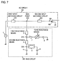
- Fig. 7 shows the third embodiment of the present invention.
- the bias circuit 300 according to the third embodiment uses a variable reactance means capable of changing reactance values, in place of the third reactance means 8 in the bias circuit 200 in the second embodiment.
- the variable reactance means may be a variable capacitor capable of changing its capacitance of which.
- the bias circuit 300 capable of operating at each of q + 1 bands can be implemented.
- q is an integer greater than or equal to 2.
- variable reactance means whose reactance value can be changed may also be used as the third reactance means 8 in the bias circuit 100 in the first embodiment.
- the third reactance means 8 may be implemented by one-input q-output switches 71 and 72, which are selector switches, and q reactance elements 81 1 , ..., 81 q capable of being connected to the selector switches.
- the q reactance elements 81 1 , ..., 81 q are arranged in parallel.
- One end of the switch 71 is connected to the first connection point 210 and one end of switch 72 is connected to the second capacitive means 9. The other ends of the switch 71 and the switch 72 are switched to select the same reactance element.
- q reactance values can be obtained by switching the states of the switches 71 and 72.
- each of the other ends (ends that are not connected to the switch 71) of some or all of q reactance elements 81 1 , ..., 81 q may be connected to a second capacitive means without providing the switch 72, although not necessarily effective in reducing the size of the entire circuit.
- at least one reactance element may be capable of being connected to a second capacitive means.
- the switch 71 may be implemented as a selector switch that can be placed in the state in which the switch 71 is not connected to any of the reactance elements.
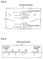
- a combination of switches and reactance elements may be used as shown in Fig. 9 or 10 .
- q reactance elements 81 1 , ..., 81 q and q - 1 switches 7 2 , ..., 7 q are alternately cascade-connected. That is, one end of the reactance element 81 1 located at one end of the cascade-connected reactance elements is connected to the switch 7 and the other end (the end to which the switch 7 is not connected) of the reactance element 81 1 is connected to one end of the switch 7 2 .
- One end of the reactance element 81 x is connected to the other end of the switch 7 x and the other end of the reactance element 81 x is connected to one end of the switch 7 x+1 .
- x 2, 3, ..., q - 1.
- One end of the reactance element 81 q at the other end of the cascade-connected reactance elements is connected to the other end of the switch 7 q and the other end of the reactance element 81 q is connected to the second capacitive means 9.
- the reactance means can be designed so that switches 7 2 , ..., 7 y are turned on and the switch 7 y+1 is turned off with regard to the (y + 1)-th frequency f y+1 .
- y 1
- the switch 7 2 is turned off.
- q reactance elements 81 1 ,.., 81 q and q - 1 switches 18 2 , ..., 18 q are alternately cascade-connected.
- One end of the reactance element 81 1 located at one end of the cascade-connected reactance elements is connected to the switch 7.
- One end of the switch 18 x is connected to the other end of the reactance element 81 x-1 , and the other end of the switch 18 x is capable of being connected to any of one end of the reactance element 81 x and one end of a second capacitive means 19 x .
- x 1, 2, 3, ..., q.
- the other end of the reactance element 81 q is connected to the second capacitive means 9.
- Fig. 11 shows a fourth embodiment of the present invention.
- the fourth embodiment is an expanded version of the second embodiment in which the idea for operating at each of two bands described with respect to the second embodiment is expanded to operate at each of (n + 1) bands.
- multiple reactance means are provided.
- a bias circuit 400 shown in Fig. 11 has a circuit part including the first reactance means 2 and n second reactance means 3 1 , ..., 3 n cascade-connected.
- one end of the first reactance means 2 is connected to the bias point 800 and the other end of the first reactance means 2 is connected to one end of the second reactance means 3 n .
- the other end (the end to which the first reactance means 2 is not connected) of the second reactance means 3 n is connected to one end of the second reactance means 3 n-1 .
- the other end (the end to which the second reactance means 3 n is not connected) of the second reactance means 3 n-1 is connected to one end of the second reactance means 3 n-2 .
- Such connection is repeated to form a cascade connection and one end of the second reactance means 3 2 (the end to which second reactance means 3 3 is not connected) is connected to one end of the second reactance means 3 1 .
- the other end of the second reactance means 3 1 is connected to the capacitive means 4.
- a third reactance means 8 n is connected to a connection point 21 n between the first reactance means 2 and the second reactance means 3 n via a switch 7 n .
- a third reactance means 8 x is connected to a connection point 21 x between the second reactance means 3 x+1 and the second reactance means 3 x via a switch 7 x .
- x n - 1, n - 2, ..., 1.
- Second capacitive means 9 1 , ..., 9 n one end of which is grounded is connected to one end of each third reactance means 8 1 , ..., 8 n (the end to which a switch is not connected).
- the n second reactance means 3 1 , ..., 3 n are not limited to the same type.
- some of n second reactance means 3 1 , ..., 3 n may be implemented as transmission lines and the others may be implemented by lumped-parameter elements at designer's discretion.
- the DC circuit 5 and the DC power supply 6 can be prescidned in terms of alternating current with regard to each of at least (n + 1) frequencies by switching the state of any of the switches 7 1 , ..., 7 n .
- the bias circuit 400 is capable of operating at each of at least (n + 1) bands.
- a bias circuit capable of operating at each of (n+1) bands for example, if the DC circuit 5 and the DC power supply 6 are to be prescinded in terms of alternating current with regard to the (m + 1)-th frequency, only switch 7 m is turned on, where m is an integer greater than or equal to 1. At a first frequency, all switches 7 1 , ..., 7 n are tuned off.
- the position at which the switch 7 m is to be connected is chosen to be such that the impedance as viewed from the position toward second reactance means 3 1 , ..., 3 m at the (m + 1)-th frequency is sufficiently large.
- turning on one switch does not necessarily mean that the bias circuit 400 capable of operating at each of (n + 1) bands is formed.
- the first reactance means 2 and the second reactance means 3 1 , ..., 3 n are implemented by transmission lines, similar biasing can also be achieved for an odd multiple of the frequency of an AC signal when only a particular switch is turned on.
- the number of switches turned on in the fourth embodiment is not limited to one.
- the impedance as viewed from the connection point of the switch 7 x toward the capacitive means 4 can be sufficiently large at frequencies other than (n + 1) bands, depending on the design values of third reactance means connected to the turned-on switches other than the switch 7 x .
- turning on the switch 7 x closest to the bias point 800 among the turned on switches means that the impedance as viewed from the connection point 21 x to which the switch 7 x is connected toward the capacitive means 4 is made sufficiently large; turning on one or more switches appropriately farther from the bias point 800 than the switch 7 x means that the design value or values of third reactance means connected to the turned-on switch or switches determine an operating frequency that can be biased accordingly.
- each of one ends of the third reactance means 8 1 , ..., 8 n is grounded via the second capacitive means 9 1 , ..., 9 n in the fourth embodiment
- the present invention is not limited to such an embodiment.
- One end of at least one of the third reactance means 8 1 , ..., 8 n may be connected to one end of a second capacitive means the other end of which is grounded.
- at least one of the third reactance means 8 1 , ..., 8 n may comprise a transmission line and one end of at least one of the third reactance means that comprises the transmission line may be an open-circuited end of the transmission line.
- Fig. 12 shows a fifth embodiment of the present invention.
- a bias circuit 500 shown in Fig. 12 has a circuit part in which the first reactance means 2 and n second reactance means 3 1 , ..., 3 n are cascade-connected as in the fourth embodiment.
- a fourth reactance means 21 and n fifth reactance means 31 1 , ..., 31 n are also cascade-connected.
- one end of the fourth reactance means 21 is open-circuited and the other end is connected to one end of the fifth reactance means 31 n .
- the other end of the fifth reactance means 31 n (the end to which the fourth reactance means 21 is not connected) is connected to one end of the fifth reactance means 31 n-1 .
- the other end of the fifth reactance means 31 n-1 (the end to which the fifth reactance means 31 n is not connected) is connected to one end of the fifth reactance means 31 n -2. Such connection is repeated to form a cascade connection and the other end of the fifth reactance means 31 2 (the end to which fifth reactance means 31 3 is not connected) of the fifth reactance means 31 2 is connected to one end of the fifth reactance means 31 1 .
- the other end of the fifth reactance means 31 1 is open-circuited.
- the fourth reactance means 21 and the fifth reactance means 31 1 for example, comprise a transmission line and each of one ends of the fourth reactance means 21 and the fifth reactance means 31 1 is the open-circuited end of the transmission line.
- connection point 21 n between the first reactance means 2 and the second reactance means 3 n is connected with a connection point 22 n between the fourth reactance means 21 and the fifth reactance means 31 n via the switch 7 n .
- connection point 21 x between the second reactance means 3 x+1 and the second reactance means 3 x is connected with a connection point 22 x between the fifth reactance means 31 x+1 and the fifth reactance means 31 x via the switch 7 x .
- x n-1, n-2, ..., 1.
- the second reactance means are associated with the fifth reactance means in a one-to-one correspondence.
- n second reactance means 3 1 , ..., 3 n and n fifth reactance means 31 1 , ..., 31 n are not limited to the same types.
- some of the n second reactance means 3 1 , ..., 3 n and some of n fifth reactance means 31 1 , ..., 31 n may be implemented as transmission lines and the others may be implemented by lumped-parameter elements at designer's discretion.
- the fourth reactance means 21 and n fifth reactance means 31 1 , ..., 31 n are made to have the same reactance values as those of their associated first reactance means 2 and second reactance means 3 1 , ...,3 n , respectively.
- the position the switch 7 m is connected that is, the position of the connection point 21 m is chosen to be such that the impedance as viewed from the connection point 21 m toward the second reactance means 3 1 , ..., 3 m is sufficiently large.
- the impedance as viewed from the connection point 22 m (or connection point 21 m ) toward the fifth reactance means 31 1 , ..., 31 m will be sufficiently small. Accordingly, the impedance as viewed from the bias point 800 toward the first reactance means 2 will be sufficiently large.
- connection point 21 m to the bias point 800 The electrical length from the connection point 21 m to the bias point 800 is equal to the electrical length from the connection point 21 m to the open-circuited end of the fourth reactance means 21. Therefore, when the impedance at the open-circuited end of the fourth reactance means is infinite, the DC circuit 5 and the DC power supply 6 can be prescinded from the AC circuit in terms of alternating current.
- While one end of the fifth reactance means 31 1 (the end to which the fifth reactance means 31 2 is not connected) is open-circuited herein, the end may be grounded via second capacitive means such as a capacitor.
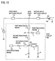
- Fig. 13 shows a sixth embodiment of the present invention.
- sixth reactance means 131 and 132 and a switch 14 are added to the bias circuit 100 of the first embodiment.
- the sixth reactance means 131 and 132 are not limited to means of the same type. For example one of them may be implemented as a transmission line and the other as a lumped-parameter element.
- the sixth reactance means 131 is connected with the capacitive means 4, the DC circuit 5, and second reactance means 3 at the second connection point 220.
- the switch 14 is in the off state.
- the reactance value of the sixth reactance means 131 is designed so that the second connection point 220 is short-circuited at the second frequency f 2 .
- the sixth reactance means 131 may be implemented by a transmission line having a line length of ⁇ 2 /4.
- the switch 14 is turned on.
- the reactance value of the sixth reactance means 132 is designed so that the second connection point 220 is short-circuited at the first frequency f 1 .
- the line length of the sixth reactance means 131 is ⁇ 2 /4
- the sixth reactance means 132 may be implemented by a transmission line having a line length of ( ⁇ 1 /4 - ⁇ 2 /4).
- the second connection point 220 can be short-circuited for AC signals of different frequencies even if the capacitance of the capacitive means 4 is not sufficiently large.
- a reactance is provided by a reactance providing means to the open position at frequency f b so that the impedance as viewed from the bias point 800 toward the bias circuit becomes sufficiently large.
- the reactance providing means may provide a reactance to open positions that vary depending on AC frequencies.
- Condition 1 reactance at an AC frequency f r may be designed such that the impedances as viewed from open positions at the AC frequencies other than the AC frequency f r toward the reactance providing means are sufficiently large;
- Condition 2 The Condition 1 holds for each AC frequency;
- Condition 3 at each AC frequency, the impedance as viewed from the bias point 800 toward the bias circuit is sufficiently large; are satisfied.
- the reactance of first reactance means and the reactance of each of second reactance means are also designed so that the conditions given above are satisfied. In designing, it must be kept in mind that the open position at an AC frequency f r is possibly affected by the reactances provided to the open positions at the AC frequencies other than the AC frequency f r .
- the reactance providing means may be made connectable to each open position via one switch, and the switch may be turned on and off in accordance with an AC frequency.
- the connection point to which the switch that is closest to the bias point is connected among the switches turned on is the open position at an AC frequency when the switch is turned on.
- the impedance as viewed from the open position toward the capacitive means 4 is sufficiently large and the flexibility of the configuration and design of the reactance providing means is high.
- the bias circuit 400 in which the reactance providing means includes n third reactance means 8 1 , ..., 8 q .
- circuit part X including second reactance means 3 1 , ..., 3 m , capacitive means 4, a DC circuit 5, and a DC power supply 6 and circuit part Y including third reactance means 8 m and second capacitive means 9 m .
- the impedance Z P 1/(1/Z X + 1/Z Y ) of the parallel resonant circuit is determined in effect by the impedance Z Y of circuit part Y
- the reactance means does not provide a reactance between the bias point and the connection point 21 m which is an open position. Accordingly, when only the switch 7 m is in the on state, the impedance as viewed from the bias point 800 toward the bias circuit 400 may be considered to be the combined impedance of the impedance of the first reactance means 2, the impedance of each second reactance means 3 m+1 , ..., 3 n , and the impedance Z Y of circuit part Y.
- the reactance providing means in the bias circuit described above can be configured as described with respect to the third embodiment.
- Bias circuits of the present invention are not limited to the embodiments described above. Modifications are permitted to be made as appropriate according to the usage unless departed from the inventive concept.
- Fig. 14 illustrates a low-loss multiband matching circuit 900 described in literatures Non Patent Literature 1 and 2 listed above.
- a multiband matching circuit 900 capable of operating at each of two bands is illustrated for convenience of illustration of a combined use with the bias circuit of the first embodiment described above.
- the multiband matching circuit 900 comprises a main matching block 910, a delay circuit 920 one end of which is connected to the main matching block 910, a sub matching block 930, and a switch 940 connected between the other end of the delay circuit 920 and one end of the sub matching block 930.
- one end of the main matching block 910 (the end to which the delay circuit 920 is not connected) is connected to the FET 180 in Fig.
- the multiband matching circuit 900 matches the impedance Z(f) as viewed from a port 952 toward the FET 180 in a signal band to the impedance Z 0 of the load (AC signal source 1).
- Impedance matching at a frequency f 1 will be described first: In this case, the switch 940 is turned off. For example, a signal input through the port 951 passes only through the main matching block 910 and the delay circuit 920 and travels to the port 952. It is assumed here that the main matching block 910, which may have any configuration, matches impedance Z(f 1 ) to impedance Z 0 at frequency f 1 . Also, it is assumed that the delay circuit 920 is a transmission line which has the characteristic impedance Z 0 . Accordingly, the impedance value as viewed from the port 951 toward the multiband matching circuit 900 is Z 0 . That is, the multiband matching circuit 900 establishes impedance matching throughout the circuit at frequency f 1 .
- impedance matching at frequency f 2 will be described next.
- the switch 940 is turned on.
- the main matching block 910 operates as an impedance converter at frequency f 2 as well. Accordingly, the impedance as viewed from a point 953 toward the port 952 will be impedance Z L '(f 2 ) converted from the impedance Z L (f 2 ) of the port 952.
- the impedance value as viewed from the port 951 toward the multiband matching circuit 900 can be converted to Z 0 on the principle of single stub matching. That is, the multiband matching circuit 900 can establish impedance matching throughout the circuit at frequency f 2 as well.
- the multiband matching circuit 900 can be designed to operate as a matching circuit at each of frequencies f 1 and f 2 . That is, the multiband matching circuit 900 functions as a matching circuit for two frequency bands by switching the state (on/off) of a single switch.
- Fig. 15 shows a combined use of the multiband matching circuit 900 and the bias circuit 100 capable of operating at each of two bands according to the first embodiment described above. It can be said that the combined use is a variation of the first embodiment, in which the second input matching circuit 320 of the first embodiment is omitted and the first input matching circuit 310 is replaced with the multiband matching circuit 900.
- both of switch 7 and switch 940 are turned off at a first frequency f 1 and are turned on at a second frequency f 2 .
- impedance matching can be accomplished by the main matching block 910 and the delay circuit 920.
- impedance matching can also be accomplished by taking into consideration the existence of first reactance means 2 and third reactance means 8 in terms of alternating current, as well as the main matching block 910, delay circuit 920 and sub matching block 930.
- an amplifier circuit capable of operating at each of (n+1) bands can be implemented by combining the multiband matching circuit capable of operating at each of (n+1) bands disclosed in the literatures listed above with any of the third, fourth and fifth embodiment of the present invention.
- bias circuits can operate as a bias circuit for only a particular frequency but cannot operate at each of multiple frequency bands.
- Patent Literature 2 listed above of operating a bias circuit at each of multiple frequency bands has a problem that the entire bias circuit increases in size because the method basically requires the bias circuit shown in Fig. 16 for each frequency as the number of bands.
- Patent Literature 3 listed above of operating at each of multiple frequency bands has a similar problem because it needs multiple bias circuits prepared as described in the literature.
- Bias circuits as many as the number of bands that requires bias circuits may be provided in order to operate at each of the multiple frequency bands.
- the size of the circuits unrealistically increases in consequences.
- impedance as viewed from a bias point toward a bias circuit can be made sufficiently large by a reactance provided with respect to different AC frequencies by a reactance providing means provided in the bias circuit as can be seen from the description of the embodiments described above, and therefore a DC voltage can be supplied to an AC circuit without affecting an AC signal transmitted in the AC circuit.
- a bias circuit capable of operating at each of multiple frequency bands can be realized. Because multiple frequency bands can be handled by a single bias circuit, it is not necessary to provide as many bias circuits as the number of operating frequency bands.
Landscapes
- Engineering & Computer Science (AREA)
- Power Engineering (AREA)
- Waveguide Connection Structure (AREA)
- Amplifiers (AREA)
- Microwave Amplifiers (AREA)
Claims (16)
- Biasschaltung mit einem Biaspunkt (800), der mit einer Wechselstromschaltung (120) verbunden und dazu ausgelegt ist, auf jeder von zumindest zwei Betriebsfrequenzen betrieben zu werden, wobei die Impedanz an jeder von jenen Betriebsfrequenzen am Biaspunkt (800), wie zur Biasschaltung (100) hin gesehen, ausreichend groß ist, um zu verhindern, dass ein Wechselstromsignal der jeweiligen Betriebsfrequenz am Biaspunkt (800) von der Biasschaltung (100) beeinträchtigt wird, mit:einer ersten Reaktanzeinrichtung (2), deren eines Ende mit der Wechselstromschaltung (120) verbunden ist, wobei das eine Ende den Biaspunkt (800) definiert;einer kapazitiven Einrichtung (4), deren eines Ende geerdet ist;einem Gleichstromschaltungsteil (10), das imstande ist, eine Gleichspannung zuzuführen, wobei das Gleichstromschaltungsteil (10) mit dem anderen Ende der kapazitiven Einrichtung (4) verbunden ist; undeiner oder mehreren zweiten Reaktanzeinrichtungen (3, 31-3n);dadurch gekennzeichnet, dassdie Biasschaltung ferner zumindest einen Schalter (7, 71, 71-7n) und einen Reaktanzblock umfasst, der eine oder mehrere Reaktanzeinrichtungen (8, 811-81q, 81-8n, 21, 311-31n) einschließt;die eine oder mehreren zweiten Reaktanzeinrichtungen (3, 31-3n) zwischen dem anderen Ende der ersten Reaktanzeinrichtung (2) und dem anderen Ende der kapazitiven Einrichtung kaskadengeschaltet sind;jeder Verbindungspunkt (210, 211-21n) von benachbarten zwei Reaktanzeinrichtungen, der zu der ersten und zweiten Reaktanzeinrichtung (2, 3, 31-3n) gehört, mit zumindest einer Reaktanzeinrichtung in dem Reaktanzblock über einen entsprechenden des zumindest einen Schalters verbunden ist;jeder Verbindungspunkt (210, 211-21q) hinsichtlich des Wechselstroms, wie zur kapazitiven Einrichtung (4) hin gesehen, in Abhängigkeit von einer entsprechenden der zumindest zwei Betriebsfrequenzen offen ist oder nicht; undeine Gesamtimpedanz der Biasschaltung (100) ausschließlich eines Schaltungsteils jenseits eines Verbindungspunkts, der dem Biaspunkt (800) unter dem einen oder den mehreren Verbindungspunkten in offener hinsichtlich des Wechselstroms am nächsten ist, wobei das Schaltungsteil das Gleichstromschaltungsteil (10) einschließt, ausreichend groß ist, um zu verhindern, dass das Wechselstromsignal der jeweiligen Betriebsfrequenz am Biaspunkt (800) von der Biasschaltung (100) auf jeder der zumindest zwei Betriebsfrequenzen beeinträchtigt wird.
- Biasschaltung nach Anspruch 1, wobei:jeder des zumindest einen Schalters (7, 71, 71-7n) dazu ausgelegt ist, selektiv zwischen einem Ein-Zustand, der den jeweiligen Verbindungspunkt mit der zumindest einen Reaktanzeinrichtung in dem Reaktanzblock verbindet, und einem Aus-Zustand, der den jeweiligen Verbindungspunkt von jeglicher Reaktanzeinrichtung im Reaktanzblock trennt, umgeschaltet zu werden, wobei jeder Zustand des Schalters oder der Schalter einer anderen der zumindest zwei Betriebsfrequenzen entspricht; undder Verbindungspunkt, der dem Biaspunkt (800) unter einem oder mehreren Verbindungspunkten, die mit einem Schalter (7, 71, 71-7n) in einem Ein-Zustand verbunden sind, am nächsten ist, hinsichtlich des Wechselstroms auf der jeweiligen Betriebsfrequenz offen ist.
- Biasschaltung nach Anspruch 2, wobei:die Anzahl der einen oder mehreren zweiten Reaktanzeinrichtungen (3, 31-3n) eins beträgt;die Anzahl des zumindest einen Schalters (7, 71, 71-7n) eins beträgt;die Anzahl der Reaktanzeinrichtung in dem Reaktanzblock eins beträgt; undder Aus-Zustand des einen Schalters (7) einer ersten Frequenz f1 der zumindest zwei Betriebsfrequenzen entspricht, wohingegender Ein-Zustand einer Frequenz entspricht, die sich von der Frequenz f1 der zumindest zwei Betriebsfrequenzen unterscheidet.
- Biasschaltung nach Anspruch 3, wobei:q eine vorgegebene ganze Zahl bezeichnen soll, die größer oder gleich 2 ist,die Reaktanzeinrichtung (8) in dem Reaktanzblock dazu ausgelegt ist, ihren Reaktanzwert unter q Reaktanzwerten zu ändern.
- Biasschaltung nach Anspruch 3, wobei:q eine vorgegebene ganze Zahl bezeichnen soll, die größer oder gleich 2 ist,die Reaktanzeinrichtung (8) in dem Reaktanzblock q Reaktanzelemente (811-81q) umfasst; undder eine Schalter (71) dazu ausgelegt ist, den Verbindungspunkt zwischen der ersten Reaktanzeinrichtung (2) und der zweiten Reaktanzeinrichtung (3) mit einem Ende von irgendeinem der q Reaktanzelemente (811-81q) zu verbinden, wodurch er eine jeweilige der zumindest zwei Betriebsfrequenzen definiert, die sich von der ersten Frequenz f1 unterscheidet.
- Biasschaltung nach Anspruch 3, wobei:q eine vorgegebene ganze Zahl bezeichnen soll, die größer oder gleich 2 ist,die Reaktanzeinrichtung (8) in dem Reaktanzblock q Reaktanzelemente (811-81q) und q-1 Schalter (72-7q), die jeweils einen Auswahlschalter definieren, umfasst;das andere Ende des einen Schalters (7) mit einem Ende eines ersten (811) der q Reaktanzelemente (811-81q) verbunden ist; undx jede ganze Zahl bezeichnen soll, die größer oder gleich 1 und kleiner oder gleich q-1 ist,ein Ende eines x-ten der q-1 Auswahlschalter (72-7q) mit dem andere Ende eines x-ten der q Reaktanzelemente (811-81q) verbunden ist und das andere Ende des x-ten Auswahlschalters mit einem Ende eines (x+1)-ten der q Reaktanzelemente (811-81q) verbunden ist.
- Biasschaltung nach irgendeinem der Ansprüche 1 bis 4, wobei:das andere Ende der zumindest einen Reaktanzeinrichtung in dem Reaktanzblock mit einem Ende einer zweiten kapazitiven Einrichtung (9, 91-9n) verbunden ist, deren anderes Ende geerdet ist.
- Biasschaltung nach Anspruch 5; wobei:die Biasschaltung ferner einen zweiten Schalter (72) umfasst; undein Ende des zweiten Schalters (72) mit einem Ende einer zweiten kapazitiven Einrichtung (9) verbunden ist, deren anderes Ende geerdet ist, und das andere Ende des zweiten Schalters (72) selektiv mit dem anderen Ende jenes einen der q Reaktanzelemente (811-81q) verbunden ist, dessen eines Ende mit dem einen Schalter (71) verbunden ist.
- Biasschaltung nach Anspruch 6, wobei:das andere Ende des q-ten der q Reaktanzelemente (811-81q) mit einem Ende einer zweiten kapazitiven Einrichtung (9) verbunden ist, deren anderes Ende geerdet ist.
- Biasschaltung nach Anspruch 6, wobei:die Biasschaltung ferner q-1 zweite kapazitive Einrichtungen (192-19q) umfasst;ein Ende von jeder der zweiten kapazitiven Einrichtungen (192-19q) geerdet ist; unddas andere Ende des x-ten der q-1 Auswahlschalter (72-7q) selektiv mit dem anderen Ende einer entsprechenden der q-1 zweiten kapazitiven Einrichtungen (192-19q) auf der jeweiligen Betriebsfrequenz verbunden ist.
- Biasschaltung nach Anspruch 2, wobei:n eine vorgegebene ganze Zahl bezeichnen soll, die größer oder gleich 2 ist, und m jede ganze Zahl bezeichnen soll, die größer oder gleich 1 und kleiner oder gleich n ist,die Anzahl der einen oder mehreren zweiten Reaktanzeinrichtungen (3, 31-3n) n ist;die Anzahl des zumindest einen Schalters (7, 71, 71-7n) n ist;der Reaktanzblock n dritte Reaktanzeinrichtungen (81-8n) umfasst;jeder Verbindungspunkt (211-21n) mit einer entsprechenden der n dritten Reaktanzeinrichtungen (81-8n) über einen entsprechenden der n Schalter (71-7n) verbunden ist;der Fall aller n Schalter (71-7n), die in einem Aus-Zustand platziert sind, einer ersten Frequenz f1 der zumindest zwei Betriebsfrequenzen entspricht; undder Fall zumindest eines der n Schalter (71-7n), die in einem Ein-Zustand platziert sind, einer (m+1)-ten Frequenz fm+1 der zumindest zwei Betriebsfrequenzen entspricht.
- Biasschaltung nach Anspruch 11, wobei:das andere Ende zumindest einer der n dritten Reaktanzeinrichtungen (81-8n) mit einem Ende einer zweiten kapazitiven Einrichtung (91-9n) verbunden ist, deren anderes Ende geerdet ist.
- Biasschaltung nach Anspruch 11, wobei:zumindest eine der n dritten Reaktanzeinrichtungen (81-8n) eine Übertragungsleitung umfasst und das andere Ende zumindest einer der n dritten Reaktanzeinrichtungen (81-8n), die die Übertragungsleitung umfasst, ein Leerlaufende der Übertragungsleitung ist.
- Biasschaltung nach Anspruch 2, wobei:n eine vorgegebene ganze Zahl bezeichnen soll, die größer oder gleich 2 ist, und k jede ganze Zahl bezeichnen soll, die größer oder gleich 1 ist,die Anzahl der einen oder mehreren zweiten Reaktanzeinrichtungen (3, 31-3n) n ist;die Anzahl des zumindest einen Schalters (7, 71, 71-7n) n ist;der Reaktanzblock eine vierte Reaktanzeinrichtung (21) und n fünfte Reaktanzeinrichtungen (311-31n) umfasst;die fünften Reaktanzeinrichtungen (311-31n) kaskadengeschaltet sind;eine fünfte Reaktanzeinrichtung γ (31n) als die fünfte Reaktanzeinrichtung an einem Ende der kaskadengeschalteten n fünften Reaktanzeinrichtungen (311-31n) definiert ist und eine fünfte Reaktanzeinrichtung θ (311) als die fünfte Reaktanzeinrichtung an deren anderen Ende definiert ist,ein Ende der fünften Reaktanzeinrichtung γ (31n), das nicht mit irgendeiner der anderen fünften Reaktanzeinrichtungen verbunden ist, mit einem Ende der vierten Reaktanzeinrichtung (21) verbunden ist;ein Verbindungspunkt (21n) der ersten Reaktanzeinrichtung (2) und einer der n zweiten Reaktanzeinrichtungen (31-3n) mit einem Verbindungspunkt (22n) der fünften Reaktanzeinrichtung γ (31n) und der vierten Reaktanzeinrichtung (21) über einen entsprechenden der n Schalter (71-7n) verbunden ist;jeder Verbindungspunkt (211-21n-1), ausschließlich des Verbindungspunkts (21n) der ersten Reaktanzeinrichtung (2) und einer der n zweiten Reaktanzeinrichtungen (31-3n), mit einem entsprechenden von Verbindungspunkten (221-22n-1) von benachbarten zwei der kaskadengeschalteten n fünften Reaktanzeinrichtungen (311-31n) über einen entsprechenden der n Schalter (71-7n) verbunden ist;die n zweiten Reaktanzeinrichtungen (31-3n) den n fünften Reaktanzeinrichtungen (311-31n) in einer Eins-zu-Eins- Entsprechung zugeordnet sind;die vierte Reaktanzeinrichtung (21) den gleichen Reaktanzwert wie denjenigen der ersten Reaktanzeinrichtung (2) hat;jede der n fünften Reaktanzeinrichtungen (311-31n) den gleichen Reaktanzwert wie denjenigen eines entsprechenden der n zweiten Reaktanzeinrichtungen (31-3n) hat;der Fall, dass alle n Schalter (71-7n) in einem Aus-Zustand platziert sind, einer Frequenz der zumindest zwei Betriebsfrequenzen entspricht, die gleich dem (2k-1)-Fachen einer ersten Frequenz f1 ist; undjener Fall, dass nur einer der n Schalter (71-7n) in einem Ein-Zustand platziert ist, einer Frequenz der zumindest zwei Betriebsfrequenzen entspricht, die gleich dem 2k-Fachen der ersten Frequenz f1 ist.
- Biasschaltung nach Anspruch 14, wobei:ein Ende der fünften Reaktanzeinrichtung θ (311), das nicht mit irgendeiner der anderen fünften Reaktanzeinrichtungen verbunden ist, mit einem Ende einer zweiten kapazitiven Einrichtung verbunden ist, deren anderes Ende geerdet ist.
- Biasschaltung nach Anspruch 14, wobei:die fünfte Reaktanzeinrichtung θ (311) eine Übertragungsleitung umfasst; undein Ende der fünften Reaktanzeinrichtung θ (311), die nicht mit irgendeiner der anderen fünften Reaktanzeinrichtungen verbunden ist, ein Leerlaufende der Übertragungsleitung ist.
Applications Claiming Priority (2)
| Application Number | Priority Date | Filing Date | Title |
|---|---|---|---|
| JP2006290385 | 2006-10-25 | ||
| JP2007269798A JP5143523B2 (ja) | 2006-10-25 | 2007-10-17 | バイアス回路 |
Publications (2)
| Publication Number | Publication Date |
|---|---|
| EP1916735A1 EP1916735A1 (de) | 2008-04-30 |
| EP1916735B1 true EP1916735B1 (de) | 2013-12-11 |
Family
ID=38974066
Family Applications (1)
| Application Number | Title | Priority Date | Filing Date |
|---|---|---|---|
| EP07020867.3A Ceased EP1916735B1 (de) | 2006-10-25 | 2007-10-25 | Bias-Schaltung |
Country Status (5)
| Country | Link |
|---|---|
| US (1) | US7532075B2 (de) |
| EP (1) | EP1916735B1 (de) |
| JP (1) | JP5143523B2 (de) |
| KR (1) | KR100890264B1 (de) |
| CN (1) | CN101170298B (de) |
Families Citing this family (8)
| Publication number | Priority date | Publication date | Assignee | Title |
|---|---|---|---|---|
| JP5143523B2 (ja) | 2006-10-25 | 2013-02-13 | 株式会社エヌ・ティ・ティ・ドコモ | バイアス回路 |
| JP5079387B2 (ja) * | 2007-05-10 | 2012-11-21 | 株式会社エヌ・ティ・ティ・ドコモ | 整合回路 |
| JP5161856B2 (ja) * | 2009-10-07 | 2013-03-13 | 株式会社エヌ・ティ・ティ・ドコモ | バイアス回路 |
| JP5656653B2 (ja) * | 2011-01-07 | 2015-01-21 | 株式会社Nttドコモ | 可変整合回路 |
| US8975981B2 (en) * | 2011-09-13 | 2015-03-10 | Qualcomm Incorporated | Impedance matching circuits with multiple configurations |
| US9306603B2 (en) | 2014-01-24 | 2016-04-05 | Qualcomm Incorporated | Tunable radio frequency (RF) front-end architecture using filter having adjustable inductance and capacitance |
| CN104320100B (zh) * | 2014-10-16 | 2017-10-03 | 北京邮电大学 | 一种基于Smith圆图的多频匹配系统 |
| US9966982B2 (en) * | 2015-09-02 | 2018-05-08 | Skyworks Solutions, Inc. | Contour tuning circuit |
Family Cites Families (17)
| Publication number | Priority date | Publication date | Assignee | Title |
|---|---|---|---|---|
| JPS63244906A (ja) * | 1987-03-31 | 1988-10-12 | Nec Corp | バイアス回路 |
| JPH0964601A (ja) * | 1995-08-22 | 1997-03-07 | Fujitsu Ltd | 高周波回路 |
| JPH09238001A (ja) * | 1996-03-01 | 1997-09-09 | Mitsubishi Electric Corp | 高周波増幅器 |
| JPH10256849A (ja) * | 1997-03-13 | 1998-09-25 | Mitsubishi Electric Corp | マイクロ波・ミリ波回路 |
| JP3462760B2 (ja) * | 1997-09-04 | 2003-11-05 | 三洋電機株式会社 | 分布定数回路、高周波回路、バイアス印加回路およびインピーダンス調整方法 |
| JP3209168B2 (ja) * | 1997-11-17 | 2001-09-17 | 日本電気株式会社 | マイクロ波増幅器用バイアス回路 |
| US6011446A (en) * | 1998-05-21 | 2000-01-04 | Delphi Components, Inc. | RF/microwave oscillator having frequency-adjustable DC bias circuit |
| US6124767A (en) * | 1998-05-21 | 2000-09-26 | Delphi Components, Inc. | RF/Microwave oscillator |
| JP3175763B2 (ja) | 1998-10-06 | 2001-06-11 | 日本電気株式会社 | マイクロ波発振器 |
| JP3563321B2 (ja) | 2000-03-22 | 2004-09-08 | 日本電信電話株式会社 | マルチバンド高周波増幅回路 |
| JP2002204133A (ja) * | 2000-12-28 | 2002-07-19 | Matsushita Electric Ind Co Ltd | 高周波増幅器 |
| GB2376384B (en) | 2001-06-08 | 2005-03-16 | Sony Uk Ltd | Antenna switch |
| CN1762097B (zh) * | 2003-03-14 | 2010-10-13 | 株式会社Ntt都科摩 | 匹配电路和包括匹配电路的功率放大器 |
| US20050052579A1 (en) * | 2003-08-18 | 2005-03-10 | Alps Electric Co., Ltd. | Television tuner having circuit for attenuating FM broadcasting band |
| JP4585337B2 (ja) * | 2005-03-14 | 2010-11-24 | 株式会社エヌ・ティ・ティ・ドコモ | バイアス回路 |
| JP4373954B2 (ja) * | 2005-04-11 | 2009-11-25 | 株式会社エヌ・ティ・ティ・ドコモ | 90度ハイブリッド回路 |
| JP5143523B2 (ja) | 2006-10-25 | 2013-02-13 | 株式会社エヌ・ティ・ティ・ドコモ | バイアス回路 |
-
2007
- 2007-10-17 JP JP2007269798A patent/JP5143523B2/ja not_active Expired - Fee Related
- 2007-10-25 CN CN2007101814331A patent/CN101170298B/zh not_active Expired - Fee Related
- 2007-10-25 EP EP07020867.3A patent/EP1916735B1/de not_active Ceased
- 2007-10-25 KR KR1020070107567A patent/KR100890264B1/ko not_active Expired - Fee Related
- 2007-10-25 US US11/924,027 patent/US7532075B2/en not_active Expired - Fee Related
Also Published As
| Publication number | Publication date |
|---|---|
| CN101170298B (zh) | 2011-05-11 |
| EP1916735A1 (de) | 2008-04-30 |
| US7532075B2 (en) | 2009-05-12 |
| KR100890264B1 (ko) | 2009-03-24 |
| US20080100383A1 (en) | 2008-05-01 |
| JP5143523B2 (ja) | 2013-02-13 |
| JP2008136182A (ja) | 2008-06-12 |
| CN101170298A (zh) | 2008-04-30 |
| KR20080037559A (ko) | 2008-04-30 |
Similar Documents
| Publication | Publication Date | Title |
|---|---|---|
| EP1998437B1 (de) | Anpassungsschaltung | |
| US7532075B2 (en) | Bias circuit | |
| US7710217B2 (en) | Matching circuit and dual-band power amplifier | |
| Gilasgar et al. | High-efficiency reconfigurable dual-band class-F power amplifier with harmonic control network using MEMS | |
| US12463601B2 (en) | Dual-band low-noise amplifier circuit, low-noise amplifier, and device | |
| KR101237580B1 (ko) | 전력 증폭기 | |
| US11967977B2 (en) | Switch circuit, radio frequency front-end circuit, and communication device | |
| EP2403135A1 (de) | Leistungsverstärker für mobile Telekommunikation | |
| CN104733809A (zh) | 开关电路和半导体模块 | |
| US7385450B2 (en) | Bias circuit | |
| CN100557955C (zh) | 多频带稳定电路和使用它的多频带放大电路 | |
| KR100878675B1 (ko) | 비균등 전력 분배기를 이용한 고효율 전력 증폭기 시스템 | |
| JP5862653B2 (ja) | スイッチング回路および高周波モジュール | |
| CN115133919B (zh) | 双刀多掷射频开关及其控制方法、射频芯片 | |
| JP2002344255A (ja) | 高周波電力増幅器 | |
| WO2023223938A1 (ja) | 増幅回路および通信装置 | |
| EP2418769B1 (de) | Leistungsverstärker für mobile Telekommunikation | |
| TW201517379A (zh) | 天線調諧器 | |
| Park et al. | CMOS Power Amplifiers With Dual-Power-Mode and Continuous-Power-Mode Operation for Wideband Back-Off Efficiency Enhancement | |
| JP2002164703A (ja) | 広帯域耐電力スイッチ | |
| Furuta et al. | Novel reconfigurable matching network for compact multi-band PA | |
| JP2002319848A (ja) | 半導体スイッチ回路および半導体装置 |
Legal Events
| Date | Code | Title | Description |
|---|---|---|---|
| PUAI | Public reference made under article 153(3) epc to a published international application that has entered the european phase |
Free format text: ORIGINAL CODE: 0009012 |
|
| 17P | Request for examination filed |
Effective date: 20071025 |
|
| AK | Designated contracting states |
Kind code of ref document: A1 Designated state(s): AT BE BG CH CY CZ DE DK EE ES FI FR GB GR HU IE IS IT LI LT LU LV MC MT NL PL PT RO SE SI SK TR |
|
| AX | Request for extension of the european patent |
Extension state: AL BA HR MK RS |
|
| AKX | Designation fees paid |
Designated state(s): DE GB |
|
| GRAP | Despatch of communication of intention to grant a patent |
Free format text: ORIGINAL CODE: EPIDOSNIGR1 |
|
| INTG | Intention to grant announced |
Effective date: 20130614 |
|
| GRAS | Grant fee paid |
Free format text: ORIGINAL CODE: EPIDOSNIGR3 |
|
| GRAA | (expected) grant |
Free format text: ORIGINAL CODE: 0009210 |
|
| AK | Designated contracting states |
Kind code of ref document: B1 Designated state(s): DE GB |
|
| REG | Reference to a national code |
Ref country code: GB Ref legal event code: FG4D |
|
| REG | Reference to a national code |
Ref country code: DE Ref legal event code: R096 Ref document number: 602007034158 Country of ref document: DE Effective date: 20140206 |
|
| REG | Reference to a national code |
Ref country code: DE Ref legal event code: R097 Ref document number: 602007034158 Country of ref document: DE |
|
| PLBE | No opposition filed within time limit |
Free format text: ORIGINAL CODE: 0009261 |
|
| STAA | Information on the status of an ep patent application or granted ep patent |
Free format text: STATUS: NO OPPOSITION FILED WITHIN TIME LIMIT |
|
| 26N | No opposition filed |
Effective date: 20140912 |
|
| REG | Reference to a national code |
Ref country code: DE Ref legal event code: R097 Ref document number: 602007034158 Country of ref document: DE Effective date: 20140912 |
|
| PGFP | Annual fee paid to national office [announced via postgrant information from national office to epo] |
Ref country code: DE Payment date: 20181009 Year of fee payment: 12 |
|
| PGFP | Annual fee paid to national office [announced via postgrant information from national office to epo] |
Ref country code: GB Payment date: 20181024 Year of fee payment: 12 |
|
| REG | Reference to a national code |
Ref country code: DE Ref legal event code: R119 Ref document number: 602007034158 Country of ref document: DE |
|
| PG25 | Lapsed in a contracting state [announced via postgrant information from national office to epo] |
Ref country code: DE Free format text: LAPSE BECAUSE OF NON-PAYMENT OF DUE FEES Effective date: 20200501 |
|
| GBPC | Gb: european patent ceased through non-payment of renewal fee |
Effective date: 20191025 |
|
| PG25 | Lapsed in a contracting state [announced via postgrant information from national office to epo] |
Ref country code: GB Free format text: LAPSE BECAUSE OF NON-PAYMENT OF DUE FEES Effective date: 20191025 |