EP1908808A1 - Feuille adhésive pour traitement au laser - Google Patents
Feuille adhésive pour traitement au laser Download PDFInfo
- Publication number
- EP1908808A1 EP1908808A1 EP07018523A EP07018523A EP1908808A1 EP 1908808 A1 EP1908808 A1 EP 1908808A1 EP 07018523 A EP07018523 A EP 07018523A EP 07018523 A EP07018523 A EP 07018523A EP 1908808 A1 EP1908808 A1 EP 1908808A1
- Authority
- EP
- European Patent Office
- Prior art keywords
- base film
- layer
- adhesive sheet
- adhesive
- contact
- Prior art date
- Legal status (The legal status is an assumption and is not a legal conclusion. Google has not performed a legal analysis and makes no representation as to the accuracy of the status listed.)
- Withdrawn
Links
Images

Classifications
-
- H—ELECTRICITY
- H10—SEMICONDUCTOR DEVICES; ELECTRIC SOLID-STATE DEVICES NOT OTHERWISE PROVIDED FOR
- H10P—GENERIC PROCESSES OR APPARATUS FOR THE MANUFACTURE OR TREATMENT OF DEVICES COVERED BY CLASS H10
- H10P95/00—Generic processes or apparatus for manufacture or treatments not covered by the other groups of this subclass
-
- H—ELECTRICITY
- H10—SEMICONDUCTOR DEVICES; ELECTRIC SOLID-STATE DEVICES NOT OTHERWISE PROVIDED FOR
- H10P—GENERIC PROCESSES OR APPARATUS FOR THE MANUFACTURE OR TREATMENT OF DEVICES COVERED BY CLASS H10
- H10P72/00—Handling or holding of wafers, substrates or devices during manufacture or treatment thereof
- H10P72/70—Handling or holding of wafers, substrates or devices during manufacture or treatment thereof for supporting or gripping
- H10P72/74—Handling or holding of wafers, substrates or devices during manufacture or treatment thereof for supporting or gripping using temporarily an auxiliary support
- H10P72/7402—Wafer tapes, e.g. grinding or dicing support tapes
-
- B—PERFORMING OPERATIONS; TRANSPORTING
- B23—MACHINE TOOLS; METAL-WORKING NOT OTHERWISE PROVIDED FOR
- B23K—SOLDERING OR UNSOLDERING; WELDING; CLADDING OR PLATING BY SOLDERING OR WELDING; CUTTING BY APPLYING HEAT LOCALLY, e.g. FLAME CUTTING; WORKING BY LASER BEAM
- B23K26/00—Working by laser beam, e.g. welding, cutting or boring
- B23K26/36—Removing material
- B23K26/40—Removing material taking account of the properties of the material involved
-
- C—CHEMISTRY; METALLURGY
- C09—DYES; PAINTS; POLISHES; NATURAL RESINS; ADHESIVES; COMPOSITIONS NOT OTHERWISE PROVIDED FOR; APPLICATIONS OF MATERIALS NOT OTHERWISE PROVIDED FOR
- C09J—ADHESIVES; NON-MECHANICAL ASPECTS OF ADHESIVE PROCESSES IN GENERAL; ADHESIVE PROCESSES NOT PROVIDED FOR ELSEWHERE; USE OF MATERIALS AS ADHESIVES
- C09J7/00—Adhesives in the form of films or foils
- C09J7/20—Adhesives in the form of films or foils characterised by their carriers
- C09J7/22—Plastics; Metallised plastics
-
- C—CHEMISTRY; METALLURGY
- C09—DYES; PAINTS; POLISHES; NATURAL RESINS; ADHESIVES; COMPOSITIONS NOT OTHERWISE PROVIDED FOR; APPLICATIONS OF MATERIALS NOT OTHERWISE PROVIDED FOR
- C09J—ADHESIVES; NON-MECHANICAL ASPECTS OF ADHESIVE PROCESSES IN GENERAL; ADHESIVE PROCESSES NOT PROVIDED FOR ELSEWHERE; USE OF MATERIALS AS ADHESIVES
- C09J7/00—Adhesives in the form of films or foils
- C09J7/20—Adhesives in the form of films or foils characterised by their carriers
- C09J7/22—Plastics; Metallised plastics
- C09J7/24—Plastics; Metallised plastics based on macromolecular compounds obtained by reactions involving only carbon-to-carbon unsaturated bonds
- C09J7/241—Polyolefin, e.g.rubber
-
- C—CHEMISTRY; METALLURGY
- C09—DYES; PAINTS; POLISHES; NATURAL RESINS; ADHESIVES; COMPOSITIONS NOT OTHERWISE PROVIDED FOR; APPLICATIONS OF MATERIALS NOT OTHERWISE PROVIDED FOR
- C09J—ADHESIVES; NON-MECHANICAL ASPECTS OF ADHESIVE PROCESSES IN GENERAL; ADHESIVE PROCESSES NOT PROVIDED FOR ELSEWHERE; USE OF MATERIALS AS ADHESIVES
- C09J7/00—Adhesives in the form of films or foils
- C09J7/20—Adhesives in the form of films or foils characterised by their carriers
- C09J7/29—Laminated material
-
- H—ELECTRICITY
- H10—SEMICONDUCTOR DEVICES; ELECTRIC SOLID-STATE DEVICES NOT OTHERWISE PROVIDED FOR
- H10P—GENERIC PROCESSES OR APPARATUS FOR THE MANUFACTURE OR TREATMENT OF DEVICES COVERED BY CLASS H10
- H10P34/00—Irradiation with electromagnetic or particle radiation of wafers, substrates or parts of devices
- H10P34/40—Irradiation with electromagnetic or particle radiation of wafers, substrates or parts of devices with high-energy radiation
- H10P34/42—Irradiation with electromagnetic or particle radiation of wafers, substrates or parts of devices with high-energy radiation with electromagnetic radiation, e.g. laser annealing
-
- B—PERFORMING OPERATIONS; TRANSPORTING
- B23—MACHINE TOOLS; METAL-WORKING NOT OTHERWISE PROVIDED FOR
- B23K—SOLDERING OR UNSOLDERING; WELDING; CLADDING OR PLATING BY SOLDERING OR WELDING; CUTTING BY APPLYING HEAT LOCALLY, e.g. FLAME CUTTING; WORKING BY LASER BEAM
- B23K2103/00—Materials to be soldered, welded or cut
- B23K2103/50—Inorganic materials other than metals or composite materials
-
- C—CHEMISTRY; METALLURGY
- C09—DYES; PAINTS; POLISHES; NATURAL RESINS; ADHESIVES; COMPOSITIONS NOT OTHERWISE PROVIDED FOR; APPLICATIONS OF MATERIALS NOT OTHERWISE PROVIDED FOR
- C09J—ADHESIVES; NON-MECHANICAL ASPECTS OF ADHESIVE PROCESSES IN GENERAL; ADHESIVE PROCESSES NOT PROVIDED FOR ELSEWHERE; USE OF MATERIALS AS ADHESIVES
- C09J2301/00—Additional features of adhesives in the form of films or foils
- C09J2301/10—Additional features of adhesives in the form of films or foils characterized by the structural features of the adhesive tape or sheet
- C09J2301/16—Additional features of adhesives in the form of films or foils characterized by the structural features of the adhesive tape or sheet by the structure of the carrier layer
- C09J2301/162—Additional features of adhesives in the form of films or foils characterized by the structural features of the adhesive tape or sheet by the structure of the carrier layer the carrier being a laminate constituted by plastic layers only
-
- C—CHEMISTRY; METALLURGY
- C09—DYES; PAINTS; POLISHES; NATURAL RESINS; ADHESIVES; COMPOSITIONS NOT OTHERWISE PROVIDED FOR; APPLICATIONS OF MATERIALS NOT OTHERWISE PROVIDED FOR
- C09J—ADHESIVES; NON-MECHANICAL ASPECTS OF ADHESIVE PROCESSES IN GENERAL; ADHESIVE PROCESSES NOT PROVIDED FOR ELSEWHERE; USE OF MATERIALS AS ADHESIVES
- C09J2301/00—Additional features of adhesives in the form of films or foils
- C09J2301/40—Additional features of adhesives in the form of films or foils characterized by the presence of essential components
- C09J2301/414—Additional features of adhesives in the form of films or foils characterized by the presence of essential components presence of a copolymer
-
- C—CHEMISTRY; METALLURGY
- C09—DYES; PAINTS; POLISHES; NATURAL RESINS; ADHESIVES; COMPOSITIONS NOT OTHERWISE PROVIDED FOR; APPLICATIONS OF MATERIALS NOT OTHERWISE PROVIDED FOR
- C09J—ADHESIVES; NON-MECHANICAL ASPECTS OF ADHESIVE PROCESSES IN GENERAL; ADHESIVE PROCESSES NOT PROVIDED FOR ELSEWHERE; USE OF MATERIALS AS ADHESIVES
- C09J2423/00—Presence of polyolefin
- C09J2423/006—Presence of polyolefin in the substrate
-
- H—ELECTRICITY
- H10—SEMICONDUCTOR DEVICES; ELECTRIC SOLID-STATE DEVICES NOT OTHERWISE PROVIDED FOR
- H10P—GENERIC PROCESSES OR APPARATUS FOR THE MANUFACTURE OR TREATMENT OF DEVICES COVERED BY CLASS H10
- H10P54/00—Cutting or separating of wafers, substrates or parts of devices
-
- H—ELECTRICITY
- H10—SEMICONDUCTOR DEVICES; ELECTRIC SOLID-STATE DEVICES NOT OTHERWISE PROVIDED FOR
- H10P—GENERIC PROCESSES OR APPARATUS FOR THE MANUFACTURE OR TREATMENT OF DEVICES COVERED BY CLASS H10
- H10P72/00—Handling or holding of wafers, substrates or devices during manufacture or treatment thereof
- H10P72/70—Handling or holding of wafers, substrates or devices during manufacture or treatment thereof for supporting or gripping
- H10P72/74—Handling or holding of wafers, substrates or devices during manufacture or treatment thereof for supporting or gripping using temporarily an auxiliary support
- H10P72/7416—Handling or holding of wafers, substrates or devices during manufacture or treatment thereof for supporting or gripping using temporarily an auxiliary support used during dicing or grinding
-
- Y—GENERAL TAGGING OF NEW TECHNOLOGICAL DEVELOPMENTS; GENERAL TAGGING OF CROSS-SECTIONAL TECHNOLOGIES SPANNING OVER SEVERAL SECTIONS OF THE IPC; TECHNICAL SUBJECTS COVERED BY FORMER USPC CROSS-REFERENCE ART COLLECTIONS [XRACs] AND DIGESTS
- Y10—TECHNICAL SUBJECTS COVERED BY FORMER USPC
- Y10T—TECHNICAL SUBJECTS COVERED BY FORMER US CLASSIFICATION
- Y10T428/00—Stock material or miscellaneous articles
- Y10T428/24—Structurally defined web or sheet [e.g., overall dimension, etc.]
- Y10T428/24355—Continuous and nonuniform or irregular surface on layer or component [e.g., roofing, etc.]
-
- Y—GENERAL TAGGING OF NEW TECHNOLOGICAL DEVELOPMENTS; GENERAL TAGGING OF CROSS-SECTIONAL TECHNOLOGIES SPANNING OVER SEVERAL SECTIONS OF THE IPC; TECHNICAL SUBJECTS COVERED BY FORMER USPC CROSS-REFERENCE ART COLLECTIONS [XRACs] AND DIGESTS
- Y10—TECHNICAL SUBJECTS COVERED BY FORMER USPC
- Y10T—TECHNICAL SUBJECTS COVERED BY FORMER US CLASSIFICATION
- Y10T428/00—Stock material or miscellaneous articles
- Y10T428/28—Web or sheet containing structurally defined element or component and having an adhesive outermost layer
Definitions
- the present invention relates to an adhesive sheet for laser processing, and more particularly relates to an adhesive sheet for laser processing which is used for dicing a workpiece, such as a semiconductor wafer, by laser beam.
- This technique is a method for fixing a workpiece, obtained by subjecting a substrate to various circuit formation and surface processing steps, to a dicing sheet, and dicing the workpiece with a laser beam to create small chips (see JP- 2004-79746A , for example). Also, there has been proposed a dicing sheet comprising a base including a base film, and an adhesive layer formed on the surface of this base, with which the adhesive layer is cut by the laser beam without cutting the base film (see JP 2002-343747A , for example).
- the present invention was conceived in light of this situation, and it is an object thereof to provide an adhesive sheet for laser processing, with which, when a semiconductor wafer or other such workpiece is cut with a laser beam, the cutting of the base film itself is kept to a minimum, the local adhesion of the base film to the processing table is prevented, and subsequent steps can be carried out easily and efficiently.
- the present invention provides an adhesive sheet for laser processing, comprising an adhesive layer laminated on the surface of a base film, wherein the base film has a textured contact-reducing layer on the back side thereof.
- the phenomenon of local adhesion to the processing table of a dicing apparatus caused by the local concentration of laser beam energy at the places irradiated with the laser beam can be effectively prevented on the base film back side by reducing the area of the base film back side in contact with the processing table. Therefore, subsequent steps, namely, drawing the base film to separate the workpiece from the adhesive layer, and individually recovering these, can be carried out easily and efficiently.
- the contact-reducing layer provides the outer surface on the back side of the base film with a texture having arithmetical mean deviation of the surface Ra of at least 1.0 ⁇ m, the contact area of the base film to the processing table can be effectively reduced.
- the base film has the transmissivity of at least 50%, deterioration of the base film itself by the laser beam can be prevented. Also, if the base film comprises at least one layer containing a polyolefin resin, the optical transmissivity and/or the optical absorption coefficient with respect to the laser beam being used can be set relatively high, making the base film itself more resistant to processing, that is, to being cut.
- the polyolefin resin is at least one resin selected from the group consisting of polyethylene, polypropylene, polyethylene copolymer, propylene copolymer, ethylene-propylene copolymer, it is possible to significantly maximize the above effects.
- the base film comprises a layer having a melting point of at least 80°C, the melting of the base film can be prevented more effectively on the base film back side, and the phenomenon of local adhesion to the processing table can be suppressed.
- the base film includes at least two layers with different fracture elongation, and the layer with the greater fracture elongation is disposed adjacent to the contact-reducing layer, or if the layer with the greater fracture elongation has a fracture elongation of at least 100%, the optical transmissivity and/or the optical absorption coefficient with respect to the laser beam being used can be set relatively high, making the base film itself more resistant to being cut.
- the contact-reducing layer is formed by sand blasting, embossing processing or surface coating, the contact-reducing layer can be easily and simply formed.
- the adhesive sheet for laser processing of the present invention can be utilized in a wide range of any kinds of applications such that it is applied to semiconductor wafers (such as silicon wafer, germanium wafer, gallium arsenide wafer), circuit boards, ceramic substrates, metal substrates, substrates for light-emitting diode (e.g. semiconductor laser) and photoreceptor, substrates for MEMS (micro electro mechanical system), semiconductor packages and the like.
- semiconductor wafers such as silicon wafer, germanium wafer, gallium arsenide wafer
- circuit boards ceramic substrates, metal substrates, substrates for light-emitting diode (e.g. semiconductor laser) and photoreceptor, substrates for MEMS (micro electro mechanical system), semiconductor packages and the like.
- the adhesive sheet for laser processing of the present invention mainly comprises a base film having a textured contact-reducing layer on the back side thereof, and an adhesive layer disposed on the front side of this base film
- the textured contact-reducing layer formed on the back side of the base film is a layer that reduces the area of the base film back side in contact with the processing table so that the base film itself will not adhere or firmly-deposit to the processing table or the like as a result of melting, etc. of the base film by irradiation with a laser beam.
- the contact-reducing layer provides the outer surface of the base film back side with a texture having arithmetical mean deviation of the surface Ra of at least 1.0 ⁇ m, for example.
- it is preferably arithmetical mean deviation of the surface Ra of at least 1.2 ⁇ m, at least 1.3 ⁇ m, and at least 1.5 ⁇ m.
- the contact-reducing layer may be formed, for example, as itself a part of the base film by a method well-known in the field, such as sand blasting, embossing, or surface coating the back side of the base film, that is, the side opposite where the adhesive layer is formed.
- a film with a texture on one surface may be separately formed by sand blasting, embossing, or surface coating, etc., and then integrated by being applied to the back side of the base film.
- the concave portions of the texture in this case may be formed by minute through holes. That is, through holes may be formed in the base film itself to form the contact-reducing layer, or a film with through holes may be formed separately from the base film and then integrated by being applied to the back side of the base film.
- the contact-reducing layer can be formed using particles of materials such as an inorganic compound, a metal, an organic compound, or cnbination thereof on the back side of the base film.
- these particles include, as inorganic compounds, inorganic particles of silica (fumed silica, silicic anhydride, precipitated silica, molten silica, crystalline silica, ultrafine powdered amorphous silica or the like), metallic oxides (aluminum oxide, titanium dioxide, tin II oxide, tin IV oxide, zinc oxide, calcium oxide, magnesium oxide or the like), metallic nitride (silica nitride, aluminum nitride or the like), metallic carbides (SiC or the like), metallic carbonates (potassium carbonate, sodium carbonate, calcium carbonate, magnesium carbonate or the like), metallic hydroxides (aluminum hydroxide, magnesium hydroxide or the like), barium titanate, calcium phosphate, calcium silicate, gypsum,
- the resin particles having a higher melting point of polyolefin such as polyethylene, polypropylene; polyester such as PET; thermoplastic resin such as nylon; thermoplastic polyimide; fluorine-containing polyethylene such as PTFE, ETFE, polycarbonate; polyester and the like.
- the contact-reducing layer with a texture may be formed, for example, by dispersing/suspending the above-mentioned particles in a suitable solvent, using this solution to coat the back side of the base film, and drying the coating, or one of the particles may be mixed resins used as a binder discussed below, a film having a texture is formed, and thus the film is applied to the back side of the base film to integrate.
- the contact-reducing layer may be formed, for example, the particles may be mixed with the material for forming the base film, and thus the base film with a textured contact-reducing layer on the back side thereof may be formed.
- These particles can be used in a variety of shapes, such as spheres, needles, or flakes, and can have a size ranging from about 1 ⁇ m to several hundred microns in order to serve effectively functions for the contact-reducing layer.
- the particles can be adjusted in an amount realizing suitable texture of the above in consideration of kinds, size, etc., of the particles used therein.
- the base film can be selected from among any known film with self-supporting properties.
- the base film is preferably in the form of a sheet with a uniform thickness, but may also be in the form of a mesh or the like. Also, the base film may be a single layer, or may have a multilayer structure of two or more layers.
- the material for the base film examples include polymer films such as an acrylic resin, a polyurethane resin, a polynorbomene resin, a polyalkyleneglycol resin, a polyolefin resin (e.g. polystyrene and polyethylene resin), a polyimide resin, a polyester resin, a epoxy resin, a polyamide resin, a polycarbonate resin, a silicon resin, a fluorocarbon polymer; metallic sheets such as cupper, aluminum, stainless steel; non-woven clothes made of polymeric fibers such as PP, PVC, PE, PU, PS, PO, PET, synthetic fibers such as rayon, cellulose acetate, natural fibers such as cotton, silk, wool and inorganic fibers such as a glass fiber, a carbon fiber; sheets which are made of materials described above and are provided physical or optical functions by drawing process, impregnating process or the like thereto; sheets containing rubber component, for example, dienes such as styrene-butadiene copoly
- the base film material is particularly preferable for the base film material to be selected from among materials that will make the workpiece resistant to being cut or adhered to a processing table with a laser beam.
- the base film preferably has a thickness of at least 50 ⁇ m, more preferably at least 100 ⁇ m, at least 150 ⁇ m, about 50 to 1000 ⁇ m. This facilitates work and operation in the various steps, such as application to a semiconductor wafer, cutting of the semiconductor wafer, and separation from semiconductor chips.
- the transmissivity of the base film with respect to the laser beam is at least about 50%, at least about 55%, at least about 60%, at least about 65%, at least about 67%, at least about 70%.
- the optical transmissivity can be measured using a spectrophotometer for the ultraviolet and visible region.
- the optical transmissivity of the base film here represents the value in a state of only the base film in which no contact-reducing layer is present.
- the base film preferably includes a layer whose melting point is at least 80°C, because this will effectively prevent the base film from being melted by irradiation with the laser beam. Also, melting point of at least 85°C, at least 90°C, at least 95°C, at least 100°C, or at least 110°C is more preferable. If the base film has a single-layer structure, the melting point of that layer itself must be at least 80°C, but if the base film has a laminated structure, not all of the layers necessarily have to have a melting point of at least 80°C, and at least one layer preferably has a melting point of at least 80°C.
- one layer is preferably disposed on the side that will be adjacent side to the contact-reducing layer, more preferably on the side that will be the back side during laser processing (such as the side in contact with the chuck table), that is, it is preferably the one layer is disposed as the contact-reducing layer.
- the base film preferably has a multilayer structure of two or more layers of different materials.
- different materials here encompasses not only materials of different compositions, but also materials whose compositions are the same, but whose characteristics differ because of differences in molecular structure, molecular weight, etc.
- polyolefins include at least one of polyethylene (e.g., low-density polyethylene, liner low-density polyethylene, high-density polyethylene, etc.), polypropylene (e.g., drawn polypropylene, non-drawn polypropylene, etc.), polyethylene copolymer, propylene copolymer, ethylene-propylene copolymer, polybutadiene, polyvinyl alcohol, polymethyl pentene, ethylene- vinyl acetate copolymer, polyvinyl acetate.
- polyethylene e.g., low-density polyethylene, liner low-density polyethylene, high-density polyethylene, etc.
- polypropylene e.g., drawn polypropylene, non-drawn polypropylene, etc.
- polyethylene copolymer e.g., propylene copolymer, ethylene-propylene copolymer, polybutadiene
- polyvinyl alcohol polymethyl
- ethylene or propylene (co)polymer is preferable, and at least one of polyethylene, polypropylene, ethylene copolymer, propylene copolymer, ethylene-propylene copolymer is more preferable. Selecting one of these materials strikes a good balance between stretchability and adequate strength with respect to laser processing. Also, it is preferable that the contact-reducing layer itself is made of these materials or includes these materials.
- the base film When the base film has a laminate structure, it preferably includes both a polyethylene resin layer and a polypropylene resin layer. It is particularly preferable to use a two- or three-layer structure including these layers.
- the polypropylene resin layer is preferably disposed farther away from the adhesive layer.
- the polypropylene resin layer is disposed on the back side of the base film, and the polyethylene resin layer on the adhesive layer side, and in the case of a three-layer structure, it is preferable if the polypropylene resin layer is disposed on the back side of the base film or one layer away toward the adhesive layer, and the polyethylene resin layer on the adhesive layer side.
- the base film it is preferably for the base film to have a fracture elongation of at least 100%. Fracture elongation can be measured, for example, as set forth in JIS K 7127, using a universal tensile tester at a pulling rate of 200 mm/minute. If the base film has a laminated structure, not all of the layers necessarily have to have a fracture elongation of at least 100%, but at least the layer with a fracture elongation of at least 100% is preferably disposed on adjacent to the contact-reducing layer. A layer itself having a fracture elongation of at least 100% may be a layer constituting the contact-reducing layer. After laser dicing has been performed, the dicing sheet can be stretched to easily separate the chips formed by cutting the workpiece.
- the base film should have an absorptivity coefficient of no more than 65, and preferably no more than 60, no more than 55, no more than 50, no more than 45, no more than 40.
- the measuring wavelength need not necessarily be 355 nm, but may be about 248 to 1100 nm, and preferably about 248 to 800 nm, about 248 to 600 nm.
- the absorptivity coefficient of each layer need not necessarily be 65 or less, but the laminated base film as a whole should have an absorptivity coefficient of 65 or less.
- An absorptivity coefficient of no more than 65 will allow the absorption of laser light by the base film to be kept to a minimum, and can prevent the base film itself from being processed by the laser light.
- the base film also preferably has a high specific heat.
- the specific heat is preferably at least about 0.5 J/g ⁇ K, at least about 0.7 J/g-K, at least about 0.8 J/g ⁇ K, at least about 1.0 J/g ⁇ K, at least about 1.1 J/g ⁇ K, or at least about 1.2 J/g ⁇ K.
- a relatively high specific heat makes it less likely that the base film itself will be heated by the heat generated by the laser beam, and allows part of that heat to escape to outside the base film.
- the base film is more resistant to processing, the cutting of the base film is kept to a minimum, and the back side can be prevented from adhering locally to the processing table.
- the specific heat can be measured as set forth in JIS K 7123. More specifically, it can be found by using a differential scanning calorimeter (DSC) to measure the amount of heat required to raise the temperature of a test piece at 10°C/mm 2 .
- DSC differential scanning calorimeter
- the base film preferably includes two or more layers with different fracture strength.
- the fracture strength here can be measured as set forth in JIS K 7127, using a universal tensile tester at a pulling rate of 200 mm/minute.
- There are no particular restrictions on the difference in the fracture strength but about 20 MPa or more is suitable, for example, and about 50 MPa or more is preferable.
- the layer with the greater fracture strength is disposed farther away from the adhesive layer.
- the layer that is stronger and less likely to be cut by the laser beam is preferably disposed on the back side of the base film.
- the base film preferably has a low etching rate.
- the etching rate is preferably from about 0.3 to 1.5 ⁇ m/pulse, from about 0.3 to 1.2 ⁇ m/pulse or from about 0.3 to 1.1 ⁇ m/pulse at a laser beam intensity of about 1 to 5 J/cm .
- the etching rate is preferably at most about 0.9 ⁇ m/pulse, at most about 0.8 ⁇ m/pulse or at most about 0.7 ⁇ m/pulse at a laser beam intensity of about 1 to 2 J/cm 2 .
- a lower etching rate prevents the base film itself from being cut.
- the base film prefferably has a glass transition point (Tg) of at most about 50°C, at most about 30°C, at most about 20°C, at most about 0°C, or a thermal deflection temperature of at most about 200°C, at most about 190°C, at most about 180°C, at most about 170°C, or a specific gravity of at most about 1.4 g/cm 3 , at most about 1.3 g/cm 3 , at most about 1.2 g/cm 3 , at most about 1.0 g/cm 3 .
- Tg glass transition point
- the Tg and the thermal deflection temperature can be measured, for example, by a standard method for measuring the transition temperature of a plastic as set forth in JIS K 7121 (more specifically, they can be measured by using differential thermal analysis (DTA), differential scanning calorimetry (DSC) or the like).
- the thermal deflection temperature may be measured according to the method in JIS K 7112, as softening initiation temperature.
- Specific gravity can be measured by a commonly known method for measuring the density (specific gravity) of a plastic as set forth in JIS K 7112 (more specifically, underwater replacement, pycnometry, sink-and-float analysis, a density gradient method, etc.).
- this surface may be subjected, for example, to a chromate treatment, ozone exposure, flame exposure, high-voltage electrical shock exposure, ionizing radiation treatment, or other such chemical or physical treatment, or to coating with a primer (such as the adhesive discussed below), or another such known surface treatment.
- a chromate treatment ozone exposure, flame exposure, high-voltage electrical shock exposure, ionizing radiation treatment, or other such chemical or physical treatment, or to coating with a primer (such as the adhesive discussed below), or another such known surface treatment.
- the adhesive layer formed on the adhesive sheet for laser processing of the present invention can be formed, for example, by using an adhesive composition that is known in this field and that contains a thermosetting resin, thermoplastic resin, energy radiation-curing resin (that is cured by radiation with UV rays, an electron beam, or the like) or the like.
- an energy radiation-curing resin is particularly preferable because it improves the release characteristics of the workpiece. This is because irradiation lowers the adhesive strength to form a three-dimensional reticulated structure within the adhesive, and facilitates release characteristics after use.
- examples include natural rubber, various kinds of synthetic rubber, and other such rubbers, and compounds containing an acrylic polymer such as an alkyl poly(meth)acrylate manufactured from acrylonitrile and an alkyl acrylate or alkyl polymethacrylate having linear or branched alkyl groups with about 1 to 20 carbons.
- an acrylic polymer such as an alkyl poly(meth)acrylate manufactured from acrylonitrile and an alkyl acrylate or alkyl polymethacrylate having linear or branched alkyl groups with about 1 to 20 carbons.
- a multifunctional monomer can be added into the adhesive as a crosslinking agent.
- the crosslinking agent include hexandiol di(meth)acrylate, (poly)ethylene glycol di(meth)acrylate, urethane acrylate and the like.
- the crosslinking agent can be used alone or as a mixture of more than two compounds.
- a monomer or oligomer that readily reacts under optical irradiation which is known as a photopolymerizable compound, is preferably combined.
- these include urethane, methacrylate, trimethyl propane trimethacrylate, tetramethylol methane tetramethacrylate, 4-butylene glycol dimethacrylate and the like.
- a photopolymerization initiator may be also included.
- the initiator include acetophenone compounds such as 4-(4-hydroxyethoxy) phenyl(2-hydroxy-2-propyl)ketone, benzoine ether compounds such as benzoine ethyl ether, ketal compounds, aromatic sulfonyl chloride compounds, light-active oxime compounds and benzophenone compounds. These compounds can be used alone or as mixtures thereof.
- thermosensitive adhesive what is known as a thermofoaming component (decomposition type or microcapsule type) may be used. See European Patent 0523505 , for example.
- the adhesive may further comprise any appropriate additive such as tackifiers, fillers, pigments, anti-aging agents or stabilizers, softening agents incorporated therein, if necessary.
- tackifiers such as tackifiers, fillers, pigments, anti-aging agents or stabilizers, softening agents incorporated therein, if necessary.
- the thickness of the adhesive layer there are no particular restrictions on the thickness of the adhesive layer, but about 300 ⁇ m or less, or a range of about 3 ⁇ m to 200 ⁇ m, for example, is preferable with taking into account obtaining sufficient strength and not leaving any undesirable adhesive residue behind after the adhesive sheet has been removed from the semiconductor wafer or the like.
- the adhesive sheet for laser processing of the present invention can be formed by any known method in this field.
- an adhesive component is prepared, this is used to coat the base film, and the coating is dried.
- Any of various methods can be employed to apply the adhesive component coating methods such as bar coator coating, air knife coating, gravure coating, gravure reverse coating, reverse roll coating, rip coating, die coating, dip coating, offset printing, flexographic printing, screen printing and other industrially applied coating methods may be used.
- Another example of a method that can be employed is to separately form an adhesive layer on a stripping liner, and then affix this to the base film.
- the adhesive sheet for laser processing of the present invention is preferably used for processing utilized laser light.
- the laser light includes one with an oscillation wavelength less than 400 nm, such as a third or fourth harmonic of a YAG laser with an oscillation wavelength of 355 nm or 266 nm, XeCI excimer laser with an oscillation wavelength of 308 nm, or KrF excimer laser with an oscillation wavelength of 248 nm, as well as one with an oscillation wavelength greater than 400 nm, such as a titanium sapphire laser with a wavelength from 750 nm to 800 nm, with pulse width of 1 e -9 second or less.
- the adhesive sheet for laser processing of the present invention can be applied to semiconductor wafers (such as silicon wafer, germanium wafer, gallium arsenide wafer), circuit boards, ceramic substrates, metal substrates, substrates for light-emitting diode (e.g. semiconductor laser) and photoreceptor, substrates for MEMS (micro electro mechanical system), semiconductor packages and the like. That is, the adhesive sheet is, for example, prior to dicing with a laser beam, used to applied on the processing table in the dicing apparatus side of the semiconductor wafer, and during its cutting and in a subsequent step, to support and fix individual chips that have been separated.
- semiconductor wafers such as silicon wafer, germanium wafer, gallium arsenide wafer
- circuit boards such as silicon wafer, germanium wafer, gallium arsenide wafer
- ceramic substrates such as silicon wafer, germanium wafer, gallium arsenide wafer
- metal substrates such as silicon wafer, germanium wafer, gallium arsenide wafer
- the area of the base film in contact with the processing table is lower in the adhesive sheet for the invention, thus minimizing adhesion of the back side of the base film to parts of the processing table in the dicing device, even if parts of the base film melt in the part that is irradiated by the laser light during this type of use, and since gaps can be effectively introduced between the contact-reducing layer and the processing table, some of the energy from the laser light can pass through the gaps and effectively escape from the base film, allowing less of the base film to be melted. Furthermore, the adhesive layer or some of the base film and the adhesive layer are cut along with the semiconductor wafer or the like, but the base film on the processing table surface side is more difficult to cut, preventing fragmented chips or the like from being scattered or falling off.
- a hot machining rolls having machined depth of 1.0 ⁇ m, 3.0 ⁇ m, 5.0 ⁇ m, or 10 ⁇ m (Yuri Roll Machine Co.) and a mirror finish roll were used to form contact-reducing layers on one side of 150 ⁇ m thick polyethylene films (melting point: 115°C) having a light transmittance of about 66% to 355 nm light (referred to below as "embossing process").
- the arithmetical mean deviation of the surface Ra of the resulting polyethylene films was measured.
- Table 1 reveal, polyethylene films with 1.2 ⁇ m, 2.9 ⁇ m, 5.0 ⁇ m, 10.3 ⁇ m contact-reducing layers were obtained, respectively.
- a corona discharge treatment was carried out on the surface of the polyethylene films on the side opposite the side having the contact-reducing layer.
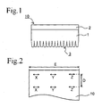
- An acrylic adhesive was then applied to a thickness of 20 ⁇ m, producing adhesive sheets for laser processing 10 with the adhesive layer 2 formed on the surface of the base film 1 and the contact-reducing layer 3 formed on the back side, as shown in Fig 1.
- the surface of the contact-reducing layer was measured for a length of 50 mm in each location.
- the adhesive sheet for laser processing was disposed on a quartz glass table as a chuck table of a laser dicing apparatus using a ling for fixing 11, so as to contact with the side of the contact-reducing layer.
- a third harmonic (355 nm) of a YAG laser with a wavelength of 355 nm as a processing laser, an average output of 5 W, and a repeated frequency of 30 kHz was used.
- the laser light was focused with an f ⁇ lens on the surface of the adhesive sheet for laser processing, and was scanned with a galvano scanner at a rate of 20 mm/second to cut the sheet.
- the adhesion strength was measured by varying the number of scans to between 1 and 8 times.
- the adhesive strength between the adhesive sheet for laser processing and the chuck table was measured according to the JIS Z0237 adhesive strength measurement method. That is, as the test piece, a laser processed adhesive sheet for laser processing 10 was cut to a width A of 20 mm and a length B of 150 mm, and the tension tester stipulated in JIS B7721 was used as the measurement device to measure the load (adhesive strength, N/20 mm) when separated at a measuring temperature of 23 ⁇ 3°C, a release angle of 180°, and a release speed of 300 mm/sec.
- a 150 ⁇ m thick polyethylene film was formed using 2 mirror metal rolls, without any hot machining roll having a machined depth, giving a polyethylene film without a contact-reducing layer.
- Measurement of the arithmetical mean deviation of the surface Ra on both sides of the film revealed a value of 0.4 ⁇ m on both sides, as indicated in Table 1.
- Example 2 An embossing process, formation of the contact-reducing layer, and an evaluation were conducted in the same manner as in Example 1, except that A polypropylene/polyethylene/ polypropylene composite film (film thickness: 30 ⁇ m/90 ⁇ m/30gm, melting point: 130°C, a light transmittance of 70% to 355 nm light) was used as the base film.
- the adhesive sheet for laser processing was cut to some extent during multiple laser scanning times, virtually the same results as above were obtained in terms of the adhesion of the adhesive sheet for laser processing to the chuck table.
Landscapes
- Chemical & Material Sciences (AREA)
- Organic Chemistry (AREA)
- Engineering & Computer Science (AREA)
- Physics & Mathematics (AREA)
- Optics & Photonics (AREA)
- Plasma & Fusion (AREA)
- Mechanical Engineering (AREA)
- Chemical Kinetics & Catalysis (AREA)
- Laser Beam Processing (AREA)
- Dicing (AREA)
- Adhesive Tapes (AREA)
- Adhesives Or Adhesive Processes (AREA)
Applications Claiming Priority (1)
| Application Number | Priority Date | Filing Date | Title |
|---|---|---|---|
| JP2006272862A JP4767144B2 (ja) | 2006-10-04 | 2006-10-04 | レーザ加工用粘着シート |
Publications (1)
| Publication Number | Publication Date |
|---|---|
| EP1908808A1 true EP1908808A1 (fr) | 2008-04-09 |
Family
ID=39052670
Family Applications (1)
| Application Number | Title | Priority Date | Filing Date |
|---|---|---|---|
| EP07018523A Withdrawn EP1908808A1 (fr) | 2006-10-04 | 2007-09-20 | Feuille adhésive pour traitement au laser |
Country Status (6)
| Country | Link |
|---|---|
| US (1) | US20080085397A1 (fr) |
| EP (1) | EP1908808A1 (fr) |
| JP (1) | JP4767144B2 (fr) |
| KR (1) | KR20080031628A (fr) |
| CN (1) | CN101157830B (fr) |
| TW (1) | TWI409315B (fr) |
Cited By (1)
| Publication number | Priority date | Publication date | Assignee | Title |
|---|---|---|---|---|
| DE202012102188U1 (de) | 2012-06-14 | 2013-09-26 | Polifilm Protection Gmbh | Partikelhaltige Klebefolie zum temporären Schutz einer Werkstückoberfläche, insbesondere bei Laserbearbeitung, und Verbund mit einer derartigen Folie |
Families Citing this family (33)
| Publication number | Priority date | Publication date | Assignee | Title |
|---|---|---|---|---|
| JP5193752B2 (ja) * | 2008-08-28 | 2013-05-08 | リンテック株式会社 | レーザーダイシングシートおよび半導体チップの製造方法 |
| JP5537789B2 (ja) * | 2008-10-01 | 2014-07-02 | 日東電工株式会社 | レーザー加工用粘着シート及びレーザー加工方法 |
| CN102460655B (zh) * | 2009-06-15 | 2015-05-13 | Lg化学株式会社 | 晶片处理薄片 |
| JP2011198914A (ja) * | 2010-03-18 | 2011-10-06 | Lintec Corp | 半導体用接着剤組成物、半導体用接着シートおよび半導体装置の製造方法 |
| EP2650912B1 (fr) * | 2010-12-06 | 2015-06-24 | Kimoto Co., Ltd. | Couche auxiliaire pour découpe au laser |
| JP2013021105A (ja) * | 2011-07-11 | 2013-01-31 | Nitto Denko Corp | ダイシング用粘着シート、及び、ダイシング用粘着シートを用いた半導体装置の製造方法 |
| KR101924484B1 (ko) * | 2011-10-17 | 2018-12-04 | 닛토덴코 가부시키가이샤 | 점착 테이프용 필름 및 점착 테이프 |
| KR101920086B1 (ko) * | 2011-10-17 | 2018-11-19 | 닛토덴코 가부시키가이샤 | 점착 테이프용 필름 및 점착 테이프 |
| JP5978051B2 (ja) * | 2011-10-17 | 2016-08-24 | 日東電工株式会社 | 粘着テープ用フィルムおよび粘着テープ |
| JP5019657B1 (ja) * | 2011-10-27 | 2012-09-05 | 古河電気工業株式会社 | 半導体デバイス加工用粘着テープ |
| JP6005952B2 (ja) * | 2012-02-28 | 2016-10-12 | 日東電工株式会社 | 粘着テープ用フィルムおよび粘着テープ |
| JP5946289B2 (ja) * | 2012-02-28 | 2016-07-06 | 日東電工株式会社 | 粘着テープ用フィルムおよび粘着テープ |
| JP6110662B2 (ja) * | 2012-12-28 | 2017-04-05 | リンテック株式会社 | ダイシングシート用基材フィルムおよびダイシングシート |
| JP6029481B2 (ja) * | 2013-02-04 | 2016-11-24 | リンテック株式会社 | レーザーダイシングシートおよび半導体チップの製造方法 |
| JP6211771B2 (ja) * | 2013-02-08 | 2017-10-11 | 日東電工株式会社 | 粘着テープ |
| JP6303281B2 (ja) * | 2013-04-08 | 2018-04-04 | 大日本印刷株式会社 | 保護テープ、保護テープの製造方法、ダイシングテープ及びダイシングテープの製造方法 |
| US20150037915A1 (en) * | 2013-07-31 | 2015-02-05 | Wei-Sheng Lei | Method and system for laser focus plane determination in a laser scribing process |
| WO2015072259A1 (fr) * | 2013-11-14 | 2015-05-21 | 三菱電機株式会社 | Procédé de traitement au laser et appareil de traitement au laser |
| WO2015190230A1 (fr) * | 2014-06-10 | 2015-12-17 | リンテック株式会社 | Feuille de découpage en dés |
| JP6401043B2 (ja) * | 2014-12-24 | 2018-10-03 | 株式会社きもと | レーザーダイシング用補助シート |
| JP6459646B2 (ja) * | 2015-03-06 | 2019-01-30 | 富士通株式会社 | 半導体装置製造用治具及び半導体装置の製造方法 |
| KR101676025B1 (ko) * | 2016-06-30 | 2016-11-15 | (주) 화인테크놀리지 | 반도체 웨이퍼의 하프커팅 후 이면 연삭 가공용 자외선 경화형 점착시트 |
| JP6286014B2 (ja) * | 2016-12-19 | 2018-02-28 | パナック株式会社 | 工程用保護フィルム |
| JP6795811B2 (ja) * | 2017-02-16 | 2020-12-02 | 国立大学法人埼玉大学 | 剥離基板製造方法 |
| EP3626792B1 (fr) * | 2017-07-20 | 2025-04-30 | Mitsui Chemicals, Inc. | Élément adhésif et procédé de production d'un élément adhésif |
| JP6562095B2 (ja) * | 2018-01-26 | 2019-08-21 | 王子ホールディングス株式会社 | レーザ加工用補助シート |
| CN108389826A (zh) * | 2018-02-11 | 2018-08-10 | 安徽三安光电有限公司 | 用于晶粒扩膜的薄膜及其制作方法 |
| CN109321151A (zh) * | 2018-08-30 | 2019-02-12 | 宁波吉象塑胶科技股份有限公司 | 静音胶带 |
| WO2020047073A1 (fr) | 2018-08-31 | 2020-03-05 | Kimberly-Clark Worldwide, Inc. | Procédés et systèmes de découpe ou de perforation d'une bande à l'aide d'un laser |
| JP7311312B2 (ja) * | 2019-05-17 | 2023-07-19 | 東レフィルム加工株式会社 | ダイシングシート用基材フィルム |
| JP7727370B2 (ja) * | 2019-12-26 | 2025-08-21 | 東洋紡株式会社 | ポリオレフィン系樹脂フィルム、これを用いた粘着シート |
| DE102021124738A1 (de) * | 2021-09-24 | 2023-03-30 | Infineon Technologies Ag | Wafer-chuck für eine laserstrahl-waferzerteilanlage |
| WO2026053642A1 (fr) * | 2024-09-04 | 2026-03-12 | 日東電工株式会社 | Feuille adhésive pour traitement laser |
Citations (9)
| Publication number | Priority date | Publication date | Assignee | Title |
|---|---|---|---|---|
| JP2001011207A (ja) | 1999-07-02 | 2001-01-16 | Gunze Ltd | ポリオレフィン系フィルム |
| JP2001232683A (ja) | 2000-02-23 | 2001-08-28 | Gunze Ltd | 均一拡張性と滑性に優れるポリオレフィン系フィルム |
| JP2002343747A (ja) | 2001-05-17 | 2002-11-29 | Lintec Corp | ダイシングシート及びダイシング方法 |
| JP2003210049A (ja) | 2002-01-23 | 2003-07-29 | Sumitomo Chem Co Ltd | 農業用ハウス被覆材 |
| JP2004079746A (ja) | 2002-08-16 | 2004-03-11 | Tokyo Seimitsu Co Ltd | チップ製造方法 |
| EP1566236A1 (fr) * | 2004-02-20 | 2005-08-24 | Nitto Denko Corporation | Feuille d'adhésif pour découpe laser avec une rugosité arithmétique (ra) controllée et sa méthode de fabrication |
| US20050191456A1 (en) | 2004-02-26 | 2005-09-01 | Kouichi Hashimoto | Adhesive sheet roll for wafer processing |
| JP2006104417A (ja) | 2004-10-08 | 2006-04-20 | Hitachi Chem Co Ltd | 硬化性樹脂組成物、これを用いた硬化性シート及び放熱シート |
| JP2006245487A (ja) | 2005-03-07 | 2006-09-14 | Lintec Corp | レーザーダイシングシートおよびレーザーダイシング方法 |
Family Cites Families (8)
| Publication number | Priority date | Publication date | Assignee | Title |
|---|---|---|---|---|
| JPH10337823A (ja) * | 1997-04-11 | 1998-12-22 | Lintec Corp | 基材および該基材を用いた粘着テープ |
| US7141300B2 (en) * | 2001-06-27 | 2006-11-28 | Nitto Denko Corporation | Adhesive sheet for dicing |
| JP3953801B2 (ja) * | 2001-12-11 | 2007-08-08 | 大日本印刷株式会社 | 拡散フィルム及びその製造方法、面光源装置及び液晶表示装置 |
| WO2004096483A1 (fr) * | 2003-04-25 | 2004-11-11 | Nitto Denko Corporation | Methode de production d'un produit traite par laser et d'une feuille adhesive, pour un traitement laser utilise pour ce produit |
| JP4477346B2 (ja) * | 2003-12-05 | 2010-06-09 | 古河電気工業株式会社 | 半導体ダイシング用粘接着テープ |
| JP4642436B2 (ja) * | 2004-11-12 | 2011-03-02 | リンテック株式会社 | マーキング方法および保護膜形成兼ダイシング用シート |
| JP4712468B2 (ja) * | 2004-11-30 | 2011-06-29 | 古河電気工業株式会社 | ダイシングダイボンドテープ |
| JP4762671B2 (ja) * | 2005-10-26 | 2011-08-31 | 古河電気工業株式会社 | ダイシングテープ、および半導体ウェハダイシング方法 |
-
2006
- 2006-10-04 JP JP2006272862A patent/JP4767144B2/ja not_active Expired - Fee Related
-
2007
- 2007-09-20 EP EP07018523A patent/EP1908808A1/fr not_active Withdrawn
- 2007-09-28 CN CN2007101531718A patent/CN101157830B/zh not_active Expired - Fee Related
- 2007-10-02 KR KR1020070099000A patent/KR20080031628A/ko not_active Ceased
- 2007-10-02 US US11/905,567 patent/US20080085397A1/en not_active Abandoned
- 2007-10-04 TW TW096137333A patent/TWI409315B/zh not_active IP Right Cessation
Patent Citations (10)
| Publication number | Priority date | Publication date | Assignee | Title |
|---|---|---|---|---|
| JP2001011207A (ja) | 1999-07-02 | 2001-01-16 | Gunze Ltd | ポリオレフィン系フィルム |
| JP2001232683A (ja) | 2000-02-23 | 2001-08-28 | Gunze Ltd | 均一拡張性と滑性に優れるポリオレフィン系フィルム |
| JP2002343747A (ja) | 2001-05-17 | 2002-11-29 | Lintec Corp | ダイシングシート及びダイシング方法 |
| JP2003210049A (ja) | 2002-01-23 | 2003-07-29 | Sumitomo Chem Co Ltd | 農業用ハウス被覆材 |
| JP2004079746A (ja) | 2002-08-16 | 2004-03-11 | Tokyo Seimitsu Co Ltd | チップ製造方法 |
| EP1566236A1 (fr) * | 2004-02-20 | 2005-08-24 | Nitto Denko Corporation | Feuille d'adhésif pour découpe laser avec une rugosité arithmétique (ra) controllée et sa méthode de fabrication |
| US20050191456A1 (en) | 2004-02-26 | 2005-09-01 | Kouichi Hashimoto | Adhesive sheet roll for wafer processing |
| JP2005239889A (ja) | 2004-02-26 | 2005-09-08 | Nitto Denko Corp | ロール状ウエハ加工用粘着シート |
| JP2006104417A (ja) | 2004-10-08 | 2006-04-20 | Hitachi Chem Co Ltd | 硬化性樹脂組成物、これを用いた硬化性シート及び放熱シート |
| JP2006245487A (ja) | 2005-03-07 | 2006-09-14 | Lintec Corp | レーザーダイシングシートおよびレーザーダイシング方法 |
Non-Patent Citations (1)
| Title |
|---|
| DATABASE WPI Week 200308, Derwent World Patents Index; AN 2003-086468, XP002470110 * |
Cited By (2)
| Publication number | Priority date | Publication date | Assignee | Title |
|---|---|---|---|---|
| DE202012102188U1 (de) | 2012-06-14 | 2013-09-26 | Polifilm Protection Gmbh | Partikelhaltige Klebefolie zum temporären Schutz einer Werkstückoberfläche, insbesondere bei Laserbearbeitung, und Verbund mit einer derartigen Folie |
| WO2013186041A1 (fr) | 2012-06-14 | 2013-12-19 | Polifilm Protection Gmbh | Feuille adhésive contenant des particules pour la protection temporaire d'une surface d'une pièce à usiner, notamment pour un usinage au laser, et composite comprenant une telle feuille |
Also Published As
| Publication number | Publication date |
|---|---|
| JP2008091765A (ja) | 2008-04-17 |
| JP4767144B2 (ja) | 2011-09-07 |
| TW200833807A (en) | 2008-08-16 |
| KR20080031628A (ko) | 2008-04-10 |
| CN101157830A (zh) | 2008-04-09 |
| US20080085397A1 (en) | 2008-04-10 |
| TWI409315B (zh) | 2013-09-21 |
| CN101157830B (zh) | 2013-08-07 |
Similar Documents
| Publication | Publication Date | Title |
|---|---|---|
| EP1908808A1 (fr) | Feuille adhésive pour traitement au laser | |
| EP1892275A2 (fr) | Feuille adhésive pour traitement au laser | |
| US8168514B2 (en) | Laser separation of thin laminated glass substrates for flexible display applications | |
| US8168030B2 (en) | Manufacturing method of laser processed parts and adhesive sheet for laser processing | |
| JP6733544B2 (ja) | シランカップリング剤層積層ポリイミドフィルム | |
| EP1139415B1 (fr) | Bande adhésive perméable à l'eau pour le traitement de semiconducteurs | |
| JP6447135B2 (ja) | 積層体、積層体の製造方法、およびフレキシブル電子デバイスの製造方法 | |
| US20140041800A1 (en) | Laminate, method for producing same, and method for producing device structure using same | |
| JP2002343747A (ja) | ダイシングシート及びダイシング方法 | |
| JP6401043B2 (ja) | レーザーダイシング用補助シート | |
| WO2004096483A1 (fr) | Methode de production d'un produit traite par laser et d'une feuille adhesive, pour un traitement laser utilise pour ce produit | |
| TW202033374A (zh) | 疊層薄膜、疊層體、及疊層體之製造方法 | |
| CN101177598A (zh) | 喷水激光切割用粘合片 | |
| US20160251251A1 (en) | Laser processing method and laser processing apparatus | |
| CN106799548A (zh) | 保护膜、激光切割的方法 | |
| JP2011061097A (ja) | ダイシング用プロセステープ。 | |
| JP4873843B2 (ja) | レーザー加工品の製造方法 | |
| KR102362435B1 (ko) | 레이저 다이싱용 보조 시트 | |
| JP2021175583A (ja) | レーザー加工品の製造方法 | |
| JP2018060994A (ja) | レーザーダイシング用補助シート | |
| EP4574424A1 (fr) | Bande de découpage en dés et procédés associés | |
| WO2004060033A1 (fr) | Produit multicouche pour fabriquer des cartes de circuits imprimes | |
| JP2004338285A (ja) | 粘着テープ用基材および粘着シート |
Legal Events
| Date | Code | Title | Description |
|---|---|---|---|
| PUAI | Public reference made under article 153(3) epc to a published international application that has entered the european phase |
Free format text: ORIGINAL CODE: 0009012 |
|
| AK | Designated contracting states |
Kind code of ref document: A1 Designated state(s): AT BE BG CH CY CZ DE DK EE ES FI FR GB GR HU IE IS IT LI LT LU LV MC MT NL PL PT RO SE SI SK TR |
|
| AX | Request for extension of the european patent |
Extension state: AL BA HR MK RS |
|
| 17P | Request for examination filed |
Effective date: 20080624 |
|
| 17Q | First examination report despatched |
Effective date: 20080729 |
|
| AKX | Designation fees paid |
Designated state(s): BE DE FR GB IT NL |
|
| TPAC | Observations filed by third parties |
Free format text: ORIGINAL CODE: EPIDOSNTIPA |
|
| STAA | Information on the status of an ep patent application or granted ep patent |
Free format text: STATUS: THE APPLICATION IS DEEMED TO BE WITHDRAWN |
|
| 18D | Application deemed to be withdrawn |
Effective date: 20150331 |