EP1904264B1 - Wire bonding capillary apparatus and method - Google Patents
Wire bonding capillary apparatus and method Download PDFInfo
- Publication number
- EP1904264B1 EP1904264B1 EP06772731A EP06772731A EP1904264B1 EP 1904264 B1 EP1904264 B1 EP 1904264B1 EP 06772731 A EP06772731 A EP 06772731A EP 06772731 A EP06772731 A EP 06772731A EP 1904264 B1 EP1904264 B1 EP 1904264B1
- Authority
- EP
- European Patent Office
- Prior art keywords
- wire
- bonding
- bond capillary
- cutting
- cutting tool
- Prior art date
- Legal status (The legal status is an assumption and is not a legal conclusion. Google has not performed a legal analysis and makes no representation as to the accuracy of the status listed.)
- Expired - Fee Related
Links
Images


Classifications
-
- B—PERFORMING OPERATIONS; TRANSPORTING
- B23—MACHINE TOOLS; METAL-WORKING NOT OTHERWISE PROVIDED FOR
- B23K—SOLDERING OR UNSOLDERING; WELDING; CLADDING OR PLATING BY SOLDERING OR WELDING; CUTTING BY APPLYING HEAT LOCALLY, e.g. FLAME CUTTING; WORKING BY LASER BEAM
- B23K1/00—Soldering, e.g. brazing, or unsoldering
- B23K1/06—Soldering, e.g. brazing, or unsoldering making use of vibrations, e.g. supersonic vibrations
-
- B—PERFORMING OPERATIONS; TRANSPORTING
- B23—MACHINE TOOLS; METAL-WORKING NOT OTHERWISE PROVIDED FOR
- B23K—SOLDERING OR UNSOLDERING; WELDING; CLADDING OR PLATING BY SOLDERING OR WELDING; CUTTING BY APPLYING HEAT LOCALLY, e.g. FLAME CUTTING; WORKING BY LASER BEAM
- B23K20/00—Non-electric welding by applying impact or other pressure, with or without the application of heat, e.g. cladding or plating
- B23K20/002—Non-electric welding by applying impact or other pressure, with or without the application of heat, e.g. cladding or plating specially adapted for particular articles or work
- B23K20/004—Wire welding
- B23K20/005—Capillary welding
-
- B—PERFORMING OPERATIONS; TRANSPORTING
- B23—MACHINE TOOLS; METAL-WORKING NOT OTHERWISE PROVIDED FOR
- B23K—SOLDERING OR UNSOLDERING; WELDING; CLADDING OR PLATING BY SOLDERING OR WELDING; CUTTING BY APPLYING HEAT LOCALLY, e.g. FLAME CUTTING; WORKING BY LASER BEAM
- B23K20/00—Non-electric welding by applying impact or other pressure, with or without the application of heat, e.g. cladding or plating
- B23K20/002—Non-electric welding by applying impact or other pressure, with or without the application of heat, e.g. cladding or plating specially adapted for particular articles or work
- B23K20/004—Wire welding
-
- B—PERFORMING OPERATIONS; TRANSPORTING
- B23—MACHINE TOOLS; METAL-WORKING NOT OTHERWISE PROVIDED FOR
- B23K—SOLDERING OR UNSOLDERING; WELDING; CLADDING OR PLATING BY SOLDERING OR WELDING; CUTTING BY APPLYING HEAT LOCALLY, e.g. FLAME CUTTING; WORKING BY LASER BEAM
- B23K20/00—Non-electric welding by applying impact or other pressure, with or without the application of heat, e.g. cladding or plating
- B23K20/10—Non-electric welding by applying impact or other pressure, with or without the application of heat, e.g. cladding or plating making use of vibrations, e.g. ultrasonic welding
- B23K20/106—Features related to sonotrodes
-
- B—PERFORMING OPERATIONS; TRANSPORTING
- B23—MACHINE TOOLS; METAL-WORKING NOT OTHERWISE PROVIDED FOR
- B23K—SOLDERING OR UNSOLDERING; WELDING; CLADDING OR PLATING BY SOLDERING OR WELDING; CUTTING BY APPLYING HEAT LOCALLY, e.g. FLAME CUTTING; WORKING BY LASER BEAM
- B23K37/00—Auxiliary devices or processes, not specially adapted to a procedure covered by only one of the preceding main groups
-
- H—ELECTRICITY
- H01—ELECTRIC ELEMENTS
- H01L—SEMICONDUCTOR DEVICES NOT COVERED BY CLASS H10
- H01L24/00—Arrangements for connecting or disconnecting semiconductor or solid-state bodies; Methods or apparatus related thereto
- H01L24/74—Apparatus for manufacturing arrangements for connecting or disconnecting semiconductor or solid-state bodies
- H01L24/78—Apparatus for connecting with wire connectors
-
- H—ELECTRICITY
- H01—ELECTRIC ELEMENTS
- H01L—SEMICONDUCTOR DEVICES NOT COVERED BY CLASS H10
- H01L24/00—Arrangements for connecting or disconnecting semiconductor or solid-state bodies; Methods or apparatus related thereto
- H01L24/80—Methods for connecting semiconductor or other solid state bodies using means for bonding being attached to, or being formed on, the surface to be connected
- H01L24/85—Methods for connecting semiconductor or other solid state bodies using means for bonding being attached to, or being formed on, the surface to be connected using a wire connector
-
- H—ELECTRICITY
- H01—ELECTRIC ELEMENTS
- H01L—SEMICONDUCTOR DEVICES NOT COVERED BY CLASS H10
- H01L2224/00—Indexing scheme for arrangements for connecting or disconnecting semiconductor or solid-state bodies and methods related thereto as covered by H01L24/00
- H01L2224/01—Means for bonding being attached to, or being formed on, the surface to be connected, e.g. chip-to-package, die-attach, "first-level" interconnects; Manufacturing methods related thereto
- H01L2224/42—Wire connectors; Manufacturing methods related thereto
- H01L2224/44—Structure, shape, material or disposition of the wire connectors prior to the connecting process
- H01L2224/45—Structure, shape, material or disposition of the wire connectors prior to the connecting process of an individual wire connector
- H01L2224/45001—Core members of the connector
- H01L2224/4501—Shape
- H01L2224/45012—Cross-sectional shape
- H01L2224/45014—Ribbon connectors, e.g. rectangular cross-section
-
- H—ELECTRICITY
- H01—ELECTRIC ELEMENTS
- H01L—SEMICONDUCTOR DEVICES NOT COVERED BY CLASS H10
- H01L2224/00—Indexing scheme for arrangements for connecting or disconnecting semiconductor or solid-state bodies and methods related thereto as covered by H01L24/00
- H01L2224/01—Means for bonding being attached to, or being formed on, the surface to be connected, e.g. chip-to-package, die-attach, "first-level" interconnects; Manufacturing methods related thereto
- H01L2224/42—Wire connectors; Manufacturing methods related thereto
- H01L2224/44—Structure, shape, material or disposition of the wire connectors prior to the connecting process
- H01L2224/45—Structure, shape, material or disposition of the wire connectors prior to the connecting process of an individual wire connector
- H01L2224/45001—Core members of the connector
- H01L2224/4501—Shape
- H01L2224/45012—Cross-sectional shape
- H01L2224/45015—Cross-sectional shape being circular
-
- H—ELECTRICITY
- H01—ELECTRIC ELEMENTS
- H01L—SEMICONDUCTOR DEVICES NOT COVERED BY CLASS H10
- H01L2224/00—Indexing scheme for arrangements for connecting or disconnecting semiconductor or solid-state bodies and methods related thereto as covered by H01L24/00
- H01L2224/01—Means for bonding being attached to, or being formed on, the surface to be connected, e.g. chip-to-package, die-attach, "first-level" interconnects; Manufacturing methods related thereto
- H01L2224/42—Wire connectors; Manufacturing methods related thereto
- H01L2224/44—Structure, shape, material or disposition of the wire connectors prior to the connecting process
- H01L2224/45—Structure, shape, material or disposition of the wire connectors prior to the connecting process of an individual wire connector
- H01L2224/45001—Core members of the connector
- H01L2224/45099—Material
- H01L2224/451—Material with a principal constituent of the material being a metal or a metalloid, e.g. boron (B), silicon (Si), germanium (Ge), arsenic (As), antimony (Sb), tellurium (Te) and polonium (Po), and alloys thereof
- H01L2224/45117—Material with a principal constituent of the material being a metal or a metalloid, e.g. boron (B), silicon (Si), germanium (Ge), arsenic (As), antimony (Sb), tellurium (Te) and polonium (Po), and alloys thereof the principal constituent melting at a temperature of greater than or equal to 400°C and less than 950°C
- H01L2224/45124—Aluminium (Al) as principal constituent
-
- H—ELECTRICITY
- H01—ELECTRIC ELEMENTS
- H01L—SEMICONDUCTOR DEVICES NOT COVERED BY CLASS H10
- H01L2224/00—Indexing scheme for arrangements for connecting or disconnecting semiconductor or solid-state bodies and methods related thereto as covered by H01L24/00
- H01L2224/01—Means for bonding being attached to, or being formed on, the surface to be connected, e.g. chip-to-package, die-attach, "first-level" interconnects; Manufacturing methods related thereto
- H01L2224/42—Wire connectors; Manufacturing methods related thereto
- H01L2224/44—Structure, shape, material or disposition of the wire connectors prior to the connecting process
- H01L2224/45—Structure, shape, material or disposition of the wire connectors prior to the connecting process of an individual wire connector
- H01L2224/45001—Core members of the connector
- H01L2224/45099—Material
- H01L2224/451—Material with a principal constituent of the material being a metal or a metalloid, e.g. boron (B), silicon (Si), germanium (Ge), arsenic (As), antimony (Sb), tellurium (Te) and polonium (Po), and alloys thereof
- H01L2224/45138—Material with a principal constituent of the material being a metal or a metalloid, e.g. boron (B), silicon (Si), germanium (Ge), arsenic (As), antimony (Sb), tellurium (Te) and polonium (Po), and alloys thereof the principal constituent melting at a temperature of greater than or equal to 950°C and less than 1550°C
- H01L2224/45144—Gold (Au) as principal constituent
-
- H—ELECTRICITY
- H01—ELECTRIC ELEMENTS
- H01L—SEMICONDUCTOR DEVICES NOT COVERED BY CLASS H10
- H01L2224/00—Indexing scheme for arrangements for connecting or disconnecting semiconductor or solid-state bodies and methods related thereto as covered by H01L24/00
- H01L2224/01—Means for bonding being attached to, or being formed on, the surface to be connected, e.g. chip-to-package, die-attach, "first-level" interconnects; Manufacturing methods related thereto
- H01L2224/42—Wire connectors; Manufacturing methods related thereto
- H01L2224/47—Structure, shape, material or disposition of the wire connectors after the connecting process
- H01L2224/48—Structure, shape, material or disposition of the wire connectors after the connecting process of an individual wire connector
- H01L2224/484—Connecting portions
- H01L2224/4847—Connecting portions the connecting portion on the bonding area of the semiconductor or solid-state body being a wedge bond
-
- H—ELECTRICITY
- H01—ELECTRIC ELEMENTS
- H01L—SEMICONDUCTOR DEVICES NOT COVERED BY CLASS H10
- H01L2224/00—Indexing scheme for arrangements for connecting or disconnecting semiconductor or solid-state bodies and methods related thereto as covered by H01L24/00
- H01L2224/74—Apparatus for manufacturing arrangements for connecting or disconnecting semiconductor or solid-state bodies and for methods related thereto
- H01L2224/78—Apparatus for connecting with wire connectors
- H01L2224/7825—Means for applying energy, e.g. heating means
- H01L2224/783—Means for applying energy, e.g. heating means by means of pressure
- H01L2224/78313—Wedge
- H01L2224/78314—Shape
- H01L2224/78317—Shape of other portions
- H01L2224/78318—Shape of other portions inside the capillary
-
- H—ELECTRICITY
- H01—ELECTRIC ELEMENTS
- H01L—SEMICONDUCTOR DEVICES NOT COVERED BY CLASS H10
- H01L2224/00—Indexing scheme for arrangements for connecting or disconnecting semiconductor or solid-state bodies and methods related thereto as covered by H01L24/00
- H01L2224/80—Methods for connecting semiconductor or other solid state bodies using means for bonding being attached to, or being formed on, the surface to be connected
- H01L2224/85—Methods for connecting semiconductor or other solid state bodies using means for bonding being attached to, or being formed on, the surface to be connected using a wire connector
- H01L2224/852—Applying energy for connecting
- H01L2224/85201—Compression bonding
- H01L2224/85205—Ultrasonic bonding
-
- H—ELECTRICITY
- H01—ELECTRIC ELEMENTS
- H01L—SEMICONDUCTOR DEVICES NOT COVERED BY CLASS H10
- H01L24/00—Arrangements for connecting or disconnecting semiconductor or solid-state bodies; Methods or apparatus related thereto
- H01L24/01—Means for bonding being attached to, or being formed on, the surface to be connected, e.g. chip-to-package, die-attach, "first-level" interconnects; Manufacturing methods related thereto
- H01L24/42—Wire connectors; Manufacturing methods related thereto
- H01L24/44—Structure, shape, material or disposition of the wire connectors prior to the connecting process
- H01L24/45—Structure, shape, material or disposition of the wire connectors prior to the connecting process of an individual wire connector
-
- H—ELECTRICITY
- H01—ELECTRIC ELEMENTS
- H01L—SEMICONDUCTOR DEVICES NOT COVERED BY CLASS H10
- H01L24/00—Arrangements for connecting or disconnecting semiconductor or solid-state bodies; Methods or apparatus related thereto
- H01L24/01—Means for bonding being attached to, or being formed on, the surface to be connected, e.g. chip-to-package, die-attach, "first-level" interconnects; Manufacturing methods related thereto
- H01L24/42—Wire connectors; Manufacturing methods related thereto
- H01L24/47—Structure, shape, material or disposition of the wire connectors after the connecting process
- H01L24/48—Structure, shape, material or disposition of the wire connectors after the connecting process of an individual wire connector
-
- H—ELECTRICITY
- H01—ELECTRIC ELEMENTS
- H01L—SEMICONDUCTOR DEVICES NOT COVERED BY CLASS H10
- H01L2924/00—Indexing scheme for arrangements or methods for connecting or disconnecting semiconductor or solid-state bodies as covered by H01L24/00
- H01L2924/0001—Technical content checked by a classifier
- H01L2924/00014—Technical content checked by a classifier the subject-matter covered by the group, the symbol of which is combined with the symbol of this group, being disclosed without further technical details
-
- H—ELECTRICITY
- H01—ELECTRIC ELEMENTS
- H01L—SEMICONDUCTOR DEVICES NOT COVERED BY CLASS H10
- H01L2924/00—Indexing scheme for arrangements or methods for connecting or disconnecting semiconductor or solid-state bodies as covered by H01L24/00
- H01L2924/01—Chemical elements
- H01L2924/01006—Carbon [C]
-
- H—ELECTRICITY
- H01—ELECTRIC ELEMENTS
- H01L—SEMICONDUCTOR DEVICES NOT COVERED BY CLASS H10
- H01L2924/00—Indexing scheme for arrangements or methods for connecting or disconnecting semiconductor or solid-state bodies as covered by H01L24/00
- H01L2924/01—Chemical elements
- H01L2924/01013—Aluminum [Al]
-
- H—ELECTRICITY
- H01—ELECTRIC ELEMENTS
- H01L—SEMICONDUCTOR DEVICES NOT COVERED BY CLASS H10
- H01L2924/00—Indexing scheme for arrangements or methods for connecting or disconnecting semiconductor or solid-state bodies as covered by H01L24/00
- H01L2924/01—Chemical elements
- H01L2924/01029—Copper [Cu]
-
- H—ELECTRICITY
- H01—ELECTRIC ELEMENTS
- H01L—SEMICONDUCTOR DEVICES NOT COVERED BY CLASS H10
- H01L2924/00—Indexing scheme for arrangements or methods for connecting or disconnecting semiconductor or solid-state bodies as covered by H01L24/00
- H01L2924/01—Chemical elements
- H01L2924/01033—Arsenic [As]
-
- H—ELECTRICITY
- H01—ELECTRIC ELEMENTS
- H01L—SEMICONDUCTOR DEVICES NOT COVERED BY CLASS H10
- H01L2924/00—Indexing scheme for arrangements or methods for connecting or disconnecting semiconductor or solid-state bodies as covered by H01L24/00
- H01L2924/01—Chemical elements
- H01L2924/01079—Gold [Au]
-
- H—ELECTRICITY
- H01—ELECTRIC ELEMENTS
- H01L—SEMICONDUCTOR DEVICES NOT COVERED BY CLASS H10
- H01L2924/00—Indexing scheme for arrangements or methods for connecting or disconnecting semiconductor or solid-state bodies as covered by H01L24/00
- H01L2924/01—Chemical elements
- H01L2924/01082—Lead [Pb]
-
- H—ELECTRICITY
- H01—ELECTRIC ELEMENTS
- H01L—SEMICONDUCTOR DEVICES NOT COVERED BY CLASS H10
- H01L2924/00—Indexing scheme for arrangements or methods for connecting or disconnecting semiconductor or solid-state bodies as covered by H01L24/00
- H01L2924/013—Alloys
- H01L2924/014—Solder alloys
-
- H—ELECTRICITY
- H01—ELECTRIC ELEMENTS
- H01L—SEMICONDUCTOR DEVICES NOT COVERED BY CLASS H10
- H01L2924/00—Indexing scheme for arrangements or methods for connecting or disconnecting semiconductor or solid-state bodies as covered by H01L24/00
- H01L2924/10—Details of semiconductor or other solid state devices to be connected
- H01L2924/11—Device type
- H01L2924/14—Integrated circuits
-
- H—ELECTRICITY
- H01—ELECTRIC ELEMENTS
- H01L—SEMICONDUCTOR DEVICES NOT COVERED BY CLASS H10
- H01L2924/00—Indexing scheme for arrangements or methods for connecting or disconnecting semiconductor or solid-state bodies as covered by H01L24/00
- H01L2924/20—Parameters
- H01L2924/207—Diameter ranges
- H01L2924/2076—Diameter ranges equal to or larger than 100 microns
Definitions
- the invention relates generally to semiconductor devices and processes, and more particularly to an apparatus for and a method of bonding a wire, especially such as a ribbon or large sized wire, to a bond pad, or the like, in connection with the fabrication of a semiconductor device according to the preamble of claims 1 and 6 respectively (see for example US 4 976 392 ).
- wire bonding is commonly performed to electrically interconnect an integrated circuit (IC), such as a semiconductor die or chip, to various structures, such as a metal leadframe.
- Wedge bonding is a conventional method used to bond thin wires, such as thin aluminum or gold wire, between a bonding point on the semiconductor die to another point, such as a lead finger of the leadframe.
- the wire is pressed against the IC and/or leadframe with a tip of a bonding tool.
- the bonding tool is ultrasonically vibrated for a period of tens of milliseconds, wherein a plane of motion of the tip of the bonding tool is generally parallel to the surface of the semiconductor chip to which the bond is to be formed.
- wire bonding One problem associated with wire bonding is the handling of the wire throughout the bonding process, and the breaking or severing of the wire after the bond has been made. To perform these functions, most conventional fine wire wedge bonding tools break the wire by clamping and/or pulling the wire away from the bonded substrate. Typically, with small diameter wires (circular cross-section wires having diameters of less than 0.025 inches), such a pulling action is sufficient, and does not cause significant damage to the substrate.
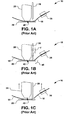
- FIGS. 1A-1C illustrate one such conventional bonding device 10 during various operations, wherein a ribbon wire 15 is bonded to a substrate 20, such as a leadframe finger or semiconductor chip by an ultrasonic bonding tool 25.
- a ribbon wire 15 is bonded to a substrate 20, such as a leadframe finger or semiconductor chip by an ultrasonic bonding tool 25.
- the bonding tool 25 is pressed against the ribbon wire 15, thus compressing the ribbon wire between the bonding tool and the substrate 20.
- the bonding tool 25 ultrasonically vibrates, thus cold-welding the ribbon wire 15 to the substrate 20.
- FIG. 1B illustrates a cutter 30 that is pressed against the ribbon wire 15, wherein the cutter significantly thins or cuts through the ribbon wire by the force F exerted by the cutter.
- FIG. 1C illustrates the bonding tool 25 being pulled away from the substrate 20, wherein a clamp 35 further pulls the ribbon wire 15 from the substrate, thus fully severing the ribbon wire generally at a tip 40 of the cutter 30.
- the force F of the cutter 30 against the ribbon wire 15 illustrated in FIG. 1B typically translates into a force on the substrate 20, wherein the substrate is potentially permanently deforming and/or damaged by the cutting operation.
- the force F significantly deforms the leadframe finger (as illustrated by arrow 45), wherein the deformation remains after the cutter is pulled away from the substrate 20.
- the pulling force may further bend the leadframe finger in a direction opposite of the arrow 45 when the clamp 35 pulls the ribbon wire away.
- the cutting force F can deleteriously impact the chip, such as potentially damaging metallization layers or other layers of the IC.
- United States Patent No. 4976392 describes an ultrasonic wire bonding apparatus having a wire delivery conduit for removing coil set in the wire through a serpentine movement prior to being bonded, which also provides sufficient drag to prevent displacement as the bonder with the wire is being moved from one location to another, and which orients the wire to said bonding tool end.
- An improved wire cutter moves independently of the wire bonding tool and is directly connected to the main Z positioning movement of said wire bonder so that the wire bonding tool and the cutter can move independently during the process.
- the wire bonding tool can be biased by a magnetic bias with an armature connected to the wire bonding tool.
- a loop is provided in the wire between first and second bonds by forming a bend in the wire as it moves away from the first point of bonding. After a second bond, the wire is partially cut by a cutter that moves relative to the bonding tool to partially cut the wire which is then severed by pulling the bonding tool and cleating the wire in the end thereof.
- United Kingdom Patent No. 2177639 describes an ultrasonic bonder for simultaneous bonding of two connecting wires on a contact area of a semiconductor device
- the bonder has a single bonding head having two bonding wedges and grooves for location of wires and two guides through a tongue at the rear of the bonding head.
- the bonding time required for two wires of a given diameter is the same as that required to bond a single wire of the same diameter, thus twin connecting wires may be provided in half the bonding cycle time and the wire spacing is accurately determined without operator intervention.
- United States Patent No. 5452841 describes a wire bonding method comprising welding one end of a ribbon shaped flat copper wire to a terminal and welding the other end of the copper wire to a pad disposed at a level below the level of the terminal, while turning the intermediate portion of the copper wire on and around the cylindrical portion of the forming member which is disposed at a level above the terminal within the horizontal span between the pad and the terminal.
- the wire is bent to form a first acute bend and then bent back to form a second acute bend and is then extended to the pad.
- United States Patent Application No. 2004/188499 describes a wire bonding method including bonding a tip portion of a wire to a first electrode by pressing an open end section of a first hole of a first tool against the tip portion of the wire that is passed through the first hole and protrudes outside the first hole, and bonding a part of a section of the wire that is lead out from the first electrode to a second electrode.
- the first tool is passed through a second hole of a second tool.
- the width of an open end section of the second hole is formed greater than the width of the open end section of the first hole.
- the invention overcomes the limitations of the prior art by providing improved apparatus and methods for bonding wires, especially larger sized or ribbon wires, to various substrates.
- the invention resides in an apparatus for and a method of bonding a wire to a substrate or workpiece as as defined in claims 1 and 6 respectively.
- Penetration of the ribbon wire between the bonding surface and the engagement surface while the ribbon wire is substantially clamped with respect to the bond capillary is highly advantageous over the prior art, since the cutting action of the cutting tool does not press on the workpiece, but rather, cuts the ribbon wire between two generally fixed and/or clamped regions.
- the invention is directed towards an apparatus and method for bonding a wire to a substrate or workpiece, such as an integrated circuit (IC) and/or leadframe assembly. More particularly, the invention provides a robust and reliable device and process for bonding a rectangular cross-section ribbon wire to the substrate, wherein damages or deformations to the substrate seen in conventional bonding apparatuses and processes are substantially mitigated. Accordingly, the invention will now be described with reference to the drawings, wherein like reference numerals are used to refer to like elements throughout.
- FIG. 2 is a cross-sectional view of an example bonding device 100, illustrating the invention.
- the bonding device 100 comprises an ultrasonic bond capillary 102 for ultrasonically bonding a ribbon wire 104 to a substrate or workpiece 106, such as one or more of an IC chip or a leadframe.
- the ultrasonic bond capillary 102 for example, is operably coupled to an ultrasonic oscillator (not shown), as is known in the art for providing an ultrasonic vibration to the bond capillary.
- the ultrasonic bond capillary 102 comprises a body region 108 and a bonding region 110, wherein the ultrasonic bond capillary is operable to sandwich the ribbon wire 104 between a bonding surface 112 of the ultrasonic bond capillary and a surface 114 of the workpiece 106.
- the body region 108 of the bond capillary 102 for example, comprises a passageway 116 defined therein, wherein the ribbon wire 104 further generally extends through the passageway and along the bonding surface 114 associated with the bonding region 110.
- the passageway 116 may be comprised of a thru-hole, a channel, or various other surfaces (not shown) defined within or along the body region 108, wherein the ribbon wire 104 is operable to extend along the passageway.
- the ribbon wire 104 is generally rectangular in cross-section, wherein the passageway is also generally rectangular in cross-section.
- FIG. 2 further illustrates a clamping jaw 118 operably coupled to the bond capillary 102 in the body region 110 thereof, wherein the clamping jaw is further associated with the passageway 116.
- the clamping jaw 118 is operable to selectively grip the ribbon wire 104 between an engagement surface 120 of the passageway 116 of the bond capillary 102 and a clamping surface 122 of the clamping jaw 118.
- the engagement surface 120 of passageway 116 is generally planar, wherein the passageway is generally defined between the body region 110 of the bond capillary 102 and the clamping surface 122 of the clamping jaw 118.
- the passageway 116 may be defined by a channel (not shown) or other structure associated with the body region 110 of the bond capillary 102, wherein the clamping jaw 118 is operable to substantially grip or prevent movement of the ribbon wire 104 within the passageway.
- the clamping jaw 118 of the invention may be operably coupled to an electro-mechanical actuator (not shown), wherein the electro-mechanical actuator is operable to retract and/or extend the clamping jaw, thus respectively gripping and/or releasing the ribbon wire 104.
- the clamping jaw 118 may be operably coupled to a motor (not shown), such as a servo motor, wherein the motor is operable to selectively extend and retract the clamping jaw with respect to the engagement surface 120.
- the clamping jaw 118 may be further coupled to one or more springs (not shown), wherein the one or more springs are further operable to substantially extend or retract the clamping jaw with respect to the engagement surface 120.
- the clamping jaw 118 may be operably coupled to a pneumatic or hydraulic actuator (not shown), wherein the pneumatic or hydraulic actuator is operable to extend and retract the clamping jaw with respect to the engagement surface 120. Accordingly, any actuator operable to extend and/or retract the clamping jaw 118 with respect to the engagement surface 120 of the bond capillary 102 is contemplated as falling within the scope of the invention. It should also be noted that the clamping jaw is generally integrated with the bond capillary 102, wherein the engagement surface 120 of the bond capillary 102 is generally near the bonding surface 114, as will be discussed hereafter.
- the bonding device 100 further comprises a cutting tool 124, wherein the cutting tool is further operably coupled to the bond capillary 102.
- the cutting tool 124 for example, is generally positioned between the bonding surface 114 and the engagement surface 120 of the bond capillary 102, wherein the cutting tool is operable to selectively extend and retract with respect to the bond capillary.
- the cutting tool 124 for example, comprises an elongate member 126, wherein a cutting blade 128 is generally defined at a distal end 130 thereof.
- the cutting blade 128, for example, may be flattened, as illustrated in FIG. 2 , or may alternatively converge to a point (not shown) at the distal end 130 of the cutting tool.
- the cutting tool 124 is operable to penetrate, at least partially, through the ribbon wire 104 between the bonding surface 114 and engagement surface 120 of the ultrasonic bond capillary 102 when the cutting blade 128 is extended past the clamping surface 122 of the clamping jaw 118 in a shear-like manner.
- the cutting tool 124 comprises a ring cutter 132, as illustrated in FIG. 3 .
- the ring cutter 132 for example, comprises a ring 134 positioned at the distal end 130 of the cutting tool 124 of FIG. 2 , wherein the ribbon wire 104 generally passes through an inner region 136 of the ring.
- the ring cutter 132 of FIG. 3 is operable to selectively extend and retract in a manner similar to the cutting blade 128 of FIG. 2 , however, a cutting surface 138 of the ring cutter is operable to generally pass through the ribbon wire when being retracted towards the body region 110 of the bond capillary 102. Accordingly, the ring cutter of FIG. 3 is operable to be drawn against the engagement surface 120 of the bond capillary, thus penetrating, at least partially, through the ribbon wire 104.
- the cutting tool 124 of FIG. 2 is operably coupled to a cutting actuator (not shown), such as an electro-mechanical actuator, servo motor, or other actuator, such as those described in reference to the clamping jaw 118.
- the cutting tool 124 may be coupled to a magnetic actuator (not shown) and a spring (not shown), wherein the magnetic actuator is operable to retract the cutting tool (e.g., pull the distal end 130 of the cutting tool toward the body region 108 of the bond capillary 102), and wherein the spring is operable to provide a return force to the cutting tool, thus extending or returning the distal end of the cutting tool to its original position.
- FIGS. 4 and 5A-5F illustrate steps of a method 200 for bonding a ribbon wire to a substrate applied to the bonding apparatus, in order to understand the implementation of the invention. It will be appreciated that the illustrated order of events may be varied as appropriate to suit particular needs.
- Method 200 begins with act 205, wherein a ribbon wire is fed through a bond capillary. As illustrated in FIG. 5A , the ribbon wire 104 is fed through the passageway 116 of the bond capillary 102 when the clamping jaw 118 is generally extended, thus generally permitting the advancement of the ribbon wire through the passageway.
- act 210 of FIG. 4 the ribbon wire is clamped against the bond capillary, and the result of act 210 is illustrated in FIG. 5B .
- the clamping jaw 118 generally sandwiches the ribbon wire 104 between the clamping surface 122 of the clamping jaw and the engagement surface 120 of the bond capillary 102.
- the ribbon wire is bonded to the workpiece, such as by a cold welding the ribbon wire 104 of FIG. 5B to the workpiece 106 by ultrasonic vibration of the bond capillary 102.
- the ribbon wire can be cut by the cutting tool 124 in act 220 of FIG. 4 .
- FIGS. 5C-5D illustrate the cutting tool 124 extending from the body region 108 of the bond capillary 102, wherein in FIG. 5D , the cutting tool 124 completely severs the ribbon wire 104.
- the ring cutter is retracted toward the bond capillary to cut the ribbon wire 104 of FIGS. 5A-5F .
- the bonding tool 100 can be lifted from the workpiece 106, as illustrated in FIG. 5E , thus providing a secure bond 140 of the ribbon wire to the workpiece without damaging, bending, or otherwise deleteriously affecting the workpiece, as illustrated in FIG. 5F .
- the invention provides apparatus and methods for bonding wire, such as ribbon wire, to a workpiece, wherein the cutting or severing of the wire is performed in a manner that does not significantly deform the workpiece.
- wire such as ribbon wire
- the invention provides a bonding device that can be easily rotated between bonding positions, thus providing an efficient and reliable bonding of a ribbon wire between the bonding positions.
Applications Claiming Priority (2)
| Application Number | Priority Date | Filing Date | Title |
|---|---|---|---|
| US11/148,687 US7216794B2 (en) | 2005-06-09 | 2005-06-09 | Bond capillary design for ribbon wire bonding |
| PCT/US2006/022530 WO2006135773A1 (en) | 2005-06-09 | 2006-06-09 | Wire bonding capillary apparatus and method |
Publications (3)
| Publication Number | Publication Date |
|---|---|
| EP1904264A1 EP1904264A1 (en) | 2008-04-02 |
| EP1904264A4 EP1904264A4 (en) | 2009-05-13 |
| EP1904264B1 true EP1904264B1 (en) | 2011-08-10 |
Family
ID=37523246
Family Applications (1)
| Application Number | Title | Priority Date | Filing Date |
|---|---|---|---|
| EP06772731A Expired - Fee Related EP1904264B1 (en) | 2005-06-09 | 2006-06-09 | Wire bonding capillary apparatus and method |
Country Status (7)
| Country | Link |
|---|---|
| US (2) | US7216794B2 (zh) |
| EP (1) | EP1904264B1 (zh) |
| JP (1) | JP2008543115A (zh) |
| KR (1) | KR20080015925A (zh) |
| CN (1) | CN101171098A (zh) |
| TW (1) | TWI297297B (zh) |
| WO (1) | WO2006135773A1 (zh) |
Families Citing this family (77)
| Publication number | Priority date | Publication date | Assignee | Title |
|---|---|---|---|---|
| US8525314B2 (en) | 2004-11-03 | 2013-09-03 | Tessera, Inc. | Stacked packaging improvements |
| US8058101B2 (en) | 2005-12-23 | 2011-11-15 | Tessera, Inc. | Microelectronic packages and methods therefor |
| US7740176B2 (en) * | 2006-06-09 | 2010-06-22 | Hand Held Products, Inc. | Indicia reading apparatus having reduced trigger-to-read time |
| US7537149B2 (en) * | 2006-09-26 | 2009-05-26 | Orthodyne Electronics Corporation | Deep access large ribbon bond head |
| US20080197461A1 (en) * | 2007-02-15 | 2008-08-21 | Taiwan Semiconductor Manufacturing Co.,Ltd. | Apparatus for wire bonding and integrated circuit chip package |
| US7800207B2 (en) * | 2007-10-17 | 2010-09-21 | Fairchild Semiconductor Corporation | Method for connecting a die attach pad to a lead frame and product thereof |
| US7597235B2 (en) * | 2007-11-15 | 2009-10-06 | Infineon Technologies Ag | Apparatus and method for producing a bonding connection |
| JP2010074499A (ja) * | 2008-09-18 | 2010-04-02 | Panasonic Electric Works Co Ltd | リレー装置 |
| US7762449B2 (en) * | 2008-11-21 | 2010-07-27 | Asm Assembly Automation Ltd | Bond head for heavy wire bonder |
| US8141765B2 (en) * | 2009-01-20 | 2012-03-27 | Orthodyne Electronics Corporation | Cutting blade for a wire bonding system |
| US8129220B2 (en) | 2009-08-24 | 2012-03-06 | Hong Kong Polytechnic University | Method and system for bonding electrical devices using an electrically conductive adhesive |
| JP4791571B2 (ja) * | 2009-11-26 | 2011-10-12 | 田中電子工業株式会社 | 超音波ボンディング用アルミニウムリボン |
| WO2012012335A2 (en) * | 2010-07-19 | 2012-01-26 | Orthodyne Electronics Corporation | Ultrasonic bonding systems including workholder and ribbon feeding system |
| US8482111B2 (en) | 2010-07-19 | 2013-07-09 | Tessera, Inc. | Stackable molded microelectronic packages |
| US9159708B2 (en) | 2010-07-19 | 2015-10-13 | Tessera, Inc. | Stackable molded microelectronic packages with area array unit connectors |
| US20120032354A1 (en) * | 2010-08-06 | 2012-02-09 | National Semiconductor Corporation | Wirebonding method and device enabling high-speed reverse wedge bonding of wire bonds |
| US7918378B1 (en) * | 2010-08-06 | 2011-04-05 | National Semiconductor Corporation | Wire bonding deflector for a wire bonder |
| US8231044B2 (en) | 2010-10-01 | 2012-07-31 | Orthodyne Electronics Corporation | Solar substrate ribbon bonding system |
| US8196798B2 (en) | 2010-10-08 | 2012-06-12 | Kulicke And Soffa Industries, Inc. | Solar substrate ribbon bonding system |
| KR101075241B1 (ko) | 2010-11-15 | 2011-11-01 | 테세라, 인코포레이티드 | 유전체 부재에 단자를 구비하는 마이크로전자 패키지 |
| US20120146206A1 (en) | 2010-12-13 | 2012-06-14 | Tessera Research Llc | Pin attachment |
| KR101128063B1 (ko) | 2011-05-03 | 2012-04-23 | 테세라, 인코포레이티드 | 캡슐화 층의 표면에 와이어 본드를 구비하는 패키지 적층형 어셈블리 |
| US8618659B2 (en) | 2011-05-03 | 2013-12-31 | Tessera, Inc. | Package-on-package assembly with wire bonds to encapsulation surface |
| US8404520B1 (en) | 2011-10-17 | 2013-03-26 | Invensas Corporation | Package-on-package assembly with wire bond vias |
| US8946757B2 (en) | 2012-02-17 | 2015-02-03 | Invensas Corporation | Heat spreading substrate with embedded interconnects |
| US9349706B2 (en) | 2012-02-24 | 2016-05-24 | Invensas Corporation | Method for package-on-package assembly with wire bonds to encapsulation surface |
| US8372741B1 (en) | 2012-02-24 | 2013-02-12 | Invensas Corporation | Method for package-on-package assembly with wire bonds to encapsulation surface |
| US8835228B2 (en) | 2012-05-22 | 2014-09-16 | Invensas Corporation | Substrate-less stackable package with wire-bond interconnect |
| US9391008B2 (en) | 2012-07-31 | 2016-07-12 | Invensas Corporation | Reconstituted wafer-level package DRAM |
| US9502390B2 (en) | 2012-08-03 | 2016-11-22 | Invensas Corporation | BVA interposer |
| US8540136B1 (en) | 2012-09-06 | 2013-09-24 | Taiwan Semiconductor Manufacturing Company, Ltd. | Methods for stud bump formation and apparatus for performing the same |
| US8975738B2 (en) | 2012-11-12 | 2015-03-10 | Invensas Corporation | Structure for microelectronic packaging with terminals on dielectric mass |
| US8878353B2 (en) | 2012-12-20 | 2014-11-04 | Invensas Corporation | Structure for microelectronic packaging with bond elements to encapsulation surface |
| US9136254B2 (en) | 2013-02-01 | 2015-09-15 | Invensas Corporation | Microelectronic package having wire bond vias and stiffening layer |
| US9023691B2 (en) | 2013-07-15 | 2015-05-05 | Invensas Corporation | Microelectronic assemblies with stack terminals coupled by connectors extending through encapsulation |
| US9034696B2 (en) | 2013-07-15 | 2015-05-19 | Invensas Corporation | Microelectronic assemblies having reinforcing collars on connectors extending through encapsulation |
| US8883563B1 (en) | 2013-07-15 | 2014-11-11 | Invensas Corporation | Fabrication of microelectronic assemblies having stack terminals coupled by connectors extending through encapsulation |
| JP2015026772A (ja) * | 2013-07-29 | 2015-02-05 | 三菱電機エンジニアリング株式会社 | 接続導体の接合断裁装置及び接合断裁制御方法 |
| US9167710B2 (en) | 2013-08-07 | 2015-10-20 | Invensas Corporation | Embedded packaging with preformed vias |
| US9685365B2 (en) | 2013-08-08 | 2017-06-20 | Invensas Corporation | Method of forming a wire bond having a free end |
| US20150076714A1 (en) | 2013-09-16 | 2015-03-19 | Invensas Corporation | Microelectronic element with bond elements to encapsulation surface |
| US9087815B2 (en) | 2013-11-12 | 2015-07-21 | Invensas Corporation | Off substrate kinking of bond wire |
| US9082753B2 (en) | 2013-11-12 | 2015-07-14 | Invensas Corporation | Severing bond wire by kinking and twisting |
| US9583456B2 (en) | 2013-11-22 | 2017-02-28 | Invensas Corporation | Multiple bond via arrays of different wire heights on a same substrate |
| US9379074B2 (en) | 2013-11-22 | 2016-06-28 | Invensas Corporation | Die stacks with one or more bond via arrays of wire bond wires and with one or more arrays of bump interconnects |
| US9263394B2 (en) | 2013-11-22 | 2016-02-16 | Invensas Corporation | Multiple bond via arrays of different wire heights on a same substrate |
| US9583411B2 (en) | 2014-01-17 | 2017-02-28 | Invensas Corporation | Fine pitch BVA using reconstituted wafer with area array accessible for testing |
| US9214454B2 (en) | 2014-03-31 | 2015-12-15 | Invensas Corporation | Batch process fabrication of package-on-package microelectronic assemblies |
| US10381326B2 (en) | 2014-05-28 | 2019-08-13 | Invensas Corporation | Structure and method for integrated circuits packaging with increased density |
| US9646917B2 (en) | 2014-05-29 | 2017-05-09 | Invensas Corporation | Low CTE component with wire bond interconnects |
| US9412714B2 (en) | 2014-05-30 | 2016-08-09 | Invensas Corporation | Wire bond support structure and microelectronic package including wire bonds therefrom |
| DE102014013452B4 (de) * | 2014-09-17 | 2016-05-19 | Schunk Sonosystems Gmbh | Vorrichtung zum Verschweißen von stabförmigen Leitern |
| USD771168S1 (en) | 2014-10-31 | 2016-11-08 | Coorstek, Inc. | Wire bonding ceramic capillary |
| JP2016100571A (ja) * | 2014-11-26 | 2016-05-30 | 三菱電機エンジニアリング株式会社 | 接続導体の接合断裁装置及び接合断裁制御方法 |
| US9735084B2 (en) | 2014-12-11 | 2017-08-15 | Invensas Corporation | Bond via array for thermal conductivity |
| USD797172S1 (en) | 2015-02-03 | 2017-09-12 | Coorstek, Inc. | Ceramic bonding tool with textured tip |
| USD797171S1 (en) | 2015-02-03 | 2017-09-12 | Coorstek, Inc. | Ceramic bonding tool with textured tip |
| USD797826S1 (en) | 2015-02-03 | 2017-09-19 | Coorstek, Inc. | Ceramic bonding tool with textured tip |
| US9888579B2 (en) | 2015-03-05 | 2018-02-06 | Invensas Corporation | Pressing of wire bond wire tips to provide bent-over tips |
| USD753739S1 (en) | 2015-04-17 | 2016-04-12 | Coorstek, Inc. | Wire bonding wedge tool |
| US9530749B2 (en) | 2015-04-28 | 2016-12-27 | Invensas Corporation | Coupling of side surface contacts to a circuit platform |
| US9502372B1 (en) | 2015-04-30 | 2016-11-22 | Invensas Corporation | Wafer-level packaging using wire bond wires in place of a redistribution layer |
| US9761554B2 (en) | 2015-05-07 | 2017-09-12 | Invensas Corporation | Ball bonding metal wire bond wires to metal pads |
| US10490528B2 (en) | 2015-10-12 | 2019-11-26 | Invensas Corporation | Embedded wire bond wires |
| US9490222B1 (en) | 2015-10-12 | 2016-11-08 | Invensas Corporation | Wire bond wires for interference shielding |
| US10332854B2 (en) | 2015-10-23 | 2019-06-25 | Invensas Corporation | Anchoring structure of fine pitch bva |
| US10181457B2 (en) | 2015-10-26 | 2019-01-15 | Invensas Corporation | Microelectronic package for wafer-level chip scale packaging with fan-out |
| DE102015222011A1 (de) * | 2015-11-09 | 2017-05-11 | Schunk Sonosystems Gmbh | Verfahren zum Schneiden von Schneidgut |
| US10043779B2 (en) | 2015-11-17 | 2018-08-07 | Invensas Corporation | Packaged microelectronic device for a package-on-package device |
| US9659848B1 (en) | 2015-11-18 | 2017-05-23 | Invensas Corporation | Stiffened wires for offset BVA |
| US9984992B2 (en) | 2015-12-30 | 2018-05-29 | Invensas Corporation | Embedded wire bond wires for vertical integration with separate surface mount and wire bond mounting surfaces |
| US9935075B2 (en) | 2016-07-29 | 2018-04-03 | Invensas Corporation | Wire bonding method and apparatus for electromagnetic interference shielding |
| USD868123S1 (en) | 2016-12-20 | 2019-11-26 | Coorstek, Inc. | Wire bonding wedge tool |
| US10299368B2 (en) | 2016-12-21 | 2019-05-21 | Invensas Corporation | Surface integrated waveguides and circuit structures therefor |
| DE102018221950A1 (de) | 2018-12-17 | 2020-06-18 | BINDER tecsys GmbH | Verfahren zur Herstellung und Positionierung elektrischer Verbinder |
| DE102019126644A1 (de) * | 2019-10-02 | 2021-04-08 | F&S Bondtec Semiconductor GmbH | Bondkopf, Drahtbonder mit einem solchen und Verfahren unter Nutzung eines solchen |
| US20210111146A1 (en) * | 2019-10-10 | 2021-04-15 | Skyworks Solutions, Inc. | Cupd wire bond capillary design |
Family Cites Families (37)
| Publication number | Priority date | Publication date | Assignee | Title |
|---|---|---|---|---|
| US3648354A (en) * | 1969-11-17 | 1972-03-14 | Gen Motors Corp | Tailless bonder for filamentary wire leads |
| US3689983A (en) * | 1970-05-11 | 1972-09-12 | Gen Motors Corp | Method of bonding |
| DE3343738C2 (de) * | 1983-12-02 | 1985-09-26 | Deubzer-Eltec GmbH, 8000 München | Verfahren und Vorrichtung zum Bonden eines dünnen, elektrisch leitenden Drahtes an elektrische Kontaktflächen von elektrischen oder elektronischen Bauteilen |
| GB2177639B (en) * | 1985-07-08 | 1988-12-29 | Philips Electronic Associated | Ultrasonic wire bonder and method of manufacturing a semiconductor device therewith |
| US4645118A (en) * | 1985-08-29 | 1987-02-24 | Biggs Kenneth L | Method and means for threading wire bonding machines |
| US4771930A (en) * | 1986-06-30 | 1988-09-20 | Kulicke And Soffa Industries Inc. | Apparatus for supplying uniform tail lengths |
| DE3912580C2 (de) * | 1989-04-17 | 1997-08-21 | F&K Delvotec Bondtechnik Gmbh | Bondstempel |
| US4976392A (en) | 1989-08-11 | 1990-12-11 | Orthodyne Electronics Corporation | Ultrasonic wire bonder wire formation and cutter system |
| US5148959A (en) | 1991-02-07 | 1992-09-22 | Tribotech | Wedge bonding tool |
| US5616520A (en) | 1992-03-30 | 1997-04-01 | Hitachi, Ltd. | Semiconductor integrated circuit device and fabrication method thereof |
| JPH06252531A (ja) * | 1992-07-31 | 1994-09-09 | Fujitsu Ltd | ワイヤ配線方法及び装置 |
| US5365657A (en) * | 1993-02-01 | 1994-11-22 | Advanced Interconnection Technology | Method and apparatus for cutting wire |
| US5364004A (en) * | 1993-05-10 | 1994-11-15 | Hughes Aircraft Company | Wedge bump bonding apparatus and method |
| US5452838A (en) | 1993-07-13 | 1995-09-26 | F & K Delvotec Bondtechnik Gmbh | Bonding head for an ultrasonic bonding machine |
| JP2783125B2 (ja) * | 1993-07-23 | 1998-08-06 | 株式会社デンソー | ワイヤボンディング方法 |
| ES2170102T3 (es) * | 1993-09-24 | 2002-08-01 | Univ British Columbia | Aminociclohexilesteres y utilizacion de los mismos. |
| US5445306A (en) | 1994-05-31 | 1995-08-29 | Motorola, Inc. | Wedge wire bonding tool tip |
| US5868300A (en) | 1995-06-29 | 1999-02-09 | Orthodyne Electronics Corporation | Articulated wire bonder |
| US5647528A (en) | 1996-02-06 | 1997-07-15 | Micron Technology, Inc. | Bondhead lead clamp apparatus and method |
| US5890644A (en) | 1996-01-26 | 1999-04-06 | Micron Technology, Inc. | Apparatus and method of clamping semiconductor devices using sliding finger supports |
| US5894981A (en) * | 1996-11-27 | 1999-04-20 | Orthodyne Electronics Corporation | Integrated pull tester with an ultrasonic wire bonder |
| US5906706A (en) | 1997-06-12 | 1999-05-25 | F & K Delvotec Bondtechnik Gmbh | Wire guide for a bonding machine |
| US6155474A (en) | 1997-12-16 | 2000-12-05 | Texas Instruments Incorporated | Fine pitch bonding technique |
| JPH11330134A (ja) * | 1998-05-12 | 1999-11-30 | Hitachi Ltd | ワイヤボンディング方法およびその装置並びに半導体装置 |
| US6158647A (en) | 1998-09-29 | 2000-12-12 | Micron Technology, Inc. | Concave face wire bond capillary |
| JP3403661B2 (ja) | 1999-02-16 | 2003-05-06 | 宮城沖電気株式会社 | ワイヤボンダ |
| US6276588B1 (en) * | 1999-04-20 | 2001-08-21 | International Rectifier Corp. | Insert-type cutting blade for ultrasonic bonding wire termination |
| US6439448B1 (en) | 1999-11-05 | 2002-08-27 | Orthodyne Electronics Corporation | Large wire bonder head |
| EP1139413B1 (en) | 2000-03-24 | 2005-03-16 | Texas Instruments Incorporated | Wire bonding process |
| JP2002064118A (ja) | 2000-08-22 | 2002-02-28 | Shinkawa Ltd | ワイヤボンディング装置 |
| JP2003163234A (ja) | 2001-11-27 | 2003-06-06 | Nec Electronics Corp | ワイヤボンディング装置およびワイヤボンディング方法 |
| US6667625B1 (en) * | 2001-12-31 | 2003-12-23 | Charles F. Miller | Method and apparatus for detecting wire in an ultrasonic bonding tool |
| EP1352701B1 (de) * | 2002-04-12 | 2007-12-12 | F & K Delvotek Bondtechnik | Bonddraht-Schneidvorrichtung |
| DE60327258D1 (de) * | 2002-12-18 | 2009-05-28 | Nxp Bv | Drahtbondierungserfahren und vorrichtung |
| JP2004221257A (ja) * | 2003-01-14 | 2004-08-05 | Seiko Epson Corp | ワイヤボンディング方法及びワイヤボンディング装置 |
| US7407079B2 (en) * | 2003-10-23 | 2008-08-05 | Orthodyne Electronics Corporation | Automated filament attachment system for vacuum fluorescent display |
| WO2005043266A2 (en) * | 2003-10-31 | 2005-05-12 | Massachusetts Institute Of Technology | Variable reluctance fast positioning system and methods |
-
2005
- 2005-06-09 US US11/148,687 patent/US7216794B2/en active Active
-
2006
- 2006-06-09 TW TW095120645A patent/TWI297297B/zh active
- 2006-06-09 WO PCT/US2006/022530 patent/WO2006135773A1/en active Application Filing
- 2006-06-09 EP EP06772731A patent/EP1904264B1/en not_active Expired - Fee Related
- 2006-06-09 JP JP2008515980A patent/JP2008543115A/ja not_active Abandoned
- 2006-06-09 CN CNA2006800155843A patent/CN101171098A/zh active Pending
- 2006-06-09 KR KR1020087000459A patent/KR20080015925A/ko not_active Application Discontinuation
-
2007
- 2007-04-11 US US11/733,870 patent/US7578422B2/en active Active
Also Published As
| Publication number | Publication date |
|---|---|
| TW200711780A (en) | 2007-04-01 |
| JP2008543115A (ja) | 2008-11-27 |
| CN101171098A (zh) | 2008-04-30 |
| WO2006135773A1 (en) | 2006-12-21 |
| EP1904264A1 (en) | 2008-04-02 |
| TWI297297B (en) | 2008-06-01 |
| US7578422B2 (en) | 2009-08-25 |
| US20070181652A1 (en) | 2007-08-09 |
| US7216794B2 (en) | 2007-05-15 |
| US20060278682A1 (en) | 2006-12-14 |
| EP1904264A4 (en) | 2009-05-13 |
| KR20080015925A (ko) | 2008-02-20 |
Similar Documents
| Publication | Publication Date | Title |
|---|---|---|
| EP1904264B1 (en) | Wire bonding capillary apparatus and method | |
| US6687988B1 (en) | Method for forming pin-form wires and the like | |
| US7808116B2 (en) | Semiconductor device and wire bonding method | |
| US3648354A (en) | Tailless bonder for filamentary wire leads | |
| US5216803A (en) | Method and apparatus for removing bonded connections | |
| TWI557821B (zh) | 半導體裝置的製造方法以及打線裝置 | |
| US20050191839A1 (en) | Multiple-ball wire bonds | |
| KR101867921B1 (ko) | 반도체 장치의 제조 방법, 반도체 장치 및 와이어 본딩 장치 | |
| US4993618A (en) | Wire bonding method | |
| EP0399838B1 (en) | Wire bonding apparatus and method | |
| TWI543284B (zh) | 半導體裝置的製造方法以及打線裝置 | |
| JP7161252B2 (ja) | 半導体装置、半導体装置の製造方法及びワイヤボンディング装置 | |
| US20220020717A1 (en) | Strengthened wire-bond | |
| TWI824354B (zh) | 打線接合裝置、打線切斷方法以及程式 | |
| JPH1041332A (ja) | ワイヤボンダ | |
| CN114207790A (zh) | 打线接合装置及半导体装置的制造方法 | |
| JPH04251948A (ja) | 半導体装置の製造方法 | |
| JPH113964A (ja) | リードフレーム用条材及びその製造方法 | |
| JPH11307575A (ja) | ワイヤボンディング方法 | |
| WO1998032168A1 (en) | Method for doping metallic connecting wire | |
| JPH10229101A (ja) | 超音波ワイヤボンディングツール | |
| JPH054814B2 (zh) |
Legal Events
| Date | Code | Title | Description |
|---|---|---|---|
| PUAI | Public reference made under article 153(3) epc to a published international application that has entered the european phase |
Free format text: ORIGINAL CODE: 0009012 |
|
| 17P | Request for examination filed |
Effective date: 20080109 |
|
| AK | Designated contracting states |
Kind code of ref document: A1 Designated state(s): DE FR GB |
|
| DAX | Request for extension of the european patent (deleted) | ||
| DAX | Request for extension of the european patent (deleted) | ||
| RBV | Designated contracting states (corrected) |
Designated state(s): DE FR GB |
|
| A4 | Supplementary search report drawn up and despatched |
Effective date: 20090416 |
|
| RIC1 | Information provided on ipc code assigned before grant |
Ipc: B23K 1/06 20060101ALI20090408BHEP Ipc: B23K 20/00 20060101ALI20090408BHEP Ipc: B23K 37/00 20060101AFI20070213BHEP Ipc: B23K 20/10 20060101ALI20090408BHEP |
|
| 17Q | First examination report despatched |
Effective date: 20090619 |
|
| GRAP | Despatch of communication of intention to grant a patent |
Free format text: ORIGINAL CODE: EPIDOSNIGR1 |
|
| GRAS | Grant fee paid |
Free format text: ORIGINAL CODE: EPIDOSNIGR3 |
|
| GRAA | (expected) grant |
Free format text: ORIGINAL CODE: 0009210 |
|
| AK | Designated contracting states |
Kind code of ref document: B1 Designated state(s): DE FR GB |
|
| REG | Reference to a national code |
Ref country code: GB Ref legal event code: FG4D |
|
| REG | Reference to a national code |
Ref country code: DE Ref legal event code: R096 Ref document number: 602006023716 Country of ref document: DE Effective date: 20111013 |
|
| PLBE | No opposition filed within time limit |
Free format text: ORIGINAL CODE: 0009261 |
|
| STAA | Information on the status of an ep patent application or granted ep patent |
Free format text: STATUS: NO OPPOSITION FILED WITHIN TIME LIMIT |
|
| 26N | No opposition filed |
Effective date: 20120511 |
|
| REG | Reference to a national code |
Ref country code: DE Ref legal event code: R097 Ref document number: 602006023716 Country of ref document: DE Effective date: 20120511 |
|
| REG | Reference to a national code |
Ref country code: FR Ref legal event code: PLFP Year of fee payment: 11 |
|
| REG | Reference to a national code |
Ref country code: FR Ref legal event code: PLFP Year of fee payment: 12 |
|
| REG | Reference to a national code |
Ref country code: FR Ref legal event code: PLFP Year of fee payment: 13 |
|
| PGFP | Annual fee paid to national office [announced via postgrant information from national office to epo] |
Ref country code: DE Payment date: 20210519 Year of fee payment: 16 Ref country code: FR Payment date: 20210519 Year of fee payment: 16 |
|
| PGFP | Annual fee paid to national office [announced via postgrant information from national office to epo] |
Ref country code: GB Payment date: 20210519 Year of fee payment: 16 |
|
| REG | Reference to a national code |
Ref country code: DE Ref legal event code: R119 Ref document number: 602006023716 Country of ref document: DE |
|
| GBPC | Gb: european patent ceased through non-payment of renewal fee |
Effective date: 20220609 |
|
| PG25 | Lapsed in a contracting state [announced via postgrant information from national office to epo] |
Ref country code: FR Free format text: LAPSE BECAUSE OF NON-PAYMENT OF DUE FEES Effective date: 20220630 |
|
| PG25 | Lapsed in a contracting state [announced via postgrant information from national office to epo] |
Ref country code: GB Free format text: LAPSE BECAUSE OF NON-PAYMENT OF DUE FEES Effective date: 20220609 Ref country code: DE Free format text: LAPSE BECAUSE OF NON-PAYMENT OF DUE FEES Effective date: 20230103 |