EP1883141B1 - LD ou DEL avec une couche de revêtement superréseau - Google Patents
LD ou DEL avec une couche de revêtement superréseau Download PDFInfo
- Publication number
- EP1883141B1 EP1883141B1 EP07013822.7A EP07013822A EP1883141B1 EP 1883141 B1 EP1883141 B1 EP 1883141B1 EP 07013822 A EP07013822 A EP 07013822A EP 1883141 B1 EP1883141 B1 EP 1883141B1
- Authority
- EP
- European Patent Office
- Prior art keywords
- layers
- function
- superlattice
- layer
- type
- Prior art date
- Legal status (The legal status is an assumption and is not a legal conclusion. Google has not performed a legal analysis and makes no representation as to the accuracy of the status listed.)
- Expired - Fee Related
Links
Images
Classifications
-
- H—ELECTRICITY
- H01—ELECTRIC ELEMENTS
- H01S—DEVICES USING THE PROCESS OF LIGHT AMPLIFICATION BY STIMULATED EMISSION OF RADIATION [LASER] TO AMPLIFY OR GENERATE LIGHT; DEVICES USING STIMULATED EMISSION OF ELECTROMAGNETIC RADIATION IN WAVE RANGES OTHER THAN OPTICAL
- H01S5/00—Semiconductor lasers
- H01S5/30—Structure or shape of the active region; Materials used for the active region
- H01S5/34—Structure or shape of the active region; Materials used for the active region comprising quantum well or superlattice structures, e.g. single quantum well [SQW] lasers, multiple quantum well [MQW] lasers or graded index separate confinement heterostructure [GRINSCH] lasers
- H01S5/343—Structure or shape of the active region; Materials used for the active region comprising quantum well or superlattice structures, e.g. single quantum well [SQW] lasers, multiple quantum well [MQW] lasers or graded index separate confinement heterostructure [GRINSCH] lasers in AIIIBV compounds, e.g. AlGaAs-laser, InP-based laser
- H01S5/34333—Structure or shape of the active region; Materials used for the active region comprising quantum well or superlattice structures, e.g. single quantum well [SQW] lasers, multiple quantum well [MQW] lasers or graded index separate confinement heterostructure [GRINSCH] lasers in AIIIBV compounds, e.g. AlGaAs-laser, InP-based laser with a well layer based on Ga(In)N or Ga(In)P, e.g. blue laser
-
- B—PERFORMING OPERATIONS; TRANSPORTING
- B82—NANOTECHNOLOGY
- B82Y—SPECIFIC USES OR APPLICATIONS OF NANOSTRUCTURES; MEASUREMENT OR ANALYSIS OF NANOSTRUCTURES; MANUFACTURE OR TREATMENT OF NANOSTRUCTURES
- B82Y20/00—Nanooptics, e.g. quantum optics or photonic crystals
-
- H—ELECTRICITY
- H01—ELECTRIC ELEMENTS
- H01L—SEMICONDUCTOR DEVICES NOT COVERED BY CLASS H10
- H01L33/00—Semiconductor devices with at least one potential-jump barrier or surface barrier specially adapted for light emission; Processes or apparatus specially adapted for the manufacture or treatment thereof or of parts thereof; Details thereof
- H01L33/02—Semiconductor devices with at least one potential-jump barrier or surface barrier specially adapted for light emission; Processes or apparatus specially adapted for the manufacture or treatment thereof or of parts thereof; Details thereof characterised by the semiconductor bodies
- H01L33/04—Semiconductor devices with at least one potential-jump barrier or surface barrier specially adapted for light emission; Processes or apparatus specially adapted for the manufacture or treatment thereof or of parts thereof; Details thereof characterised by the semiconductor bodies with a quantum effect structure or superlattice, e.g. tunnel junction
- H01L33/06—Semiconductor devices with at least one potential-jump barrier or surface barrier specially adapted for light emission; Processes or apparatus specially adapted for the manufacture or treatment thereof or of parts thereof; Details thereof characterised by the semiconductor bodies with a quantum effect structure or superlattice, e.g. tunnel junction within the light emitting region, e.g. quantum confinement structure or tunnel barrier
-
- H—ELECTRICITY
- H01—ELECTRIC ELEMENTS
- H01L—SEMICONDUCTOR DEVICES NOT COVERED BY CLASS H10
- H01L33/00—Semiconductor devices with at least one potential-jump barrier or surface barrier specially adapted for light emission; Processes or apparatus specially adapted for the manufacture or treatment thereof or of parts thereof; Details thereof
- H01L33/02—Semiconductor devices with at least one potential-jump barrier or surface barrier specially adapted for light emission; Processes or apparatus specially adapted for the manufacture or treatment thereof or of parts thereof; Details thereof characterised by the semiconductor bodies
- H01L33/26—Materials of the light emitting region
- H01L33/30—Materials of the light emitting region containing only elements of group III and group V of the periodic system
- H01L33/32—Materials of the light emitting region containing only elements of group III and group V of the periodic system containing nitrogen
-
- H—ELECTRICITY
- H01—ELECTRIC ELEMENTS
- H01L—SEMICONDUCTOR DEVICES NOT COVERED BY CLASS H10
- H01L2924/00—Indexing scheme for arrangements or methods for connecting or disconnecting semiconductor or solid-state bodies as covered by H01L24/00
- H01L2924/0001—Technical content checked by a classifier
- H01L2924/0002—Not covered by any one of groups H01L24/00, H01L24/00 and H01L2224/00
-
- H—ELECTRICITY
- H01—ELECTRIC ELEMENTS
- H01L—SEMICONDUCTOR DEVICES NOT COVERED BY CLASS H10
- H01L33/00—Semiconductor devices with at least one potential-jump barrier or surface barrier specially adapted for light emission; Processes or apparatus specially adapted for the manufacture or treatment thereof or of parts thereof; Details thereof
- H01L33/02—Semiconductor devices with at least one potential-jump barrier or surface barrier specially adapted for light emission; Processes or apparatus specially adapted for the manufacture or treatment thereof or of parts thereof; Details thereof characterised by the semiconductor bodies
- H01L33/04—Semiconductor devices with at least one potential-jump barrier or surface barrier specially adapted for light emission; Processes or apparatus specially adapted for the manufacture or treatment thereof or of parts thereof; Details thereof characterised by the semiconductor bodies with a quantum effect structure or superlattice, e.g. tunnel junction
-
- H—ELECTRICITY
- H01—ELECTRIC ELEMENTS
- H01S—DEVICES USING THE PROCESS OF LIGHT AMPLIFICATION BY STIMULATED EMISSION OF RADIATION [LASER] TO AMPLIFY OR GENERATE LIGHT; DEVICES USING STIMULATED EMISSION OF ELECTROMAGNETIC RADIATION IN WAVE RANGES OTHER THAN OPTICAL
- H01S5/00—Semiconductor lasers
- H01S5/04—Processes or apparatus for excitation, e.g. pumping, e.g. by electron beams
- H01S5/042—Electrical excitation ; Circuits therefor
- H01S5/0421—Electrical excitation ; Circuits therefor characterised by the semiconducting contacting layers
- H01S5/0422—Electrical excitation ; Circuits therefor characterised by the semiconducting contacting layers with n- and p-contacts on the same side of the active layer
-
- H—ELECTRICITY
- H01—ELECTRIC ELEMENTS
- H01S—DEVICES USING THE PROCESS OF LIGHT AMPLIFICATION BY STIMULATED EMISSION OF RADIATION [LASER] TO AMPLIFY OR GENERATE LIGHT; DEVICES USING STIMULATED EMISSION OF ELECTROMAGNETIC RADIATION IN WAVE RANGES OTHER THAN OPTICAL
- H01S5/00—Semiconductor lasers
- H01S5/20—Structure or shape of the semiconductor body to guide the optical wave ; Confining structures perpendicular to the optical axis, e.g. index or gain guiding, stripe geometry, broad area lasers, gain tailoring, transverse or lateral reflectors, special cladding structures, MQW barrier reflection layers
- H01S5/2004—Confining in the direction perpendicular to the layer structure
- H01S5/2009—Confining in the direction perpendicular to the layer structure by using electron barrier layers
-
- H—ELECTRICITY
- H01—ELECTRIC ELEMENTS
- H01S—DEVICES USING THE PROCESS OF LIGHT AMPLIFICATION BY STIMULATED EMISSION OF RADIATION [LASER] TO AMPLIFY OR GENERATE LIGHT; DEVICES USING STIMULATED EMISSION OF ELECTROMAGNETIC RADIATION IN WAVE RANGES OTHER THAN OPTICAL
- H01S5/00—Semiconductor lasers
- H01S5/30—Structure or shape of the active region; Materials used for the active region
- H01S5/305—Structure or shape of the active region; Materials used for the active region characterised by the doping materials used in the laser structure
- H01S5/3054—Structure or shape of the active region; Materials used for the active region characterised by the doping materials used in the laser structure p-doping
- H01S5/3063—Structure or shape of the active region; Materials used for the active region characterised by the doping materials used in the laser structure p-doping using Mg
-
- H—ELECTRICITY
- H01—ELECTRIC ELEMENTS
- H01S—DEVICES USING THE PROCESS OF LIGHT AMPLIFICATION BY STIMULATED EMISSION OF RADIATION [LASER] TO AMPLIFY OR GENERATE LIGHT; DEVICES USING STIMULATED EMISSION OF ELECTROMAGNETIC RADIATION IN WAVE RANGES OTHER THAN OPTICAL
- H01S5/00—Semiconductor lasers
- H01S5/30—Structure or shape of the active region; Materials used for the active region
- H01S5/32—Structure or shape of the active region; Materials used for the active region comprising PN junctions, e.g. hetero- or double- heterostructures
- H01S5/3211—Structure or shape of the active region; Materials used for the active region comprising PN junctions, e.g. hetero- or double- heterostructures characterised by special cladding layers, e.g. details on band-discontinuities
- H01S5/3213—Structure or shape of the active region; Materials used for the active region comprising PN junctions, e.g. hetero- or double- heterostructures characterised by special cladding layers, e.g. details on band-discontinuities asymmetric clading layers
-
- H—ELECTRICITY
- H01—ELECTRIC ELEMENTS
- H01S—DEVICES USING THE PROCESS OF LIGHT AMPLIFICATION BY STIMULATED EMISSION OF RADIATION [LASER] TO AMPLIFY OR GENERATE LIGHT; DEVICES USING STIMULATED EMISSION OF ELECTROMAGNETIC RADIATION IN WAVE RANGES OTHER THAN OPTICAL
- H01S5/00—Semiconductor lasers
- H01S5/30—Structure or shape of the active region; Materials used for the active region
- H01S5/32—Structure or shape of the active region; Materials used for the active region comprising PN junctions, e.g. hetero- or double- heterostructures
- H01S5/3211—Structure or shape of the active region; Materials used for the active region comprising PN junctions, e.g. hetero- or double- heterostructures characterised by special cladding layers, e.g. details on band-discontinuities
- H01S5/3215—Structure or shape of the active region; Materials used for the active region comprising PN junctions, e.g. hetero- or double- heterostructures characterised by special cladding layers, e.g. details on band-discontinuities graded composition cladding layers
-
- H—ELECTRICITY
- H01—ELECTRIC ELEMENTS
- H01S—DEVICES USING THE PROCESS OF LIGHT AMPLIFICATION BY STIMULATED EMISSION OF RADIATION [LASER] TO AMPLIFY OR GENERATE LIGHT; DEVICES USING STIMULATED EMISSION OF ELECTROMAGNETIC RADIATION IN WAVE RANGES OTHER THAN OPTICAL
- H01S5/00—Semiconductor lasers
- H01S5/30—Structure or shape of the active region; Materials used for the active region
- H01S5/32—Structure or shape of the active region; Materials used for the active region comprising PN junctions, e.g. hetero- or double- heterostructures
- H01S5/3211—Structure or shape of the active region; Materials used for the active region comprising PN junctions, e.g. hetero- or double- heterostructures characterised by special cladding layers, e.g. details on band-discontinuities
- H01S5/3216—Structure or shape of the active region; Materials used for the active region comprising PN junctions, e.g. hetero- or double- heterostructures characterised by special cladding layers, e.g. details on band-discontinuities quantum well or superlattice cladding layers
-
- H—ELECTRICITY
- H01—ELECTRIC ELEMENTS
- H01S—DEVICES USING THE PROCESS OF LIGHT AMPLIFICATION BY STIMULATED EMISSION OF RADIATION [LASER] TO AMPLIFY OR GENERATE LIGHT; DEVICES USING STIMULATED EMISSION OF ELECTROMAGNETIC RADIATION IN WAVE RANGES OTHER THAN OPTICAL
- H01S5/00—Semiconductor lasers
- H01S5/30—Structure or shape of the active region; Materials used for the active region
- H01S5/32—Structure or shape of the active region; Materials used for the active region comprising PN junctions, e.g. hetero- or double- heterostructures
- H01S5/3211—Structure or shape of the active region; Materials used for the active region comprising PN junctions, e.g. hetero- or double- heterostructures characterised by special cladding layers, e.g. details on band-discontinuities
- H01S5/3218—Structure or shape of the active region; Materials used for the active region comprising PN junctions, e.g. hetero- or double- heterostructures characterised by special cladding layers, e.g. details on band-discontinuities specially strained cladding layers, other than for strain compensation
Definitions
- the invention relates to an optoelectronic component with a semiconductor layer structure, which is a superlattice of stacked layers of a first and at least one second type, wherein the layers of the first type and of the at least one second type III-V are compound semiconductors and differ in the superlattice adjacent layers Type in the composition differ in at least one element.
- stacked layer superlattices of different types have different electrical, optical and epitaxial properties.
- a superlattice of alternately stacked p-doped gallium nitride (GaN) and p-doped aluminum gallium nitride (AlGaN) layers may have a higher conductivity than a p-doped pure GaN or AlGaN Layer of the same thickness. Due to these properties, superlattices are frequently used in electronic and optoelectronic components.
- Optoelectronic devices having a semiconductor layer structure containing a superlattice become the Example in the publications EP 1 670 106 A1 and US 2003/0197188 A1 described.
- the object of the invention is to provide an optoelectronic component with a semiconductor layer structure with superlattice of the type mentioned with improved electrical and optical properties.
- an optoelectronic component having an active layer, wherein the active layer is arranged between waveguide layers, between the active layer and one of the waveguide layers, a barrier layer is arranged, and in each case on the side facing away from the active layer Waveguide layers a cladding layer is arranged.
- At least one cladding layer comprises a semiconductor layered structure comprising a superlattice of stacked layers of a first and at least a second type, wherein the layers of the first type and the at least one second type are alternately stacked In x Al y Ga 1-xy N and In w Al z Ga 1-wz N layers with 0 ⁇ x, y, w, z ⁇ 1 and x + y ⁇ 1 and w + z ⁇ 1.
- adjacent layers of different types differ in composition in at least one element, with at least two layers of the same type having a different content of the at least one element.
- the content of the at least one element of the layers of at least one type is graded within the superlattice.
- the layers of the superlattice contain dopants in predetermined concentrations, wherein the superlattice has layers that are doped with Mg in different concentrations.
- the content of the at least one element inside the superlattice has a maximum value that is not in the middle of the superlattice.
- the electrical, optical and epitaxial properties of the superlattice can best be adapted to given requirements. This applies in particular to epitaxial boundary conditions to which the superlattice can be adapted.
- the given requirements for the superlattice are not the same throughout its thickness, for example, because physical quantities, such as electrical or optical field strength, that affect the requirements are also not constant across the thickness of the superlattice.
- the composition within the layers of one type can affect both the refractive index and thus an optical waveguide, as well as the size of the band gap and thus optical absorption losses, as well as lattice structure and / or constant and thus to the stresses Has superlattices on adjacent layers.
- the dependence of the quantities on the content of an element with respect to desired properties of the superlattice can be countercurrent, for example, such that a high content advantageously influences the waveguide through the superlattice and / or advantageously reduces optical absorption losses, but also disadvantageously amplifies stresses of adjacent layers.
- a similar composition for all layers of one type can at best be a compromise between achievable advantages and to be accepted Represent disadvantages.
- composition within a layer type by a graded content of the at least one element and by different dopants, however, spatially different requirements for the superlattice can be taken into account.
- a different composition and / or dopants are provided, as for layers in the central region of the superlattice, due to the greater spatial extent of the central region for the waveguide are relevant.
- the superlattice is a structure which has a periodicity whose period length is greater than the lattice constants of the materials used.
- the superlattice is a sequence of stacked layers in which a sequence of layers comprising at least two layers of different types is repeated in a direction perpendicular to the boundary surfaces between the layers, ie, in the growth direction of the layers.
- a superlattice in this sense is given, for example, by a series of alternately stacked layers of different types, wherein alternately it is to be understood that two or more layers alternate.
- a type can be represented by more than one layer.
- composition of a layer is defined by elements contained in the layer as well as their nominal (i.e., within the accuracy of composition monitoring during or after the growth process) stoichiometry, which does not take into account dopants and impurities.
- the stoichiometry is given by the content (proportion) of the individual elements in the layer.
- the type of layer is given by the composition of the layer, but this does not necessarily mean that all layers of one type have the same composition.
- the composition of the layers of one type may vary within the superlattice in a predetermined manner, e.g. by increasing the concentration of an element of the layers of one type from layer to layer of this type. However, adjacent layers of different types in the superlattice differ in composition in at least one element.
- the superlattice has alternately stacked In x Al y Ga 1-xy N and In w Al z Ga 1 -wz N layers with 0 ⁇ x, y, w, z ⁇ 1 and x + y ⁇ 1 and w + z ⁇ 1.
- this material system is of great technological importance and, on the other hand, in this system an advantageous increase in conductivity, in particular of the hole line, can be observed through the use of a superlattice.
- the individual layers of the superlattice are assigned a vertical position within the semiconductor layer structure and the content of the at least one element in a layer is dependent on their vertical position within the semiconductor layer structure in a predetermined manner.
- the superlattice and its properties can best be adapted to spatially different requirements of the superlattice.
- the dependence of the content on the at least one element from the vertical position is given either for all layers by a common function or it is for layers of the first type by a first function and for layers of the second type by at least one second function specified.
- the first and / or the at least one second and / or common function is particularly preferably a step function or a monotonically increasing / decreasing function or a linear function or a polynomial function or a root function or an exponential function or a logarithmic function or a periodic function or a superposition of said function or contains portions of one of these functions.
- all layers of the superlattice have the same thickness.
- layers of different types have different thicknesses.
- the at least one element whose content is different in at least two layers of the same type is Al.
- the Al content within the superlattice of the semiconductor layer structure increases or decreases with increasing distance from the optically active layer.
- a high Al content of a layer of the superlattice directly or indirectly adjacent to the active layer can lead to disadvantageous stresses in the active layer, which reduce the quantum efficiency of this layer.
- losses due to lower quantum efficiency can be reduced.
- a higher Al content leads to a larger band gap and thus to a lower optical absorption of a layer. Since the intensity of a radiation generated by the active layer increases in the direction of the active layer, an Al content within the superlattice which increases towards the active layer can consequently be advantageous with respect to optical absorption losses.
- the optoelectronic component is a light-emitting diode or a laser diode.
- FIG. 1 the layer sequence of a semiconductor layer structure of an optoelectronic component with a superlattice is shown schematically in cross section.
- an adaptation layer 2 and following an n-doped contact layer 3 are grown on a substrate 1.
- the doping type of layers will be given below by prefixing the letter n or p, eg, n-contact layer 3.
- n-contact layer 3 On the n-contact layer 3 there is an n-type cladding layer 4 and an n-type waveguide layer 5. An active layer 6 is applied to this, followed by a barrier layer 7 and a p-type waveguide layer 8. A p-type cladding layer follows which acts as a superlattice 9 is executed.
- the superlattice 9 has the alternately stacked layers 9a of a first type a and layers 9b of a second type b.
- a p-contact layer 10 is grown on the superlattice 9.
- the layer sequence is through Etching down to a surface facing away from the substrate of the n-contact layer 3, or was not built up in this area by masking.
- an n-contact 11 is applied on the exposed surface of the n-contact layer 3, an n-contact 11 is applied.
- On the p-contact layer 10 is a p-contact 12th
- FIG. 1 is to be understood as a schematic drawing. In particular, the layer thicknesses shown are not true to scale.
- This in FIG. 1 shown component represents a double heterostructure laser diode.
- sapphire can be used as the substrate 1
- n-type GaN can be used as the n-type contact layer 3.
- silicon (Si) is used for n-doping of the GaN layer.
- an aluminum nitride (AlN) layer is typically provided between the sapphire substrate 1 and the GaN n contact layer 3 for adapting the different lattice constants of this layer.
- the p-contact layer 10 can be realized by a GaN layer doped with magnesium (Mg), wherein a hole line induced by the magnesium perturbations is activated in a known manner after the layer has grown, for example by electron irradiation or thermal treatment.
- Mg magnesium
- electrodes for example made of aluminum or nickel, can be vapor-deposited onto the corresponding n- or p-contact layers 3 and 10, respectively.
- the necessary for the purpose exposing the n-contact layer 3 can for example, by a dry etching in chlorine gas or by argon ion sputtering done.
- a conductive substrate such as e.g. Gallium nitride (GaN) or silicon carbide (SiC) can be used.
- GaN Gallium nitride
- SiC silicon carbide
- the n-contact 11 can then be applied to the p-contact 12 on the side of the substrate facing away from the semiconductor layer structure, so that a vertically conductive semiconductor layer structure is formed.
- FIG. 1 an embodiment shown in the first n-doped layers are applied to the substrate 1.
- An arrangement in which p-doped layers are arranged closer to the substrate 1 than the n-doped layers is also possible.
- the two embodiments may have different properties with respect to the charge carrier injection into the semiconductor layer structure. Depending on the desired properties, each of the embodiments may prove advantageous in individual cases.
- the active layer 6 may e.g. a single or multiple quantum layer structure in which indium gallium nitride (InGaN) quantum layers are stacked alternately with AlGaN barrier layers.
- InGaN indium gallium nitride
- a quantum layer is to be understood as meaning a layer which is dimensioned or structured in such a way that a quantization of the charge carrier energy levels essential for the generation of radiation, for example by confinement.
- the term quantum layer does not include any indication or limitation about the dimensionality of the quantization.
- the quantum layer may form a two-dimensional quantum well or contain lower dimensional structural elements such as quantum wires or quantum dots, or combinations of these structures.
- the layers surrounding the active layer 6 (n- and p-waveguide layers 5 and 8, n-cladding layer 4, superlattice 9 as p-cladding layer and barrier layer 7) have a larger bandgap than the active layer 6. This causes a concentration or a
- the number of layers provided for this purpose is not limited to the number of five layers shown in the figure, but in principle arbitrary.
- the layers surrounding the active layer 6 form a waveguide for the radiation generated in the active layer 6.
- Good waveguiding properties are achieved when the refractive index in a direction perpendicular to the active layer 6 decreases outwardly therefrom.
- GaN has a higher refractive index than AlGaN
- the n and p waveguide layers 5 and 8 arranged closer to the active layer 6 are designed as GaN layers in the exemplary embodiment.
- the n-type cladding layer 4 and the superlattice 9 as the p-type cladding layer are preferably aluminum-containing.
- the waveguide layer 5 can be embodied, for example, as a Si-doped GaN layer and the cladding layer 4 as an Si-doped AlGaN layer.
- a magnesium (Mg) -doped GaN layer can be used analogously as waveguide layer 8.
- the barrier layer 7 is additionally provided between the two layers. This can be realized by a preferably highly p-doped AlGaN layer, which is typically made significantly thinner than the n- and p-waveguide layers 5 and 8, the n-cladding layer 4 or the superlattice 9.
- the p-side cladding layer is realized by the superlattice 9.
- the superlattice 9 is formed by alternately arranged layers 9a of the first type a and layers 9b of the second type b.
- the superlattice typically has a greater number of layers, for example, tens to hundreds of layers of each type.
- Typical layer thicknesses for a single layer of the superlattice 9 are in the range of a few nm to several tens of nm, for example between 2 nm and 50 nm and preferably between 3 nm and 10 nm.
- Layers of the same type exhibit nominal (ie within the accuracy of the film thickness control during or after the growth process) the same layer thickness.
- the layers 9a of the first type a and the layers 9b of the second type b may differ in their thickness (asymmetric superlattice) or be the same (symmetric superlattice).
- the superlattice 9 may be formed as a p-type cladding layer, e.g. consist of alternating Mg-doped GaN layers and Mg-doped AlGaN layers. Due to the high activation energy of the Mg doping atoms, the electrical conductivity of p-doped layers is low.
- AlGaN has a larger band gap than GaN and has lower conductivity due to lower doping efficiency.
- the doping efficiency indicates the concentration at which dopants are actually taken up by the material and which fraction of doped atoms taken up in principle (i.e., irrelevant to temperature-induced occupation effects) can at all contribute to the conductivity. The doping efficiency depends, inter alia, on which lattice or interstitial sites occupy the doping atoms.
- the superlattice 9 can have an increased conductivity with effectively the same refractive index compared with a p-doped pure AlGaN cladding layer.
- An effective same refractive index can be achieved by an increased aluminum content of the AlGaN layers used in the superlattice 9 compared with the pure AlGaN cladding layer.
- a superlattice 9 is also conceivable, are alternately stacked in the Al x Ga 1-x N / Al y Ga 1-y N layers with 0 ⁇ x, y ⁇ 1, and x ⁇ y , Also, the use of In instead of Al in all or some layers of the superlattice 9 is possible. Also, superlattices 9 are conceivable in which three or more different types of layers are alternately stacked.
- n-doped AlGaN cladding layer 4 is also conceivable for the n-doped AlGaN cladding layer 4.
- an advantage is not primarily in increased vertical conductivity. Advantages, however, result from a possible reduction of stresses which are induced in the active layer 6.
- Another advantage, which comes into play in particular with lateral current injection, is due to the increased lateral current conductivity of a superlattice.
- the superlattice 9 can, for example due to its content of Al, induce stresses in the active layer 6. Although these strains can be alleviated by the GaN waveguide layer 8 located between the superlattice 9 and the active layer 6, they are not necessarily sufficiently reduced. This is particularly true since the thickness of the GaN waveguide layer 8, on which a reduction of the induced stresses depends, is predetermined due to the requirements of the optical waveguide properties.
- the content of Al and also In, which also has effects on induced stresses in the active layer 6, within the layers of at least one type in the superlattice 9 is not constant, whereby the superlattice 9 in the best possible way to the contrary requirements of good waveguide and low induced strain can be adjusted.
- the content of at least one element in this case Al and / or In
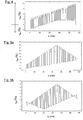
- FIGS. 2 to 5 Detailed descriptions of corresponding superlattices in which the content of at least one element (in this case Al and / or In) varies within layers of one or more types in the superlattice will be described below in connection with the embodiments and comparative examples FIGS. 2 to 5 given.
- FIGS. 2 to 5 In each case, in various embodiments and comparative examples of a superlattice, a respective diagram is shown in which the Al content c Al and optionally the In content c In in percent (ordinate) depending on a vertical position z within the superlattice of a semiconductor layer structure (Abscissa) is indicated. As the zero point of the vertical position z within the superlattice, the side of the superlattice facing an active layer is selected. The active layer thus lies to the left of the illustrated region of the superlattice at negative values of the vertical position z.
- FIG. 12 shows a superlattice of a semiconductor layer structure according to a comparative example, in which layers of two different types a, b are alternately stacked. Of each layer type a, b, 30 layers with a layer thickness of 7.5 nm each are provided, so that the superlattice is 450 nm thick in total.
- the layers of type a are GaN layers.
- the layers of type b are AlGaN layers, wherein the Al content c Al of these layers increases linearly from about 5% to 20% from layer to layer and wherein the Al content c Al is graded within the individual AlGaN layers. The average Al content of the AlGaN layers is thus 12.5%.
- the layer facing the active layer in this case has the lowest Al content c Al .
- the superlattice induces FIG. 2a less stress in the active layer, since the lattice structure and - constants in the superlattice change favorably with the falling down to the active layer Al content.
- An Al content which decreases towards the active layer may furthermore be preferred because transition barriers to the active layer are lowered and thus a heterostructure transition is less pronounced.
- a graded Al content within a layer can aid the conductivity-enhancing effect of a superlattice.
- an in-situ depth determination can take place via the relationship between Al content c Al of the layers in the superlattice and their position within the superlattice.
- a measurement of the Al content of the removed material can be carried out, for example, by mass spectrometry.
- FIG. 2b shows an embodiment of a GaN / AlGaN superlattice, in which the Al content c Al in the AlGaN layers inside the superlattice has a maximum value of about 17% and drops to both sides. In this way, stresses on both sides of the superlattice are reduced, wherein in the example shown the maximum value is not reached exactly in the middle of the superlattice and the layer closest to an active layer has a lower Al content c Al than that of the active layer on furthest removed layer.
- the course of the Al content c Al within a superlattice can be described by an (envelope) function which specifies the Al content c Al of a layer as a function of the position of the layer.
- an (envelope) function which specifies the Al content c Al of a layer as a function of the position of the layer.
- a common function for all types of layers a, b, etc. may be specified, or it may be given a separate function for each layer type.
- any desired, eg non-linear, function course is possible.
- FIG. 3 are comparative examples of superlattices of a semiconductor layer structure in which layers of three different types a, b and c are stacked alternately.
- the layers of type a are in the example of FIG. 3a GaN layers of constant composition over the superlattice.
- the layers of layer types b and c are AlGaN layers whose Al content c Al varies within the superlattice.
- the Al content c Al increases linearly with increasing vertical position z of the layer, however, a type c layer has 2% more Al than the layer directly adjacent to it of type b.
- layers of type b and c are only half as thick as layers of type a.
- the structure can also be considered as a GaN / AlGaN superlattice with only two types of layers, of which the AlGaN layers are graded with a step function.
- a graded Al content within a layer can aid the conductivity-increasing effect of a superlattice.
- the AlGaN layers of the type b and c are carried out as in the example of FIG. 3a , As layers of type a, however, InGaN layers with variable In content c In are provided.
- In the examples of FIG. 3b and 3c follows the In content c In a step function, in the first case with a constant In content within a layer, in the second case with a graded In content.
- the In content c In decreases linearly within 6 layers and is zero for the remaining layers.
- GaN layers can lead to a reduction of induced stress in the active layer, but on the other hand, deteriorate waveguiding by the superlattice, because a higher In content increases the refractive index of the superlattice, resulting in a lower refractive index contrast to an adjacent waveguide layer.
- the non-constant In content c In which is greater in the direction of the active layer, enhances the positive effects of InGaN layers in the superlattice over the adverse effects.
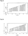
- FIG. 4 shows a comparative example of a superlattice of a semiconductor layer structure in which layers of four different types a, b, c and d are stacked alternately.
- the layers of c and d are similar to layers b and c FIG. 3 AlGaN layers whose Al content c Al linearly increases within the superlattice within the layers of one type, the Al content c Al of a type d layer being about 2% higher than that of the adjacent c type layer, respectively ,
- the In content c In ie the coefficient x, initially decreases linearly in the first 9 layers of the type a and the first 8 layers of the type b (calculated from an active layer) and is zero in the following layers.
- the Al content c Al ie the coefficient y, is zero in the first 8 or 9 layers (z between 0 and 130 nm), then increases linearly for the following middle layers (z between 130 and 270 nm), for the remaining layers (z> 270 nm) at a constant Level to stay.
- the structure can also be considered as a superlattice with only two types of layers, of which the AlGaN layers are graded with a step function.
- the advantages that have a low Al content c Al and an increased In content c In in layers that are directly or indirectly adjacent to the active layer with respect to induced strain are in this embodiment with the positive effects of a (gradual) graded Al content combined to the conductivity of the superlattice.
- FIG. 5 Exemplary embodiments of AlGaN / AlGaN superlattices of a semiconductor layer structure are shown.
- the layers of both types a and b are AlGaN layers in which the Al content c Al varies within the superlattice.
- the Al content c Al depending on the vertical position z of a layer of the type a is described by a first function
- the Al content c Al of a layer of the type b is given by a second function.
- the first function unlike the second.
- Directly adjacent layers thus differ in their Al content c Al and thus in their composition. However, this does not mean that a layer of type a can not have the same composition as a layer of type b.
- the first function is a function that increases linearly with the vertical position z.
- FIG. 5 is created by the varying in both types of layers a and b Al content c Al a superlattice, which allows a good waveguide by a high average Al content and yet by the falling to the active layer Al content c Al tensions on the active layer reasonably low.
Claims (12)
- Composant optoélectronique qui comporte une couche active (6), dans lequel- la couche active (6) est disposée entre des couches de guide d'ondes (5, 8),- une couche barrière (7) est disposée entre la couche active (6) et l'une des couches de guide d'ondes (8),- une couche de revêtement est respectivement disposée sur le côté des couches de guide d'ondes qui est opposé à la couche active, au moins une couche de revêtement comprend une structure de couche semi-conductrice, qui comprend un super-réseau (9) constitué de couches empilées (9a, 9b) d'un premier (a) et d'au moins un deuxième type (b),- les couches (9a, 9b) du premier type (a) et de l'au moins un deuxième type (b) sont des couches empilées de manière alternée d'InxAlyGa1-x-yN et d'InwAlzGa1-w-zN, avec 0 ≤ x, y, w, z ≤ 1 et x + y ≤ 1 et w + z ≤ 1,- dans le super-réseau (9) des couches voisines de type différent diffèrent par leur composition en au moins un élément,- dans le super-réseau (9) au moins deux couches d'un même type présentent une teneur différente (cAl, cIn) en l'au moins un élément,- la teneur (cAl, cIn) en l'au moins un élément des couches (9a, 9b) d'au moins un type (a, b) est amenée à varier progressivement à l'intérieur du super-réseau (9),- les couches (9a, 9b) du super-réseau (9) contiennent des matériaux dopants à des concentrations prédéterminées, dans lequel le super-réseau (9) comporte des couches (9a, 9b) qui sont dopées par du Mg à des concentrations différentes, et- la teneur (cAl, cIn) en l'au moins un élément à l'intérieur du super-réseau présente une valeur maximale qui ne se situe pas au centre du super-réseau.
- Composant optoélectronique selon la revendication 1, dans lequel une position verticale (z) à l'intérieur de la structure de couche semi-conductrice est associée à des couches individuelles du super-réseau (9), et la teneur (cAl, cIn) en l'au moins un élément dans une couche dépend de manière prédéterminée de sa position verticale (z) à l'intérieur de la structure de couche semi-conductrice.
- Composant optoélectronique selon la revendication 2, dans lequel la dépendance de la teneur (cAl, cIn) en l'au moins un élément est prédéterminée par une fonction commune de la position verticale (z) pour toutes les couches (9a, 9b) du super-réseau (9).
- Composant optoélectronique selon la revendication 2, dans lequel la dépendance de la teneur (cAl, cIn) en l'au moins un élément, pour les couches (9a) du premier type (a) est prédéterminée par une première fonction et, pour les couches (9b) de l'au moins un deuxième type (b), est prédéterminée par au moins une deuxième fonction de la position verticale (z).
- Composant optoélectronique selon la revendication 4, dans lequel la première fonction est une fonction discontinue ou une fonction croissant ou décroissant de manière monotone ou une fonction linéaire ou une fonction polynomiale ou une fonction exponentielle ou une fonction logarithmique ou une fonction périodique ou une superposition desdites fonctions ou contient des parties de l'une desdites fonctions.
- Composant optoélectronique selon l'une quelconque des revendications 4 ou 5, dans lequel l'au moins une deuxième fonction est une fonction discontinue ou une fonction croissant ou décroissant de manière monotone ou une fonction linéaire ou une fonction polynomiale ou une fonction exponentielle ou une fonction logarithmique ou une fonction périodique ou une superposition desdites fonctions ou contient des parties de l'une desdites fonctions.
- Composant optoélectronique selon la revendication 3, dans lequel la fonction commune est une fonction discontinue ou une fonction croissant ou décroissant de manière monotone ou une fonction linéaire ou une fonction polynomiale ou une fonction exponentielle ou une fonction logarithmique ou une fonction périodique ou une superposition desdites fonctions ou contient des parties de l'une desdites fonctions.
- Composant optoélectronique selon l'une quelconque des revendications 1 à 7, dans lequel la teneur (cAl, cIn) en l'au moins un élément est constante à l'intérieur de la couche (9a, 9b) du super-réseau (9).
- Composant optoélectronique selon l'une quelconque des revendications 1 à 8, dans lequel toutes les couches (9a, 9b) ont les mêmes épaisseurs.
- Composant optoélectronique selon l'une quelconque des revendications 1 à 8, dans lequel des couches (9a, 9b) de type différent (a, b) ont des épaisseurs différentes.
- Composant optoélectronique selon l'une quelconque des revendications précédentes, qui est une diode électroluminescente.
- Composant optoélectronique selon l'une quelconque des revendications précédentes 1 à 10, qui est une diode laser.
Applications Claiming Priority (2)
| Application Number | Priority Date | Filing Date | Title |
|---|---|---|---|
| DE102006034820 | 2006-07-27 | ||
| DE102006046237A DE102006046237A1 (de) | 2006-07-27 | 2006-09-29 | Halbleiter-Schichtstruktur mit Übergitter |
Publications (2)
| Publication Number | Publication Date |
|---|---|
| EP1883141A1 EP1883141A1 (fr) | 2008-01-30 |
| EP1883141B1 true EP1883141B1 (fr) | 2017-05-24 |
Family
ID=38542049
Family Applications (1)
| Application Number | Title | Priority Date | Filing Date |
|---|---|---|---|
| EP07013822.7A Expired - Fee Related EP1883141B1 (fr) | 2006-07-27 | 2007-07-13 | LD ou DEL avec une couche de revêtement superréseau |
Country Status (3)
| Country | Link |
|---|---|
| US (2) | US7893424B2 (fr) |
| EP (1) | EP1883141B1 (fr) |
| JP (1) | JP2008034851A (fr) |
Families Citing this family (48)
| Publication number | Priority date | Publication date | Assignee | Title |
|---|---|---|---|---|
| US20060039498A1 (en) * | 2004-08-19 | 2006-02-23 | De Figueiredo Rui J P | Pre-distorter for orthogonal frequency division multiplexing systems and method of operating the same |
| EP1883119B1 (fr) | 2006-07-27 | 2015-11-04 | OSRAM Opto Semiconductors GmbH | Structure de recouvrement semi-conductrice dotée d'une surgrille |
| EP1883141B1 (fr) | 2006-07-27 | 2017-05-24 | OSRAM Opto Semiconductors GmbH | LD ou DEL avec une couche de revêtement superréseau |
| EP1883140B1 (fr) | 2006-07-27 | 2013-02-27 | OSRAM Opto Semiconductors GmbH | LD ou DEL avec une couche de revêtment superréseau et dopage gradué |
| US8563995B2 (en) * | 2008-03-27 | 2013-10-22 | Nitek, Inc. | Ultraviolet light emitting diode/laser diode with nested superlattice |
| DE102008030584A1 (de) | 2008-06-27 | 2009-12-31 | Osram Opto Semiconductors Gmbh | Verfahren zur Herstellung eines optoelektronischen Bauelementes und optoelektronisches Bauelement |
| JP5167081B2 (ja) * | 2008-11-13 | 2013-03-21 | パナソニック株式会社 | 窒化物半導体デバイス |
| DE102009037416B4 (de) | 2009-08-13 | 2021-10-14 | OSRAM Opto Semiconductors Gesellschaft mit beschränkter Haftung | Elektrisch gepumpter optoelektronischer Halbleiterchip |
| JP5743893B2 (ja) * | 2009-09-28 | 2015-07-01 | 株式会社トクヤマ | 積層体の製造方法 |
| US8389977B2 (en) | 2009-12-10 | 2013-03-05 | Transphorm Inc. | Reverse side engineered III-nitride devices |
| KR101408610B1 (ko) * | 2009-12-21 | 2014-06-17 | 가부시끼가이샤 도시바 | 질화물 반도체 발광 소자 및 그 제조 방법 |
| DE102009060749B4 (de) | 2009-12-30 | 2021-12-30 | OSRAM Opto Semiconductors Gesellschaft mit beschränkter Haftung | Optoelektronischer Halbleiterchip |
| FR2957718B1 (fr) * | 2010-03-16 | 2012-04-20 | Commissariat Energie Atomique | Diode electroluminescente hybride a rendement eleve |
| US8742460B2 (en) | 2010-12-15 | 2014-06-03 | Transphorm Inc. | Transistors with isolation regions |
| US8643062B2 (en) | 2011-02-02 | 2014-02-04 | Transphorm Inc. | III-N device structures and methods |
| US8358673B2 (en) * | 2011-02-17 | 2013-01-22 | Corning Incorporated | Strain balanced laser diode |
| EP2681816A1 (fr) * | 2011-02-28 | 2014-01-08 | Corning Incorporated | Lasers à semi-conducteurs à couches de revêtement contenant de l'indium |
| US8901604B2 (en) | 2011-09-06 | 2014-12-02 | Transphorm Inc. | Semiconductor devices with guard rings |
| US9257547B2 (en) | 2011-09-13 | 2016-02-09 | Transphorm Inc. | III-N device structures having a non-insulating substrate |
| US8598937B2 (en) | 2011-10-07 | 2013-12-03 | Transphorm Inc. | High power semiconductor electronic components with increased reliability |
| KR20130079873A (ko) * | 2012-01-03 | 2013-07-11 | 엘지이노텍 주식회사 | 발광소자 및 이를 포함하는 조명시스템 |
| CN102544281A (zh) * | 2012-01-20 | 2012-07-04 | 厦门市三安光电科技有限公司 | 具有多层势垒结构的氮化镓基发光二极管 |
| US9165766B2 (en) * | 2012-02-03 | 2015-10-20 | Transphorm Inc. | Buffer layer structures suited for III-nitride devices with foreign substrates |
| WO2013155108A1 (fr) | 2012-04-09 | 2013-10-17 | Transphorm Inc. | Transistors au nitrure-iii n-polaires |
| US9219189B2 (en) | 2012-09-14 | 2015-12-22 | Palo Alto Research Center Incorporated | Graded electron blocking layer |
| US9401452B2 (en) * | 2012-09-14 | 2016-07-26 | Palo Alto Research Center Incorporated | P-side layers for short wavelength light emitters |
| KR101936312B1 (ko) * | 2012-10-09 | 2019-01-08 | 엘지이노텍 주식회사 | 발광소자 |
| KR102042181B1 (ko) * | 2012-10-22 | 2019-11-07 | 엘지이노텍 주식회사 | 발광소자 |
| JP2014143338A (ja) * | 2013-01-25 | 2014-08-07 | Sharp Corp | 窒化物半導体発光素子 |
| US9087718B2 (en) | 2013-03-13 | 2015-07-21 | Transphorm Inc. | Enhancement-mode III-nitride devices |
| US9245993B2 (en) | 2013-03-15 | 2016-01-26 | Transphorm Inc. | Carbon doping semiconductor devices |
| KR20140117117A (ko) * | 2013-03-26 | 2014-10-07 | 인텔렉추얼디스커버리 주식회사 | 질화물 반도체 발광소자 |
| WO2015009514A1 (fr) | 2013-07-19 | 2015-01-22 | Transphorm Inc. | Transistor au nitrure iii comprenant une couche d'appauvrissement de type p |
| US9318593B2 (en) | 2014-07-21 | 2016-04-19 | Transphorm Inc. | Forming enhancement mode III-nitride devices |
| KR102237111B1 (ko) * | 2014-07-28 | 2021-04-08 | 엘지이노텍 주식회사 | 발광소자 및 조명시스템 |
| FR3028670B1 (fr) * | 2014-11-18 | 2017-12-22 | Commissariat Energie Atomique | Structure semi-conductrice a couche de semi-conducteur du groupe iii-v ou ii-vi comprenant une structure cristalline a mailles cubiques ou hexagonales |
| US9536966B2 (en) | 2014-12-16 | 2017-01-03 | Transphorm Inc. | Gate structures for III-N devices |
| US9536967B2 (en) | 2014-12-16 | 2017-01-03 | Transphorm Inc. | Recessed ohmic contacts in a III-N device |
| TWI577046B (zh) * | 2014-12-23 | 2017-04-01 | 錼創科技股份有限公司 | 半導體發光元件及其製作方法 |
| US9673352B2 (en) * | 2015-04-30 | 2017-06-06 | National Chiao Tung University | Semiconductor light emitting device |
| WO2017123999A1 (fr) | 2016-01-15 | 2017-07-20 | Transphorm Inc. | Dispositifs en nitrure iii à mode de perfectionnement ayant un isolant de grille en al(1-x)sixo |
| US10224401B2 (en) | 2016-05-31 | 2019-03-05 | Transphorm Inc. | III-nitride devices including a graded depleting layer |
| DE102017119931A1 (de) * | 2017-08-30 | 2019-02-28 | Osram Opto Semiconductors Gmbh | Optoelektronisches Halbleiterbauelement |
| US10516076B2 (en) | 2018-02-01 | 2019-12-24 | Silanna UV Technologies Pte Ltd | Dislocation filter for semiconductor devices |
| US10879420B2 (en) | 2018-07-09 | 2020-12-29 | University Of Iowa Research Foundation | Cascaded superlattice LED system |
| CN110600591B (zh) * | 2019-08-21 | 2021-11-26 | 苏州紫灿科技有限公司 | 具有啁啾超晶格最终势垒结构的深紫外led及制备方法 |
| EP4042530A4 (fr) * | 2019-09-30 | 2023-10-25 | NLIGHT, Inc. | Couche de gainage modifiée par contrainte pour une déformation de région active optimisée et des performances de diode laser améliorées |
| US11322647B2 (en) | 2020-05-01 | 2022-05-03 | Silanna UV Technologies Pte Ltd | Buried contact layer for UV emitting device |
Family Cites Families (75)
| Publication number | Priority date | Publication date | Assignee | Title |
|---|---|---|---|---|
| JPS60145686A (ja) | 1984-01-09 | 1985-08-01 | Nec Corp | 半導体レ−ザ |
| US4839899A (en) * | 1988-03-09 | 1989-06-13 | Xerox Corporation | Wavelength tuning of multiple quantum well (MQW) heterostructure lasers |
| US4882734A (en) | 1988-03-09 | 1989-11-21 | Xerox Corporation | Quantum well heterostructure lasers with low current density threshold and higher TO values |
| JPH01241192A (ja) | 1988-03-23 | 1989-09-26 | Fujitsu Ltd | 半導体装置 |
| US4961197A (en) | 1988-09-07 | 1990-10-02 | Hitachi, Ltd. | Semiconductor laser device |
| CA1299719C (fr) | 1989-01-13 | 1992-04-28 | Hui Chun Liu | Source infrarouge a super-reseau semiconducteur |
| US5060028A (en) | 1989-01-19 | 1991-10-22 | Hewlett-Packard Company | High band-gap opto-electronic device |
| US4984242A (en) * | 1989-09-18 | 1991-01-08 | Spectra Diode Laboratories, Inc. | GaAs/AlGaAs heterostructure laser containing indium |
| US5319657A (en) | 1991-10-08 | 1994-06-07 | Matsushita Electric Industrial Co., Ltd. | Semiconductor laser of modulation doping quantum well structure with stopper against dopant dispersion and manufacturing method thereof |
| US5198682A (en) | 1991-11-12 | 1993-03-30 | Hughes Aircraft Company | Multiple quantum well superlattice infrared detector with graded conductive band |
| JPH0794829A (ja) | 1993-04-05 | 1995-04-07 | Matsushita Electric Ind Co Ltd | 半導体レーザ |
| US5395793A (en) | 1993-12-23 | 1995-03-07 | National Research Council Of Canada | Method of bandgap tuning of semiconductor quantum well structures |
| US5570386A (en) | 1994-04-04 | 1996-10-29 | Lucent Technologies Inc. | Semiconductor laser |
| US5751013A (en) * | 1994-07-21 | 1998-05-12 | Matsushita Electric Industrial Co., Ltd. | Semiconductor light-emitting device and production method thereof |
| US5497012A (en) | 1994-06-15 | 1996-03-05 | Hewlett-Packard Company | Unipolar band minima devices |
| US5670798A (en) | 1995-03-29 | 1997-09-23 | North Carolina State University | Integrated heterostructures of Group III-V nitride semiconductor materials including epitaxial ohmic contact non-nitride buffer layer and methods of fabricating same |
| US5588015A (en) | 1995-08-22 | 1996-12-24 | University Of Houston | Light emitting devices based on interband transitions in type-II quantum well heterostructures |
| JPH1022524A (ja) | 1996-07-02 | 1998-01-23 | Omron Corp | 半導体発光素子 |
| US5936989A (en) | 1997-04-29 | 1999-08-10 | Lucent Technologies, Inc. | Quantum cascade laser |
| KR100688240B1 (ko) | 1997-01-09 | 2007-03-02 | 니치아 카가쿠 고교 가부시키가이샤 | 질화물반도체소자 |
| US6677619B1 (en) | 1997-01-09 | 2004-01-13 | Nichia Chemical Industries, Ltd. | Nitride semiconductor device |
| JP3282175B2 (ja) * | 1997-02-04 | 2002-05-13 | 日亜化学工業株式会社 | 窒化物半導体素子 |
| JP3014339B2 (ja) | 1997-04-25 | 2000-02-28 | カナレ電気株式会社 | 量子波干渉層を有した半導体素子 |
| JP3642157B2 (ja) | 1997-05-26 | 2005-04-27 | ソニー株式会社 | p型III族ナイトライド化合物半導体、発光ダイオードおよび半導体レーザ |
| WO1999005728A1 (fr) | 1997-07-25 | 1999-02-04 | Nichia Chemical Industries, Ltd. | Dispositif a semi-conducteur en nitrure |
| JPH1168158A (ja) | 1997-08-20 | 1999-03-09 | Sanyo Electric Co Ltd | 窒化ガリウム系化合物半導体装置 |
| JP3468082B2 (ja) | 1998-02-26 | 2003-11-17 | 日亜化学工業株式会社 | 窒化物半導体素子 |
| JPH11340505A (ja) * | 1998-05-25 | 1999-12-10 | Matsushita Electric Ind Co Ltd | 窒化ガリウム系化合物半導体発光素子 |
| JP2000091708A (ja) | 1998-09-14 | 2000-03-31 | Toshiba Corp | 半導体発光素子 |
| JP2000286451A (ja) | 1998-11-17 | 2000-10-13 | Nichia Chem Ind Ltd | 窒化物半導体素子 |
| JP2000244070A (ja) | 1999-02-19 | 2000-09-08 | Sony Corp | 半導体装置および半導体発光素子 |
| WO2000058999A2 (fr) | 1999-03-26 | 2000-10-05 | Matsushita Electric Industrial Co., Ltd. | Structures de semi-conducteur possedant une couche a contraintes compensees et procede de fabrication associe |
| GB9913950D0 (en) | 1999-06-15 | 1999-08-18 | Arima Optoelectronics Corp | Unipolar light emitting devices based on iii-nitride semiconductor superlattices |
| DE19955747A1 (de) * | 1999-11-19 | 2001-05-23 | Osram Opto Semiconductors Gmbh | Optische Halbleitervorrichtung mit Mehrfach-Quantentopf-Struktur |
| US6441393B2 (en) | 1999-11-17 | 2002-08-27 | Lumileds Lighting U.S., Llc | Semiconductor devices with selectively doped III-V nitride layers |
| JP2001168385A (ja) | 1999-12-06 | 2001-06-22 | Toyoda Gosei Co Ltd | Iii族窒化物系化合物半導体素子及びiii族窒化物系化合物半導体発光素子 |
| US6535536B2 (en) | 2000-04-10 | 2003-03-18 | Fuji Photo Film Co., Ltd. | Semiconductor laser element |
| JP2002057410A (ja) * | 2000-05-29 | 2002-02-22 | Fuji Photo Film Co Ltd | 半導体レーザ素子 |
| US6556604B1 (en) | 2000-11-08 | 2003-04-29 | Lucent Technologies Inc. | Flat minibands with spatially symmetric wavefunctions in intersubband superlattice light emitters |
| JP3453558B2 (ja) | 2000-12-25 | 2003-10-06 | 松下電器産業株式会社 | 窒化物半導体素子 |
| KR100906760B1 (ko) | 2001-03-28 | 2009-07-09 | 니치아 카가쿠 고교 가부시키가이샤 | 질화물 반도체 소자 |
| US6489636B1 (en) | 2001-03-29 | 2002-12-03 | Lumileds Lighting U.S., Llc | Indium gallium nitride smoothing structures for III-nitride devices |
| US6649942B2 (en) | 2001-05-23 | 2003-11-18 | Sanyo Electric Co., Ltd. | Nitride-based semiconductor light-emitting device |
| US6630692B2 (en) | 2001-05-29 | 2003-10-07 | Lumileds Lighting U.S., Llc | III-Nitride light emitting devices with low driving voltage |
| US7692182B2 (en) | 2001-05-30 | 2010-04-06 | Cree, Inc. | Group III nitride based quantum well light emitting device structures with an indium containing capping structure |
| US6958497B2 (en) | 2001-05-30 | 2005-10-25 | Cree, Inc. | Group III nitride based light emitting diode structures with a quantum well and superlattice, group III nitride based quantum well structures and group III nitride based superlattice structures |
| JP2003008058A (ja) | 2001-06-18 | 2003-01-10 | Showa Denko Kk | AlGaInPエピタキシャルウエーハ及びそれを製造する方法並びにそれを用いた半導体発光素子 |
| JP4057802B2 (ja) | 2001-09-05 | 2008-03-05 | 株式会社日立製作所 | 半導体光素子 |
| WO2003041234A1 (fr) | 2001-11-05 | 2003-05-15 | Nichia Corporation | Element semi-conducteur |
| US6618413B2 (en) | 2001-12-21 | 2003-09-09 | Xerox Corporation | Graded semiconductor layers for reducing threshold voltage for a nitride-based laser diode structure |
| US7919791B2 (en) | 2002-03-25 | 2011-04-05 | Cree, Inc. | Doped group III-V nitride materials, and microelectronic devices and device precursor structures comprising same |
| GB0207307D0 (en) | 2002-03-27 | 2002-05-08 | Koninkl Philips Electronics Nv | In-pixel memory for display devices |
| JP4204982B2 (ja) * | 2002-04-04 | 2009-01-07 | シャープ株式会社 | 半導体レーザ素子 |
| JP4119158B2 (ja) * | 2002-04-23 | 2008-07-16 | 三菱電機株式会社 | 傾斜状多重量子バリアを用いた半導体発光素子 |
| JP3755084B2 (ja) | 2002-04-24 | 2006-03-15 | 中東産業株式会社 | 蝶番 |
| JP4221697B2 (ja) | 2002-06-17 | 2009-02-12 | 日本電気株式会社 | 半導体装置 |
| US20030235224A1 (en) | 2002-06-19 | 2003-12-25 | Ohlander Ulf Roald | Strained quantum-well structure having ternary-alloy material in both quantum-well layers and barrier layers |
| GB2396054B (en) | 2002-11-20 | 2006-01-11 | Intense Photonics Ltd | Semiconductor optical device with beam focusing |
| GB0306279D0 (en) | 2003-03-19 | 2003-04-23 | Bookham Technology Plc | High power semiconductor laser with large optical superlattice waveguide |
| US7609737B2 (en) * | 2003-07-10 | 2009-10-27 | Nichia Corporation | Nitride semiconductor laser element |
| KR100580623B1 (ko) | 2003-08-04 | 2006-05-16 | 삼성전자주식회사 | 초격자 구조의 반도체층을 갖는 반도체 소자 및 그 제조방법 |
| TWI228320B (en) | 2003-09-09 | 2005-02-21 | Ind Tech Res Inst | An avalanche photo-detector(APD) with high saturation power, high gain-bandwidth product |
| EP1670106A4 (fr) | 2003-09-25 | 2007-12-12 | Matsushita Electric Ind Co Ltd | Dispositif semi-conducteur en nitrure et procede de fabrication de celui-ci |
| US20050162616A1 (en) * | 2004-01-23 | 2005-07-28 | Hewlett-Packard Co. | System and method of contrast enhancement in digital projectors |
| DE102004009531B4 (de) | 2004-02-20 | 2007-03-01 | Forschungszentrum Rossendorf E.V. | Quanten-Kaskaden-Laser-Struktur |
| US7294868B2 (en) | 2004-06-25 | 2007-11-13 | Finisar Corporation | Super lattice tunnel junctions |
| KR100662191B1 (ko) | 2004-12-23 | 2006-12-27 | 엘지이노텍 주식회사 | 질화물 반도체 발광소자 및 그 제조방법 |
| US7885306B2 (en) * | 2006-06-30 | 2011-02-08 | Osram Opto Semiconductors Gmbh | Edge-emitting semiconductor laser chip |
| DE102006046228A1 (de) * | 2006-07-27 | 2008-01-31 | Osram Opto Semiconductors Gmbh | Halbleiter-Schichtstruktur mit Übergitter |
| EP1883140B1 (fr) * | 2006-07-27 | 2013-02-27 | OSRAM Opto Semiconductors GmbH | LD ou DEL avec une couche de revêtment superréseau et dopage gradué |
| DE102006046237A1 (de) | 2006-07-27 | 2008-01-31 | Osram Opto Semiconductors Gmbh | Halbleiter-Schichtstruktur mit Übergitter |
| EP1883141B1 (fr) * | 2006-07-27 | 2017-05-24 | OSRAM Opto Semiconductors GmbH | LD ou DEL avec une couche de revêtement superréseau |
| EP1883119B1 (fr) * | 2006-07-27 | 2015-11-04 | OSRAM Opto Semiconductors GmbH | Structure de recouvrement semi-conductrice dotée d'une surgrille |
| US7547908B2 (en) * | 2006-12-22 | 2009-06-16 | Philips Lumilieds Lighting Co, Llc | III-nitride light emitting devices grown on templates to reduce strain |
| DE102010009457A1 (de) * | 2010-02-26 | 2011-09-01 | Osram Opto Semiconductors Gmbh | Optoelektronischer Halbleiterchip |
-
2007
- 2007-07-13 EP EP07013822.7A patent/EP1883141B1/fr not_active Expired - Fee Related
- 2007-07-20 US US11/780,514 patent/US7893424B2/en not_active Expired - Fee Related
- 2007-07-27 JP JP2007195432A patent/JP2008034851A/ja active Pending
-
2011
- 2011-01-19 US US13/009,422 patent/US8471240B2/en active Active
Also Published As
| Publication number | Publication date |
|---|---|
| JP2008034851A (ja) | 2008-02-14 |
| US8471240B2 (en) | 2013-06-25 |
| EP1883141A1 (fr) | 2008-01-30 |
| US20080054247A1 (en) | 2008-03-06 |
| US7893424B2 (en) | 2011-02-22 |
| US20110168977A1 (en) | 2011-07-14 |
Similar Documents
| Publication | Publication Date | Title |
|---|---|---|
| EP1883141B1 (fr) | LD ou DEL avec une couche de revêtement superréseau | |
| EP1883140B1 (fr) | LD ou DEL avec une couche de revêtment superréseau et dopage gradué | |
| EP2212931B1 (fr) | Led comportant une couche de diffusion de courant | |
| EP2165374B1 (fr) | Corps semi-conducteur émetteur de rayonnement | |
| EP2208240B1 (fr) | Puce semi-conductrice optoélectronique à structure de puits quantiques multiples | |
| DE102009060747A1 (de) | Halbleiterchip | |
| WO2018050466A1 (fr) | Série de couches semi-conductrices | |
| WO2009036730A2 (fr) | Puce semi-conductrice optoélectronique à structure à puits quantiques | |
| DE102011112706A1 (de) | Optoelektronisches Bauelement | |
| EP1883119B1 (fr) | Structure de recouvrement semi-conductrice dotée d'une surgrille | |
| DE102006046237A1 (de) | Halbleiter-Schichtstruktur mit Übergitter | |
| WO2016110433A1 (fr) | Composant optoélectronique | |
| DE102012220911A1 (de) | Halbleiterlaser mit verbesserter Stromführung | |
| DE102013017275B4 (de) | Optoelektronisches Halbleiterbauelement | |
| EP2465148B1 (fr) | Puce semi-conductrice optoélectronique pompée électriquement | |
| DE102016109022A1 (de) | Laserdiodenchip | |
| EP1739758A2 (fr) | Dispositif à semi-conducteur électroluminescent avec barrière contre la diffusion | |
| EP2313935A1 (fr) | Puce semiconductrice optoélectronique | |
| WO2011032841A2 (fr) | Laser à semi-conducteurs à émission par la tranche | |
| EP3345224B1 (fr) | Puce semi-conductrice optoélectronique et procédé de fabrication correspondant | |
| WO2010048918A1 (fr) | Puce de semiconducteur optoélectronique et procédé de fabrication d'une puce de semiconducteur optoélectronique | |
| DE102006046227A1 (de) | Halbleiter-Schichtstruktur mit Übergitter | |
| DE112018005379B4 (de) | Laserdiode | |
| WO2021013740A1 (fr) | Puce semi-conductrice optoélectronique | |
| DE102006046228A1 (de) | Halbleiter-Schichtstruktur mit Übergitter |
Legal Events
| Date | Code | Title | Description |
|---|---|---|---|
| PUAI | Public reference made under article 153(3) epc to a published international application that has entered the european phase |
Free format text: ORIGINAL CODE: 0009012 |
|
| AK | Designated contracting states |
Kind code of ref document: A1 Designated state(s): AT BE BG CH CY CZ DE DK EE ES FI FR GB GR HU IE IS IT LI LT LU LV MC MT NL PL PT RO SE SI SK TR |
|
| AX | Request for extension of the european patent |
Extension state: AL BA HR MK YU |
|
| RAP1 | Party data changed (applicant data changed or rights of an application transferred) |
Owner name: OSRAM OPTO SEMICONDUCTORS GMBH |
|
| RAP1 | Party data changed (applicant data changed or rights of an application transferred) |
Owner name: OSRAM OPTO SEMICONDUCTORS GMBH |
|
| 17P | Request for examination filed |
Effective date: 20080707 |
|
| 17Q | First examination report despatched |
Effective date: 20080822 |
|
| AKX | Designation fees paid |
Designated state(s): DE |
|
| GRAP | Despatch of communication of intention to grant a patent |
Free format text: ORIGINAL CODE: EPIDOSNIGR1 |
|
| RIC1 | Information provided on ipc code assigned before grant |
Ipc: H01S 5/32 20060101ALN20161013BHEP Ipc: H01L 33/32 20100101ALI20161013BHEP Ipc: H01S 5/20 20060101ALN20161013BHEP Ipc: H01S 5/343 20060101AFI20161013BHEP Ipc: H01L 33/04 20100101ALN20161013BHEP Ipc: H01S 5/042 20060101ALN20161013BHEP Ipc: H01L 33/06 20100101ALI20161013BHEP Ipc: H01S 5/30 20060101ALN20161013BHEP |
|
| RIC1 | Information provided on ipc code assigned before grant |
Ipc: H01L 33/06 20100101ALI20161019BHEP Ipc: H01S 5/30 20060101ALN20161019BHEP Ipc: H01S 5/042 20060101ALN20161019BHEP Ipc: H01L 33/32 20100101ALI20161019BHEP Ipc: H01S 5/343 20060101AFI20161019BHEP Ipc: H01L 33/04 20100101ALN20161019BHEP Ipc: H01S 5/20 20060101ALN20161019BHEP Ipc: H01S 5/32 20060101ALN20161019BHEP |
|
| INTG | Intention to grant announced |
Effective date: 20161104 |
|
| RIN1 | Information on inventor provided before grant (corrected) |
Inventor name: LELL, ALFRED Inventor name: SCHILLGALIES, MARC Inventor name: EICHLER, CHRISTOPH Inventor name: MILER, ANDREAS |
|
| GRAS | Grant fee paid |
Free format text: ORIGINAL CODE: EPIDOSNIGR3 |
|
| RIN1 | Information on inventor provided before grant (corrected) |
Inventor name: EICHLER, CHRISTOPH Inventor name: SCHILLGALIES, MARC Inventor name: LELL, ALFRED Inventor name: MILER, ANDREAS |
|
| GRAA | (expected) grant |
Free format text: ORIGINAL CODE: 0009210 |
|
| AK | Designated contracting states |
Kind code of ref document: B1 Designated state(s): DE |
|
| REG | Reference to a national code |
Ref country code: DE Ref legal event code: R096 Ref document number: 502007015661 Country of ref document: DE |
|
| REG | Reference to a national code |
Ref country code: DE Ref legal event code: R097 Ref document number: 502007015661 Country of ref document: DE |
|
| PLBE | No opposition filed within time limit |
Free format text: ORIGINAL CODE: 0009261 |
|
| STAA | Information on the status of an ep patent application or granted ep patent |
Free format text: STATUS: NO OPPOSITION FILED WITHIN TIME LIMIT |
|
| 26N | No opposition filed |
Effective date: 20180227 |
|
| PGFP | Annual fee paid to national office [announced via postgrant information from national office to epo] |
Ref country code: DE Payment date: 20210721 Year of fee payment: 15 |
|
| REG | Reference to a national code |
Ref country code: DE Ref legal event code: R119 Ref document number: 502007015661 Country of ref document: DE |
|
| PG25 | Lapsed in a contracting state [announced via postgrant information from national office to epo] |
Ref country code: DE Free format text: LAPSE BECAUSE OF NON-PAYMENT OF DUE FEES Effective date: 20230201 |