EP1873833A1 - Thin film transistor array substrate and method of fabricating the same - Google Patents
Thin film transistor array substrate and method of fabricating the same Download PDFInfo
- Publication number
- EP1873833A1 EP1873833A1 EP07011733A EP07011733A EP1873833A1 EP 1873833 A1 EP1873833 A1 EP 1873833A1 EP 07011733 A EP07011733 A EP 07011733A EP 07011733 A EP07011733 A EP 07011733A EP 1873833 A1 EP1873833 A1 EP 1873833A1
- Authority
- EP
- European Patent Office
- Prior art keywords
- passivation film
- gate
- insulating layer
- etching
- electrode
- Prior art date
- Legal status (The legal status is an assumption and is not a legal conclusion. Google has not performed a legal analysis and makes no representation as to the accuracy of the status listed.)
- Withdrawn
Links
Images


Classifications
-
- H—ELECTRICITY
- H10—SEMICONDUCTOR DEVICES; ELECTRIC SOLID-STATE DEVICES NOT OTHERWISE PROVIDED FOR
- H10D—INORGANIC ELECTRIC SEMICONDUCTOR DEVICES
- H10D86/00—Integrated devices formed in or on insulating or conducting substrates, e.g. formed in silicon-on-insulator [SOI] substrates or on stainless steel or glass substrates
-
- G—PHYSICS
- G02—OPTICS
- G02F—OPTICAL DEVICES OR ARRANGEMENTS FOR THE CONTROL OF LIGHT BY MODIFICATION OF THE OPTICAL PROPERTIES OF THE MEDIA OF THE ELEMENTS INVOLVED THEREIN; NON-LINEAR OPTICS; FREQUENCY-CHANGING OF LIGHT; OPTICAL LOGIC ELEMENTS; OPTICAL ANALOGUE/DIGITAL CONVERTERS
- G02F1/00—Devices or arrangements for the control of the intensity, colour, phase, polarisation or direction of light arriving from an independent light source, e.g. switching, gating or modulating; Non-linear optics
- G02F1/01—Devices or arrangements for the control of the intensity, colour, phase, polarisation or direction of light arriving from an independent light source, e.g. switching, gating or modulating; Non-linear optics for the control of the intensity, phase, polarisation or colour
- G02F1/13—Devices or arrangements for the control of the intensity, colour, phase, polarisation or direction of light arriving from an independent light source, e.g. switching, gating or modulating; Non-linear optics for the control of the intensity, phase, polarisation or colour based on liquid crystals, e.g. single liquid crystal display cells
- G02F1/133—Constructional arrangements; Operation of liquid crystal cells; Circuit arrangements
- G02F1/1333—Constructional arrangements; Manufacturing methods
- G02F1/1345—Conductors connecting electrodes to cell terminals
- G02F1/13458—Terminal pads
-
- G—PHYSICS
- G02—OPTICS
- G02F—OPTICAL DEVICES OR ARRANGEMENTS FOR THE CONTROL OF LIGHT BY MODIFICATION OF THE OPTICAL PROPERTIES OF THE MEDIA OF THE ELEMENTS INVOLVED THEREIN; NON-LINEAR OPTICS; FREQUENCY-CHANGING OF LIGHT; OPTICAL LOGIC ELEMENTS; OPTICAL ANALOGUE/DIGITAL CONVERTERS
- G02F1/00—Devices or arrangements for the control of the intensity, colour, phase, polarisation or direction of light arriving from an independent light source, e.g. switching, gating or modulating; Non-linear optics
- G02F1/01—Devices or arrangements for the control of the intensity, colour, phase, polarisation or direction of light arriving from an independent light source, e.g. switching, gating or modulating; Non-linear optics for the control of the intensity, phase, polarisation or colour
- G02F1/13—Devices or arrangements for the control of the intensity, colour, phase, polarisation or direction of light arriving from an independent light source, e.g. switching, gating or modulating; Non-linear optics for the control of the intensity, phase, polarisation or colour based on liquid crystals, e.g. single liquid crystal display cells
- G02F1/133—Constructional arrangements; Operation of liquid crystal cells; Circuit arrangements
- G02F1/136—Liquid crystal cells structurally associated with a semi-conducting layer or substrate, e.g. cells forming part of an integrated circuit
- G02F1/1362—Active matrix addressed cells
- G02F1/136227—Through-hole connection of the pixel electrode to the active element through an insulation layer
-
- H—ELECTRICITY
- H10—SEMICONDUCTOR DEVICES; ELECTRIC SOLID-STATE DEVICES NOT OTHERWISE PROVIDED FOR
- H10D—INORGANIC ELECTRIC SEMICONDUCTOR DEVICES
- H10D86/00—Integrated devices formed in or on insulating or conducting substrates, e.g. formed in silicon-on-insulator [SOI] substrates or on stainless steel or glass substrates
- H10D86/01—Manufacture or treatment
- H10D86/021—Manufacture or treatment of multiple TFTs
- H10D86/0231—Manufacture or treatment of multiple TFTs using masks, e.g. half-tone masks
-
- H—ELECTRICITY
- H10—SEMICONDUCTOR DEVICES; ELECTRIC SOLID-STATE DEVICES NOT OTHERWISE PROVIDED FOR
- H10D—INORGANIC ELECTRIC SEMICONDUCTOR DEVICES
- H10D86/00—Integrated devices formed in or on insulating or conducting substrates, e.g. formed in silicon-on-insulator [SOI] substrates or on stainless steel or glass substrates
- H10D86/40—Integrated devices formed in or on insulating or conducting substrates, e.g. formed in silicon-on-insulator [SOI] substrates or on stainless steel or glass substrates characterised by multiple TFTs
- H10D86/451—Integrated devices formed in or on insulating or conducting substrates, e.g. formed in silicon-on-insulator [SOI] substrates or on stainless steel or glass substrates characterised by multiple TFTs characterised by the compositions or shapes of the interlayer dielectrics
-
- H—ELECTRICITY
- H10—SEMICONDUCTOR DEVICES; ELECTRIC SOLID-STATE DEVICES NOT OTHERWISE PROVIDED FOR
- H10D—INORGANIC ELECTRIC SEMICONDUCTOR DEVICES
- H10D86/00—Integrated devices formed in or on insulating or conducting substrates, e.g. formed in silicon-on-insulator [SOI] substrates or on stainless steel or glass substrates
- H10D86/40—Integrated devices formed in or on insulating or conducting substrates, e.g. formed in silicon-on-insulator [SOI] substrates or on stainless steel or glass substrates characterised by multiple TFTs
- H10D86/60—Integrated devices formed in or on insulating or conducting substrates, e.g. formed in silicon-on-insulator [SOI] substrates or on stainless steel or glass substrates characterised by multiple TFTs wherein the TFTs are in active matrices
Definitions
- the present invention relates to a thin film transistor ("TFT") array substrate and a method of fabricating the same, and more particularly, to a TFT array substrate in which a driving margin may be increased and a sufficiently large contact area between conductive materials may be provided in a contact portion, and a method of fabricating the TFT array substrate.
- TFT thin film transistor
- a liquid crystal display (“LCD”) includes two opposing display panels and a liquid crystal layer interposed therebetween. Each display panel may use a transparent insulating substrate as a supporting substrate. A plurality of thin film patterns may be formed on the insulating substrate. A thin film pattern formation includes a material deposition and a mask process. However, a photolithography process may include multiple steps, such as photoresist coating, mask arrangement, exposure, baking, development, and cleaning, thus increasing the entire processing time and the manufacturing cost.
- a lift-off method has been studied. More specifically, when a passivation film and a pixel electrode are formed on a TFT array substrate, the passivation film is patterned using a photoresist pattern, a conductive material is deposited on the entire surface of the TFT array substrate, and the photoresist pattern and the conductive material thereon are simultaneously removed using a photoresist stripper. The conductive material remaining on the substrate forms a pixel electrode.
- the photoresist stripper may contact the sides or bottom of the photoresist pattern to remove the photoresist pattern covered with the conductive material.
- the contact area of the photoresist pattern with the photoresist stripper should be sufficiently large.
- the passivation film under the photoresist pattern should form a sufficiently large undercut under the inner side of the photoresist pattern.
- an insulating film on a storage electrode may be over-etched and its thickness may become non-uniform, thus causing a reduction in a driving margin.
- a data interconnection line may be damaged by over-etching, and etching of the data interconnection line in a contact area may cause a contact failure.
- This invention provides a TFT array substrate that increases a driving margin and provides a sufficiently large contact area between conductive materials in a contact portion.
- the present invention also provides a TFT array substrate that enables easy lift-off and prevents over-etching of a gate insulating layer and damage to a data interconnection line.
- the present invention discloses a thin film transistor (TFT) array substrate including a gate interconnection line including a gate line and a gate electrode arranged on an insulating substrate, a gate insulating layer covering the gate interconnection line, a semiconductor layer arranged on the gate insulating layer, a data interconnection line including a data line, a source electrode, and a drain electrode arranged on the semiconductor layer, a first passivation film arranged on the data interconnection line and exposing a portion of the drain electrode, a second passivation film arranged on the first passivation film, wherein an outer sidewall of the second passivation film is positioned inside an outer sidewall of the first passivation film, and a pixel electrode connected to the drain electrode.
- TFT thin film transistor
- the present invention also discloses a method of fabricating a thin film transistor (TFT) array substrate, the method including forming a gate interconnection line on an insulating substrate, the gate interconnection line including a gate line and a gate electrode, forming a gate insulating layer on the gate interconnection line, forming a semiconductor layer and a data interconnection line on the semiconductor layer, the data interconnection line including a data line, a source electrode, and a drain electrode, sequentially forming a first passivation film and a second passivation film on the data interconnection line, etching the second passivation film and the first passivation film, and exposing a drain electrode of a drain electrode-pixel electrode contact portion, and forming a pixel electrode connected to the drain electrode. Further, etching the second passivation film and the first passivation film includes forming an outer sidewall of the second passivation film inside an outer sidewall of the first passivation film.
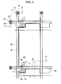
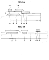
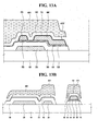
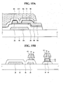
- FIG. 1 is a layout of a TFT array substrate according to a first exemplary embodiment of the present invention.
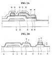
- FIG. 2A is a cross-sectional view taken along line A-A' of FIG. 1.
- FIG. 2B is a cross-sectional view taken along line B-B' of FIG. 1.
- FIG. 2C is a cross-sectional view taken along line C-C' of FIG. 1.
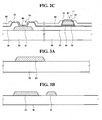
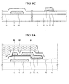
- FIGS. 3A, 4A, 5A, 6A, 7A, 8A, 9A, 10A, and 11A are cross-sectional views showing processing steps of the method of fabricating the TFT array substrate cross-sectional view shown in FIG. 2A according to a second exemplary embodiment of the present invention.
- FIGS. 3B, 4B, 5B, 6B, 7B, 8B, 9B, 10B, and 11B are cross-sectional views showing processing steps of the method of fabricating the TFT array substrate cross-sectional view shown in FIG. 2B according to the second exemplary embodiment of the present invention.
- FIGS. 3C, 4C, 5C, 6C, 7C, 8C, 9C, 10C, and 11C are cross-sectional views showing processing steps of the method of fabricating the TFT array substrate cross-sectional view shown in FIG. 2C according to the second exemplary embodiment of the present invention.
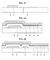
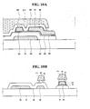
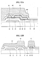
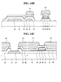
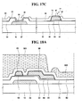
- FIGS. 12A, 13A, 14A, and 15A are cross-sectional views showing processing steps of the method of fabricating the TFT array substrate cross-sectional view shown in FIG. 2A according to the third exemplary embodiment of the present invention.
- FIGS. 12B, 13B, 14B, and 15B are cross-sectional views showing processing steps of the method of fabricating the TFT array substrate cross-sectional view shown in FIG. 2B according to the third exemplary embodiment of the present invention.
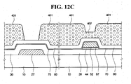
- FIGS. 12C, 13C, 14C, and 15C are cross-sectional views showing processing steps of the method of fabricating the TFT array substrate cross-sectional view shown in FIG. 2C according to the third exemplary embodiment of the present invention.
- FIG. 16 is a layout of a TFT array substrate according to a fourth exemplary embodiment of the present invention.
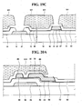
- FIG. 17A is a cross-sectional view taken along line A-A' of FIG. 16.
- FIG. 17B is a cross-sectional view taken along line B-B' of FIG. 16.
- FIG. 17C is a cross-sectional view taken along line C-C' of FIG. 16.
- FIGS. 18A, 19A, 20A, and 21A are cross-sectional views showing processing steps of the method of fabricating the TFT array substrate cross-sectional view shown in FIG. 17A according to a fifth exemplary embodiment of the present invention.
- FIGS. 18B, 19B, 20B, and 21B are cross-sectional views showing processing steps of the method of fabricating the TFT array substrate cross-sectional view shown in FIG. 17B according to the fifth exemplary embodiment of the present invention.
- FIGS. 18C, 19C, 20C, and 21C are cross-sectional views showing processing steps of the method of fabricating the TFT array substrate cross-sectional view shown in FIG. 17C according to the fifth exemplary embodiment of the present invention.
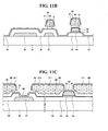
- FIGS. 22A and 23A are cross-sectional views showing processing steps of the method of fabricating the TFT array substrate cross-sectional view shown in FIG. 17A according to a sixth exemplary embodiment of the present invention.
- FIGS. 22B and 23B are cross-sectional views showing processing steps of the method of fabricating the TFT array substrate cross-sectional view shown in FIG. 17B according to the sixth exemplary embodiment of the present invention.
- FIGS. 22C and 23C are cross-sectional views showing processing steps of the method of fabricating the TFT array substrate cross-sectional view shown in FIG. 17C according to the sixth exemplary embodiment of the present invention.
- FIG. 1 is a layout of a TFT array substrate according to a first embodiment of the present invention
- FIG. 2A, FIG. 2B, and FIG. 2C are cross-sectional views taken along lines A-A', B-B', and C-C', respectively, of FIG. 1.
- a TFT array substrate includes a TFT arranged on an insulating substrate, a first passivation film covering the TFT, and a second passivation film arranged on the first passivation film.
- the TFT is a three-terminal device including a control terminal, an input terminal, and an output terminal and may include a gate electrode, a source electrode, a drain electrode, and a semiconductor layer.
- the gate electrode may be the control terminal
- the source electrode may be the input terminal
- the drain electrode may be the output terminal.
- the semiconductor layer may form a channel region of the TFT.
- an insulating substrate 10 supports a TFT and may be formed of, for example, transparent glass or plastic.
- a gate line 22, a gate pad 27, and a gate electrode 24 are arranged on the insulating substrate 10.
- Plural gate lines 22 for gate signal transmission are disposed on the insulating substrate 10.
- the gate lines 22 are spaced apart from each other and extend parallel with each other in a first direction, such as a transverse direction shown in FIG. 1.
- a gate pad 27 having an expanded width is connected to an end of each gate line 22.
- the gate pad 27 may be arranged at two opposite terminals of the gate line 22, or may not be formed.
- the gate electrode 24 is connected to the gate line 22.
- Plural gate electrodes 24 may also be connected to the gate line 22. Each gate electrode 24 may extend out from the gate line 22.
- the gate electrode 24, the gate line 22, and the gate pad 27 may be arranged directly on the insulating substrate 10. Throughout this specification, the gate electrode 24, the gate line 22, and the gate pad 27 may be collectively referred to as a gate interconnection line for the convenience of explanation.
- the storage electrode 28 which may be formed of the same material as the gate interconnection line, may be arranged directly on the insulating substrate 10.
- the storage electrode 28 is arranged in the vicinity of the gate line 22 and extends in the first direction parallel to the gate line 22.
- a storage electrode pad (not shown), which may be similar to the gate pad 27, may be arranged on at least a terminal of the storage electrode 28.
- the shape of the storage electrode 28 may vary but the invention is not limited to the shape shown in Fig. 1.
- the gate interconnection line and the storage electrode 28 may be formed as a single layer and may be formed of aluminum (Al), copper (Cu), silver (Ag), molybdenum (Mo), chrome (Cr), titanium (Ti), tantalum (Ta), or alloys thereof, or as a multi-layered structure including combinations of these materials, but the invention is not limited thereto.
- the gate insulation layer 30 may be formed of silicon nitride (SiNx) and may be arranged on the gate interconnection line and the storage electrode 28. However, the gate insulation layer 30 may not be arranged on the gate interconnection line in a gate contact portion 76 where the gate pad 27 contacts an auxiliary gate pad 96. The gate insulation layer 30 overlaps with the gate interconnection line and the insulating substrate 10 in an area where a data interconnection line, to be described below, is arranged. The gate insulation layer 30 may expose the insulating substrate 10 in a pixel area where a pixel electrode 92 is arranged.
- a semiconductor layer 44 and ohmic contact layers 52, 55 and 56 which may be formed of silicide or n+ hydrogenated amorphous silicon doped with n-type impurities at high concentration, are arranged on the gate insulating layer 30.
- the semiconductor layer 44 is arranged in substantially the same pattern as the data interconnection line, to be described in further detail below, except for the channel region.
- a channel region of a thin film transistor corresponds to where the semiconductor layer 44 overlaps with the gate electrode 24.
- the ohmic contact layers 52, 55 and 56 are arranged in substantially the same pattern as the overlying data interconnection line, to be described in further detail below.
- the ohmic contact layers 52, 55 and 56 do not contact each other in a region corresponding to the channel region.
- the data line 62, the data pad 67, the source electrode 65, and the drain electrode 66 are arranged on the semiconductor layer 44 and on the ohmic contact layers 52, 55 and 56.
- Plural data lines 62 are disposed on the ohmic contact layers 52.
- the data lines 62 are spaced apart from each other and extend parallel with each other in a second direction, such as a longitudinal direction shown in FIG. 1.
- the data lines 62 cross with the gate lines 22.
- a data pad 67 having an expanded width is connected to an end of each data line 62.
- the data pad 67 may be arranged at two opposite terminals of the data line 62, or may not be formed.
- the source electrode 65 is connected to the data line 62. Plural source electrodes 65 may also be connected to each data line 62. Each source electrode 62 is opposite to and faces a drain electrode 66. The semiconductor layer 44 may be exposed between the source electrode 65 and the drain electrode 66.
- the data line 62, the data pad 67, the source electrode 62, and the drain electrode 66 may be collectively referred to as a data interconnection line for the convenience of explanation.
- the data interconnection line may be formed as a single layer of Al, Cu, Ag, Mo, Cr, Ti, Ta, or alloys thereof, or as a multi-layered structure including combinations of these materials, but the invention is not limited thereto.
- a first passivation film 72 is arranged on the data interconnection line except in an area where the drain electrode 66 contacts the pixel electrode 92, referred to as a drain electrode-pixel electrode contact portion 101, and except in an area where the data pad 67 contacts an auxiliary data pad 97, referred to as a data contact portion 77.
- the first passivation film 72 is also arranged on the channel region of the exposed semiconductor layer 44.
- the first passivation film 72 is arranged on the gate interconnection line except for the gate contact portion 76. Specifically, in an area where the gate interconnection line does not overlap with the data interconnection line, the first passivation film 72 is arranged on the gate insulating layer 30 in a region corresponding to the gate interconnection line.
- the first passivation film 72 is arranged on the corresponding data interconnection line.
- An area where the gate interconnection line overlaps with the data interconnection line may include an area where the gate line 22 and the data line 62 intersect with each other, and in an area where the source electrode 65 and the drain electrode 66 overlap with the gate electrode 24.
- the first passivation film 72 is arranged on the semiconductor layer 44. Referring to FIG. 2B, the first passivation film 72 is not positioned on the storage electrode 28. However, the invention is not limited thereto and the first passivation film 72 may be positioned on the storage electrode 28 in another exemplary embodiment of the invention.
- the first passivation film 72 may be formed of silicon oxide (SiO 2 ) or silicon oxynitride (SiO x N y ).
- the first passivation film 72 may have a thickness in a range of about 50 ⁇ to about 500 ⁇ , or in a range of about 100 ⁇ to about 300 ⁇ .
- a second passivation film 82 is arranged on the first passivation film 72.
- the second passivation film 82 may overlap with the first passivation film 72. More specifically, the second passivation film 82 is arranged on the first passivation film 72 throughout the entire area of the TFT array substrate but does not entirely cover the first passivation film 72. In other words, the outer sidewall of the second passivation film 82 is positioned inside the outer sidewall of the first passivation film 72. The sidewall of the first passivation film 72 extends beyond the sidewall of the second passivation film 82. In another exemplary embodiment of the invention, where the first passivation film 72 is positioned on the storage electrode 28, the second passivation film 82 may or may not be positioned on the storage electrode 28.
- the gate insulating layer 30 is patterned to expose the insulating layer 10 of the pixel area.
- the gate insulating layer 30 extend beyond the second passivation film 82, and the outer sidewalls of the first passivation film 72 may be exposed by the second passivation film 82.
- the outer sidewall of the first passivation film 72 may be aligned with the outer sidewalls of the gate insulating layer 30.
- the outer sidewalls of the first passivation film 72 may extend beyond to be positioned outside the outer sidewalls of the the gate insulating layer 30.
- the second passivation film 82 may be formed of silicon nitride (SiN).
- the second passivation film 82 may be thicker than the first passivation film 72.
- the second passivation film 82 may have a thickness in a range of about 1,000 ⁇ to about 3,000 ⁇ , or in a range of about 1,500 ⁇ to about 2,500 ⁇ .
- the first passivation film 72 and the second passivation film 82 may protect lower structures such as the data interconnection line, the semiconductor layer 44, and the gate interconnection line.
- the gate contact portion 76 is formed through the gate insulating layer 30, the first passivation film 72 and the second passivation film 82.
- the data contact portion 77 is formed through the first passivation film 72 and the second passivation film 82.
- the pixel electrode 92 may be made of a transparent conductive material such as indium tin oxide (ITO) or indium zinc oxide (IZO), or a material having superior reflectivity such as copper (Cu) or silver (Ag) may be arranged on the exposed insulating substrate 10 in the pixel area.
- the pixel electrode 92 extends to the drain electrode-pixel electrode contact portion 101 and is connected to the drain electrode 66 at the drain electrode-pixel electrode contact portion 101.
- the first passivation film 72 and the second passivation film 82 do not overlap with the pixel electrode 92.
- the pixel electrode 92 overlaps with the gate insulating layer 30.
- the pixel electrode 92 may overlap with the first passivation film 72 and/or the second passivation film 82 in an area of the storage electrode 28 when the first passivation film 72 and/or the second passivation film 82 are arranged on the storage electrode 28.
- the gate insulating layer 30, the first passivation film 72, and the second passivation film 82, which are interposed between the storage electrode 28 and the pixel electrode 92, may have a uniform thickness to increase a driving margin.
- the auxiliary gate pad 96 connected to the gate pad 27 is arranged in the formation area of the gate pad 27, and the auxiliary data pad 97 connected to the data pad 67 is arranged in the formation area of the data pad 67.
- the auxiliary gate pad 96 and the auxiliary data pad 97 may be formed of the same material, which may be the same material used to form the pixel electrode 92. ,
- FIGS. 3A, 4A, 5A, 6A, 7A, 8A, 9A, 10A, and 11A are cross-sectional views showing processing steps of the method of fabricating the TFT array substrate cross-sectional view shown in FIG. 2A according to a second exemplary embodiment of the present invention.
- FIGS. 3B, 4B, 5B, 6B, 7B, 8B, 9B, 10B, and 11B are cross-sectional views showing processing steps of the method of fabricating the TFT array substrate cross-sectional view shown in FIG. 2B according to the second exemplary embodiment of the present invention.
- 3C, 4C, 5C, 6C, 7C, 8C, 9C, 10C, and 11C are cross-sectional views showing processing steps of the method of fabricating the TFT array substrate cross-sectional view shown in FIG. 2C according to the second exemplary embodiment of the present invention.
- the gate interconnection line and the storage electrode 28 are formed on the insulating substrate 10. More specifically, a gate conductive layer is deposited on the insulating substrate 10 using, for example, sputtering, and is then photo-etched, thereby forming the gate line 22, the gate pad 27, the gate electrode 24, and the storage electrode 28.
- a gate insulating layer 30, a first amorphous silicon layer 40, which may be made of hydrogenated amorphous silicon, and a second amorphous silicon layer 50, which may be made of silicide or n+ hydrogenated amorphous silicon doped with high concentration n-type impurities, are deposited on the insulating substrate 10.
- the gate insulating layer 30, the first amorphous silicon layer 40, and the second amorphous silicon layer 50 may be deposited using, for example, chemical vapor deposition (CVD).
- a data conductive layer 60 is deposited on the second amorphous silicon layer 50 using, for example, sputtering.
- a photoresist pattern 201 and 202 is formed on the data conductive layer 60.
- the photoresist pattern includes a first region 201 and a second region 202 having a smaller thickness than the first region 201.
- the first region 201 covers a formation area of a data line 62, a data pad 67, a source electrode 65, and a drain electrode 66 shown in FIG. 2A, FIG. 2B, and FIG. 2C.
- the second region 202 covers a space between the source electrode 65 and the drain electrode 66.
- the size of the photoresist pattern 201 and 202 for each region is selected with the consideration that it may be reduced in sized during subsequent etching and ashing processes.
- the photoresist pattern having different thicknesses for different regions may be formed using a slit mask or a half-tone mask, which can also be applied to other photoresist patterns to be described below.
- the exposed data conductive layer 60 is etched using the photoresist pattern 201 and 202 shown in FIG. 5A, FIG. 5B, and FIG. 5C as an etching mask.
- the data conductive layer 60 may be etched using one of various methods depending on the required type and thickness of the data conductive layer 60, but may be etched using wet etching.
- patterns of the data line 62 and the data pad 67 are formed.
- patterns of the source electrode 65 and the drain electrode 66 are not yet formed and the data conductive layer 64 remains integrated in the channel region.
- the second amorphous silicon layer 50 is exposed and the exposed second amorphous silicon layer 50 and the first amorphous silicon layer 40 thereunder are etched.
- the second amorphous silicon layer 50 and the first amorphous silicon layer 40 may be etched using, for example, dry etching.
- a semiconductor layer 44 is formed.
- the gate insulating layer 30 may be exposed.
- the photoresist pattern used as an etching mask is partially etched and thus is reduced in size. Patterns 52 and 54 of the etched second amorphous silicon layer and the completed semiconductor layer 44 are substantially the same as those of the data line 62, the data pad 67, and the data conductive layer 64 that is not separated in the channel region.
- the data conductive layer 64 is exposed by removing the second region 202 of the photoresist pattern.
- the second region 202 may be removed by an ashing process using O 2 .
- the first region 211 is also reduced in size.
- the second region 211 may be removed, and in this case, the ashing process may be skipped.
- a region of the exposed data conductive layer 64 corresponding to the channel region is etched using the first region 211 of the down-sized photoresist pattern as an etching mask.
- patterns of the source electrode 65 and the drain electrode 66 are formed and the second amorphous silicon layer 54 is exposed through the space between the source electrode 65 and the drain electrode 66.
- the exposed second amorphous silicon layer 54 is etched to be separated.
- ohmic contact layers 52, 55, and 56 are formed.
- the semiconductor layer 44 is exposed in an area where the second amorphous silicon layer 54 is etched.
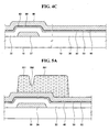
- a first insulating layer 70 and a second insulating layer 80 are sequentially deposited on the TFT array substrate obtained by performing the processing steps illustrated in FIG. 8A, FIG. 8B, and FIG. 8C using, for example, CVD.
- a photoresist pattern 301 and 302 is formed on the second insulating layer 80.
- the photoresist pattern includes a first region 301 and a second region 302 having a smaller thickness than the first region 301.
- the first region 301 covers a formation area of the gate interconnection line, a formation area of a data interconnection line, and a formation area of the semiconductor layer 44.
- the second insulating layer 80 remains exposed in a formation area of a drain electrode-pixel electrode contact portion 101, an area of the gate pad 27, and an area of the data pad 67.
- the second region 302 covers a formation area of the storage electrode 28.
- the exposed second insulating layer 80 and the first insulating layer 70 thereunder are etched using the photoresist pattern 301 as an etching mask to form the second passivation film 82 and the first passivation film 72.
- the second insulating layer 80 and the first insulating layer 70 may be etched using, for example, dry etching.
- the etching may be anisotropic etching or isotropic etching. In order to secure a lift-off margin due to an undercut, isotropic etching may be used.
- An etching gas to etch the second insulating layer 80 and the first insulating layer 70 may be selected such that the second insulating layer 80 has a large etching selectivity with respect to the first insulating layer 70. More specifically, the selected etching gas may possess a higher etching rate with respect to the second insulating layer 80 than with respect to the first insulating layer 70. For example, an etching gas may be used that provides a 1:5 - 1:20 ratio of an etching rate with respect to the first insulating layer 70 to an etching rate with respect to the second insulating layer 80.
- etching gas O 2 , CF 4 , SF 6 , CHF 3 , O 2 , or combinations thereof may be used as an etching gas, and the etching rate can be controlled by adjusting the combination of constituents of the etching gas used or the composition ratio of the combination.
- a non-limiting example of the etching gas may include an etching gas of SF 6 and O 2 mixed in a ratio of 2:1.
- the time required to etch the first insulating layer 70 increases after etching the second insulating layer 80.
- the second insulating layer 80 can be sufficiently over-etched under the inner side of the photoresist pattern 301, thereby securing an undercut having a sufficiently large width.
- structures such as the data pad 67 and the drain electrode 66 may be protected from etching by being covered with the first insulating layer 70.
- a material susceptible to dry etching such as molybdenum
- the semiconductor layer 44 is protected by the first insulating layer 70 during over-etching of the second passivation film 82, thereby preventing undercut of the semiconductor layer 44.
- the first insulating layer 70 Since the first insulating layer 70 has a low etching rate, it is patterned along the mask of the photoresist pattern 301 and 302, generating only a small amount of undercut. Thus, after etching the first insulating layer 70 to form the first passivation film 72, a sidewall of the first passivation film 72 extends beyond a sidewall of the second passivation film 82.
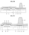
- the gate insulating layer 30 under the first passivation film 72 is etched.
- the second passivation film 82 is over-etched to the inside of the gate insulating layer 30 and the width of the undercut increases.
- the width of the undercut formed by the second passivation film 82 may be about 4 ⁇ m to about 30 ⁇ m.
- the etching rate of the gate insulating layer 30 may be larger than the etching rate of the first passivation film 72.
- an undercut formed in the gate insulating layer 30 may be formed under the first passivation film 72 due to this etching rate difference.
- the extent to which the gate insulating layer 30 is etched may be small.
- the degree of protrusion of the first passivation film 72 with respect to the second passivation film 82 is larger than that of the first passivation film 72 with respect to the gate insulating layer 30.
- the outer sidewall of the second passivation film 82 is positioned inside the outer sidewall of the gate insulating layer 30.
- the relationship between positions of the gate insulating layer 30 and the first passivation film 72 may vary according to processing conditions.
- the degree of protrusion of the first passivation film 72 with respect to the gate insulating layer 30 can be minimized or the sidewalls of the first passivation film 72 and the gate insulating layer 30 can be aligned with each other.
- the outer sidewall of the first passivation film 72 may be positioned inside the outer sidewall of the gate insulating layer 30.
- the drain electrode 66 is exposed and the insulating substrate 10 in a pixel region is also exposed.
- the gate pad 27 and the data pad 67 are also exposed, thereby forming a gate contact portion 76 and the data contact portion 77, respectively.
- the photoresist pattern 301 and 302 may be reduced in size during etching of the second insulating layer 80, the first insulating layer 70, and the gate insulating layer 30, which are not covered by the photoresist pattern 301 and 302.
- the second region 302 of the photoresist pattern can be removed and only a region 311 having a reduced size can remain after the etching step, as shown in Fig. 10A, FIG. 10B, and FIG. 10C.
- the remaining insulating layers 30, 70, and 80 under the second region 302 can be adjusted according to the thickness of the second region 302 of the photoresist pattern and/or the etching rate with respect to the photoresist pattern 301 and 302.
- the thickness of the second region 302 may be a second thickness larger than the first thickness or an etching gas providing a second etching rate with respect to the photoresist pattern 301 and 302 that is higher than the first etching rate may be used.
- the second insulating layer 80 may be removed and layers under the first insulating layer 70 may remain.
- the thickness of the second region 302 may be a third thickness that is larger than the second thickness or an etching gas providing a third etching rate with respect to the photoresist pattern 301 and 302 that is higher than the second etching rate may be used.
- an etching gas providing a third etching rate with respect to the photoresist pattern 301 and 302 that is higher than the second etching rate may be used.
- the gate insulating layer 30 among insulating layers under the second region 302 may remain. Since the duration of the etching process may increase, during which time the gate insulating layer 30 is protected by the first insulating layer 70, non-uniform etching of the gate insulating layer 30 can be prevented. Thus, uniform storage capacity may be achieved and a driving margin may be increased. Similarly, when the gate insulating layer 30 and the first insulating layer 70 remain on the storage electrode 28, uniform storage capacity can be achieved by preventing non-uniform etching.
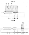
- a pixel electrode conductive material 90 is deposited on the entire surface of the insulating substrate 10 using, for example, sputtering. A portion of the pixel electrode conductive material 90 is deposited on the photoresist, pattern 311 and the remaining pixel electrode conductive material 90 is deposited on the exposed structure.
- the photoresist pattern 311 and the pixel electrode conductive material 90 thereon may be removed using a lift-off process. More specifically, if a photoresist stripper including an amine group and a glycol group contacts the photoresist pattern 311 by spraying or dipping, it may exfoliate the photoresist pattern 311 from the second passivation film 82 by dissolving the photoresist pattern 311 and may remove the pixel electrode conductive material 90 on the photoresist pattern 311.
- a removal rate of the photoresist pattern 311 and the pixel electrode conductive material 90 thereon is dependant on the contact time and contact area of the photoresist stripper on the photoresist pattern 311.
- a contact area between the first region 311 of the photoresist pattern and the photoresist stripper increases. Therefore, it can be easily understood that the removal rate of the photoresist stripper with respect to the photoresist pattern 311 and the pixel electrode conductive material 90 thereon is improved.
- patterns of a pixel electrode 92, an auxiliary gate pad 96, and an auxiliary data pad 97 are formed.
- FIGS. 12A, 13A, 14A, and 15A are cross-sectional views showing processing steps of the method of fabricating the TFT array substrate cross-sectional view shown in FIG. 2A according to a third exemplary embodiment of the present invention.
- FIGS. 12B, 13B, 14B, and 15B are cross-sectional views showing processing steps of the method of fabricating the TFT array substrate cross-sectional view shown in FIG. 2B according to the third exemplary embodiment of the present invention.
- FIGS. 12C, 13C, 14C, and 15C are cross-sectional views showing processing steps of the method of fabricating the TFT array substrate cross-sectional view shown in FIG. 2C according to the third exemplary embodiment of the present invention.
- the method according to the third exemplary embodiment of the present invention includes the same steps of forming patterns of the source electrode 65 and the drain electrode 66, and the ohmic contact layers 52, 55, and 56, and exposing the semiconductor layer 44 as in the method according to the second exemplary embodiment of the present invention.
- the first insulating layer 70 and the second insulating layer 80 are sequentially deposited on the structure resulting from performing these steps.
- a photoresist pattern 401 and 402 is formed on the second insulating layer 80.
- the photoresist pattern includes a first region 401, and a second region 402 having a smaller thickness than the second region 402.
- the first region 401 covers a gate interconnection line, a formation area of a data interconnection line, and a formation area of the semiconductor layer 44.
- the second insulating layer 80 in a formation area of the gate pad 27 is exposed as in the second exemplary embodiment of the present invention.
- a formation area of a drain electrode-pixel electrode contact portion 101 and an area of the data pad 67 are covered with the second region 402 unlike in the second exemplary embodiment of the present invention.
- the thickness of the second region 402 according to the third exemplary embodiment of the present invention may be larger than that of the second region 202 according to the second exemplary embodiment of the present invention.
- the exposed second insulating layer 80, the first insulating layer 70 thereunder, and the gate insulating layer 30 are sequentially primarily etched using the photoresist pattern as an etching mask.
- the etching may be substantially similar as that of the second insulating layer 80, the first insulating layer 70, and the gate insulating layer 30 according to the second exemplary embodiment of the present invention.
- the first passivation film 72 and the gate insulating layer 30 may extend beyond the second passivation film 82, and the outer sidewalls of the first passivation film 72 may be positioned inside the outer sidewalls of the gate insulating layer 30, may be aligned with the outer sidewalls of the gate insulating layer 30, or may be positioned on the outer sidewalls of the gate insulating layer 30.
- a formation area of the drain electrode-pixel electrode contact portion 101 and the data pad 67 are protected by the second region 402 of the photoresist pattern, damage to the drain electrode 66 and the data pad 67 can be further prevented.
- the semiconductor layer 44 may be protected by the second passivation film 82, thereby preventing undercut of the semiconductor layer 44.
- the photoresist pattern 401 and 402 used as an etching mask may be partially etched and thus reduced in size.
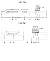
- the second region 402 of the photoresist pattern is removed to expose the drain electrode-pixel electrode contact portion 101, the data pad 67, and the second passivation film 82 on the storage electrode 28.
- the second region 402 may be removed by an ashing process using O 2 .
- the photoresist pattern 411 may be reduced in size.
- the second region 402 of the photoresist pattern may have been removed during the primary etching, in which case the ashing process may be skipped.
- the second passivation film 82 and the first passivation film 72 in the drain electrode-pixel electrode contact portion 101, a formation area of the data pad 67, and a formation area of the storage electrode 28 may be secondarily etched using the first region 411 of the down-sized photoresist pattern.
- the drain electrode 66 on the drain electrode-pixel electrode contact portion 101, the data pad 67, and the gate insulating layer 30 on the storage electrode 28 are exposed. Since the etching rate of the first insulating layer 70 is lower than that of the second insulating layer 80, the width of the undercut of the second passivation film 82 further increases during the secondary etching.
- the gate insulating layer 30 is not etched and only the drain electrode-pixel electrode contact portion 101, and the second insulating layer 80 and the first insulating layer 70 in a formation area of the storage electrode 28 are etched, which may be referred to as partial-surface etching.
- the primary etching may be performed for about 30 to about 200 seconds, but the secondary etching may be performed for about 10 to about 20 seconds.
- the gate insulating layer 30 on the storage electrode 28 may be prevented from being damaged by an etching gas, thereby providing uniformity of the thickness of the gate insulating layer 30 and thus increasing a driving margin. Furthermore, the time during which the semiconductor layer 44 is exposed to the etching gas may be small, thereby preventing undercut.
- the photoresist pattern may cover the area where the gate pad 27 is formed.
- a portion of the photoresist pattern covering the area where the gate pad 27 is formed may be a third region (not shown) having a smaller thickness than the second region 402.
- the third region thickness may be such that it is entirely removed and the second insulating layer 80, the first insulating layer 70, and/or the gate insulating layer 30 under the third region are partially removed during the primary etching.
- the gate insulating layer 30 covering the gate pad 27 may be entirely removed during the secondary etching.
- the second region 402 of the photoresist pattern covering the drain electrode-pixel electrode contact portion 101 and/or the area where the data pad 67 is formed may be partially or entirely omitted.
- the methods of fabricating the TFT array substrate according to the second exemplary embodiment and the third exemplary embodiment of the present invention are different in that etching of the first passivation film and etching of the second passivation film are performed simultaneously or separately, but the methods may be partially combined with each other.
- the drain electrode-pixel electrode contact portion 101 and/or the area where the data pad 67 is formed according to the current embodiment of the present invention may be covered with the second region 402 of the photoresist pattern.
- the second region 402 of the photoresist pattern and the second passivation film and the first passivation film under the second region may be entirely removed during etching of the second passivation film, the first passivation film, and the gate insulating layer in an exposed region.
- such a combination is only an example.
- FIG. 16 is a layout of a TFT array substrate according to a fourth exemplary embodiment of the present invention and FIG. 17A, FIG. 17B, and FIG. 17C are cross-sectional views taken along lines A-A', B-B', and C-C', respectively, of FIG. 16.
- the TFT array substrate according to the fourth exemplary embodiment of the present invention is different from that according to the first exemplary embodiment of the present invention in that a gate insulating layer 30 is arranged on an entire surface of the insulating substrate 10 except for a peripheral area of a gate line 22, a peripheral area of the data line 62, and the gate contact portion 76. According to a manufacturing process, the peripheral area of the gate line 22 and the peripheral area of the data line 62 may not be separated.
- a pixel electrode 92 overlaps with the gate insulating layer 30, the first passivation film 72, and the second passivation film 82 and is positioned on the second passivation film 82.
- the first passivation film 72 and the second passivation film 82 as well as the gate insulating layer 30 are interposed between the pixel electrode 92 and the storage electrode 28.
- the first passivation film 72 and the second passivation film 82 cover most of a formation area of the gate insulating layer 30 except for a formation area of the data contact portion 77 where the data pad 67 contacts the auxiliary data pad 97,and the drain electrode-pixel electrode contact portion 101. However, in a formation area of the gate line 22 and the data line 62, the gate line 22 and the data line 62 are separated to separate the pixel electrode 92 for each pixel.
- the drain electrode-pixel electrode contact portion 101 is surrounded by the first passivation film 72 and the second passivation film 82. In the current exemplary embodiment of the present invention, the first passivation film 72 is entirely overlapped by the second passivation film 82.
- the pixel electrode 92 is arranged on the gate insulating layer 30, the first passivation film 72, and the second passivation film 82 in the TFT array substrate according to the current exemplary embodiment of the present invention, a step between a formation area of the pixel electrode 92 and a formation area of the TFT is reduced.
- the uniformity of a cell gap can be improved.
- FIGS. 18A, 19A, 20A, and 21A are cross-sectional views showing processing steps of the method of fabricating the TFT array substrate cross-sectional view shown in FIG. 17A according to a fifth exemplary embodiment of the present invention.
- FIGS. 18B, 19B, 20B, and 21B are cross-sectional views showing processing steps of the method of fabricating the TFT array substrate cross-sectional view shown in FIG. 17B according to the fifth exemplary embodiment of the present invention.
- FIGS. 18C, 19C, 20C, and 21C are cross-sectional views showing processing steps of the method of fabricating the TFT array substrate cross-sectional view shown in FIG. 17C according to the fifth exemplary embodiment of the present invention.
- the method according to the current exemplary embodiment of the present invention includes substantially the same steps of forming patterns of the source electrode 65 and the drain electrode 66, and ohmic contact layers 52, 55, and 56, and exposing the semiconductor layer 44 as in the second exemplary embodiment of the present invention.
- the first insulating layer 70 and the second insulating layer 80 are sequentially deposited on the structure resulting from performing the above steps.
- the photoresist pattern 501 and 502 is formed on the second insulating layer 80.
- the photoresist pattern includes a first region 501, and a second region 502 having a smaller thickness than the first region 501.
- the first region 501 covers a formation area of the gate interconnection line, a formation area of the data interconnection line, and a formation area of the semiconductor layer 44.
- a formation area of the gate pad 27, a formation area of the data pad 67, and the second insulating layer 80 of the drain electrode-pixel electrode contact portion 101 are exposed.
- the second region 502 covers most of the pixel region as well as a formation area of the storage electrode 28, but a peripheral area of the gate line 22 and a peripheral area of the data line 62 are exposed.
- the exposed second insulating layer 80, the first insulating layer 70, and the gate insulating layer 30 are etched using the photoresist pattern 501 and 502 as an etching mask to form the second passivation film 82 and the first passivation film 72.
- the drain electrode 66 of the drain electrode-pixel electrode contact portion 101 is exposed and the insulating substrate 10 in the peripheral area of the gate line 22 and the peripheral area of the data line 62 is exposed.
- the gate pad 27 and the data pad 67 are exposed and thus the gate contact portion 76 and the data contact portion 77 are formed.
- etching of the second insulating layer 80 and the first insulating layer 70 is performed using an etching gas having a higher etching rate with respect to the second insulating layer 80 than the first insulating layer 70 as in the second exemplary embodiment.
- the second passivation film 82 under the photoresist pattern 501 and 502 may be etched to include an undercut having a sufficiently large width.
- the second region 502 of the photoresist pattern is removed.
- the second region 502 may be removed by an ashing process using O 2 .
- the photoresist pattern 511 may be reduced in size.
- the second passivation film 82 of the pixel region is exposed.
- the second region 502 of the photoresist pattern may have been removed during etching of the second insulating layer 80 and the first insulating layer 70 thereunder, in which case the ashing process may be skipped.
- the pixel electrode conductive material 90 is deposited on the insulating substrate 10.
- the photoresist pattern 511 and the pixel electrode conductive material 90 above the photoresist pattern 511 are removed. This step may be performed in a substantially similar manner as the lift-off process described in the second exemplary embodiment of the present invention. As a result, as shown in FIG. 17A, FIG. 17B, and FIG. 17C, patterns of the pixel electrode 92, the auxiliary gate pad 96, and the auxiliary data pad 97 are formed.
- FIGS. 22A and 23A are cross-sectional views showing processing steps of the method of fabricating the TFT array substrate cross-sectional view shown in FIG. 17A according to a sixth exemplary embodiment of the present invention.
- FIGS. 22B and 23B are cross-sectional views showing processing steps of the method of fabricating the TFT array substrate cross-sectional view shown in FIG. 17B according to the sixth exemplary embodiment of the present invention.
- FIGS. 22C and 23C are cross-sectional views showing processing steps of the method of fabricating the TFT array substrate cross-sectional view shown in FIG. 17C according to the sixth exemplary embodiment of the present invention.
- the method according to the sixth exemplary embodiment of the present invention includes substantially similar steps of forming patterns of the source electrode 65 and the drain electrode 66, and the ohmic contact layers 52, 55, and 56, and exposing the semiconductor layer 44 as those in the second exemplary embodiment of the present invention.
- the first insulating layer 70 and the second insulating layer 80 are sequentially deposited on the structure resulting from performing the steps.
- the photoresist pattern 601 is formed on the second insulating layer 80.
- the photoresist pattern 601 is substantially similar as the photoresist pattern shown in previous exemplary embodiments except that photoresist pattern 601 has a uniform thickness without being separated into a first region and a second region.
- the exposed second insulating layer 80, the first insulating layer 70 thereunder, and the gate insulating layer 30 thereunder are etched using the photoresist pattern 601 as an etching mask to form the second passivation film 82 and the first passivation film 72.
- the drain electrode 66 of the drain electrode-pixel electrode contact portion 101 is exposed, and the insulating substrate 10 in the peripheral area of the gate line 22 and the peripheral area of the data line 62 is exposed.
- the gate pad 27 and the data pad 67 are also exposed and thus the gate contact portion 76 and the data contact portion 77 are formed.
- the drain electrode 66 and the data pad 67 under the first insulating layer 70 are protected from an etching gas until the first insulating layer 70 is etched and removed.
- the time during which the drain electrode 66 and the data pad 67 under the first insulating layer 70 are exposed to the etching gas is reduced, thereby preventing damage to the drain electrode 66 and the data pad 67 under the first insulating layer 70.
- the photoresist pattern 601 is removed and the pixel electrode conductive material is deposited and is patterned using a photolithography process, thereby completing the pixel electrode 92, the auxiliary gate pad 96, and the auxiliary data pad 97 as shown in FIG. 17A, FIG. 17B, and FIG. 17C. Since the current exemplary embodiment of the present invention includes a photolithography process for a pixel electrode conductive material, it is not necessary to remove the second passivation film 82, the first passivation film 72, and the gate insulating layer 30 in the peripheral areas of the gate line 22 and the data line 62.
- the present invention is not limited thereto.
- the semiconductor layer and the ohmic contact layer may be formed only in the channel region.
- a photoresist pattern for forming the semiconductor layer and the ohmic contact layer and a photoresist pattern for forming the data interconnection line may be formed using separate masks unlike in the embodiments of the present invention. Since such a TFT array substrate and a method of fabricating the same are well known to those skilled in the art and a difference in subsequent processes can be easily understood by those skilled in the art, they will not be further described herein.
- an undercut having a sufficiently large width may be provided under the photoresist pattern, thereby providing a superior lift-off margin.
- the uniform thickness of the insulating layer interposed between the storage electrode and the pixel electrode may increase a driving margin.
- the drain electrode and the data pad may be prevented from being damaged, thereby securing a sufficiently large contact area between conductive materials in the contact portion.
Landscapes
- Physics & Mathematics (AREA)
- Nonlinear Science (AREA)
- Mathematical Physics (AREA)
- Chemical & Material Sciences (AREA)
- Crystallography & Structural Chemistry (AREA)
- General Physics & Mathematics (AREA)
- Optics & Photonics (AREA)
- Engineering & Computer Science (AREA)
- Microelectronics & Electronic Packaging (AREA)
- Thin Film Transistor (AREA)
- Liquid Crystal (AREA)
- Devices For Indicating Variable Information By Combining Individual Elements (AREA)
Applications Claiming Priority (1)
| Application Number | Priority Date | Filing Date | Title |
|---|---|---|---|
| KR1020060060246A KR101201972B1 (ko) | 2006-06-30 | 2006-06-30 | 박막 트랜지스터 어레이 기판 및 이의 제조 방법 |
Publications (1)
| Publication Number | Publication Date |
|---|---|
| EP1873833A1 true EP1873833A1 (en) | 2008-01-02 |
Family
ID=38473917
Family Applications (1)
| Application Number | Title | Priority Date | Filing Date |
|---|---|---|---|
| EP07011733A Withdrawn EP1873833A1 (en) | 2006-06-30 | 2007-06-15 | Thin film transistor array substrate and method of fabricating the same |
Country Status (6)
Families Citing this family (19)
| Publication number | Priority date | Publication date | Assignee | Title |
|---|---|---|---|---|
| KR20070019457A (ko) * | 2005-08-12 | 2007-02-15 | 삼성전자주식회사 | 박막 트랜지스터 표시판 및 이를 포함하는 액정표시장치 |
| JP5380037B2 (ja) * | 2007-10-23 | 2014-01-08 | 株式会社半導体エネルギー研究所 | 半導体装置の作製方法 |
| KR101048927B1 (ko) * | 2008-05-21 | 2011-07-12 | 엘지디스플레이 주식회사 | 액정표시장치 및 그 제조방법 |
| KR20100069935A (ko) * | 2008-12-17 | 2010-06-25 | 삼성전자주식회사 | 박막 트랜지스터 어레이 기판 및 이의 제조 방법 |
| KR101569766B1 (ko) * | 2009-01-29 | 2015-11-17 | 삼성디스플레이 주식회사 | 박막 트랜지스터 표시판 및 그 제조 방법 |
| TW201037436A (en) * | 2009-04-10 | 2010-10-16 | Au Optronics Corp | Pixel unit and fabricating method thereof |
| KR101648806B1 (ko) * | 2009-07-20 | 2016-08-31 | 삼성디스플레이 주식회사 | 박막 트랜지스터 표시판 및 그 제조 방법 |
| US20120133860A1 (en) * | 2009-08-04 | 2012-05-31 | Sharp Kabushiki Kaisha | Active matrix substrate, liquid crystal display panel, liquid crystal display device, and method for manufacturing active matrix substrate |
| WO2011016286A1 (ja) * | 2009-08-04 | 2011-02-10 | シャープ株式会社 | アクティブマトリックス基板、液晶表示パネル、液晶表示装置およびアクティブマトリックス基板の製造方法 |
| KR20120028050A (ko) * | 2010-09-14 | 2012-03-22 | 삼성전자주식회사 | 박막 트랜지스터 표시판의 제조 방법 |
| CN102637634B (zh) * | 2011-08-12 | 2014-02-26 | 北京京东方光电科技有限公司 | 一种阵列基板及其制作方法、显示装置 |
| KR101980765B1 (ko) | 2012-12-26 | 2019-08-28 | 엘지디스플레이 주식회사 | 에프에프에스 방식 액정표시장치용 어레이기판 및 그 제조방법 |
| KR102232539B1 (ko) * | 2013-11-13 | 2021-03-29 | 삼성디스플레이 주식회사 | 박막 트랜지스터, 이를 포함하는 표시 기판 및 박막 트랜지스터의 제조 방법 |
| CN104241296B (zh) * | 2014-08-21 | 2017-12-08 | 京东方科技集团股份有限公司 | 一种阵列基板及其制作方法和显示装置 |
| KR102411154B1 (ko) | 2015-07-09 | 2022-06-21 | 쑤저우 레킨 세미컨덕터 컴퍼니 리미티드 | 발광 소자 |
| CN108573928B (zh) | 2018-04-13 | 2020-12-29 | Tcl华星光电技术有限公司 | 一种tft阵列基板的制备方法及tft阵列基板、显示面板 |
| TWI878662B (zh) * | 2021-04-23 | 2025-04-01 | 元太科技工業股份有限公司 | 電子裝置 |
| CN114023699B (zh) * | 2021-10-29 | 2022-09-27 | 北海惠科光电技术有限公司 | 阵列基板的制备方法及其阵列基板 |
| TWI806796B (zh) * | 2022-11-01 | 2023-06-21 | 友達光電股份有限公司 | 薄膜電晶體 |
Citations (9)
| Publication number | Priority date | Publication date | Assignee | Title |
|---|---|---|---|---|
| US4575402A (en) * | 1985-02-13 | 1986-03-11 | Hewlett-Packard Company | Method for fabricating conductors in integrated circuits |
| EP0252179A1 (en) * | 1986-07-11 | 1988-01-13 | International Business Machines Corporation | Process for producing undercut mask profiles |
| DE19717363A1 (de) * | 1997-04-24 | 1998-10-29 | Siemens Ag | Herstellverfahren für eine Platinmetall-Struktur mittels Lift-off-Prozesses |
| WO2003075356A1 (en) * | 2002-03-07 | 2003-09-12 | Samsung Electronics Co., Ltd. | Contact portion of semiconductor device, and method for manufacturing the same, thin film transistor array panel for display device including the contact portion, and method for manufacturing the same |
| US20040129943A1 (en) * | 2002-12-31 | 2004-07-08 | Yoo Soon Sung | Thin film transistor array substrate and manufacturing method of the same |
| KR20060001165A (ko) * | 2004-06-30 | 2006-01-06 | 엘지.필립스 엘시디 주식회사 | 수평 전계 인가형 박막 트랜지스터 기판 및 그 제조 방법 |
| US20060024895A1 (en) * | 2004-07-27 | 2006-02-02 | Samsung Electronics Co., Ltd. | Thin film transistor array panel and manufacturing method thereof |
| US20060046365A1 (en) * | 2004-08-30 | 2006-03-02 | Hong-Sick Park | Method of manufacturing a thin film transistor substrate and stripping composition |
| US20060138428A1 (en) * | 2004-12-24 | 2006-06-29 | Ahn Byung C | Liquid crystal display device and fabricating method thereof, and thin film patterning method applied thereto |
Family Cites Families (8)
| Publication number | Priority date | Publication date | Assignee | Title |
|---|---|---|---|---|
| KR100223153B1 (ko) | 1996-05-23 | 1999-10-15 | 구자홍 | 액티브 매트릭스 액정표시장치의 제조방법 및 액티브매트릭스액정표시장치 |
| KR100720095B1 (ko) * | 2000-11-07 | 2007-05-18 | 삼성전자주식회사 | 박막 트랜지스터 어레이 기판 및 그 제조 방법 |
| US6693297B2 (en) | 2001-06-18 | 2004-02-17 | International Business Machines Corporation | Thin film transistor formed by an etching process with high anisotropy |
| KR100412619B1 (ko) * | 2001-12-27 | 2003-12-31 | 엘지.필립스 엘시디 주식회사 | 액정표시장치용 어레이 기판의 제조 방법 |
| US7317208B2 (en) * | 2002-03-07 | 2008-01-08 | Samsung Electronics Co., Ltd. | Semiconductor device with contact structure and manufacturing method thereof |
| TWI237395B (en) * | 2004-02-27 | 2005-08-01 | Au Optronics Corp | Method of fabricating thin film transistor array substrate and stacked thin film structure |
| KR101085136B1 (ko) * | 2004-12-04 | 2011-11-18 | 엘지디스플레이 주식회사 | 수평 전계 박막 트랜지스터 기판 및 그 제조 방법 |
| KR20070049740A (ko) * | 2005-11-09 | 2007-05-14 | 엘지.필립스 엘시디 주식회사 | 액정표시장치용 어레이기판과 그 제조방법 |
-
2006
- 2006-06-30 KR KR1020060060246A patent/KR101201972B1/ko active Active
-
2007
- 2007-06-01 US US11/756,855 patent/US20080042133A1/en not_active Abandoned
- 2007-06-15 EP EP07011733A patent/EP1873833A1/en not_active Withdrawn
- 2007-06-21 JP JP2007163971A patent/JP5395336B2/ja active Active
- 2007-06-27 TW TW096123307A patent/TW200827891A/zh unknown
- 2007-06-29 CN CN200710126331XA patent/CN101097928B/zh active Active
Patent Citations (9)
| Publication number | Priority date | Publication date | Assignee | Title |
|---|---|---|---|---|
| US4575402A (en) * | 1985-02-13 | 1986-03-11 | Hewlett-Packard Company | Method for fabricating conductors in integrated circuits |
| EP0252179A1 (en) * | 1986-07-11 | 1988-01-13 | International Business Machines Corporation | Process for producing undercut mask profiles |
| DE19717363A1 (de) * | 1997-04-24 | 1998-10-29 | Siemens Ag | Herstellverfahren für eine Platinmetall-Struktur mittels Lift-off-Prozesses |
| WO2003075356A1 (en) * | 2002-03-07 | 2003-09-12 | Samsung Electronics Co., Ltd. | Contact portion of semiconductor device, and method for manufacturing the same, thin film transistor array panel for display device including the contact portion, and method for manufacturing the same |
| US20040129943A1 (en) * | 2002-12-31 | 2004-07-08 | Yoo Soon Sung | Thin film transistor array substrate and manufacturing method of the same |
| KR20060001165A (ko) * | 2004-06-30 | 2006-01-06 | 엘지.필립스 엘시디 주식회사 | 수평 전계 인가형 박막 트랜지스터 기판 및 그 제조 방법 |
| US20060024895A1 (en) * | 2004-07-27 | 2006-02-02 | Samsung Electronics Co., Ltd. | Thin film transistor array panel and manufacturing method thereof |
| US20060046365A1 (en) * | 2004-08-30 | 2006-03-02 | Hong-Sick Park | Method of manufacturing a thin film transistor substrate and stripping composition |
| US20060138428A1 (en) * | 2004-12-24 | 2006-06-29 | Ahn Byung C | Liquid crystal display device and fabricating method thereof, and thin film patterning method applied thereto |
Also Published As
| Publication number | Publication date |
|---|---|
| JP5395336B2 (ja) | 2014-01-22 |
| KR20080001847A (ko) | 2008-01-04 |
| CN101097928A (zh) | 2008-01-02 |
| KR101201972B1 (ko) | 2012-11-15 |
| JP2008015510A (ja) | 2008-01-24 |
| TW200827891A (en) | 2008-07-01 |
| US20080042133A1 (en) | 2008-02-21 |
| CN101097928B (zh) | 2012-10-10 |
Similar Documents
| Publication | Publication Date | Title |
|---|---|---|
| EP1873833A1 (en) | Thin film transistor array substrate and method of fabricating the same | |
| US8236628B2 (en) | Array substrate and manufacturing method | |
| US8586990B2 (en) | Method of fabricating a thin film transistor array substrate | |
| US8040452B2 (en) | Manufacturing method for a thin film transistor-liquid crystal display having an insulating layer exposing portions of a gate island | |
| US6927105B2 (en) | Thin film transistor array substrate and manufacturing method thereof | |
| US6338989B1 (en) | Array substrate for use in liquid crystal display device and method of manufacturing the same | |
| US6888586B2 (en) | Array substrate for liquid crystal display and method for fabricating the same | |
| JP2005122182A (ja) | 表示素子用の薄膜トランジスタ基板及び製造方法 | |
| US8237903B2 (en) | Method for manufacturing a liquid crystal display device having a composite data line with a line opening exposing the top surface and sidewalls | |
| US7005331B2 (en) | Method of manufacturing a thin film transistor array | |
| US8120032B2 (en) | Active device array substrate and fabrication method thereof | |
| US8288212B2 (en) | Pixel structure of a thin film transistor liquid crystal display and fabricating method thereof | |
| JP2008098642A (ja) | 薄膜トランジスタ基板の製造方法 | |
| US8450129B2 (en) | Thin film transistor substrate and manufacturing method thereof | |
| KR101960743B1 (ko) | 어레이 기판 및 이의 제조방법 | |
| JP4152396B2 (ja) | 薄膜トランジスタアレイの製造方法 | |
| KR20010083340A (ko) | 액정 표시 장치용 박막 트랜지스터 기판 및 그의 제조 방법 |
Legal Events
| Date | Code | Title | Description |
|---|---|---|---|
| PUAI | Public reference made under article 153(3) epc to a published international application that has entered the european phase |
Free format text: ORIGINAL CODE: 0009012 |
|
| AK | Designated contracting states |
Kind code of ref document: A1 Designated state(s): AT BE BG CH CY CZ DE DK EE ES FI FR GB GR HU IE IS IT LI LT LU LV MC MT NL PL PT RO SE SI SK TR |
|
| AX | Request for extension of the european patent |
Extension state: AL BA HR MK YU |
|
| RIN1 | Information on inventor provided before grant (corrected) |
Inventor name: KIM, SANG-GAB Inventor name: OH, MIN-SEOK Inventor name: KIM, JOO-HAN Inventor name: CHIN, HONG-KEE |
|
| 17P | Request for examination filed |
Effective date: 20080624 |
|
| 17Q | First examination report despatched |
Effective date: 20080730 |
|
| AKX | Designation fees paid |
Designated state(s): DE FR GB NL PL |
|
| RAP1 | Party data changed (applicant data changed or rights of an application transferred) |
Owner name: SAMSUNG ELECTRONICS CO., LTD. |
|
| RAP1 | Party data changed (applicant data changed or rights of an application transferred) |
Owner name: SAMSUNG DISPLAY CO., LTD. |
|
| RAP1 | Party data changed (applicant data changed or rights of an application transferred) |
Owner name: SAMSUNG DISPLAY CO., LTD. |
|
| STAA | Information on the status of an ep patent application or granted ep patent |
Free format text: STATUS: THE APPLICATION IS DEEMED TO BE WITHDRAWN |
|
| 18D | Application deemed to be withdrawn |
Effective date: 20180606 |