EP1855148A1 - Imprint / soft lithography process for flat panel displays - Google Patents
Imprint / soft lithography process for flat panel displays Download PDFInfo
- Publication number
- EP1855148A1 EP1855148A1 EP07007979A EP07007979A EP1855148A1 EP 1855148 A1 EP1855148 A1 EP 1855148A1 EP 07007979 A EP07007979 A EP 07007979A EP 07007979 A EP07007979 A EP 07007979A EP 1855148 A1 EP1855148 A1 EP 1855148A1
- Authority
- EP
- European Patent Office
- Prior art keywords
- display panel
- mold
- organic film
- film
- alignment
- Prior art date
- Legal status (The legal status is an assumption and is not a legal conclusion. Google has not performed a legal analysis and makes no representation as to the accuracy of the status listed.)
- Withdrawn
Links
- 238000000034 method Methods 0.000 title claims abstract description 81
- 238000002174 soft lithography Methods 0.000 title abstract 2
- 238000004519 manufacturing process Methods 0.000 claims abstract description 60
- 239000000758 substrate Substances 0.000 claims abstract description 29
- 229910052751 metal Inorganic materials 0.000 claims description 22
- 239000002184 metal Substances 0.000 claims description 22
- 238000002161 passivation Methods 0.000 claims description 22
- 238000005530 etching Methods 0.000 claims description 17
- 239000004065 semiconductor Substances 0.000 claims description 16
- 230000001678 irradiating effect Effects 0.000 claims description 10
- 238000000576 coating method Methods 0.000 claims description 7
- 239000011248 coating agent Substances 0.000 claims description 6
- 229910044991 metal oxide Inorganic materials 0.000 claims description 6
- 150000004706 metal oxides Chemical class 0.000 claims description 6
- 230000005540 biological transmission Effects 0.000 claims description 2
- 239000011347 resin Substances 0.000 claims description 2
- 229920005989 resin Polymers 0.000 claims description 2
- 238000001459 lithography Methods 0.000 abstract description 23
- 238000000059 patterning Methods 0.000 abstract description 7
- 238000003825 pressing Methods 0.000 abstract description 6
- 239000011159 matrix material Substances 0.000 abstract description 2
- 238000010521 absorption reaction Methods 0.000 abstract 1
- 238000010438 heat treatment Methods 0.000 abstract 1
- 238000011065 in-situ storage Methods 0.000 abstract 1
- 238000002310 reflectometry Methods 0.000 abstract 1
- 239000010408 film Substances 0.000 description 119
- 239000010410 layer Substances 0.000 description 73
- 239000010409 thin film Substances 0.000 description 42
- 239000004973 liquid crystal related substance Substances 0.000 description 30
- 238000003860 storage Methods 0.000 description 25
- 239000012212 insulator Substances 0.000 description 14
- 238000000206 photolithography Methods 0.000 description 13
- 239000011651 chromium Substances 0.000 description 12
- -1 polydimethylsiloxane Polymers 0.000 description 11
- 239000000463 material Substances 0.000 description 10
- 229910052750 molybdenum Inorganic materials 0.000 description 9
- 239000011733 molybdenum Substances 0.000 description 9
- 239000000126 substance Substances 0.000 description 9
- VYZAMTAEIAYCRO-UHFFFAOYSA-N Chromium Chemical compound [Cr] VYZAMTAEIAYCRO-UHFFFAOYSA-N 0.000 description 8
- 229910052782 aluminium Inorganic materials 0.000 description 8
- 239000003990 capacitor Substances 0.000 description 8
- 229910052804 chromium Inorganic materials 0.000 description 8
- 229910021417 amorphous silicon Inorganic materials 0.000 description 7
- 239000010936 titanium Substances 0.000 description 7
- ZOKXTWBITQBERF-UHFFFAOYSA-N Molybdenum Chemical compound [Mo] ZOKXTWBITQBERF-UHFFFAOYSA-N 0.000 description 6
- XAGFODPZIPBFFR-UHFFFAOYSA-N aluminium Chemical compound [Al] XAGFODPZIPBFFR-UHFFFAOYSA-N 0.000 description 6
- 239000010949 copper Substances 0.000 description 6
- 229910052709 silver Inorganic materials 0.000 description 6
- 239000004332 silver Substances 0.000 description 6
- 229910001182 Mo alloy Inorganic materials 0.000 description 5
- RTAQQCXQSZGOHL-UHFFFAOYSA-N Titanium Chemical compound [Ti] RTAQQCXQSZGOHL-UHFFFAOYSA-N 0.000 description 5
- 229910052719 titanium Inorganic materials 0.000 description 5
- 229910000838 Al alloy Inorganic materials 0.000 description 4
- 229910052581 Si3N4 Inorganic materials 0.000 description 4
- BQCADISMDOOEFD-UHFFFAOYSA-N Silver Chemical compound [Ag] BQCADISMDOOEFD-UHFFFAOYSA-N 0.000 description 4
- 230000000903 blocking effect Effects 0.000 description 4
- 229910052802 copper Inorganic materials 0.000 description 4
- 238000011161 development Methods 0.000 description 4
- 239000011521 glass Substances 0.000 description 4
- HQVNEWCFYHHQES-UHFFFAOYSA-N silicon nitride Chemical compound N12[Si]34N5[Si]62N3[Si]51N64 HQVNEWCFYHHQES-UHFFFAOYSA-N 0.000 description 4
- 229910001316 Ag alloy Inorganic materials 0.000 description 3
- 230000005684 electric field Effects 0.000 description 3
- 238000009413 insulation Methods 0.000 description 3
- 229910052715 tantalum Inorganic materials 0.000 description 3
- GUVRBAGPIYLISA-UHFFFAOYSA-N tantalum atom Chemical compound [Ta] GUVRBAGPIYLISA-UHFFFAOYSA-N 0.000 description 3
- RYGMFSIKBFXOCR-UHFFFAOYSA-N Copper Chemical compound [Cu] RYGMFSIKBFXOCR-UHFFFAOYSA-N 0.000 description 2
- 229910000881 Cu alloy Inorganic materials 0.000 description 2
- 230000015572 biosynthetic process Effects 0.000 description 2
- 238000005229 chemical vapour deposition Methods 0.000 description 2
- 239000004020 conductor Substances 0.000 description 2
- 239000000470 constituent Substances 0.000 description 2
- 238000000151 deposition Methods 0.000 description 2
- 230000008021 deposition Effects 0.000 description 2
- 239000012535 impurity Substances 0.000 description 2
- 239000007788 liquid Substances 0.000 description 2
- 239000011368 organic material Substances 0.000 description 2
- 230000003647 oxidation Effects 0.000 description 2
- 238000007254 oxidation reaction Methods 0.000 description 2
- 238000000623 plasma-assisted chemical vapour deposition Methods 0.000 description 2
- 230000010287 polarization Effects 0.000 description 2
- 239000004848 polyfunctional curative Substances 0.000 description 2
- 239000003870 refractory metal Substances 0.000 description 2
- 238000004544 sputter deposition Methods 0.000 description 2
- 229910052716 thallium Inorganic materials 0.000 description 2
- BKVIYDNLLOSFOA-UHFFFAOYSA-N thallium Chemical compound [Tl] BKVIYDNLLOSFOA-UHFFFAOYSA-N 0.000 description 2
- 206010034972 Photosensitivity reaction Diseases 0.000 description 1
- 229910004205 SiNX Inorganic materials 0.000 description 1
- VYPSYNLAJGMNEJ-UHFFFAOYSA-N Silicium dioxide Chemical compound O=[Si]=O VYPSYNLAJGMNEJ-UHFFFAOYSA-N 0.000 description 1
- 229910045601 alloy Inorganic materials 0.000 description 1
- 239000000956 alloy Substances 0.000 description 1
- UBSJOWMHLJZVDJ-UHFFFAOYSA-N aluminum neodymium Chemical compound [Al].[Nd] UBSJOWMHLJZVDJ-UHFFFAOYSA-N 0.000 description 1
- 238000004380 ashing Methods 0.000 description 1
- QVGXLLKOCUKJST-UHFFFAOYSA-N atomic oxygen Chemical compound [O] QVGXLLKOCUKJST-UHFFFAOYSA-N 0.000 description 1
- 239000003086 colorant Substances 0.000 description 1
- 230000006835 compression Effects 0.000 description 1
- 238000007906 compression Methods 0.000 description 1
- 229920001940 conductive polymer Polymers 0.000 description 1
- 238000005137 deposition process Methods 0.000 description 1
- 239000004205 dimethyl polysiloxane Substances 0.000 description 1
- 230000000694 effects Effects 0.000 description 1
- 230000005611 electricity Effects 0.000 description 1
- 238000001962 electrophoresis Methods 0.000 description 1
- AMGQUBHHOARCQH-UHFFFAOYSA-N indium;oxotin Chemical compound [In].[Sn]=O AMGQUBHHOARCQH-UHFFFAOYSA-N 0.000 description 1
- 229910010272 inorganic material Inorganic materials 0.000 description 1
- 239000011147 inorganic material Substances 0.000 description 1
- 239000011810 insulating material Substances 0.000 description 1
- 238000004518 low pressure chemical vapour deposition Methods 0.000 description 1
- 150000002739 metals Chemical class 0.000 description 1
- 238000012986 modification Methods 0.000 description 1
- 230000004048 modification Effects 0.000 description 1
- 230000003287 optical effect Effects 0.000 description 1
- 230000001590 oxidative effect Effects 0.000 description 1
- 239000001301 oxygen Substances 0.000 description 1
- 229910052760 oxygen Inorganic materials 0.000 description 1
- 230000000149 penetrating effect Effects 0.000 description 1
- 230000036211 photosensitivity Effects 0.000 description 1
- 230000000704 physical effect Effects 0.000 description 1
- 229920000435 poly(dimethylsiloxane) Polymers 0.000 description 1
- 229910021420 polycrystalline silicon Inorganic materials 0.000 description 1
- 229910021332 silicide Inorganic materials 0.000 description 1
- FVBUAEGBCNSCDD-UHFFFAOYSA-N silicide(4-) Chemical compound [Si-4] FVBUAEGBCNSCDD-UHFFFAOYSA-N 0.000 description 1
- 229910052814 silicon oxide Inorganic materials 0.000 description 1
- 239000002356 single layer Substances 0.000 description 1
- 238000004528 spin coating Methods 0.000 description 1
- 230000003068 static effect Effects 0.000 description 1
- 230000001502 supplementing effect Effects 0.000 description 1
- 239000012780 transparent material Substances 0.000 description 1
- YVTHLONGBIQYBO-UHFFFAOYSA-N zinc indium(3+) oxygen(2-) Chemical compound [O--].[Zn++].[In+3] YVTHLONGBIQYBO-UHFFFAOYSA-N 0.000 description 1
Images


Classifications
-
- G—PHYSICS
- G02—OPTICS
- G02F—OPTICAL DEVICES OR ARRANGEMENTS FOR THE CONTROL OF LIGHT BY MODIFICATION OF THE OPTICAL PROPERTIES OF THE MEDIA OF THE ELEMENTS INVOLVED THEREIN; NON-LINEAR OPTICS; FREQUENCY-CHANGING OF LIGHT; OPTICAL LOGIC ELEMENTS; OPTICAL ANALOGUE/DIGITAL CONVERTERS
- G02F1/00—Devices or arrangements for the control of the intensity, colour, phase, polarisation or direction of light arriving from an independent light source, e.g. switching, gating or modulating; Non-linear optics
- G02F1/01—Devices or arrangements for the control of the intensity, colour, phase, polarisation or direction of light arriving from an independent light source, e.g. switching, gating or modulating; Non-linear optics for the control of the intensity, phase, polarisation or colour
- G02F1/13—Devices or arrangements for the control of the intensity, colour, phase, polarisation or direction of light arriving from an independent light source, e.g. switching, gating or modulating; Non-linear optics for the control of the intensity, phase, polarisation or colour based on liquid crystals, e.g. single liquid crystal display cells
-
- H—ELECTRICITY
- H01—ELECTRIC ELEMENTS
- H01L—SEMICONDUCTOR DEVICES NOT COVERED BY CLASS H10
- H01L27/00—Devices consisting of a plurality of semiconductor or other solid-state components formed in or on a common substrate
- H01L27/02—Devices consisting of a plurality of semiconductor or other solid-state components formed in or on a common substrate including semiconductor components specially adapted for rectifying, oscillating, amplifying or switching and having potential barriers; including integrated passive circuit elements having potential barriers
- H01L27/12—Devices consisting of a plurality of semiconductor or other solid-state components formed in or on a common substrate including semiconductor components specially adapted for rectifying, oscillating, amplifying or switching and having potential barriers; including integrated passive circuit elements having potential barriers the substrate being other than a semiconductor body, e.g. an insulating body
- H01L27/1214—Devices consisting of a plurality of semiconductor or other solid-state components formed in or on a common substrate including semiconductor components specially adapted for rectifying, oscillating, amplifying or switching and having potential barriers; including integrated passive circuit elements having potential barriers the substrate being other than a semiconductor body, e.g. an insulating body comprising a plurality of TFTs formed on a non-semiconducting substrate, e.g. driving circuits for AMLCDs
- H01L27/1259—Multistep manufacturing methods
- H01L27/1288—Multistep manufacturing methods employing particular masking sequences or specially adapted masks, e.g. half-tone mask
-
- B—PERFORMING OPERATIONS; TRANSPORTING
- B29—WORKING OF PLASTICS; WORKING OF SUBSTANCES IN A PLASTIC STATE IN GENERAL
- B29C—SHAPING OR JOINING OF PLASTICS; SHAPING OF MATERIAL IN A PLASTIC STATE, NOT OTHERWISE PROVIDED FOR; AFTER-TREATMENT OF THE SHAPED PRODUCTS, e.g. REPAIRING
- B29C59/00—Surface shaping of articles, e.g. embossing; Apparatus therefor
- B29C59/02—Surface shaping of articles, e.g. embossing; Apparatus therefor by mechanical means, e.g. pressing
- B29C59/026—Surface shaping of articles, e.g. embossing; Apparatus therefor by mechanical means, e.g. pressing of layered or coated substantially flat surfaces
-
- B—PERFORMING OPERATIONS; TRANSPORTING
- B82—NANOTECHNOLOGY
- B82Y—SPECIFIC USES OR APPLICATIONS OF NANOSTRUCTURES; MEASUREMENT OR ANALYSIS OF NANOSTRUCTURES; MANUFACTURE OR TREATMENT OF NANOSTRUCTURES
- B82Y10/00—Nanotechnology for information processing, storage or transmission, e.g. quantum computing or single electron logic
-
- B—PERFORMING OPERATIONS; TRANSPORTING
- B82—NANOTECHNOLOGY
- B82Y—SPECIFIC USES OR APPLICATIONS OF NANOSTRUCTURES; MEASUREMENT OR ANALYSIS OF NANOSTRUCTURES; MANUFACTURE OR TREATMENT OF NANOSTRUCTURES
- B82Y40/00—Manufacture or treatment of nanostructures
-
- G—PHYSICS
- G02—OPTICS
- G02F—OPTICAL DEVICES OR ARRANGEMENTS FOR THE CONTROL OF LIGHT BY MODIFICATION OF THE OPTICAL PROPERTIES OF THE MEDIA OF THE ELEMENTS INVOLVED THEREIN; NON-LINEAR OPTICS; FREQUENCY-CHANGING OF LIGHT; OPTICAL LOGIC ELEMENTS; OPTICAL ANALOGUE/DIGITAL CONVERTERS
- G02F1/00—Devices or arrangements for the control of the intensity, colour, phase, polarisation or direction of light arriving from an independent light source, e.g. switching, gating or modulating; Non-linear optics
- G02F1/01—Devices or arrangements for the control of the intensity, colour, phase, polarisation or direction of light arriving from an independent light source, e.g. switching, gating or modulating; Non-linear optics for the control of the intensity, phase, polarisation or colour
- G02F1/13—Devices or arrangements for the control of the intensity, colour, phase, polarisation or direction of light arriving from an independent light source, e.g. switching, gating or modulating; Non-linear optics for the control of the intensity, phase, polarisation or colour based on liquid crystals, e.g. single liquid crystal display cells
- G02F1/133—Constructional arrangements; Operation of liquid crystal cells; Circuit arrangements
- G02F1/1333—Constructional arrangements; Manufacturing methods
- G02F1/1335—Structural association of cells with optical devices, e.g. polarisers or reflectors
- G02F1/133553—Reflecting elements
- G02F1/133555—Transflectors
-
- G—PHYSICS
- G02—OPTICS
- G02F—OPTICAL DEVICES OR ARRANGEMENTS FOR THE CONTROL OF LIGHT BY MODIFICATION OF THE OPTICAL PROPERTIES OF THE MEDIA OF THE ELEMENTS INVOLVED THEREIN; NON-LINEAR OPTICS; FREQUENCY-CHANGING OF LIGHT; OPTICAL LOGIC ELEMENTS; OPTICAL ANALOGUE/DIGITAL CONVERTERS
- G02F1/00—Devices or arrangements for the control of the intensity, colour, phase, polarisation or direction of light arriving from an independent light source, e.g. switching, gating or modulating; Non-linear optics
- G02F1/01—Devices or arrangements for the control of the intensity, colour, phase, polarisation or direction of light arriving from an independent light source, e.g. switching, gating or modulating; Non-linear optics for the control of the intensity, phase, polarisation or colour
- G02F1/13—Devices or arrangements for the control of the intensity, colour, phase, polarisation or direction of light arriving from an independent light source, e.g. switching, gating or modulating; Non-linear optics for the control of the intensity, phase, polarisation or colour based on liquid crystals, e.g. single liquid crystal display cells
- G02F1/133—Constructional arrangements; Operation of liquid crystal cells; Circuit arrangements
- G02F1/136—Liquid crystal cells structurally associated with a semi-conducting layer or substrate, e.g. cells forming part of an integrated circuit
-
- G—PHYSICS
- G03—PHOTOGRAPHY; CINEMATOGRAPHY; ANALOGOUS TECHNIQUES USING WAVES OTHER THAN OPTICAL WAVES; ELECTROGRAPHY; HOLOGRAPHY
- G03F—PHOTOMECHANICAL PRODUCTION OF TEXTURED OR PATTERNED SURFACES, e.g. FOR PRINTING, FOR PROCESSING OF SEMICONDUCTOR DEVICES; MATERIALS THEREFOR; ORIGINALS THEREFOR; APPARATUS SPECIALLY ADAPTED THEREFOR
- G03F7/00—Photomechanical, e.g. photolithographic, production of textured or patterned surfaces, e.g. printing surfaces; Materials therefor, e.g. comprising photoresists; Apparatus specially adapted therefor
- G03F7/0002—Lithographic processes using patterning methods other than those involving the exposure to radiation, e.g. by stamping
-
- G—PHYSICS
- G03—PHOTOGRAPHY; CINEMATOGRAPHY; ANALOGOUS TECHNIQUES USING WAVES OTHER THAN OPTICAL WAVES; ELECTROGRAPHY; HOLOGRAPHY
- G03F—PHOTOMECHANICAL PRODUCTION OF TEXTURED OR PATTERNED SURFACES, e.g. FOR PRINTING, FOR PROCESSING OF SEMICONDUCTOR DEVICES; MATERIALS THEREFOR; ORIGINALS THEREFOR; APPARATUS SPECIALLY ADAPTED THEREFOR
- G03F7/00—Photomechanical, e.g. photolithographic, production of textured or patterned surfaces, e.g. printing surfaces; Materials therefor, e.g. comprising photoresists; Apparatus specially adapted therefor
- G03F7/70—Microphotolithographic exposure; Apparatus therefor
- G03F7/70691—Handling of masks or workpieces
- G03F7/70791—Large workpieces, e.g. glass substrates for flat panel displays or solar panels
-
- G—PHYSICS
- G03—PHOTOGRAPHY; CINEMATOGRAPHY; ANALOGOUS TECHNIQUES USING WAVES OTHER THAN OPTICAL WAVES; ELECTROGRAPHY; HOLOGRAPHY
- G03F—PHOTOMECHANICAL PRODUCTION OF TEXTURED OR PATTERNED SURFACES, e.g. FOR PRINTING, FOR PROCESSING OF SEMICONDUCTOR DEVICES; MATERIALS THEREFOR; ORIGINALS THEREFOR; APPARATUS SPECIALLY ADAPTED THEREFOR
- G03F9/00—Registration or positioning of originals, masks, frames, photographic sheets or textured or patterned surfaces, e.g. automatically
- G03F9/70—Registration or positioning of originals, masks, frames, photographic sheets or textured or patterned surfaces, e.g. automatically for microlithography
- G03F9/7003—Alignment type or strategy, e.g. leveling, global alignment
- G03F9/7042—Alignment for lithographic apparatus using patterning methods other than those involving the exposure to radiation, e.g. by stamping or imprinting
-
- G—PHYSICS
- G03—PHOTOGRAPHY; CINEMATOGRAPHY; ANALOGOUS TECHNIQUES USING WAVES OTHER THAN OPTICAL WAVES; ELECTROGRAPHY; HOLOGRAPHY
- G03F—PHOTOMECHANICAL PRODUCTION OF TEXTURED OR PATTERNED SURFACES, e.g. FOR PRINTING, FOR PROCESSING OF SEMICONDUCTOR DEVICES; MATERIALS THEREFOR; ORIGINALS THEREFOR; APPARATUS SPECIALLY ADAPTED THEREFOR
- G03F9/00—Registration or positioning of originals, masks, frames, photographic sheets or textured or patterned surfaces, e.g. automatically
- G03F9/70—Registration or positioning of originals, masks, frames, photographic sheets or textured or patterned surfaces, e.g. automatically for microlithography
- G03F9/7073—Alignment marks and their environment
- G03F9/7076—Mark details, e.g. phase grating mark, temporary mark
-
- G—PHYSICS
- G03—PHOTOGRAPHY; CINEMATOGRAPHY; ANALOGOUS TECHNIQUES USING WAVES OTHER THAN OPTICAL WAVES; ELECTROGRAPHY; HOLOGRAPHY
- G03F—PHOTOMECHANICAL PRODUCTION OF TEXTURED OR PATTERNED SURFACES, e.g. FOR PRINTING, FOR PROCESSING OF SEMICONDUCTOR DEVICES; MATERIALS THEREFOR; ORIGINALS THEREFOR; APPARATUS SPECIALLY ADAPTED THEREFOR
- G03F9/00—Registration or positioning of originals, masks, frames, photographic sheets or textured or patterned surfaces, e.g. automatically
- G03F9/70—Registration or positioning of originals, masks, frames, photographic sheets or textured or patterned surfaces, e.g. automatically for microlithography
- G03F9/7088—Alignment mark detection, e.g. TTR, TTL, off-axis detection, array detector, video detection
-
- H—ELECTRICITY
- H01—ELECTRIC ELEMENTS
- H01L—SEMICONDUCTOR DEVICES NOT COVERED BY CLASS H10
- H01L27/00—Devices consisting of a plurality of semiconductor or other solid-state components formed in or on a common substrate
- H01L27/02—Devices consisting of a plurality of semiconductor or other solid-state components formed in or on a common substrate including semiconductor components specially adapted for rectifying, oscillating, amplifying or switching and having potential barriers; including integrated passive circuit elements having potential barriers
- H01L27/12—Devices consisting of a plurality of semiconductor or other solid-state components formed in or on a common substrate including semiconductor components specially adapted for rectifying, oscillating, amplifying or switching and having potential barriers; including integrated passive circuit elements having potential barriers the substrate being other than a semiconductor body, e.g. an insulating body
- H01L27/1214—Devices consisting of a plurality of semiconductor or other solid-state components formed in or on a common substrate including semiconductor components specially adapted for rectifying, oscillating, amplifying or switching and having potential barriers; including integrated passive circuit elements having potential barriers the substrate being other than a semiconductor body, e.g. an insulating body comprising a plurality of TFTs formed on a non-semiconducting substrate, e.g. driving circuits for AMLCDs
- H01L27/124—Devices consisting of a plurality of semiconductor or other solid-state components formed in or on a common substrate including semiconductor components specially adapted for rectifying, oscillating, amplifying or switching and having potential barriers; including integrated passive circuit elements having potential barriers the substrate being other than a semiconductor body, e.g. an insulating body comprising a plurality of TFTs formed on a non-semiconducting substrate, e.g. driving circuits for AMLCDs with a particular composition, shape or layout of the wiring layers specially adapted to the circuit arrangement, e.g. scanning lines in LCD pixel circuits
-
- H—ELECTRICITY
- H01—ELECTRIC ELEMENTS
- H01L—SEMICONDUCTOR DEVICES NOT COVERED BY CLASS H10
- H01L27/00—Devices consisting of a plurality of semiconductor or other solid-state components formed in or on a common substrate
- H01L27/02—Devices consisting of a plurality of semiconductor or other solid-state components formed in or on a common substrate including semiconductor components specially adapted for rectifying, oscillating, amplifying or switching and having potential barriers; including integrated passive circuit elements having potential barriers
- H01L27/12—Devices consisting of a plurality of semiconductor or other solid-state components formed in or on a common substrate including semiconductor components specially adapted for rectifying, oscillating, amplifying or switching and having potential barriers; including integrated passive circuit elements having potential barriers the substrate being other than a semiconductor body, e.g. an insulating body
- H01L27/1214—Devices consisting of a plurality of semiconductor or other solid-state components formed in or on a common substrate including semiconductor components specially adapted for rectifying, oscillating, amplifying or switching and having potential barriers; including integrated passive circuit elements having potential barriers the substrate being other than a semiconductor body, e.g. an insulating body comprising a plurality of TFTs formed on a non-semiconducting substrate, e.g. driving circuits for AMLCDs
- H01L27/1255—Devices consisting of a plurality of semiconductor or other solid-state components formed in or on a common substrate including semiconductor components specially adapted for rectifying, oscillating, amplifying or switching and having potential barriers; including integrated passive circuit elements having potential barriers the substrate being other than a semiconductor body, e.g. an insulating body comprising a plurality of TFTs formed on a non-semiconducting substrate, e.g. driving circuits for AMLCDs integrated with passive devices, e.g. auxiliary capacitors
-
- G—PHYSICS
- G02—OPTICS
- G02F—OPTICAL DEVICES OR ARRANGEMENTS FOR THE CONTROL OF LIGHT BY MODIFICATION OF THE OPTICAL PROPERTIES OF THE MEDIA OF THE ELEMENTS INVOLVED THEREIN; NON-LINEAR OPTICS; FREQUENCY-CHANGING OF LIGHT; OPTICAL LOGIC ELEMENTS; OPTICAL ANALOGUE/DIGITAL CONVERTERS
- G02F1/00—Devices or arrangements for the control of the intensity, colour, phase, polarisation or direction of light arriving from an independent light source, e.g. switching, gating or modulating; Non-linear optics
- G02F1/01—Devices or arrangements for the control of the intensity, colour, phase, polarisation or direction of light arriving from an independent light source, e.g. switching, gating or modulating; Non-linear optics for the control of the intensity, phase, polarisation or colour
- G02F1/13—Devices or arrangements for the control of the intensity, colour, phase, polarisation or direction of light arriving from an independent light source, e.g. switching, gating or modulating; Non-linear optics for the control of the intensity, phase, polarisation or colour based on liquid crystals, e.g. single liquid crystal display cells
- G02F1/133—Constructional arrangements; Operation of liquid crystal cells; Circuit arrangements
- G02F1/136—Liquid crystal cells structurally associated with a semi-conducting layer or substrate, e.g. cells forming part of an integrated circuit
- G02F1/1362—Active matrix addressed cells
- G02F1/136227—Through-hole connection of the pixel electrode to the active element through an insulation layer
-
- G—PHYSICS
- G02—OPTICS
- G02F—OPTICAL DEVICES OR ARRANGEMENTS FOR THE CONTROL OF LIGHT BY MODIFICATION OF THE OPTICAL PROPERTIES OF THE MEDIA OF THE ELEMENTS INVOLVED THEREIN; NON-LINEAR OPTICS; FREQUENCY-CHANGING OF LIGHT; OPTICAL LOGIC ELEMENTS; OPTICAL ANALOGUE/DIGITAL CONVERTERS
- G02F2202/00—Materials and properties
- G02F2202/02—Materials and properties organic material
- G02F2202/022—Materials and properties organic material polymeric
- G02F2202/023—Materials and properties organic material polymeric curable
Definitions
- the present invention relates to a manufacturing apparatus and a manufacturing method of a display panel for a display device.
- a liquid crystal display (“LCD”) is currently the most widely used of the various types of flat panel displays.
- a typical LCD includes two panels which are provided with field generating electrodes such as pixel electrodes and a common electrode, and a liquid crystal layer which is interposed therebetween.
- the LCD generates an electric field in the liquid crystal layer by applying a voltage to the field generating electrodes, thereby determining an orientation of the liquid crystal molecules of the liquid crystal layer and thereby controlling polarization of light incident to the liquid crystal layer. This polarization may be used to either block light from passing through the liquid crystal layer or allow that light to pass through.
- a plurality of pixels, each controlling an electric field generated in a liquid crystal layer to either block or pass light may be arranged so as to display an image.
- the photolithography process includes very complicated steps such as deposition, exposure, development, etching and ashing of a thin film, it requires a long process time and expensive equipment. Accordingly, it causes an increase in manufacturing time and cost when used in the production of a liquid crystal display.
- An exemplary embodiment of an apparatus for manufacturing a display panel according to the present invention includes; an arriving part in which a display panel is disposed, and which has at least one light transmitting part, a mold which is positioned on the arriving part and which includes at least one alignment key and a pattern forming part, a mold driver which drives the mold, and an alignment sensor which is positioned under the arriving part and which determines whether the display panel and the mold are erroneously aligned, through the light transmitting part.
- the arriving part may include a fixing chuck for fixing the disposed display panel and a support for supporting the fixing chuck, and the light transmitting part may be formed in the fixing chuck.
- the alignment key may include a protrusion and a recess which is surrounded by the protrusion.
- the apparatus may further include a non-transparent film which is formed on a surface of the alignment key.
- the non-transparent film may include at least one of a metal layer, a metal oxide film, and an inorganic film.
- Another exemplary embodiment of the present invention provides a mold portion of an apparatus for manufacturing a display device, wherein the mold portion is to be brought into contact with an arriving portion, the mold portion comprising; a main body, at least one pattern forming part protruding from the main body corresponding to a predetermined to be formed on a display panel, at least one alignment key formed on the main body to determine whether the display panel and the main body are aligned; and a non-transparent film formed on a surface of the alignment key.
- the alignment key has a protrusion and a recess which is surrounded with the protrusion.
- the non-transparent film comprises at least one of a metal layer, a metal oxide film, and an inorganic film.
- Another exemplary embodiment of the present invention provides a method of manufacturing a display panel, including; providing a display panel including a display area and a non-display area which is formed around the display area and which includes at least one first alignment key formed in the non-display area, disposing the display panel in an arriving part having a light transmitting part, coating an organic film on the display panel, pressurizing the organic film using a mold including at least one second alignment key and a pattern forming part, determining whether the display panel and the mold are erroneously aligned by confirming an aligned state of the first alignment key and the second alignment key through the light transmitting part, hardening the organic film, and removing the mold from the hardened organic film.
- the method may further include etching the organic film after removing the mold.
- the determining whether the display panel and the mold are erroneously aligned may include irradiating an alignment sensing light through the light transmitting part, and determining the position relationship of the first alignment key and the second alignment key by sensing the reflection of the alignment sensing light from either of the first and second alignment sensing keys.
- the method may further include a step between determining whether the display panel and the mold are erroneously aligned and hardening the organic film, that step including aligning the display panel and the mold by relatively moving at least one of the display panel and the mold.
- At least one of heat hardening and ultraviolet hardening may be used in hardening the organic film.
- the method may further include additionally hardening the organic film which is positioned in a portion corresponding to the second alignment key when ultraviolet hardening is used in hardening the organic film.
- the organic film may be a resin film.
- Yet another exemplary embodiment of the present invention provides a method of manufacturing a display panel, including; forming a gate line on a substrate, forming a gate insulating layer on the gate line, forming a semiconductor layer and an ohmic contact layer on the gate insulating layer, forming a data line including a source electrode on the gate insulating layer and the ohmic contact layer, forming a drain electrode which is opposite to the source electrode and separated therefrom by a predetermined interval, forming a passivation layer on the data line and the drain electrode, and forming a pixel electrode which is connected to the drain electrode on the passivation layer, wherein at least one of the preceding steps includes coating an organic film on the display panel, pressurizing the organic film using a mold, determining whether the substrate and the mold are erroneously aligned, hardening the organic film, and removing the mold from the hardened organic film
- the display panel may include a reflection region and a transmission region
- the forming of the passivation layer may include coating the organic film on the substrate, pressurizing the organic film using a mold which is provided with a protrusion which forms a contact hole in the organic film when applied thereto and a protrusion and depression pattern which embosses a pattern on the organic film when applied thereto, determining whether the substrate and the mold are erroneously aligned, hardening the organic film, and completing a passivation layer having an embossed surface and a contact hole by removing the mold from the hardened organic film.
- the method may further include exposing a part of the gate line by etching the gate insulating layer which is exposed through a contact hole of the passivation layer.
- first, second, third etc. may be used herein to describe various elements, components, regions, layers and/ or sections, these elements, components, regions, layers and/ or sections should not be limited by these terms. These terms are only used to distinguish one element, component, region, layer or section from another region, layer or section. Thus, a first element, component, region, layer or section discussed below could be termed a second element, component, region, layer or section without departing from the teachings of the present invention.
- relative terms such as “lower” or “bottom” and “upper” or “top,” may be used herein to describe one element's relationship to another elements as illustrated in the Figures. It will be understood that relative terms are intended to encompass different orientations of the device in addition to the orientation depicted in the Figures. For example, if the device in one of the figures is turned over, elements described as being on the “lower” side of other elements would then be oriented on “upper” sides of the other elements. The exemplary term “lower”, can therefore, encompasses both an orientation of “lower” and “upper,” depending of the particular orientation of the figure.
- Embodiments of the present invention are described herein with reference to cross section illustrations that are schematic illustrations of idealized embodiments of the present invention. As such, variations from the shapes of the illustrations as a result, for example, of manufacturing techniques and/or tolerances, are to be expected. Thus, embodiments of the present invention should not be construed as limited to the particular shapes of regions illustrated herein but are to include deviations in shapes that result, for example, from manufacturing. For example, a region illustrated or described as flat may, typically, have rough and/or nonlinear features. Moreover, sharp angles that are illustrated may be rounded. Thus, the regions illustrated in the figures are schematic in nature and their shapes are not intended to illustrate the precise shape of a region and are not intended to limit the scope of the present invention.
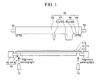
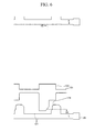
- FIG. 1 is a cross-sectional view of an exemplary embodiment of an apparatus for manufacturing a display panel according to the present invention.
- the exemplary embodiment of an apparatus for manufacturing a display panel according to the present invention includes an arriving part 40, a mold driver 50, a mold 60, and an alignment sensor 70.
- the display panel 10 which is the target of the work to be performed by the apparatus, is shown with a dotted line as it is not a part of the apparatus itself.
- the display panel 10 includes a substrate 12, a thin film 14 to be patterned, and a display panel alignment key 16.
- the work target display panel 10 is deposited on the arriving part 40 which includes a fixing chuck 42 for preventing the display panel 10 from moving during the production process and a support 46 for supporting the fixing chuck 42.
- the fixing chuck 42 includes at least one of a vacuum chuck and a static electricity chuck to hold the display panel 10 in place.
- a light transmitting part 44 is formed in the fixing chuck 42.
- the light transmitting part 44 allows an alignment sensor 70 to determine the state of alignment of the display panel 10 and the mold 60.
- the light transmitting part is formed to have a wider cross-sectional area than the cross-sectional area of the display panel alignment key 16.
- the light transmitting part 44 may be a hole penetrating the fixing chuck or a hole which is blocked by transparent glass, etc., so that light may transmit therethrough.
- the mold 60 which is driven by the mold driver 50, is arranged so that it may be brought into contact with the arriving part 40.
- the mold 60 includes a main body 62, a pattern forming part 64 which protrudes from the main body 62 toward the arriving part 40 and which has a predetermined pattern, and a mold alignment key 66.
- the pattern forming part 64 includes different shapes of protrusions 64a and 64b for forming a specific pattern when brought into contact with the display panel 10.
- the mold alignment key 66 is formed in a position of the mold 60 corresponding to the display panel alignment key 16.
- the mold alignment key 66 includes a protrusion 66a and a recess 66b which is surrounded by the protrusion 66a.
- a non-transparent film 68 is uniformly provided on the surface of the mold alignment key 66 for reflecting or absorbing an irradiated sensing light .
- the irradiated sensing light may be provided by the alignment sensor 70 or by another light source (not shown).
- the non-transparent film 68 includes at least one of a metal film, a metal oxide film, and an inorganic film.
- the protrusion 66a and the recess 66b of the mold alignment key 66 are visually identified due to the non-transparent film 68 which is formed on the protrusion 66a and the recess 66b. Therefore, an aligned state can be easily confirmed with the display panel alignment key 16 seen on the backdrop of the mold alignment key.
- the alignment sensor 70 is provided under the arriving part 40.
- the alignment sensor 70 can confirm an aligned state of the display panel alignment key 16 and the mold alignment key 66 by detecting irradiated sensing light which is returned through the light transmitting part 44.
- an ultraviolet light irradiating part for hardening an organic film may be positioned in the upper part of the mold 60.
- the alignment sensor 70 is disposed in a lower part of the arriving part 40, there is an advantage that the mold driver 50 and the ultraviolet light irradiating part (not shown), which are positioned in the mold part of the apparatus for manufacturing a display panel are easily substituted with other molds possibly having different patterning parts. Additionally, with the mold driver 50 positioned at an upper part of the display panel 10 and an ultraviolet light irradiating part (not shown) for ultraviolet hardening also positioned above the display panel 10, an imprint lithography process can be easily performed even in a narrow space, thereby improving manufacturing efficiency.
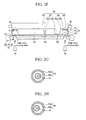
- FIGS. 2A to 2K an exemplary embodiment of a method of manufacturing a display panel according to the present invention will be described with reference to FIGS. 2A to 2K.
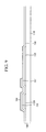
- FIG. 2A is a top plan view of a display panel in an intermediate step of an exemplary embodiment of a method of manufacturing a display panel according to the present invention
- FIG. 2B is a cross-sectional view of the display panel taken along line IIb-IIb' of FIG. 2A
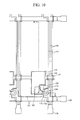
- FIGS. 2C to FIG. 2F are cross-sectional views of a display panel and an apparatus for manufacturing a display panel in intermediate steps of an exemplary embodiment of a method of manufacturing a display panel according to the present invention.
- FIGS. 2G and 2H are views illustrating the position relationship of a first alignment key and a second alignment key in ⁇ A' region of FIG. 2F as seen from an alignment sensor below an arriving part, FIGS.
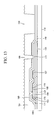
- FIG. 2I and 2J are cross-sectional views of a display panel and an apparatus for manufacturing a display panel in intermediate steps of an exemplary embodiment of a method of manufacturing a display panel according to the present invention
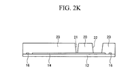
- FIG. 2K is a cross-sectional view of a display panel in an intermediate step of an exemplary embodiment of a method of manufacturing a display panel according to the present invention.
- a display panel 10 which is the target of the manufacturing process, is provided.
- the display panel 10 is used in a flat display device such as an organic light emitting diode display (“OLED”), a plasma display device (“PDP”), an electrophoresis display device (“EPD”), or other similar displays, in addition to a liquid crystal display.
- OLED organic light emitting diode display
- PDP plasma display device
- EPD electrophoresis display device
- the display panel 10 is provided with a display area and a non-display area, wherein the non-display area is formed around the display area.
- the display panel 10 includes a substrate 12 consisting of transparent glass or other materials with similar characteristics, a thin film 14, and a display panel alignment key 16, wherein the thin film 14 and the panel alignment key 16 are formed on the substrate 12.
- the thin film 14 may be a thin film in which a specific pattern is already formed or a thin film which requires formation of a specific pattern.
- the specific pattern may be a signal line for driving a display device, a recess, a protrusion, or other similar patterns.
- the thin film 14 is formed only in the display area, in alternative configurations it may also be formed in the non-display area.
- the display panel alignment keys 16 are individually formed in two opposite corners along a longitudinal side of the non-display area of the display panel 10. These display panel alignment keys 16 will be used in determining an alignment position of the display panel 10.
- the display panel alignment keys 16 are formed by patterning a thin film including at least one of a metal film, a metal oxidation film, and an inorganic film on the substrate 12.
- the display panel alignment keys 16 may be patterned by an imprint lithography process according to the present exemplary embodiment, as well as by a photolithography process.
- Alternative exemplary embodiments include configurations where the display panel alignment keys 16 may be individually formed in two opposite corners of a lateral side of a non-display area of the display panel 10, or where they may be individually formed in two corners in a diagonal direction. Additionally, the number of the display panel alignment keys 16 may be one, three, or more as needed.
- the display panel 10 is provided to and fixed in the arriving part 40.
- an organic film 17 is coated on the display panel 10.
- the organic film 17 is coated on the display panel 10 in a jell format or a liquid format having fluidity, by a spin coating method or a slit coating method.
- the organic film 17 protects the lower thin film 14, and acts as an insulating layer for insulating other films (not shown) which may be formed above or below the thin film 14.
- the organic film 17 may from a specific pattern and perform the same function as a photosensitive film in a photolithography process. When the thin film is used in such a manner the technique is called imprint lithography.
- the organic film 17 may be hardened by heat or ultraviolet rays because it includes at least one of a thermal hardener and an ultraviolet hardener.
- the organic film 17 is applied to the display panel 10 after disposing the display panel 10 in the arriving part 40, but the present invention is not limited thereto. That is, the organic film 17 may be coated on the display panel 10 before disposing the display panel 10 on the arriving part 40.
- pressure is applied to the coated organic film 17 by the mold 60.
- the pressure is applied by positioning the mold 60 on the upper part of the organic film 17 and driving the mold driver 50 so as to form a specific pattern in the organic film 17.
- the pattern forming part 64 is composed of different shapes of protrusions 64a and 64b. Accordingly, when pressure is applied, the organic film 17 becomes a compressed organic film 18 having compressed portions 18a and 18b corresponding to the respective shapes of the protrusions 64a and 64b of the mold 60.
- Each of the pattern forming parts 64a and 64b may be formed to have a different height. If the heights thereof are properly selected, an upper surface of each of the protrusions 64a and 64b may come in complete close contact with the thin film 14 when compression is performed.
- the alignment sensor 70 is positioned in the lower part of the arriving part 40 and sensing light is irradiated toward the display panel alignment key 16 and the mold alignment key 66 on the 'A' region through the light transmitting part 44.
- the alignment sensor 70 determines whether the display panel 10 and the mold 60 are aligned.
- the display panel 10 and the mold 60 can be accurately aligned by determining an alignment position and an alignment error between the display panel alignment key 16 and the mold alignment key 66 through irradiating the sensing light so as to confirm position alignment.
- FIG. 2G shows an example where the display panel alignment key 16 and the mold alignment key 66 are accurately aligned, and shows that the display panel 10 and the mold 60 are aligned in a correct position and an alignment error between them is not generated.
- FIG. 2H because the display panel alignment key 16 and the mold alignment key 66 are not positioned in an alignment position, an alignment error is generated and thus shows that the display panel 10 and the mold 60 are not aligned in an accurate position.
- a step of correcting the alignment error is performed.
- the correcting step is performed by moving at least one of the display panel 10 and the mold 60 relative to one another before hardening the compressed organic film 18. That is, the display panel 10 and the mold 60 are accurately aligned by relatively moving at least one of the arriving part 40 and the mold 60.
- the organic film 18 is hardened by irradiating ultraviolet light to the compressed organic film 18 after positioning an ultraviolet light irradiating part (not shown) at the upper part of the mold 60, as shown in FIG. 2I.
- the mold 60 may be made of polydimethylsiloxane, which is a transparent material which passes ultraviolet light.
- the organic film 18 may be hardened by thermal hardening.
- the mold 60 may be made of an opaque material.
- the non-transparent film 68 in the B part which is positioned at a lower part of the mold alignment key 66 blocks the ultraviolet light during ultraviolet hardening of the organic film 18. Therefore, hardening at that part is not performed. Accordingly, hardening is performed throughout the organic film 18 including the compressed portions 18a and 18b except in the organic film 18 corresponding to the B region located below the mold alignment key 66.
- the mold 60 When the mold 60 is removed it comes free easily because ultraviolet hardening is not performed in the B part and the part is in a liquid state or a jell state. Therefore, damage to the non-transparent film 68 can be reduced in the process of removing the mold 60. Accordingly, even when pressure is applied and the mold 60 is subsequently removed, proper performance of the non-transparent film 68 can be ensured.
- the organic film 18 is hardened by ultraviolet rays, the non-transparent film 68 allows the mold 60 to be easily separated from the organic film by preventing the lower organic film 18 from hardening. Accordingly, a replacement time of the non-transparent film 68 is further extended, thereby reducing a manufacturing cost of the display panel.
- the B part hardening is performed via a hardening process employing separate ultraviolet light or heat after the mold 60 is removed.
- the non-transparent film 68 preferably include at least one of a metal film, a metal oxide film, and a strong inorganic film; thereby damage to the non-transparent film 68 can be reduced. Accordingly, a replacement time of the non-transparent film 68 is extended, thereby reducing a manufacturing cost of the display panel
- the organic film 17 which coated the upper part of the thin film 14 corresponding to those pattern forming parts is pushed or squeezed away from the thin film 14, leaving little or no organic film 17 where the complete close contact was made. Accordingly, referring to FIG. 2K, the organic film 20 having predetermined patterns 21 and 22 are immediately formed through a hardening process. Therefore if the forming of the organic film 20 is the last step in the manufacture of a display panel, e.g., the organic film 20 is to form a passivation layer 180 or an organic insulator 187 as described below, then an etching process is not required.
- the organic film 20 may be used as a mask in a deposition process. The areas below the thin film 20 will not receive whatever material is to be deposited thereon, while the areas left exposed will receive the deposition. If the lower thin film 14 is etched by using the patterned organic film as an etching mask, the thin film 14 can be patterned by removing the areas of the thin film 14 which are not covered by the organic film 20.
- the organic film 20 may also be used as a constituent element of the display panel 10. When the residual organic film 20 is not to be used as a constituent element of the display panel 10 it may be removed by a separate etching process, thereafter the process of imprint lithography may begin again with the now etched thin film 14 or the newly deposited layer on top of the thin film 14 becoming the new thin film 14.
- the specific pattern in order to form a specific pattern in the thin film, can be easily formed through a pressing process employing the mold 60 without processes such as exposure and development which are used an existing photo lithography process.
- a pressing process employing the mold 60 without processes such as exposure and development which are used an existing photo lithography process.
- Such a process is referred to as an imprint lithography process, and manufacturing efficiency can be improved by eliminating processes such as exposure and development that require much time and cost in a photolithography process.
- a display panel is manufactured by using an imprint lithography process which uses a pressing mold 60 according to an exemplary embodiment of the present invention, a specific material can be patterned efficiently and accurately.
- the display panel according to this exemplary embodiment of the present invention is used in a transflective liquid crystal display.
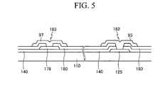
- FIG. 3 is a top plan view layout of a liquid crystal display including an exemplary embodiment of a display panel manufactured by a method of manufacturing a display panel according to the present invention
- FIGS. 4 and 5 are cross-sectional views of the liquid crystal display taken along lines IV-IV' and V-V' of FIG. 3, respectively.
- the exemplary embodiment of a liquid crystal display including a display panel manufactured according to the present invention includes a thin film transistor array panel 100, a common electrode panel 200 which is opposite thereto, and a liquid crystal layer 3 which is interposed therebetween and which includes liquid crystal molecules which are vertically or horizontally aligned with respect to the surfaces of two display panels 100 and 200.
- the liquid crystal layer 3 may be aligned by a 90° twisted nematic ("TN”) method, a vertical alignment (“VA”) method, or an electrically controlled birefringence (“ECB”) method.
- TN 90° twisted nematic
- VA vertical alignment
- EBC electrically controlled birefringence
- the insulation substrate 110 which is made of a material such as transparent glass or other similar materials.
- the insulation substrate 110 may be a separate substrate formed on top of the substrate 12.
- the insulating substrate 110 may comprise all of, or simply a part of, the substrate 12.
- the gate lines 121 mainly extend in a horizontal direction, are separated from each other, and transfer a gate signal.
- Each gate line 121 has a plurality of protrusions comprising gate electrodes 124, and an extension 125 at one end of the gate line 121 has a wide area for connecting to an external circuit (not shown).
- the storage electrode lines 131 mainly extend in a horizontal direction, and include a plurality of protrusions comprising storage electrodes 133.
- a predetermined voltage such as a common voltage which is applied to a common electrode 270 of the common electrode panel 200 is applied to the storage electrode lines 131.
- the gate lines 121 and the storage electrode lines 131 are made of aluminum metals such as aluminum (Al) or an aluminum alloy, silver metals such as silver (Ag) or a silver alloy, copper metals such as copper (Cu) or a copper alloy, molybdenum metals such as molybdenum (Mo) or a molybdenum alloy, chromium (Cr), titanium (Ti), thallium (Ta), or other substances with similar characteristics.
- aluminum metals such as aluminum (Al) or an aluminum alloy
- silver metals such as silver (Ag) or a silver alloy
- copper metals such as copper (Cu) or a copper alloy
- molybdenum metals such as molybdenum (Mo) or a molybdenum alloy
- Cr chromium
- Ti titanium
- Ta thallium
- the gate lines 121 and the storage electrode lines 131 may include two layers, e.g., a lower layer (not shown) and an upper layer (not shown) which have different physical properties.
- the upper layer may be made of metals having low resistivity, e.g., aluminum metals such as aluminum (Al) or an aluminum alloy, in order to reduce a signal delay or a voltage drop of the gate lines 121 and the storage electrode lines 131.
- the lower layer of such a configuration is made of materials such as molybdenum (Mo), a molybdenum alloy, chromium (Cr), or other similar substances, having excellent contact characteristics with other materials, specifically indium tin oxide ("ITO") and indium zinc oxide (“IZO").
- a combination of the lower layer and the upper layer may include, for example, chromium and an aluminum-neodymium (Nd) alloy.
- Alternative exemplary embodiment include configurations where the gate lines 121 and the storage electrode lines 131 may have a single layer structure or include three layers or more.
- side surfaces of the gate lines 121 and the storage electrode lines 131 are inclined relative to a surface of the substrate 110, and may have an inclination angle of about 20° to about 80°.
- a gate insulating layer 140 which is made of silicon nitride ("SiNx"), for example, is formed on the gate lines 121 and the storage electrode lines 131.
- a plurality of semiconductor stripes 151 which are made of hydrogenated amorphous silicon ("a-Si"), polycrystalline silicon, or so on are formed in an upper part of the gate insulating layer 140.
- the semiconductor stripes 151 mainly extend in a vertical direction, a plurality of protrusions 154 extend toward the gate electrodes 124 therefrom, and a plurality of extensions 157 extend therefrom. Furthermore, because the semiconductor stripes 151 have a wide width around an intersection at which they meet the gate lines 121 and the storage electrode lines 131, they essentially increase the surface area covered by the gate lines 121 and the storage electrode lines 131.
- a plurality of ohmic contact stripes and islands 161 and 165 are formed.
- the ohmic contact stripes 161 and ohmic contact islands 165 are made of a material such as n+ hydrogenated amorphous silicon in which silicide or an n-type impurity is doped with a high concentration.
- the ohmic contact stripes 161 have a plurality of protrusions 163, and the protrusions 163 and the ohmic contact islands 165 are formed in pairs and positioned on the protrusions 154 of the semiconductor stripes 151.
- Side surfaces of the semiconductor stripes 151 and the ohmic contacts 161 and 165 are also inclined to the surface of the substrate 110, and an inclination angle thereof is about 30° to about 80°.
- a plurality of data lines 171 and a plurality of drain electrodes 175, which are separated therefrom, are formed on the ohmic contacts 161 and 165 and the gate insulating layer 140.
- the data lines 171 mainly extend in a vertical direction to intersect the gate lines 121 and the storage electrode lines 131.
- the data lines 171 transfer a data voltage.
- Each data line 171 includes an extension 179 of which one end has a wide area so as to connect to other layers or an outside apparatus (not shown).
- Each drain electrode 175 includes an extension 177 which overlaps one storage electrode 133.
- the data lines 171 include a plurality of protrusions along their length, and the length portion including the protrusions constitutes a source electrode 173.
- the source electrode 173 surrounds part of one end part of a drain electrode 175.
- a gate electrode 124, a source electrode 173, a drain electrode 175 and a protrusion 154 of a semiconductor stripe 151 constitute a thin film transistor ("TFT"), and a channel of the thin film transistor is formed in the protrusion 154 between the source electrode 173 and the drain electrode 175.
- TFT thin film transistor
- the data lines 171 and the drain electrodes 175 are made of refractory metals such as tantalum, titanium, chromium and molybdenum.
- the data lines 171 and the drain electrodes 175 may have a multilayer structure consisting of a lower layer (not shown) which is made of molybdenum (Mo), a molybdenum alloy, or chromium (Cr), and an upper layer (not shown) which is made of an aluminum metal.
- the upper layer is positioned on the lower layer.
- the ohmic contact stripe 161, the protrusions on the semiconductor stripe 163 and the ohmic contact island 165 are layered between the lower semiconductors 151 and the upper data lines 171 and drain electrodes 175, and perform a function of lowering contact resistance therebetween.
- Each semiconductor stripe 151 has an exposed portion (e.g., a portion between the source electrode 173 and the drain electrode 175) which is exposed without being covered by the data line 171, the drain electrode 175, or the ohmic contacts 161, 163 and 165.
- a passivation layer 180 which is made of silicon nitride or silicon oxide, which are inorganic materials, is formed on an exposed portion of the semiconductor stripes 151, the data lines 171, and the drain electrodes 175.
- An organic insulator 187 which is made of an organic material having excellent planarization characteristics and photosensitivity, is formed above the passivation layer 180.
- a surface of the organic insulator 187 has a protrusion and depression pattern, e.g., a wavy pattern, and reflection efficiency of a reflecting electrode 194 (to be described below) to be disposed thereon is maximized thereby.
- the organic insulator 187 is removed, and only the passivation layer 180 remains.
- a contact hole 183 for exposing the extension 179 of the data line 171 and a contact hole 182 for exposing the extension 125 of the gate line 121 along with the gate insulating layer 140 is formed in the passivation layer 180. Furthermore, a contact hole 185 for exposing the extension 177 of the drain electrode 175 is formed in the passivation layer 180 and the organic insulator 187.
- the contact holes 182,183, and 185 may be formed in various shapes such as a polygonal or a circular shape, and a side wall thereof is inclined with an angle of about 30° to about 85° or may alternatively include a step shape.
- Each pixel electrode 190 includes a transparent electrode 192 and a reflecting electrode 194 which is formed on an upper part of the transparent electrode 192.
- the transparent electrode 192 is made of at least one of ITO or IZO, which are transparent conductive materials
- the reflecting electrode 194 is made of aluminum or an aluminum alloy, silver or a silver alloy, or other substances with similar characteristics, which are opaque and have reflectance.
- the pixel electrode 190 may further include a contact auxiliary layer (not shown) which is made of molybdenum or a molybdenum alloy, chromium, titanium, tantalum, or other substances with similar characteristics. The contact auxiliary layer secures contact characteristics of the transparent electrode 192 and the reflecting electrode 194, and performs a function of preventing the transparent electrode 192 from oxidizing the reflecting electrode 194.
- one pixel is largely divided into a transmitting region TA 195 and a reflecting region RA.
- the transmitting region TA 195 is a region in which the reflecting electrode 194 is removed
- the reflecting region RA is a region in which the reflecting electrode 194 is applied.
- the organic insulator 187 is removed in the transmitting region TA 195, and a cell gap, or the distance the liquid crystal layer crosses between the two substrates 100 and 200, in the transmitting region TA 195 is about two times as large as a cell gap in the reflecting region RA. Therefore, light in the reflection region RA and the transmitting region TA can be compensated for the effects of an optical path difference which is generated when light passes through the liquid crystal layer 3.
- the pixel electrodes 190 are physically and electrically connected to the extensions 177 of the drain electrodes 175 through the contact holes 185 to receive a data voltage from the drain electrodes 175.
- a pixel electrode 190 to which the data voltage is applied and the common electrode 270 generate an electric field in the liquid crystal layer 3, thereby rearranging liquid crystal molecules between them.
- each pixel electrode 190 and the common electrode 270 constitute a capacitor (hereinafter, referred to as a "liquid crystal capacitor”), they maintain an applied voltage even after the thin film transistor is turned off.
- a storage capacitor another capacitor which is connected in parallel to a liquid crystal capacitor is provided, and this capacitor is called a storage capacitor.
- the storage capacitor is formed by overlapping the extension 177 of the drain electrode 175 and the storage electrode 133.
- Alternative exemplary embodiments include the configuration where the storage capacitor may be formed by overlapping the pixel electrode 190 and the gate line 121 which is adjacent thereto.
- the storage electrode line 131 may be omitted.
- the pixel electrode 190 is overlaps the gate line 121 and the data line 171 which is adjacent thereto to increase an aperture ratio, however it does not have to overlap the gate line 121 and the data line 171.
- Alternative exemplary embodiments of the pixel electrode 190 include configurations where it comprises a transparent conductive polymer. Additionally, in the exemplary embodiment where the liquid crystal display is a reflective display the pixel electrode 190 may be made of an opaque reflective metal.
- a plurality of contact assistants 95 and 97 are formed on the passivation layer 180 at the extension of the data line 179 and the extension of the gate line 125.
- the contact assistants 95 and 97 are connected to the extensions 125 of the gate lines 121 and the extensions 179 of the data lines 171 through the contact holes 182 and 183.
- the contact assistants 95 and 97 perform a function of supplementing adhesion between, and protecting, the extensions 125 and 179 of the gate lines 121 and the data lines 171 and the outside apparatus (not shown). However, they are not essential so their application is selective. Furthermore, they may be formed at the same time as a transparent electrode 192 or a reflecting electrode 194.
- a light blocking member 220 which is referred to as a black matrix is formed on the substrate 210 which is made of an insulating material such as transparent glass and is formed in the common electrode panel 200 which is opposite to the thin film transistor array panel 100.
- the light blocking member 220 prevents light leakage between the pixel electrodes 190 of different pixels, and defines an opening region which is opposite to the pixel electrodes 190 which makes up the display region of an individual pixel.
- a plurality of color filters 230 are formed on the substrate 210 and the light blocking member 220. Each color filter 230 can display one of three primary colors such as red, green, and blue.
- the color filters 230 are disposed over the transmitting region TA 195 and the reflecting region RA.
- Each of the plurality of color filters 230 are positioned between two neighboring data lines 171, and may be arranged in a vertical direction, and connected to each other, thereby forming one stripe.
- Alternative exemplary embodiments include configurations where the color filters 230 are arranged in diagonal or triangular patterns.
- Each color filter 230 can compensate for a difference in color tone according to a difference of the number of times that light in a reflection region RA and a transmitting region TA passes the color filter 230.
- Color tone refers to the shading of a particular color.
- light may pass through the color filter 230 above a reflecting region two or more times, once on the way in from the outside and again on the way out to the outside, and yet light may pass through the color filter 230 above a transmitting region TA 195 only once.
- the thickness in the transmitting region TA is formed to be greater than a thickness in the reflection region RA.
- the difference of color tone may be compensated by equally maintaining a thickness of the color filter 230 and forming a hole in the color filter 230 of the reflection region RA.
- the common electrode 270 which is made of a transparent conductive material such as ITO or IZO, or other substance with similar characteristics, is formed on the light blocking member 220 and the color filter 230.
- a conductive layer which is made of aluminum metals such as aluminum (Al) or an aluminum alloy, silver metals such as silver (Ag) or a silver alloy, copper metals such as copper (Cu) or a copper alloy, molybdenum metals such as molybdenum (Mo) or a molybdenum alloy, chromium (Cr), titanium (Ti), thallium (Ta), or other substances with similar characteristics, is formed on the insulation substrate 110 by a method such as sputtering.
- aluminum metals such as aluminum (Al) or an aluminum alloy
- silver metals such as silver (Ag) or a silver alloy
- copper metals such as copper (Cu) or a copper alloy
- molybdenum metals such as molybdenum (Mo) or a molybdenum alloy
- Cr chromium
- Ti titanium
- Ta thallium
- an organic film for patterning is coated on the conductive layer using an imprint lithography process, which is an exemplary embodiment of a method of manufacturing a display panel according to the present invention as described above, and the organic film is patterned through a pressing process, an alignment process, a hardening process, and an etching process which uses the above-described mold.
- a plurality of storage electrode lines 131 including a plurality of storage electrodes 133 and a plurality of gate lines 121 including a plurality of gate electrodes 124 and extensions 125 are formed by etching the conductive layer using a patterned organic film as an etching mask.
- the patterned organic film which is used in the imprint lithography process performs the same function as a photosensitive film in a photolithography process, and is removed after forming the gate lines 121 and the storage electrode lines 131.
- the gate insulating layer 140 and a hydrogenated amorphous silicon film which is an amorphous silicon film that is doped with an N+ impurity, are sequentially stacked to cover the gate lines 121 and the storage electrode lines 131.
- the gate insulating layer 140 and the hydrogenated amorphous silicon film may be formed through a low temperature chemical vapor deposition ("LPCVD”) method and a plasma enhanced chemical vapor deposition (“PECVD”) method.
- LPCVD low temperature chemical vapor deposition
- PECVD plasma enhanced chemical vapor deposition
- a plurality of semiconductors 151 and a plurality of ohmic contact patterns 164 including a plurality of protrusions 154 and a plurality of extensions 157 are made of the hydrogenated amorphous silicon film using the imprint lithography process according to an exemplary embodiment of the present invention.
- the gate insulating layer 140 is made of silicon nitride, or other substances with similar characteristics.
- the patterned organic film which is used in the imprint lithography process performs the same function as a photosensitive film in a photolithography process.
- the conductive layer which is made of refractory metals such as tantalum, titanium, chromium, and molybdenum metals, is stacked by sputtering, or other suitable methods.
- a plurality of drain electrodes 175, a plurality of extensions 177, and data lines 171 including a plurality of source electrodes 173 are formed by etching the conductive layer through the imprint lithography process according to an exemplary embodiment of the present invention.
- the patterned organic film which is used in an imprint lithography process performs the same function as a photosensitive film in a photolithography process.
- the ohmic contact pattern 164 is divided into two ohmic contacts 163 and 165, and a part of the semiconductor 154 between the two is exposed by removing a part of the ohmic contact pattern 164 which is not covered by the data line 171 and the drain electrode 175. According to one exemplary embodiment, oxygen plasma is generated thereafter to stabilize a surface of the exposed semiconductor 154.
- the passivation layer 180 which is made of silicon nitride, or other substances with similar characteristics, is formed by a chemical vapor deposition ("CVD") method and is coated with an organic insulator formation material which is made of an organic material, and the organic insulator 187 is patterned through an imprint lithography process according to the an exemplary embodiment of the present invention. Since a pattern of protrusion and depression shapes may be formed in a main body of a mold (corresponding to reference numeral 60 in FIG. 2F) which is used in a pressing process, protrusion and depression shapes of the pattern are formed in the patterned organic insulator 187. The protrusion and depression shapes may be used to increase the reflection efficiency of the reflecting electrode 194 described below.
- a plurality of contact holes 185 for exposing the passivation layer 180 at an upper part of the extension 177 are formed in the organic insulator 187.
- the passivation layer 180 is exposed by removing a part of the organic insulator 187 in the transmitting region TA 195.
- the patterned organic film 20 which is used in an imprint lithography process at this step is not removed after patterning the passivation layer 180 with the organic insulator 187. This is unlike the other steps where the organic film was removed via an etching process.
- a plurality of contact holes 185 are completed by patterning the lower passivation layer 180 through an etching process using the patterned organic insulator 187.
- a plurality of transparent electrodes 192 which are connected to the drain electrode 175 through the contact hole 185 is formed through an imprint lithography process according to an exemplary embodiment of the present invention.
- the reflecting electrode 194 which is made of silver, aluminum, or other similar substances, is formed in an upper part of the transparent electrode 192 of the reflection region RA through the imprint lithography process
- the thin film transistor array panel 100 which is manufactured by an exemplary embodiment of a manufacturing method according to the present invention, which is shown in FIG. 3, is completed.
- the patterned organic film 20, which is used in an imprint lithography process for forming the transparent electrode 192 and the reflecting electrode 194, performs the same function as a photosensitive film in a photolithography process.
- a thin film itself or an etching mask pattern for etching a thin film can be easily formed without processes such as exposure and development which are included in the photolithography process.
- an alignment sensor for confirming the alignment of the display panel and the mold may be positioned in a lower part of the arriving part, a mold driver and an ultraviolet light irradiating part for ultraviolet hardening can be easily positioned above the upper part of the display panel. Therefore, an imprint lithography process can be easily performed even within a small space.
- non-transparent film in a mold alignment key is made from a metal film, a metal oxidation film, and a strong inorganic film the non-transparent film is prevented from being easily damaged when the mold is separated from the organic film.
- the non-transparent film prevents the lower organic film 18 from hardening, whereby the mold can be easily separated from the organic film. Accordingly, a replacement time of the non-transparent film 68 is further extended, thereby further reducing a manufacturing cost of the display panel.
- a predetermined thin film can be efficiently and accurately patterned according to a method of manufacturing a display panel through an imprint lithography process using an exemplary embodiment of a pressing mold of the present invention.
Landscapes
- Physics & Mathematics (AREA)
- Engineering & Computer Science (AREA)
- General Physics & Mathematics (AREA)
- Chemical & Material Sciences (AREA)
- Power Engineering (AREA)
- Crystallography & Structural Chemistry (AREA)
- Condensed Matter Physics & Semiconductors (AREA)
- Nonlinear Science (AREA)
- Nanotechnology (AREA)
- Microelectronics & Electronic Packaging (AREA)
- Computer Hardware Design (AREA)
- Mathematical Physics (AREA)
- Manufacturing & Machinery (AREA)
- Optics & Photonics (AREA)
- Life Sciences & Earth Sciences (AREA)
- Sustainable Development (AREA)
- Theoretical Computer Science (AREA)
- Mechanical Engineering (AREA)
- Multimedia (AREA)
- Devices For Indicating Variable Information By Combining Individual Elements (AREA)
- Liquid Crystal (AREA)
Applications Claiming Priority (1)
| Application Number | Priority Date | Filing Date | Title |
|---|---|---|---|
| KR1020060041435A KR101261606B1 (ko) | 2006-05-09 | 2006-05-09 | 표시판의 제조 장치 및 제조 방법 |
Publications (1)
| Publication Number | Publication Date |
|---|---|
| EP1855148A1 true EP1855148A1 (en) | 2007-11-14 |
Family
ID=38006923
Family Applications (1)
| Application Number | Title | Priority Date | Filing Date |
|---|---|---|---|
| EP07007979A Withdrawn EP1855148A1 (en) | 2006-05-09 | 2007-04-19 | Imprint / soft lithography process for flat panel displays |
Country Status (5)
| Country | Link |
|---|---|
| US (1) | US8253941B2 (ko) |
| EP (1) | EP1855148A1 (ko) |
| JP (1) | JP5253756B2 (ko) |
| KR (1) | KR101261606B1 (ko) |
| CN (1) | CN101071263B (ko) |
Cited By (1)
| Publication number | Priority date | Publication date | Assignee | Title |
|---|---|---|---|---|
| EP3410181A4 (en) * | 2016-01-27 | 2019-10-09 | Boe Technology Group Co. Ltd. | ARRAYSUBSTRAT AND DISPLAY DEVICE |
Families Citing this family (28)
| Publication number | Priority date | Publication date | Assignee | Title |
|---|---|---|---|---|
| KR101230315B1 (ko) * | 2006-02-08 | 2013-02-06 | 삼성디스플레이 주식회사 | 표시장치용 몰드와 이를 이용한 표시장치의 제조방법 |
| US7835001B2 (en) * | 2006-05-24 | 2010-11-16 | Samsung Mobile Display Co., Ltd. | Method of aligning a substrate, mask to be aligned with the same, and flat panel display apparatus using the same |
| KR101358255B1 (ko) * | 2006-06-27 | 2014-02-05 | 엘지디스플레이 주식회사 | 광경화 타입 소수성 몰드 및 그 제조방법 |
| KR100832298B1 (ko) * | 2006-06-29 | 2008-05-26 | 엘지디스플레이 주식회사 | 패턴 형성용 레지스트와 이를 이용한 소프트몰드 제조방법 |
| KR101255508B1 (ko) * | 2006-06-30 | 2013-04-16 | 엘지디스플레이 주식회사 | 플렉서블 디스플레이 및 이의 얼라인 키의 제조 방법 |
| KR101434451B1 (ko) * | 2007-03-13 | 2014-08-27 | 엘지디스플레이 주식회사 | 액정표시장치용 어레이 기판의 제조 방법 |
| KR20080088238A (ko) * | 2007-03-29 | 2008-10-02 | 삼성전자주식회사 | 패턴 형성용 몰드, 패턴 형성 장치 및 패턴 형성 방법 |
| KR101381252B1 (ko) | 2007-06-05 | 2014-04-04 | 삼성디스플레이 주식회사 | 임프린트 장치, 이의 제조 방법 및 이를 이용한 박막패터닝 방법 |
| KR101367305B1 (ko) * | 2008-02-15 | 2014-02-27 | 삼성디스플레이 주식회사 | 박막 트랜지스터 기판의 제조 방법 |
| KR101510883B1 (ko) * | 2008-06-05 | 2015-04-10 | 엘지디스플레이 주식회사 | 유기 박막트랜지스터와 그 제조방법 |
| KR101603314B1 (ko) * | 2008-09-11 | 2016-03-15 | 삼성디스플레이 주식회사 | 유기 발광 표시 장치 및 그 제조 방법 |
| NL2004932A (en) * | 2009-07-27 | 2011-01-31 | Asml Netherlands Bv | Imprint lithography template. |
| KR101105410B1 (ko) * | 2009-08-20 | 2012-01-17 | 주식회사 디엠에스 | 임프린트 장치 |
| JP5732631B2 (ja) * | 2009-09-18 | 2015-06-10 | ボンドテック株式会社 | 接合装置および接合方法 |
| KR101752020B1 (ko) | 2009-10-07 | 2017-06-28 | 데쿠세리아루즈 가부시키가이샤 | 접착 장치, 판상 접착체의 제조 방법 |
| KR101675843B1 (ko) * | 2010-05-04 | 2016-11-30 | 엘지디스플레이 주식회사 | 평판 표시 소자 및 그 제조 방법 |
| KR101726634B1 (ko) * | 2010-12-08 | 2017-04-13 | 엘지디스플레이 주식회사 | 박막 트랜지스터 기판의 제조 방법 |
| WO2013164881A1 (ja) * | 2012-05-01 | 2013-11-07 | 信越エンジニアリング株式会社 | 表示装置の製造方法及びその製造装置 |
| KR102038693B1 (ko) * | 2013-04-15 | 2019-10-31 | 삼성디스플레이 주식회사 | 유기 발광 표시 장치 |
| CN103354206B (zh) | 2013-06-27 | 2017-03-15 | 北京京东方光电科技有限公司 | 过孔制作方法、显示面板制作方法及显示面板 |
| KR102437180B1 (ko) * | 2017-12-06 | 2022-08-26 | 엘지디스플레이 주식회사 | 투명 유기발광 다이오드 표시장치 |
| TWM561222U (zh) * | 2018-01-24 | 2018-06-01 | 凌巨科技股份有限公司 | 具有共用閘極的畫素結構 |
| JP2019179716A (ja) * | 2018-03-30 | 2019-10-17 | 大日本印刷株式会社 | 有機エレクトロルミネッセンス表示装置、有機エレクトロルミネッセンス表示装置の製造方法、およびナノインプリント用モールド |
| CN109178516B (zh) * | 2018-07-25 | 2020-11-24 | 京东方科技集团股份有限公司 | 背膜去除方法及装置、显示装置 |
| CN109728054A (zh) * | 2019-01-02 | 2019-05-07 | 京东方科技集团股份有限公司 | 显示面板及其制备方法、显示装置 |
| KR20210042194A (ko) * | 2019-10-08 | 2021-04-19 | 삼성디스플레이 주식회사 | 표시 장치의 제조 방법, 및 표시 장치의 제조 장치 |
| KR102520642B1 (ko) * | 2020-12-29 | 2023-04-11 | 주식회사 기가레인 | 패턴 정렬 가능한 전사 장치 |
| KR102543024B1 (ko) * | 2021-12-31 | 2023-06-13 | (주)애니캐스팅 | 마이크로 렌즈 어레이 성형장치 |
Citations (2)
| Publication number | Priority date | Publication date | Assignee | Title |
|---|---|---|---|---|
| US20050079331A1 (en) * | 2003-09-01 | 2005-04-14 | Omron Corporation | Manufacturing method of optical device provided with resin thin film having micro-asperity pattern |
| US20050139576A1 (en) * | 2003-12-27 | 2005-06-30 | Lg.Philips Lcd Co., Ltd. | Method and apparatus for fabricating flat panel display |
Family Cites Families (34)
| Publication number | Priority date | Publication date | Assignee | Title |
|---|---|---|---|---|
| JPS61166518A (ja) * | 1985-01-18 | 1986-07-28 | Seiko Epson Corp | 液晶表示体駆動用回路基板の検査方法 |
| JPH0792696A (ja) | 1993-09-24 | 1995-04-07 | Sony Corp | 画像認識自動アライメント方法 |
| US6309580B1 (en) * | 1995-11-15 | 2001-10-30 | Regents Of The University Of Minnesota | Release surfaces, particularly for use in nanoimprint lithography |
| US5772905A (en) * | 1995-11-15 | 1998-06-30 | Regents Of The University Of Minnesota | Nanoimprint lithography |
| JP2000323461A (ja) | 1999-05-11 | 2000-11-24 | Nec Corp | 微細パターン形成装置、その製造方法、および形成方法 |
| CN100504598C (zh) | 2000-07-16 | 2009-06-24 | 得克萨斯州大学系统董事会 | 用于平版印刷工艺中的高分辨率重叠对齐方法和系统 |
| US7635262B2 (en) * | 2000-07-18 | 2009-12-22 | Princeton University | Lithographic apparatus for fluid pressure imprint lithography |
| EP2306242A3 (en) | 2000-10-12 | 2011-11-02 | Board of Regents, The University of Texas System | Method of forming a pattern on a substrate |
| US6955767B2 (en) | 2001-03-22 | 2005-10-18 | Hewlett-Packard Development Company, Lp. | Scanning probe based lithographic alignment |
| US20050064344A1 (en) * | 2003-09-18 | 2005-03-24 | University Of Texas System Board Of Regents | Imprint lithography templates having alignment marks |
| JP2003086537A (ja) | 2001-09-13 | 2003-03-20 | Tdk Corp | 構造体を用いた薄膜パターン製造方法および構造体 |
| KR100437799B1 (ko) * | 2002-04-08 | 2004-06-30 | 엘지전자 주식회사 | 디스플레이 패널 제작을 위한 잉크젯 얼라인 장치 |
| MY144124A (en) | 2002-07-11 | 2011-08-15 | Molecular Imprints Inc | Step and repeat imprint lithography systems |
| US7077992B2 (en) * | 2002-07-11 | 2006-07-18 | Molecular Imprints, Inc. | Step and repeat imprint lithography processes |
| CN100454141C (zh) | 2002-08-27 | 2009-01-21 | 奥博杜卡特股份公司 | 用于将图案转印到物体的设备 |
| AU2003266662A1 (en) | 2002-11-13 | 2004-06-03 | Sumitomo Heavy Industries, Ltd. | Aligning method and aligning device in proximity exposure |
| AU2003284410A1 (en) * | 2002-11-19 | 2004-06-15 | Ishikawa Seisakusho, Ltd. | Pixel control element selection transfer method, pixel control element mounting device used for pixel control element selection transfer method, wiring formation method after pixel control element transfer, and planar display substrate |
| JP2004259985A (ja) | 2003-02-26 | 2004-09-16 | Sony Corp | レジストパターン形成装置およびその形成方法、および、当該方法を用いた半導体装置の製造方法 |
| JP2005031662A (ja) | 2003-07-09 | 2005-02-03 | Samsung Electronics Co Ltd | アレー基板及びこれの製造方法と、これを有する液晶表示装置 |
| JP2005100584A (ja) | 2003-08-28 | 2005-04-14 | Tdk Corp | ディスク基板のインプリント方法、インプリント装置及びディスク状記録媒体の製造方法 |
| JP2005101201A (ja) | 2003-09-24 | 2005-04-14 | Canon Inc | ナノインプリント装置 |
| JP4478424B2 (ja) * | 2003-09-29 | 2010-06-09 | キヤノン株式会社 | 微細加工装置およびデバイスの製造方法 |
| JP2005116978A (ja) | 2003-10-10 | 2005-04-28 | Sumitomo Heavy Ind Ltd | ナノインプリント装置及び方法 |
| US7686606B2 (en) | 2004-01-20 | 2010-03-30 | Wd Media, Inc. | Imprint embossing alignment system |
| JP4247146B2 (ja) | 2004-03-24 | 2009-04-02 | 國煌 謝 | 電気光学素子の製造に用いられるマイクロスタンピング方法 |
| JP4954498B2 (ja) | 2004-06-01 | 2012-06-13 | 株式会社半導体エネルギー研究所 | 半導体装置の作製方法 |
| JP4574240B2 (ja) * | 2004-06-11 | 2010-11-04 | キヤノン株式会社 | 加工装置、加工方法、デバイス製造方法 |
| JP4937500B2 (ja) | 2004-06-15 | 2012-05-23 | 大日本印刷株式会社 | インプリント方法 |
| JP2006165371A (ja) * | 2004-12-09 | 2006-06-22 | Canon Inc | 転写装置およびデバイス製造方法 |
| US7363854B2 (en) * | 2004-12-16 | 2008-04-29 | Asml Holding N.V. | System and method for patterning both sides of a substrate utilizing imprint lithography |
| JP4290177B2 (ja) * | 2005-06-08 | 2009-07-01 | キヤノン株式会社 | モールド、アライメント方法、パターン形成装置、パターン転写装置、及びチップの製造方法 |
| JP4736821B2 (ja) * | 2006-01-24 | 2011-07-27 | 株式会社日立製作所 | パターン形成方法およびパターン形成装置 |
| KR20070105040A (ko) | 2006-04-25 | 2007-10-30 | 엘지.필립스 엘시디 주식회사 | 레지스트 조성물, 이를 이용한 레지스트 패턴 형성방법 및이를 이용하여 제조된 어레이 기판 |
| US7835001B2 (en) * | 2006-05-24 | 2010-11-16 | Samsung Mobile Display Co., Ltd. | Method of aligning a substrate, mask to be aligned with the same, and flat panel display apparatus using the same |
-
2006
- 2006-05-09 KR KR1020060041435A patent/KR101261606B1/ko not_active IP Right Cessation
- 2006-08-31 US US11/513,918 patent/US8253941B2/en active Active
- 2006-09-22 CN CN200610139300.3A patent/CN101071263B/zh active Active
-
2007
- 2007-04-19 EP EP07007979A patent/EP1855148A1/en not_active Withdrawn
- 2007-05-09 JP JP2007124050A patent/JP5253756B2/ja not_active Expired - Fee Related
Patent Citations (2)
| Publication number | Priority date | Publication date | Assignee | Title |
|---|---|---|---|---|
| US20050079331A1 (en) * | 2003-09-01 | 2005-04-14 | Omron Corporation | Manufacturing method of optical device provided with resin thin film having micro-asperity pattern |
| US20050139576A1 (en) * | 2003-12-27 | 2005-06-30 | Lg.Philips Lcd Co., Ltd. | Method and apparatus for fabricating flat panel display |
Non-Patent Citations (1)
| Title |
|---|
| BRITTAIN S ET AL: "SOFT LITHOGRAPHY AND MICROFABRICATION", PHYSICS WORLD, BRISTOL, GB, vol. 11, no. 5, May 1998 (1998-05-01), pages 31 - 36, XP008022000 * |
Cited By (1)
| Publication number | Priority date | Publication date | Assignee | Title |
|---|---|---|---|---|
| EP3410181A4 (en) * | 2016-01-27 | 2019-10-09 | Boe Technology Group Co. Ltd. | ARRAYSUBSTRAT AND DISPLAY DEVICE |
Also Published As
| Publication number | Publication date |
|---|---|
| US20070262936A1 (en) | 2007-11-15 |
| US8253941B2 (en) | 2012-08-28 |
| CN101071263A (zh) | 2007-11-14 |
| KR20070109014A (ko) | 2007-11-15 |
| CN101071263B (zh) | 2014-08-06 |
| KR101261606B1 (ko) | 2013-05-09 |
| JP5253756B2 (ja) | 2013-07-31 |
| JP2007304596A (ja) | 2007-11-22 |
Similar Documents
| Publication | Publication Date | Title |
|---|---|---|
| US8253941B2 (en) | Apparatus for manufacturing display panel and method for manufacturing the same | |
| US7951527B2 (en) | Method of forming an integrated optical polarization grid on an LCD substrate and liquid crystal display manufactured to include the grid | |
| US7846618B2 (en) | Multi-tone optical mask, method of manufacturing the same and method of manufacturing thin-film transistor substrate by using the same | |
| US7518696B2 (en) | Liquid crystal display panel and method of fabricating the same having particular spacers | |
| US7750987B2 (en) | Substrate for a display device, liquid crystal display device having the same and method of manufacturing the same | |
| US20140118656A1 (en) | Liquid crystal display and manufacturing method thereof | |
| US20060033869A1 (en) | Reflective and transflective liquid crystal display devices and a fabricating method thereof | |
| US20090121232A1 (en) | Array substrate, method for manufacturing the same and display panel having the same | |
| CN101952771A (zh) | 液晶显示面板 | |
| CN107045237B (zh) | 阵列基板及其制造方法 | |
| US20180143471A1 (en) | Display device and method for fabricating the same | |
| US7851835B2 (en) | Display substrate, method of manufacturing the same and display device having the same | |
| US7368753B2 (en) | Thin film transistor array substrate and fabricating method thereof | |
| US8329486B2 (en) | Thin film transistor array panel and method for manufacturing the same | |
| TW200404185A (en) | Liquid crystal display apparatus and manufacture method of same | |
| US20100020258A1 (en) | Thin film transistor substrate, method of manufacturing thereof and liquid crystal display device | |
| US7683371B2 (en) | Display panel and method for manufacturing the same | |
| US7929104B2 (en) | Liquid crystal display and method of producing same | |
| US20070052908A1 (en) | Liquid crystal display and method for manufacturing the same | |
| KR20060101616A (ko) | 잉크젯 프린팅 시스템을 이용한 색필터 표시판 및 이를포함하는 액정 표시 장치의 제조 방법 | |
| US20070097282A1 (en) | Thin film multilayer substrate, manufacturing method thereof, and liquid crystal display having thin film multilayer substrate | |
| KR101381204B1 (ko) | 액정표시장치용 어레이 기판의 제조 방법 | |
| KR101013693B1 (ko) | 액정표시소자 및 그 제조방법 | |
| KR100430117B1 (ko) | 액정 표시 장치 및 그 제조 방법 | |
| KR20110016111A (ko) | 액정 표시 패널의 제조 방법 |
Legal Events
| Date | Code | Title | Description |
|---|---|---|---|
| PUAI | Public reference made under article 153(3) epc to a published international application that has entered the european phase |
Free format text: ORIGINAL CODE: 0009012 |
|
| AK | Designated contracting states |
Kind code of ref document: A1 Designated state(s): AT BE BG CH CY CZ DE DK EE ES FI FR GB GR HU IE IS IT LI LT LU LV MC MT NL PL PT RO SE SI SK TR |
|
| AX | Request for extension of the european patent |
Extension state: AL BA HR MK YU |
|
| 17P | Request for examination filed |
Effective date: 20080331 |
|
| 17Q | First examination report despatched |
Effective date: 20080505 |
|
| AKX | Designation fees paid |
Designated state(s): DE FR GB SK |
|
| RAP1 | Party data changed (applicant data changed or rights of an application transferred) |
Owner name: SAMSUNG ELECTRONICS CO., LTD. |
|
| RAP1 | Party data changed (applicant data changed or rights of an application transferred) |
Owner name: SAMSUNG DISPLAY CO., LTD. |
|
| RAP1 | Party data changed (applicant data changed or rights of an application transferred) |
Owner name: SAMSUNG DISPLAY CO., LTD. |
|
| STAA | Information on the status of an ep patent application or granted ep patent |
Free format text: STATUS: THE APPLICATION HAS BEEN WITHDRAWN |
|
| 18W | Application withdrawn |
Effective date: 20170803 |