EP1850210B1 - Dispositif optoélectronique permettant de déterminer les mouvements relatifs ou les positions relatives de deux objets - Google Patents
Dispositif optoélectronique permettant de déterminer les mouvements relatifs ou les positions relatives de deux objets Download PDFInfo
- Publication number
- EP1850210B1 EP1850210B1 EP07007527A EP07007527A EP1850210B1 EP 1850210 B1 EP1850210 B1 EP 1850210B1 EP 07007527 A EP07007527 A EP 07007527A EP 07007527 A EP07007527 A EP 07007527A EP 1850210 B1 EP1850210 B1 EP 1850210B1
- Authority
- EP
- European Patent Office
- Prior art keywords
- light
- optoelectronic device
- board
- relative
- light shield
- Prior art date
- Legal status (The legal status is an assumption and is not a legal conclusion. Google has not performed a legal analysis and makes no representation as to the accuracy of the status listed.)
- Active
Links
- 230000005693 optoelectronics Effects 0.000 title claims description 47
- 238000006073 displacement reaction Methods 0.000 claims description 12
- 230000002093 peripheral effect Effects 0.000 description 8
- 230000007935 neutral effect Effects 0.000 description 6
- 238000013461 design Methods 0.000 description 5
- 239000000306 component Substances 0.000 description 4
- 239000006260 foam Substances 0.000 description 3
- 239000000853 adhesive Substances 0.000 description 2
- 230000001070 adhesive effect Effects 0.000 description 2
- 239000004568 cement Substances 0.000 description 2
- 230000000694 effects Effects 0.000 description 2
- 238000005476 soldering Methods 0.000 description 2
- 238000013519 translation Methods 0.000 description 2
- 230000014616 translation Effects 0.000 description 2
- 238000013459 approach Methods 0.000 description 1
- 230000004888 barrier function Effects 0.000 description 1
- 238000004891 communication Methods 0.000 description 1
- 230000000295 complement effect Effects 0.000 description 1
- 239000008358 core component Substances 0.000 description 1
- 238000001514 detection method Methods 0.000 description 1
- 238000011161 development Methods 0.000 description 1
- 238000001746 injection moulding Methods 0.000 description 1
- 239000000463 material Substances 0.000 description 1
- 238000012986 modification Methods 0.000 description 1
- 230000004048 modification Effects 0.000 description 1
- 230000003287 optical effect Effects 0.000 description 1
- 229920003023 plastic Polymers 0.000 description 1
- 239000004033 plastic Substances 0.000 description 1
- 238000012545 processing Methods 0.000 description 1
- 239000007787 solid Substances 0.000 description 1
- 239000000758 substrate Substances 0.000 description 1
Images


Classifications
-
- G—PHYSICS
- G06—COMPUTING; CALCULATING OR COUNTING
- G06F—ELECTRIC DIGITAL DATA PROCESSING
- G06F3/00—Input arrangements for transferring data to be processed into a form capable of being handled by the computer; Output arrangements for transferring data from processing unit to output unit, e.g. interface arrangements
- G06F3/01—Input arrangements or combined input and output arrangements for interaction between user and computer
- G06F3/03—Arrangements for converting the position or the displacement of a member into a coded form
- G06F3/033—Pointing devices displaced or positioned by the user, e.g. mice, trackballs, pens or joysticks; Accessories therefor
- G06F3/0354—Pointing devices displaced or positioned by the user, e.g. mice, trackballs, pens or joysticks; Accessories therefor with detection of 2D relative movements between the device, or an operating part thereof, and a plane or surface, e.g. 2D mice, trackballs, pens or pucks
-
- G—PHYSICS
- G06—COMPUTING; CALCULATING OR COUNTING
- G06F—ELECTRIC DIGITAL DATA PROCESSING
- G06F3/00—Input arrangements for transferring data to be processed into a form capable of being handled by the computer; Output arrangements for transferring data from processing unit to output unit, e.g. interface arrangements
- G06F3/01—Input arrangements or combined input and output arrangements for interaction between user and computer
- G06F3/03—Arrangements for converting the position or the displacement of a member into a coded form
- G06F3/041—Digitisers, e.g. for touch screens or touch pads, characterised by the transducing means
- G06F3/042—Digitisers, e.g. for touch screens or touch pads, characterised by the transducing means by opto-electronic means
- G06F3/0421—Digitisers, e.g. for touch screens or touch pads, characterised by the transducing means by opto-electronic means by interrupting or reflecting a light beam, e.g. optical touch-screen
-
- G—PHYSICS
- G01—MEASURING; TESTING
- G01D—MEASURING NOT SPECIALLY ADAPTED FOR A SPECIFIC VARIABLE; ARRANGEMENTS FOR MEASURING TWO OR MORE VARIABLES NOT COVERED IN A SINGLE OTHER SUBCLASS; TARIFF METERING APPARATUS; MEASURING OR TESTING NOT OTHERWISE PROVIDED FOR
- G01D5/00—Mechanical means for transferring the output of a sensing member; Means for converting the output of a sensing member to another variable where the form or nature of the sensing member does not constrain the means for converting; Transducers not specially adapted for a specific variable
- G01D5/26—Mechanical means for transferring the output of a sensing member; Means for converting the output of a sensing member to another variable where the form or nature of the sensing member does not constrain the means for converting; Transducers not specially adapted for a specific variable characterised by optical transfer means, i.e. using infrared, visible, or ultraviolet light
- G01D5/32—Mechanical means for transferring the output of a sensing member; Means for converting the output of a sensing member to another variable where the form or nature of the sensing member does not constrain the means for converting; Transducers not specially adapted for a specific variable characterised by optical transfer means, i.e. using infrared, visible, or ultraviolet light with attenuation or whole or partial obturation of beams of light
- G01D5/34—Mechanical means for transferring the output of a sensing member; Means for converting the output of a sensing member to another variable where the form or nature of the sensing member does not constrain the means for converting; Transducers not specially adapted for a specific variable characterised by optical transfer means, i.e. using infrared, visible, or ultraviolet light with attenuation or whole or partial obturation of beams of light the beams of light being detected by photocells
-
- G—PHYSICS
- G01—MEASURING; TESTING
- G01L—MEASURING FORCE, STRESS, TORQUE, WORK, MECHANICAL POWER, MECHANICAL EFFICIENCY, OR FLUID PRESSURE
- G01L5/00—Apparatus for, or methods of, measuring force, work, mechanical power, or torque, specially adapted for specific purposes
- G01L5/16—Apparatus for, or methods of, measuring force, work, mechanical power, or torque, specially adapted for specific purposes for measuring several components of force
- G01L5/166—Apparatus for, or methods of, measuring force, work, mechanical power, or torque, specially adapted for specific purposes for measuring several components of force using photoelectric means
-
- G—PHYSICS
- G06—COMPUTING; CALCULATING OR COUNTING
- G06F—ELECTRIC DIGITAL DATA PROCESSING
- G06F3/00—Input arrangements for transferring data to be processed into a form capable of being handled by the computer; Output arrangements for transferring data from processing unit to output unit, e.g. interface arrangements
- G06F3/01—Input arrangements or combined input and output arrangements for interaction between user and computer
- G06F3/03—Arrangements for converting the position or the displacement of a member into a coded form
- G06F3/033—Pointing devices displaced or positioned by the user, e.g. mice, trackballs, pens or joysticks; Accessories therefor
- G06F3/0338—Pointing devices displaced or positioned by the user, e.g. mice, trackballs, pens or joysticks; Accessories therefor with detection of limited linear or angular displacement of an operating part of the device from a neutral position, e.g. isotonic or isometric joysticks
-
- G—PHYSICS
- G06—COMPUTING; CALCULATING OR COUNTING
- G06F—ELECTRIC DIGITAL DATA PROCESSING
- G06F3/00—Input arrangements for transferring data to be processed into a form capable of being handled by the computer; Output arrangements for transferring data from processing unit to output unit, e.g. interface arrangements
- G06F3/01—Input arrangements or combined input and output arrangements for interaction between user and computer
- G06F3/03—Arrangements for converting the position or the displacement of a member into a coded form
- G06F3/041—Digitisers, e.g. for touch screens or touch pads, characterised by the transducing means
- G06F3/042—Digitisers, e.g. for touch screens or touch pads, characterised by the transducing means by opto-electronic means
-
- G—PHYSICS
- G01—MEASURING; TESTING
- G01D—MEASURING NOT SPECIALLY ADAPTED FOR A SPECIFIC VARIABLE; ARRANGEMENTS FOR MEASURING TWO OR MORE VARIABLES NOT COVERED IN A SINGLE OTHER SUBCLASS; TARIFF METERING APPARATUS; MEASURING OR TESTING NOT OTHERWISE PROVIDED FOR
- G01D2205/00—Indexing scheme relating to details of means for transferring or converting the output of a sensing member
- G01D2205/95—Three-dimensional encoders, i.e. having codes extending in three directions
Definitions
- the present invention relates to an optoelectronic device for determining relative movements or relative positions of two objects.
- the invention also relates to a force and/or moment sensor incorporating such an optoelectronic device.
- the two- or three-dimensional displacements are detected by the peripheral device and described as a translation (X, Y, Z) and/or a rotation (A, B, C) in space. Furthermore, such displacements may be used to determine a corresponding applied force and/or moment.
- the optoelectronic device will typically include one or more measuring cell comprising a position-sensitive detector illuminated by a light-emitting element, such as a light-emitting diode (LED), for measuring displacements in multiple (i.e. up to six) degrees-of-freedom.
- a light-emitting element such as a light-emitting diode (LED)
- Examples of such devices are known from United States Patent Application Publication No. 2003/102422 A1 and United States Patent Application Publication No. 2003/103217 A1 .
- the present invention is based on the object of creating a more compact, more efficient and more easily assembled design compared with known arrangements. That is, the design of the device is preferably more flexible and should require a smaller area. Also, the design of the device should be more economical to produce and should provide even more reliable operation. This design may then be implemented in the creation of an input device for use in the office or entertainment sectors or a force/moment sensor which allows uncomplicated input in up to six degrees-of-freedom.
- the invention provides an optoelectronic device as defined by claim 1. Further, the invention provides a light shield for an optoelectronic device as defined by claim 11. The invention also provides a force and/or moment sensor which incorporates an optoelectronic device as claimed. Preferably, the force sensor is used as a pan/zoom sensor for image processing and other similar office applications. The invention further provides a keyboard for a personal computer which incorporates an optoelectronic device as claimed.
- the present invention provides an optoelectronic device according to the appended claims.
- the optoelectronic device of the invention is embodied as a force/moment sensor and is designed to function as an input device to allow uncomplicated and user-friendly motion input in up to six degrees-of-freedom in a 3D computer environment.
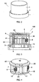
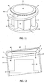
- the optoelectronic device 100 includes a frame or base 1 which typically remains stationary on a desktop or bench during use, and a knob-like cap 2 which is movably mounted on the base 1 and forms the input means with which a user may input movements to be detected and interpreted by the device 100.
- the cap 2 of the device 100 is designed to be grasped by the user and manipulated relative to the base 1 to generate the desired input.
- the lower edge of the cap is positioned in an annular recess 3 at the periphery of the base 1 with sufficient clearance to allow a degree of movement of the cap in all directions.
- the device 100 is thus designed to detect and ascertain the movements or displacements of the cap 2 relative to the base 1.
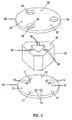
- the optoelectronic device 100 includes a first board member 10 fixed relative to the base of the device, a second circular board member 20 resiliently mounted in spaced relation to the first board member 10 and adapted for movement or displacement relative thereto, and a plurality of optoelectronic measuring cells for determining relative movements or displacements between the first and second board members.
- the first and second board members 10, 20 are substantially rigid, plate-like members which preferably comprise a printed-circuit substrate and preferably also carry at least some of the electronic components of the optoelectronic measuring cells, as is known for example from US 2003/102422 and US 2003/103217 noted earlier.
- the first and second board members 10, 20 will simply be referred to as the first board 10 and the second board 20, respectively.
- the knob-like cap 2 is rigidly fixed to the second board 20 at an outer periphery thereof. That is, the second board 20 is fixed, e.g. using cement or adhesive, in abutment with a shoulder 4 formed on an inner surface of the cap 2. Furthermore, the first board 10 is rigidly connected to the frame or base 1, typically by means of screws inserted through mounting holes 5 formed in the base and through corresponding screw-holes 11 formed in the first board 10. Thus, the movement or position of the cap 2 relative to the base frame 1 is determined by detecting and measuring relative movements and/or positions of the first board 10 and the second board 20.
- the two 'objects' for which the optoelectronic device 100 of the invention determines relative movements or positions may be understood as being the first board 10 and the second board 20. Nevertheless, the relative movements or positions of those two objects, also correspond to the relative movements or positions of the base 1 and the cap 2 to which the first board 10 and the second board 20 are respectively rigidly connected.
- the second board 20 is elastically connected to the first board 10 by three equally spaced coil spring elements 6.
- a lower end of each of the spring elements 6 is adapted to be received and fixed (preferably by soldering) within a corresponding mounting hole 12 formed in the first board 10.
- an upper end of each of the spring elements 6 is adapted to be received and fixed (again, preferably by soldering) within a corresponding mounting hole 22 formed in the second board 20.
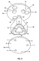
- the substantially circular second board 20 is mounted in a neutral position (shown in Fig. 4 ) spaced directly above and essentially parallel to the substantially circular first board 10, such that the second board 20 is elastically biased to the neutral position by the spring elements 6.
- the springs 6 act to return the second board 20 to the neutral position when it is moved or displaced relative to the first board 10.
- each of the measuring cells for determining the relative movements and/or positions of the first and second boards 10, 20 comprises a light emitting element in the form of an infrared light-emitting diode (ILED) 13 projecting from on an upper side the first board 10 and a position-sensitive infrared detector (PSID) 23 mounted on an underside of the second board 20, facing the first board 10.
- ILED infrared light-emitting diode
- PSID position-sensitive infrared detector
- a light shield 30 is provided between the first board 10 and the second board 20 for effectively housing the ILEDs 13 and for shielding the PSIDs 23 from any unwanted or extraneous light which might otherwise affect the accuracy of the readings the PSIDs provide.
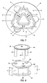
- the light shield 30 takes the form of a multi-sided (roughly triangular) prismatic housing which is designed to be mounted on the first board 10 such that it covers and encloses the ILEDs 13.
- Each PSID 23 is thereby designed to form a part of two separate measuring cells.
- the light shield housing 30 has a generally hollow structure with a number of cavities 31 that define individual light-path channels between each ILED 13 on the first board 10 and its respective PSID 23 mounted on the second board 20 above. Furthermore, as shown in Fig. 5 , the light shield housing 30 includes slit diaphragms 32 formed in a top wall 33 thereof such that each of the slit diaphragms 32 is arranged in the light-path between an ILED 13 and the respective PSID 23 that that ILED is intended to illuminate.
- each of the ILEDs 13 is arranged in a vicinity of an apex between two adjacent sides of the generally triangular housing 30 and the respective slit diaphragms 32 are centrally located along the lengths of each side at she top wall portion 33.
- the light shield housing 30 is thus configured to define a plurality of light beam paths between the ILEDs 13 on the first board 10 and the PSIDs 23 on the second board 20, such that each of the light beam paths is arranged to extend at an angle in the range of about 30° to about 60° (and preferably at about 45°) relative to the plane of the first board 10, i.e. relative to a base reference plane for the device 100. Furthermore, the light beam paths which are defined by the light-path channels 31 formed along each side of the light shield 30 thereby extend in three separate, intersecting planes corresponding to the planes of the housing sides. That is, the light beam paths of the two measuring cells having a common PSID 23 may be considered to lie within the same plane.
- the light shield housing 30 is thereby designed to form a three-dimensional array of light beam paths between the ILEDs 13 and the PSIDs 23. This, in turn, provides for a particularly compact optoelectronic device 100, while also affording great flexibility in modifications to the shape of the light shield.
- other light shield configurations including e.g. quadratic and pentagonal prisms and other multi-sided shapes, as well as curved sided shapes, are also contemplated by the present invention.
- each of the PSIDs 23 is illuminated by two separate ILEDs 13 because each of the sides of the generally three-sided light shield housing 30 is divided into two separate light-path channels 31 by a central dividing wall 34. In this way, each PSID 23 is illuminated by its two separate ILEDs 13 via two separate slit diaphragms 32.
- Each of the slits 32 provides optical communication with the associated PSID for only one of the ILEDs 13. That is, each ILED 13 is provided with its own dedicated slit diaphragm 32.
- the slit diaphragms 32 of each pair are arranged substantially parallel and extend generally perpendicular to a light-sensitive part of the associated PSID 23.
- the channels 31 on adjacent sides of the light shield housing 30 join with each other to form a V-shape recess at each of the corner regions, such that the light shield 30 comprises three V-shaped recesses separated from each other by the intermediate dividing walls 34.
- the pairs of ILEDs 13 arranged in each corner of the housing have relatively focussed light beams directed at their respective slit diaphragms 32 and PSIDs 23. Together with the design of the light shield itself, this assists in ensuring that only light from the associated ILED 13 illuminates the PSID 23.
- each pair of ILEDs 13 mounted in each corner region of the light shield 30 could be replaced by a single ILED 13 having a broader beam. In this way, each ILED 13 could then illuminate both of the light-path channels 31 extending along the adjacent sides of the housing, and thereby simultaneously illuminate two separate PSIDs 23.
- the optoelectronic device 100 further includes a stop arrangement 40 which is designed to provide a physical barrier to movement or displacement of the second board 20 relative to the first board 10 beyond a specific predetermined limit.
- the stop arrangement 40 thereby prevents any inadvertent overloading of the device 100 during use.
- the stop 40 comprises three generally elongate cylindrical stud or pin members 41 which are interconnected with one another at one end thereof via a plate-like connecting member 42.
- the three pin members 41 are equally spaced apart from one another and extend substantially parallel from one side of the plate member 42.
- the pin members 41 are adapted to be received through corresponding openings or holes 24 formed through the second board 20 and to extend towards the base 1 to be rigidly secured relative thereto.
- the pin members 41 are arranged to align with the mounting holes 5 in the base 1 used for rigidly securing the first board 10.
- the pin members 41 are preferably also secured relative to the base 1 using the same mounting holes 5.
- the pin members 41 are preferably provided with an internally threaded bore at their ends distal from the plate member 42. Alternatively, the distal ends of the pin members 41 could be secured to the first board 10 using an adhesive cement or other fastening means.
- the stop 40 has a generally robust and rigid structure for defining a solid limit to movement of the second board 20 relative to the first board 10.
- the pin members 41 and the rigid plate member 42 may be separately formed and preassembled as a sub-assembly of the optoelectronic device 100, the stop 40 is more preferably formed as a rigid unitary component, e.g. by injection molding using a relatively high-density polymer-plastics material.
- the openings or holes 24 formed through the second board 20 have a diameter substantially larger than the diameter of the pin members 41 they receive.
- each of the pin members 41 is positioned substantially centrally in its respective hole 24 through the second board.
- three elastomeric elements 7 in the form of rectangular foam blocks are disposed between the first board 10 and the second board 20.
- the elastomeric blocks 7 may be attached to an underside of the second board member 20 at positions closely adjacent to one of the pin members 41. In this way, as the second board member 20 is displaced or moved such that an edge of the hole 24 approaches a point of contact with a lateral side of the respective pin member 41, the elastomeric block 7 is adapted to come into contact with the pin 41 and thereby dampen or cushion the contact between the second board member 20 and the pin member of the stop.
- the foam blocks 7 may be mounted to extend from the second board 20 towards the first board 10, while terminating with a small gap between an end thereof and the first board. As the second board 20 is moved or displaced towards the first board member 10, the elastomeric blocks 7 initially have no effect while the displacement is within the limits of the gap. Upon further displacement of the second board 20 towards the first board 10, however, the free end of at least one of the elastomeric blocks 7 comes into contact with the first board member 10 to cushion or dampen the movement of the second board 20 before it engages the stop 40.
- the foam blocks 7 may be mounted, e.g. adhered, to outer surfaces of the light shield 30 or may be mounted on the first board 10.
- the plate member 42 connecting the upper ends of the pin members 41 of the stop 40 comprises an annular peripheral region 43 in which the surface is pitched at a specific predetermined angle relative to the neutral orientation angle of the second board 20 to thereby define a maximum angle of tilt of the second board member 20 (and the cap 2) relative to the first board member 10 (and the base frame 1) of the device.
- Such an angled annular peripheral region 43 may be provided on both an upper side and an underside of the plate member 42, as is apparent from Fig. 12 .
- a tilting (i.e. rotational) movement is applied to the second board 20 (via the cap 2) as shown, the second board 20 will deflect until, after a predetermined amount of tilting has occurred, the second board 20 engages the plate member 42 in the angled peripheral region 43.
- the contact or engagement with the angled peripheral surface region 43 of the fixed plate member 42 acts to stop further relative movement of the second board 20 in that direction.
- an upper inside surface of the cap 2 may engage a corresponding angled peripheral portion 43 of the plate member 42 as indicated in Fig. 12 .
- the first board 10, the light shield 30 and the stop 40 all remain stationary relative to the frame of the device 100, while the cap 2 and the second board 20 are moved relative thereto during operation of the device.
Claims (14)
- Dispositif optoélectronique (100) pour déterminer des mouvements relatifs ou des positions relatives de deux objets, comprenant :un premier objet (10) fixe par rapport à un châssis (1) du dispositif ;un deuxième objet (20) monté selon une relation espacée sur le premier objet (10) et adapté à un mouvement par rapport à celui-ci ;une pluralité de cellules de mesure pour déterminer un mouvement ou un déplacement du deuxième objet (20) par rapport au premier objet (10), dans lequel chaque cellule de mesure comprend un détecteur sensible à la position (23) et un élément émetteur de lumière (13) pour éclairer le détecteur sensible à la position (23) ;caractérisé parun pare-lumière (30) prévu entre le premier et le deuxième objets (10, 20) et définissant des canaux de passage de lumière (31) individuels entre l'élément émetteur de lumière (13) et le détecteur sensible à la position (23) de chaque cellule de mesure, dans lequel les canaux de passage de lumière (31) du pare-lumière (30) définissent une matrice tridimensionnelle de chemins de lumière pour les cellules de mesure entre le premier et le deuxième objets (10, 20), dans lequel le pare-lumière (30) est sous la forme d'un logement avec des cavités ou des conduites définissant les canaux de passage de lumière (31) qui dirigent la lumière dans une matrice tridimensionnelle de chemins des éléments émetteurs de lumière (13) jusqu'au détecteur sensible à la position (23) de chaque cellule de mesure entre le premier et le deuxième objets (10, 20), et dans lequel les canaux de passage de lumière (31) sont agencés dans le pare-lumière (30) de façon à définir des chemins de lumière qui sont inclinés selon un angle par rapport à un plan de référence du dispositif (100), le plan de référence correspondant préférablement à un plan du châssis (1) du dispositif (100), et/ou à un plan du premier objet (10).
- Dispositif optoélectronique (100) selon la revendication 1, dans lequel les canaux de passage de lumière (31) sont agencés dans le pare-lumière (30) de façon à ce que les chemins de lumière s'étendent dans des plans séparés entre le premier et le deuxième objets (10, 20), lesdits plans séparés se coupant préférablement les uns les autres.
- Dispositif optoélectronique (100) selon la revendication 1 ou 2, dans lequel les canaux de passage de lumière (31) du pare-lumière (30) définissent des chemins de faisceau de lumière qui sont inclinés selon un angle entre 0° et 90° par rapport au plan de référence.
- Dispositif optoélectronique (100) selon l'une quelconque des revendications 1 à 3, dans lequel chaque cellule de mesure inclut en outre un diaphragme à fente (32) agencé dans le chemin de lumière entre le détecteur sensible à la position (23) et l'élément émetteur de lumière (13), au moins un du détecteur (23), de l'élément émetteur de lumière (13) et du diaphragme à fente (32) de chaque cellule de mesure étant associé avec le premier objet (10) et étant fixe par rapport au châssis (1) du dispositif (100), et au moins un autre du détecteur (23), de l'élément émetteur de lumière (13) et du diaphragme à fente (32) de chaque cellule de mesure étant associé avec le deuxième objet (20) et étant mobile avec celui-ci.
- Dispositif optoélectronique (100) selon la revendication 4, dans lequel les canaux de passage de lumière (31) définis par le logement de pare-lumière (30) s'étendent entre chaque élément émetteur de lumière (13) et son diaphragme à fente (32) associé, le logement (30) incorporant au moins un, et préférablement chacun, des diaphragmes à fente (32) dans une partie de paroi (33) dans celui-ci.
- Dispositif optoélectronique (100) selon l'une quelconque des revendications 1 à 5, dans lequel le pare-lumière (30) comprend un logement ayant au moins trois côtés, le long de chacun desquels côtés au moins un canal de passage de lumière (31) est formé.
- Dispositif optoélectronique (100) selon la revendication 6, dans lequel deux canaux de passage de lumière (31) séparés sont formés sur chacun desdits côtés du logement de pare-lumière.
- Dispositif optoélectronique (100) selon l'une quelconque des revendications 1 à 7, dans lequel au moins un détecteur sensible à la position (23) est éclairé par deux éléments émetteurs de lumière (13) séparés pour ainsi former deux cellules de mesure avec un détecteur commun.
- Dispositif optoélectronique (100) selon la revendication 8, dans lequel chacune desdites deux cellules de mesure avec le détecteur (23) commun a un diaphragme à fente (32) séparé agencé dans le chemin de faisceau de l'élément émetteur de lumière (13) correspondant, les deux diaphragmes à fente (32) étant préférablement agencés de façon adjacente l'un à l'autre, préférablement en parallèle, dans une partie de paroi du pare-lumière (30).
- Dispositif optoélectronique (100) selon la revendication 8 ou la revendication 9, dans lequel le pare-lumière (30) définit des canaux de passage de lumière (31) séparés des éléments émetteurs de lumière (13) jusqu'au détecteur sensible à la position (23) commun.
- Dispositif optoélectronique (100) selon l'une quelconque des revendications 1 à 10, dans lequel le logement de pare-lumière a une structure unitaire.
- Dispositif optoélectronique (100) selon l'une quelconque des revendications 1 à 11, dans lequel le pare-lumière (30) inclut en outre des diaphragmes à fente (32) dans des parties de paroi (33) des canaux de passage de lumière (31).
- Capteur de force et/ou de moment incorporant un dispositif optoélectronique (100) selon l'une quelconque des revendications 1 à 12.
- Clavier pour un ordinateur personnel incorporant un dispositif optoélectronique (100) selon l'une quelconque des revendications 1 à 12.
Applications Claiming Priority (1)
| Application Number | Priority Date | Filing Date | Title |
|---|---|---|---|
| EP06007195A EP1843243B1 (fr) | 2006-04-05 | 2006-04-05 | Dispositif optoélectronique permettant de déterminer les mouvements relatifs ou les positions relatives de deux objets |
Related Parent Applications (3)
| Application Number | Title | Priority Date | Filing Date |
|---|---|---|---|
| EP06007195.8 Division | 2006-04-05 | ||
| EP06007195A Division-Into EP1843243B1 (fr) | 2006-04-05 | 2006-04-05 | Dispositif optoélectronique permettant de déterminer les mouvements relatifs ou les positions relatives de deux objets |
| EP06007195A Division EP1843243B1 (fr) | 2006-04-05 | 2006-04-05 | Dispositif optoélectronique permettant de déterminer les mouvements relatifs ou les positions relatives de deux objets |
Publications (3)
| Publication Number | Publication Date |
|---|---|
| EP1850210A2 EP1850210A2 (fr) | 2007-10-31 |
| EP1850210A3 EP1850210A3 (fr) | 2008-02-27 |
| EP1850210B1 true EP1850210B1 (fr) | 2012-02-01 |
Family
ID=36968913
Family Applications (4)
| Application Number | Title | Priority Date | Filing Date |
|---|---|---|---|
| EP07007527A Active EP1850210B1 (fr) | 2006-04-05 | 2006-04-05 | Dispositif optoélectronique permettant de déterminer les mouvements relatifs ou les positions relatives de deux objets |
| EP06007195A Active EP1843243B1 (fr) | 2006-04-05 | 2006-04-05 | Dispositif optoélectronique permettant de déterminer les mouvements relatifs ou les positions relatives de deux objets |
| EP07724090A Active EP2005278B1 (fr) | 2006-04-05 | 2007-04-05 | Dispositif optoélectronique pour déterminer des mouvements relatifs ou des positions relatives de deux objets |
| EP07724087A Withdrawn EP2005277A2 (fr) | 2006-04-05 | 2007-04-05 | Dispositif optoélectronique pour déterminer des mouvements relatifs ou des positions relatives de deux objets |
Family Applications After (3)
| Application Number | Title | Priority Date | Filing Date |
|---|---|---|---|
| EP06007195A Active EP1843243B1 (fr) | 2006-04-05 | 2006-04-05 | Dispositif optoélectronique permettant de déterminer les mouvements relatifs ou les positions relatives de deux objets |
| EP07724090A Active EP2005278B1 (fr) | 2006-04-05 | 2007-04-05 | Dispositif optoélectronique pour déterminer des mouvements relatifs ou des positions relatives de deux objets |
| EP07724087A Withdrawn EP2005277A2 (fr) | 2006-04-05 | 2007-04-05 | Dispositif optoélectronique pour déterminer des mouvements relatifs ou des positions relatives de deux objets |
Country Status (6)
| Country | Link |
|---|---|
| US (2) | US8243024B2 (fr) |
| EP (4) | EP1850210B1 (fr) |
| JP (1) | JP5155996B2 (fr) |
| KR (1) | KR20090006072A (fr) |
| CN (1) | CN101410776B (fr) |
| WO (2) | WO2007115812A2 (fr) |
Families Citing this family (47)
| Publication number | Priority date | Publication date | Assignee | Title |
|---|---|---|---|---|
| EP1998243A1 (fr) | 2007-05-25 | 2008-12-03 | 3Dconnexion Holding SA | Dispositif optoélectronique et élément souple correspondant |
| GB2462081A (en) * | 2008-07-21 | 2010-01-27 | Eigenlabs Ltd | A programmable sound creation interface |
| EP2255935B1 (fr) * | 2009-05-28 | 2012-06-20 | Max Co., Ltd. | Agrafeuse électrique |
| JP2011065409A (ja) * | 2009-09-17 | 2011-03-31 | Seiko Epson Corp | 光学式位置検出装置および位置検出機能付き表示装置 |
| JP5493674B2 (ja) * | 2009-10-13 | 2014-05-14 | セイコーエプソン株式会社 | 光検出器、光学式位置検出装置および位置検出機能付き表示装置 |
| TW201139997A (en) * | 2010-05-05 | 2011-11-16 | Edison Opto Corp | Partition type optical sensing device |
| JP2014052664A (ja) * | 2010-12-22 | 2014-03-20 | Sony Computer Entertainment Inc | 操作子及び操作装置 |
| WO2012170844A2 (fr) | 2011-06-09 | 2012-12-13 | Bloom Energy Corporation | Structures de diodes de dérivation pour piles à combustible et procédés de fixation |
| CN104995495B (zh) | 2013-03-12 | 2018-02-06 | 史赛克公司 | 用于测量力和转矩的传感器组件和方法 |
| KR102095013B1 (ko) * | 2013-04-11 | 2020-03-31 | 삼성디스플레이 주식회사 | 플렉서블 장치 |
| CN105723198B (zh) * | 2013-11-05 | 2019-11-05 | 日本精工株式会社 | 力觉传感器 |
| JP2015197357A (ja) * | 2014-04-01 | 2015-11-09 | キヤノン株式会社 | 光学式力角センサおよびこれを用いた装置 |
| DE102014216389A1 (de) * | 2014-08-19 | 2016-02-25 | BSH Hausgeräte GmbH | Bedienvorrichtung für ein Haushaltsgerät mit stabil positioniertem ringförmigen Bedienelement-Vorderteil und Haushaltsgerät mit einer derartigen Bedienvorrichtung |
| US11397108B2 (en) * | 2015-06-16 | 2022-07-26 | Marquardt Gmbh | Multi-function controller and method of using same |
| US10239213B1 (en) * | 2015-11-24 | 2019-03-26 | X Development Llc | Flexure assembly for force/torque sensing |
| US10274386B2 (en) | 2016-06-20 | 2019-04-30 | X Development Llc | Retroreflective multi-axis force torque sensor |
| US10732061B2 (en) | 2017-09-07 | 2020-08-04 | X Development Llc | Unibody flexure design for displacement-based force/torque sensing |
| US11428589B2 (en) * | 2017-10-16 | 2022-08-30 | Saf-Holland, Inc. | Displacement sensor utilizing ronchi grating interference |
| US10637470B2 (en) * | 2018-01-05 | 2020-04-28 | Darfon Electronics Corp. | Optical keyswitch |
| CN108490630B (zh) * | 2018-03-12 | 2019-10-22 | Oppo广东移动通信有限公司 | 激光投射模组、深度相机和电子装置 |
| WO2019165862A1 (fr) | 2018-02-27 | 2019-09-06 | Oppo广东移动通信有限公司 | Module de projection laser, caméra de profondeur et dispositif électronique |
| CN108490572B (zh) * | 2018-03-12 | 2021-04-23 | Oppo广东移动通信有限公司 | 激光投射模组、深度相机及电子装置 |
| CN108508687B (zh) * | 2018-03-12 | 2021-06-18 | Oppo广东移动通信有限公司 | 激光投射模组、深度相机和电子装置 |
| US20200015904A1 (en) | 2018-07-16 | 2020-01-16 | Ethicon Llc | Surgical visualization controls |
| US10732060B2 (en) * | 2018-08-15 | 2020-08-04 | X Development Llc | Force/torque sensor with hardstops to limit overloading a flexure |
| US11284957B2 (en) | 2019-03-15 | 2022-03-29 | Cilag Gmbh International | Robotic surgical controls with force feedback |
| WO2020188391A1 (fr) | 2019-03-15 | 2020-09-24 | Ethicon Llc | Commandes chirurgicales robotiques à capacités de rétroaction |
| US11666401B2 (en) | 2019-03-15 | 2023-06-06 | Cilag Gmbh International | Input controls for robotic surgery |
| US11213361B2 (en) | 2019-03-15 | 2022-01-04 | Cilag Gmbh International | Robotic surgical systems with mechanisms for scaling surgical tool motion according to tissue proximity |
| US11690690B2 (en) | 2019-03-15 | 2023-07-04 | Cilag Gmbh International | Segmented control inputs for surgical robotic systems |
| CN113795214A (zh) | 2019-03-15 | 2021-12-14 | 西拉格国际有限公司 | 用于机器人外科手术的输入控件 |
| US11583350B2 (en) | 2019-03-15 | 2023-02-21 | Cilag Gmbh International | Jaw coordination of robotic surgical controls |
| US11471229B2 (en) | 2019-03-15 | 2022-10-18 | Cilag Gmbh International | Robotic surgical systems with selectively lockable end effectors |
| US11490981B2 (en) | 2019-03-15 | 2022-11-08 | Cilag Gmbh International | Robotic surgical controls having feedback capabilities |
| US11776144B2 (en) | 2019-12-30 | 2023-10-03 | Cilag Gmbh International | System and method for determining, adjusting, and managing resection margin about a subject tissue |
| US11648060B2 (en) | 2019-12-30 | 2023-05-16 | Cilag Gmbh International | Surgical system for overlaying surgical instrument data onto a virtual three dimensional construct of an organ |
| US11219501B2 (en) | 2019-12-30 | 2022-01-11 | Cilag Gmbh International | Visualization systems using structured light |
| US11284963B2 (en) | 2019-12-30 | 2022-03-29 | Cilag Gmbh International | Method of using imaging devices in surgery |
| US11744667B2 (en) | 2019-12-30 | 2023-09-05 | Cilag Gmbh International | Adaptive visualization by a surgical system |
| US11896442B2 (en) | 2019-12-30 | 2024-02-13 | Cilag Gmbh International | Surgical systems for proposing and corroborating organ portion removals |
| US11759283B2 (en) | 2019-12-30 | 2023-09-19 | Cilag Gmbh International | Surgical systems for generating three dimensional constructs of anatomical organs and coupling identified anatomical structures thereto |
| US11832996B2 (en) | 2019-12-30 | 2023-12-05 | Cilag Gmbh International | Analyzing surgical trends by a surgical system |
| US11073920B1 (en) | 2020-10-20 | 2021-07-27 | Cirque Corporation | Multi-touch input system |
| US11813746B2 (en) | 2020-12-30 | 2023-11-14 | Cilag Gmbh International | Dual driving pinion crosscheck |
| CN113188705B (zh) * | 2021-04-30 | 2022-11-25 | 华力创科学(深圳)有限公司 | 一种基于光路阻隔法的小型力传感器及六轴力传感器 |
| CN113834527A (zh) * | 2021-09-18 | 2021-12-24 | 重庆大学 | 一种压接型功率半导体结构及其内部压力在线测量方法 |
| WO2023073664A1 (fr) | 2021-11-01 | 2023-05-04 | Cilag Gmbh International | Dispositifs, systèmes, et procédés de détection de tissu et de corps étrangers pendant une opération chirurgicale |
Family Cites Families (17)
| Publication number | Priority date | Publication date | Assignee | Title |
|---|---|---|---|---|
| JP3409359B2 (ja) * | 1993-04-16 | 2003-05-26 | ソニー株式会社 | 3次元入力装置 |
| US5940180A (en) * | 1994-10-11 | 1999-08-17 | Giddings & Lewis | Laser interferometer measurement system for use with machine tools |
| JPH0949728A (ja) * | 1995-08-04 | 1997-02-18 | Omron Corp | 距離測定装置 |
| JPH10267603A (ja) * | 1996-11-22 | 1998-10-09 | Eizou Nishimura | 位置姿勢検出装置 |
| KR100291557B1 (ko) * | 1997-08-30 | 2001-06-01 | 윤종용 | 환형차폐면을사용한cd-r및dvd호환광픽업 |
| JPH11219254A (ja) * | 1998-02-04 | 1999-08-10 | Alps Electric Co Ltd | 送受信装置 |
| DE19937307A1 (de) * | 1998-08-10 | 2000-02-17 | Deutsch Zentr Luft & Raumfahrt | Verfahren zum Auslösen von technischen Steueroperationen und/oder zum Auslösen der Ausführung von technischen Funktionen sowie Anordnung zur Durchführung des Verfahrens |
| DE10034569B4 (de) * | 2000-07-14 | 2004-02-12 | Deutsches Zentrum für Luft- und Raumfahrt e.V. | Einrichtung zum Erfassen von Relativbewegungen eines Objekts |
| DE10143489C2 (de) * | 2001-09-05 | 2003-07-17 | Deutsch Zentr Luft & Raumfahrt | Anordnung zum Erfassen von Relativbewegungen zweier Objekte |
| DE10158775B4 (de) | 2001-11-30 | 2004-05-06 | 3Dconnexion Gmbh | Anordnung zum Erfassen von Relativbewegungen oder Relativpositionen zweier Objekte |
| DE10158777B4 (de) * | 2001-11-30 | 2004-05-06 | 3Dconnexion Gmbh | Anordnung zum Erfassen von Relativbewegungen oder Relativpositionen zweier Objekte |
| DE10158776B4 (de) * | 2001-11-30 | 2004-05-13 | 3Dconnexion Gmbh | Anordnung zum Erfassen von Relativbewegungen oder Relativpositionen zweier Objekte |
| WO2003088204A1 (fr) * | 2002-04-12 | 2003-10-23 | Obermeyer Henry K | Manette a axes multiples et moyen transducteur associe |
| WO2003102495A2 (fr) * | 2002-06-04 | 2003-12-11 | Zygo Corporation | Systeme de metrologie pour deplacement 3d de precision |
| DE10225418A1 (de) * | 2002-06-07 | 2004-01-08 | 3Dconnexion Gmbh | Meßvorrichtung zum Messen von Positionen oder Bewegungen |
| DE10246031A1 (de) * | 2002-10-02 | 2004-04-15 | 3Dconnexion Gmbh | Positions- und/oder Bewegungsfühler mit Überlastungsschutz |
| JP4312192B2 (ja) * | 2005-11-02 | 2009-08-12 | ミネベア株式会社 | 光学式変位センサおよび外力検出装置 |
-
2006
- 2006-04-05 EP EP07007527A patent/EP1850210B1/fr active Active
- 2006-04-05 EP EP06007195A patent/EP1843243B1/fr active Active
-
2007
- 2007-04-05 US US12/294,816 patent/US8243024B2/en active Active
- 2007-04-05 CN CN2007800111074A patent/CN101410776B/zh active Active
- 2007-04-05 KR KR1020087022986A patent/KR20090006072A/ko not_active Application Discontinuation
- 2007-04-05 US US12/294,797 patent/US8063883B2/en not_active Expired - Fee Related
- 2007-04-05 WO PCT/EP2007/003149 patent/WO2007115812A2/fr active Application Filing
- 2007-04-05 EP EP07724090A patent/EP2005278B1/fr active Active
- 2007-04-05 EP EP07724087A patent/EP2005277A2/fr not_active Withdrawn
- 2007-04-05 JP JP2009503499A patent/JP5155996B2/ja active Active
- 2007-04-05 WO PCT/EP2007/003146 patent/WO2007115809A2/fr active Application Filing
Also Published As
| Publication number | Publication date |
|---|---|
| WO2007115809A3 (fr) | 2007-11-29 |
| CN101410776B (zh) | 2011-05-18 |
| US8063883B2 (en) | 2011-11-22 |
| US20100171704A1 (en) | 2010-07-08 |
| CN101410776A (zh) | 2009-04-15 |
| EP1843243A1 (fr) | 2007-10-10 |
| US8243024B2 (en) | 2012-08-14 |
| EP2005277A2 (fr) | 2008-12-24 |
| EP1850210A2 (fr) | 2007-10-31 |
| US20100164873A1 (en) | 2010-07-01 |
| EP1850210A3 (fr) | 2008-02-27 |
| EP2005278B1 (fr) | 2012-08-15 |
| JP5155996B2 (ja) | 2013-03-06 |
| WO2007115809A2 (fr) | 2007-10-18 |
| JP2009532688A (ja) | 2009-09-10 |
| WO2007115812A3 (fr) | 2007-11-29 |
| EP1843243B1 (fr) | 2012-02-22 |
| WO2007115812A2 (fr) | 2007-10-18 |
| EP2005278A2 (fr) | 2008-12-24 |
| KR20090006072A (ko) | 2009-01-14 |
Similar Documents
| Publication | Publication Date | Title |
|---|---|---|
| EP1850210B1 (fr) | Dispositif optoélectronique permettant de déterminer les mouvements relatifs ou les positions relatives de deux objets | |
| RU2124226C1 (ru) | Компактная конструкция "мыши" | |
| US20090088250A1 (en) | Video game device with interchangeable body, interchangeable controller, and methods of use | |
| US8462358B2 (en) | Device for detecting movement and forces | |
| US6753519B2 (en) | Arrangement for the detection of relative movements or relative positions of two objects | |
| KR101390438B1 (ko) | 스펙클 네비게이션 시스템 | |
| JP3133439U (ja) | 光学式コントロールスティック信号入力装置 | |
| JP2003166806A (ja) | 2つの物体の相対運動または相対位置を検出するための装置 | |
| EP1126354B1 (fr) | Dispositif d'entree multidirectionnel | |
| JP3408357B2 (ja) | コンピュータ等の入力装置および入力処理方法 | |
| US20060158424A1 (en) | Optical slide pad | |
| US6853366B2 (en) | Articulator and optical detection cursor positioning device | |
| US6181327B1 (en) | Computer joystick | |
| JP7077428B2 (ja) | 入力装置 | |
| CN108351666B (zh) | 操作装置 | |
| JP3408353B2 (ja) | コンピュータ等の入力装置 | |
| EP1998243A1 (fr) | Dispositif optoélectronique et élément souple correspondant | |
| US20140152625A1 (en) | Optical Touch Panel Having SMT Components As Optical Gates | |
| US8188988B2 (en) | Finger navigation device | |
| JP2017167016A (ja) | 光学スケールを有する測長器およびタッチ・プローブ | |
| JPH09128139A (ja) | コンピュータ等の入力装置 | |
| JP2018012405A (ja) | シフト装置 | |
| JP2011108207A (ja) | 操作入力装置及び操作入力検出装置 |
Legal Events
| Date | Code | Title | Description |
|---|---|---|---|
| PUAI | Public reference made under article 153(3) epc to a published international application that has entered the european phase |
Free format text: ORIGINAL CODE: 0009012 |
|
| AC | Divisional application: reference to earlier application |
Ref document number: 1843243 Country of ref document: EP Kind code of ref document: P |
|
| AK | Designated contracting states |
Kind code of ref document: A2 Designated state(s): AT BE BG CH CY CZ DE DK EE ES FI FR GB GR HU IE IS IT LI LT LU LV MC NL PL PT RO SE SI SK TR |
|
| AX | Request for extension of the european patent |
Extension state: AL BA HR MK YU |
|
| PUAL | Search report despatched |
Free format text: ORIGINAL CODE: 0009013 |
|
| AK | Designated contracting states |
Kind code of ref document: A3 Designated state(s): AT BE BG CH CY CZ DE DK EE ES FI FR GB GR HU IE IS IT LI LT LU LV MC NL PL PT RO SE SI SK TR |
|
| AX | Request for extension of the european patent |
Extension state: AL BA HR MK YU |
|
| 17P | Request for examination filed |
Effective date: 20080805 |
|
| AKX | Designation fees paid |
Designated state(s): CH DE GB LI |
|
| 17Q | First examination report despatched |
Effective date: 20090616 |
|
| RAP1 | Party data changed (applicant data changed or rights of an application transferred) |
Owner name: SOCIETE CIVILE "GALILEO 2011" |
|
| GRAP | Despatch of communication of intention to grant a patent |
Free format text: ORIGINAL CODE: EPIDOSNIGR1 |
|
| GRAS | Grant fee paid |
Free format text: ORIGINAL CODE: EPIDOSNIGR3 |
|
| GRAA | (expected) grant |
Free format text: ORIGINAL CODE: 0009210 |
|
| AC | Divisional application: reference to earlier application |
Ref document number: 1843243 Country of ref document: EP Kind code of ref document: P |
|
| AK | Designated contracting states |
Kind code of ref document: B1 Designated state(s): CH DE GB LI |
|
| REG | Reference to a national code |
Ref country code: GB Ref legal event code: FG4D |
|
| REG | Reference to a national code |
Ref country code: CH Ref legal event code: EP |
|
| REG | Reference to a national code |
Ref country code: DE Ref legal event code: R096 Ref document number: 602006027490 Country of ref document: DE Effective date: 20120329 |
|
| REG | Reference to a national code |
Ref country code: CH Ref legal event code: PL |
|
| PLBE | No opposition filed within time limit |
Free format text: ORIGINAL CODE: 0009261 |
|
| STAA | Information on the status of an ep patent application or granted ep patent |
Free format text: STATUS: NO OPPOSITION FILED WITHIN TIME LIMIT |
|
| 26N | No opposition filed |
Effective date: 20121105 |
|
| PG25 | Lapsed in a contracting state [announced via postgrant information from national office to epo] |
Ref country code: LI Free format text: LAPSE BECAUSE OF NON-PAYMENT OF DUE FEES Effective date: 20120430 Ref country code: CH Free format text: LAPSE BECAUSE OF NON-PAYMENT OF DUE FEES Effective date: 20120430 |
|
| REG | Reference to a national code |
Ref country code: DE Ref legal event code: R097 Ref document number: 602006027490 Country of ref document: DE Effective date: 20121105 |
|
| PGFP | Annual fee paid to national office [announced via postgrant information from national office to epo] |
Ref country code: GB Payment date: 20150429 Year of fee payment: 10 |
|
| GBPC | Gb: european patent ceased through non-payment of renewal fee |
Effective date: 20160405 |
|
| PG25 | Lapsed in a contracting state [announced via postgrant information from national office to epo] |
Ref country code: GB Free format text: LAPSE BECAUSE OF NON-PAYMENT OF DUE FEES Effective date: 20160405 |
|
| PGFP | Annual fee paid to national office [announced via postgrant information from national office to epo] |
Ref country code: DE Payment date: 20230427 Year of fee payment: 18 |