EP1806602A2 - Schwarzmatrix für Farbfilter und Herstellungsverfahren der Schwarzmatrix - Google Patents
Schwarzmatrix für Farbfilter und Herstellungsverfahren der Schwarzmatrix Download PDFInfo
- Publication number
- EP1806602A2 EP1806602A2 EP06122875A EP06122875A EP1806602A2 EP 1806602 A2 EP1806602 A2 EP 1806602A2 EP 06122875 A EP06122875 A EP 06122875A EP 06122875 A EP06122875 A EP 06122875A EP 1806602 A2 EP1806602 A2 EP 1806602A2
- Authority
- EP
- European Patent Office
- Prior art keywords
- black matrix
- ink
- grooves
- light shade
- shade layer
- Prior art date
- Legal status (The legal status is an assumption and is not a legal conclusion. Google has not performed a legal analysis and makes no representation as to the accuracy of the status listed.)
- Withdrawn
Links
Images


Classifications
-
- G—PHYSICS
- G02—OPTICS
- G02B—OPTICAL ELEMENTS, SYSTEMS OR APPARATUS
- G02B5/00—Optical elements other than lenses
- G02B5/003—Light absorbing elements
-
- B—PERFORMING OPERATIONS; TRANSPORTING
- B03—SEPARATION OF SOLID MATERIALS USING LIQUIDS OR USING PNEUMATIC TABLES OR JIGS; MAGNETIC OR ELECTROSTATIC SEPARATION OF SOLID MATERIALS FROM SOLID MATERIALS OR FLUIDS; SEPARATION BY HIGH-VOLTAGE ELECTRIC FIELDS
- B03B—SEPARATING SOLID MATERIALS USING LIQUIDS OR USING PNEUMATIC TABLES OR JIGS
- B03B4/00—Separating by pneumatic tables or by pneumatic jigs
- B03B4/02—Separating by pneumatic tables or by pneumatic jigs using swinging or shaking tables
-
- B—PERFORMING OPERATIONS; TRANSPORTING
- B03—SEPARATION OF SOLID MATERIALS USING LIQUIDS OR USING PNEUMATIC TABLES OR JIGS; MAGNETIC OR ELECTROSTATIC SEPARATION OF SOLID MATERIALS FROM SOLID MATERIALS OR FLUIDS; SEPARATION BY HIGH-VOLTAGE ELECTRIC FIELDS
- B03B—SEPARATING SOLID MATERIALS USING LIQUIDS OR USING PNEUMATIC TABLES OR JIGS
- B03B4/00—Separating by pneumatic tables or by pneumatic jigs
- B03B4/04—Separating by pneumatic tables or by pneumatic jigs using rotary tables or tables formed by travelling belts
-
- B—PERFORMING OPERATIONS; TRANSPORTING
- B03—SEPARATION OF SOLID MATERIALS USING LIQUIDS OR USING PNEUMATIC TABLES OR JIGS; MAGNETIC OR ELECTROSTATIC SEPARATION OF SOLID MATERIALS FROM SOLID MATERIALS OR FLUIDS; SEPARATION BY HIGH-VOLTAGE ELECTRIC FIELDS
- B03D—FLOTATION; DIFFERENTIAL SEDIMENTATION
- B03D1/00—Flotation
-
- G—PHYSICS
- G02—OPTICS
- G02B—OPTICAL ELEMENTS, SYSTEMS OR APPARATUS
- G02B5/00—Optical elements other than lenses
- G02B5/20—Filters
- G02B5/201—Filters in the form of arrays
-
- H—ELECTRICITY
- H01—ELECTRIC ELEMENTS
- H01J—ELECTRIC DISCHARGE TUBES OR DISCHARGE LAMPS
- H01J29/00—Details of cathode-ray tubes or of electron-beam tubes of the types covered by group H01J31/00
- H01J29/02—Electrodes; Screens; Mounting, supporting, spacing or insulating thereof
- H01J29/10—Screens on or from which an image or pattern is formed, picked up, converted or stored
- H01J29/18—Luminescent screens
- H01J29/30—Luminescent screens with luminescent material discontinuously arranged, e.g. in dots, in lines
- H01J29/32—Luminescent screens with luminescent material discontinuously arranged, e.g. in dots, in lines with adjacent dots or lines of different luminescent material, e.g. for colour television
- H01J29/327—Black matrix materials
-
- H—ELECTRICITY
- H01—ELECTRIC ELEMENTS
- H01J—ELECTRIC DISCHARGE TUBES OR DISCHARGE LAMPS
- H01J9/00—Apparatus or processes specially adapted for the manufacture, installation, removal, maintenance of electric discharge tubes, discharge lamps, or parts thereof; Recovery of material from discharge tubes or lamps
- H01J9/20—Manufacture of screens on or from which an image or pattern is formed, picked up, converted or stored; Applying coatings to the vessel
- H01J9/22—Applying luminescent coatings
- H01J9/227—Applying luminescent coatings with luminescent material discontinuously arranged, e.g. in dots or lines
- H01J9/2278—Application of light absorbing material, e.g. between the luminescent areas
Definitions
- the present invention relates to a black matrix of a color filter, and more particularly, a black matrix for color filters by which ink mixture between pixels of a color filter may be prevented and the color reproducibility and contrast ratio of the color filter may be improved, and a method of manufacturing the black matrix.
- CRT monitors have been usually used to display information from TVs and computers.
- flat panel displays such as, liquid crystal displays (LCDs), plasma display panels (PDPs), electro-luminescence (EL) displays, light emitting diodes (LEDs), or field emission displays (FEDs)
- LCDs among these flat panel displays are widely used as desk-top computer monitors, lap-top computer monitors, etc. because of low power consumption.
- General LCDs include a color filter that forms images of desired colors by transmitting white light modulated by a liquid crystal layer.
- a color filter To manufacture a color filter, first, a black matrix having a predetermined shape is formed on a transparent substrate, and then inks of predetermined colors, such as, red (R), green (G), and blue (B), are injected into pixel regions defined by the black matrix using an inkjet printing method, for example, to form pixels of the predetermined colors.
- predetermined colors such as, red (R), green (G), and blue (B)
- the color filter when an upper surface and a lateral surface of the black matrix are both ink-philic, ink injected into each pixel region may overflow onto the upper surface ink and thus color mixture between pixels may occur.
- the upper surface and the lateral surface of the black matrix are both ink-phobic, the ink mixture between pixels can be prevented, but ink coated within each pixel region cannot have a uniform thickness due to the lack of wetting of the lateral surface of the black matrix with ink. Hence, light leakage around the lateral surfaces of the black matrix may occur, consequently degrading the color reproducibility and the contrast ratio of the color filter.
- the present invention provides a black matrix for color filters by which ink mixture between pixels of a color filter may be prevented and the color reproducibility and contrast ratio of the color filter may be improved, and a method of manufacturing the black matrix.
- a black matrix for color filters that is formed on a substrate and defines a plurality of pixel regions, the black matrix including: an upper surface having a plurality of nano-sized grooves formed therein and being ink-phobic; and lateral surfaces being ink-philic.
- the black matrix may be formed of an ink-philic material.
- the black matrix may be formed of polymer-based organic resin.
- Each of the grooves may be 20-200nm in size and 1000-100000nm 2 in cross-sectional area.
- the grooves may occupy 20-50% of the upper surface.
- Each of the grooves may be 50-200nm in depth.
- a color filter including: a substrate; a black matrix formed on a substrate and defining a plurality of pixel regions; and ink of predetermined colors filled within the pixel regions.
- the black matrix include: an upper surface having a plurality of nano-sized grooves formed therein and being ink-phobic; and lateral surfaces being ink-philic.
- a method of manufacturing a black matrix for color filters comprising the operations of: forming a light shade layer of an ink-philic material on a substrate; patterning the light shade layer to define a plurality of pixel regions on the substrate; and forming a black matrix by forming nano-sized grooves on an upper surface of the patterned light shade layer using a nano-imprinting process.
- the operation of forming the light shade layer may include: coating the ink-philic material on the substrate; and soft baking the ink-philic material. After the patterning of the light shade layer, the operation of hard baking the patterned light shade layer may be further included. In this case, the nano-imprinting process may be executed during the hard baking of the patterned light shade layer.
- the operation of forming the grooves using the nano-imprinting process may include: installing a stamp over the patterned light shade layer, the stamp having nano-sized protrusions formed on its bottom; pressing the stamp down on the upper surface of the patterned light shade layer so as to form grooves having shapes depending on the shapes of the protrusions in the upper surface of the patterned light shade layer; and separating the stamp from the light shade layer.
- the stamp may be formed of a material selected from the group consisting of glass, quartz, silicon (Si), and poly(dimethylsiloxane) (PDMS).
- a black matrix for color filters that is formed on a substrate and defines a plurality of pixel regions on the substrate for receiving a predetermined ink, the black matrix comprising: an upper surface being formed such that it repels the predetermined ink; and lateral surfaces that are formed such that they do not repel the predetermined ink.
- FIG. 1 is a perspective view of a black matrix 120 of a color filter according to an embodiment of the present invention.
- FIG. 2 is a cross-section of the black matrix shown in FIG. 1.
- the black matrix 120 having a predetermined shape is formed on a substrate 100.
- a plurality of pixel regions 140 are defined on the substrate 100 by the black matrix 120.
- Each of the pixel regions 140 is filled with ink of a predetermined color, and thus pixels are formed. Consequently, a color filter made up of the pixels is formed.
- the substrate 100 is transparent, and a glass substrate or a plastic substrate may be used as the transparent substrate 100.
- the black matrix 120 is formed of an ink-philic material.
- the black matrix 120 may be formed of polymer-based organic resin.
- the black matrix 120 may have a height of about 1.5 ⁇ m and a width of about 30 ⁇ m.
- An upper surface 120a of the black matrix 120 may have a concavo-convex structure. More specifically, nano-sized grooves 130 are formed on the upper surface 120a of the black matrix 120. Although the grooves 130 having circular horizontal cross-sections are illustrated in FIG. 1, the cross-sections of the grooves 130 are not limited to circles but may have the other various cross-section shapes. In the present embodiment, the grooves 130 may occupy 10-60% of the upper surface 120a of the black matrix 120. Each of the grooves 130 may be about, 10-500nm, preferably about 20-200nm, in size and about 1000-100000nm 2 , preferably, about 5000-10000nm 2 , in cross-sectional area. The size of each of the grooves 130 denotes the diameter of each groove 130 or a maximum distance between inner walls of each groove 130. The depth of each of the grooves 130 may be about 20-500nm, preferably 50-200nm.
- the upper surface 120a of the black matrix 120 is rendered ink-phobic.
- the reason why the upper surface 120a of the black matrix 120 formed of an ink-philic material has an ink-phobic characteristics is due to a lotus effect. More specifically, when the nano-sized grooves 130 are formed on the upper surface 120a of the black matrix 120, the upper surface 120a is made up of a surface of the material of the black matrix 120 and the air filled within the grooves 130.
- the nano-sized grooves 130 are formed on the upper surface 120a of the black matrix 120, an area of the upper surface 120a that contacts ink is reduced compared with when the upper surface 120a of the black matrix 120 has no concave-convex structures, that is, is flat. Hence, the surface energy on the upper surface 120a in which the grooves 130 are formed is reduced, and the contact angle with respect to ink is increased. Consequently, the upper surface 120a having the grooves 130 is rendered ink-phobic.
- the contact angle of a flat plane formed of a certain material with respect to ink is approximately 10
- the contact angle of the plane having the grooves with respect to ink is increased to about 67° .
- the upper surface 120a of the black matrix 120 is processed to have a concavo-convex structure using a physical method instead of changing the component of the black matrix 120 or chemically processing the surface of the black matrix 120, so that the upper surface 120a of the black matrix 120 is rendered ink-phobic.
- Lateral surfaces 120b of the black matrix 120 formed of an ink-philic material are kept ink-philic.
- the upper surface 120a having the grooves 130 has a tendency to repel, not combine with, or not attract ink.
- lateral surfaces 120b are formed such that they have a tendency to attract, combine with, or not repel ink.
- the ink may be a water-based ink and may be suitable for being injected or inkjet printed.
- FIG. 3 is a color filter manufactured using the black matrix 120.
- the color filter includes the substrate 100, the black matrix 120 formed on the substrate 10 and defining pixel regions, and ink of predetermined colors, such as, red (R), green (G), and blue (B), filled in the regions.
- the upper surface 120a of the black matrix 120 has the nano-sized grooves 130 formed therein, the upper surface 120a is ink-phobic. Accordingly, when pixels are formed by injecting ink into the pixel regions using an inkjet printing method, for example, color mixture between pixels can be prevented.
- the lateral surfaces 120b of the black matrix 120 are ink-philic, ink can be coated within the pixel regions to have uniform thicknesses. Hence, the color reproducibility and the contrast ratio of the color filter can be improved.
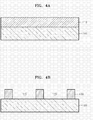
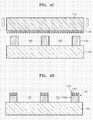
- FIGS. 4A through 4D are cross-sectional views illustrating a method of manufacturing the black matrix 120.
- a light shade layer 110 formed of an ink-philic material is formed on the substrate 100.
- the light shade layer 110 may be formed by coating the ink-philic material to a predetermined thickness on the substrate 100 and soft baking the same.
- the substrate 100 is transparent and may be a glass substrate or a plastic substrate.
- the ink-philic material may be polymer-based organic resin.
- the ink-philic material may be coated on the substrate 100 using a method, such as, spin coating, die coating, or dip coating.
- the soft baking may be executed at about 80-120 °C for about 30 seconds to 2 minutes.
- the light shade layer 110 is patterned into a patterned light shade layer 120'.
- the patterned light shade layer 120' defines a plurality of pixel regions 140 on the substrate 100.
- the patterning of the light shade layer 110 may be achieved by exposing the light shade layer 110 to light using a photomask (not shown) having a predetermined pattern.
- photoresist (not shown) is coated on the surface of the light shade layer 110 and patterned by lithography.
- the light shade layer 110 is etched using the patterned photoresist as an etch mask.
- the patterned light shade layer 120' may be about 1.5 ⁇ m in height and about 30 ⁇ m in width.
- the patterned light shade layer 120' is hard baked.
- the hard baking may be performed at about 200-230 ° C for about 20 - 40 minutes.
- the nano-sized grooves may be formed on the upper surface of the patterned light shade layer 120' using a nano-imprinting process.
- a stamp 150 is installed over the patterned light shade layer 120'.
- the stamp 150 has nano-sized protrusions 160 formed on its bottom.
- the stamp 150 may be formed of a material selected from the group consisting of glass, quartz, silicon (Si), and poly(dimethylsiloxane) (PDMS).
- PDMS poly(dimethylsiloxane)
- the grooves 130 formed on the upper surface 120a of the black matrix 120 using the nano-imprinting process may be about 20-200nm in size and about 1000-100000nm 2 , preferably, about 5000-10000nm 2 , in cross-sectional area.
- the grooves 130 may occupy 20-50% of the upper surface 120a of the black matrix 120.
- the depth of each of the grooves 130 may be about 50-200nm.
- the nano-sized grooves 130 are formed on the upper surface 120a of the black matrix 120, the upper surface 120a is rendered ink-phobic, and the lateral surfaces 120b of the black matrix 120 are rendered ink-philic.
- the upper surface of a black matrix according to the present invention may be rendered ink-phobic by making the upper surface of the black matrix have a concavo-convex structure using a physical method.
- a color filter is manufactured using the black matrix, ink mixture between pixels of the color filter can be prevented.
- the lateral surfaces of the black matrix are kept ink-philic, the color reproducibility and contrast ratio of the color filter can be improved.
Landscapes
- Physics & Mathematics (AREA)
- General Physics & Mathematics (AREA)
- Optics & Photonics (AREA)
- Engineering & Computer Science (AREA)
- Manufacturing & Machinery (AREA)
- Optical Filters (AREA)
- Liquid Crystal (AREA)
- Optical Elements Other Than Lenses (AREA)
Applications Claiming Priority (1)
| Application Number | Priority Date | Filing Date | Title |
|---|---|---|---|
| KR1020060001675A KR100790866B1 (ko) | 2006-01-06 | 2006-01-06 | 컬러 필터용 블랙 매트릭스 및 그 제조방법 |
Publications (2)
| Publication Number | Publication Date |
|---|---|
| EP1806602A2 true EP1806602A2 (de) | 2007-07-11 |
| EP1806602A3 EP1806602A3 (de) | 2007-11-07 |
Family
ID=38001962
Family Applications (1)
| Application Number | Title | Priority Date | Filing Date |
|---|---|---|---|
| EP06122875A Withdrawn EP1806602A3 (de) | 2006-01-06 | 2006-10-24 | Schwarzmatrix für Farbfilter und Herstellungsverfahren der Schwarzmatrix |
Country Status (4)
| Country | Link |
|---|---|
| US (1) | US20070157839A1 (de) |
| EP (1) | EP1806602A3 (de) |
| JP (1) | JP2007183587A (de) |
| KR (1) | KR100790866B1 (de) |
Cited By (2)
| Publication number | Priority date | Publication date | Assignee | Title |
|---|---|---|---|---|
| EP2186118A4 (de) * | 2007-08-28 | 2013-10-23 | Agency Science Tech & Res | Verfahren zur herstellung eines organischen elektronischen oder optoelektronischen bauelements |
| WO2015189735A1 (en) * | 2014-06-13 | 2015-12-17 | Semiconductor Energy Laboratory Co., Ltd. | Display device |
Families Citing this family (19)
| Publication number | Priority date | Publication date | Assignee | Title |
|---|---|---|---|---|
| KR100785031B1 (ko) * | 2006-11-22 | 2007-12-12 | 삼성전자주식회사 | 컬러 필터용 블랙 매트릭스 및 그 제조방법 |
| WO2009113615A1 (ja) * | 2008-03-13 | 2009-09-17 | 富士フイルム株式会社 | 感光性樹脂組成物、感光性樹脂硬化膜および遮光性画像形成方法 |
| KR20100123973A (ko) * | 2009-05-18 | 2010-11-26 | 삼성전자주식회사 | 컬러 필터, 그 제조 장치 및 그 제조 방법 |
| JP2010286615A (ja) * | 2009-06-10 | 2010-12-24 | Sony Corp | 光学部品の製造方法、光学部品、表示装置の製造方法および表示装置 |
| KR101591922B1 (ko) | 2009-10-20 | 2016-02-05 | 삼성디스플레이 주식회사 | 표시판 |
| KR20140119266A (ko) * | 2013-03-28 | 2014-10-10 | 삼성디스플레이 주식회사 | 유기발광 표시장치 및 그 제조방법 |
| WO2015072316A1 (ja) * | 2013-11-14 | 2015-05-21 | 堺ディスプレイプロダクト株式会社 | カラーフィルタ基板、表示装置、及びカラーフィルタ基板の製造方法 |
| CN104882468B (zh) * | 2015-06-09 | 2017-12-15 | 京东方科技集团股份有限公司 | 有机电致发光显示基板及其制作方法、显示装置 |
| US11207478B2 (en) | 2016-03-25 | 2021-12-28 | Rai Strategic Holdings, Inc. | Aerosol production assembly including surface with micro-pattern |
| US9955584B2 (en) * | 2016-04-25 | 2018-04-24 | Winbond Electronics Corp. | Stamp for printed circuit process and method of fabricating the same and printed circuit process |
| US11297876B2 (en) * | 2017-05-17 | 2022-04-12 | Rai Strategic Holdings, Inc. | Aerosol delivery device |
| KR102179729B1 (ko) | 2018-03-27 | 2020-11-17 | 주식회사 엘지화학 | 블랙 격벽 패턴 필름 및 이의 제조방법 |
| CN110534548A (zh) * | 2019-08-06 | 2019-12-03 | 武汉华星光电半导体显示技术有限公司 | Oled显示面板 |
| CN110993646B (zh) * | 2019-11-08 | 2022-07-12 | 深圳市华星光电半导体显示技术有限公司 | Oled背板的制备方法及oled背板 |
| KR102934063B1 (ko) | 2020-06-05 | 2026-03-04 | 삼성디스플레이 주식회사 | 표시 장치 |
| KR102892879B1 (ko) | 2020-06-22 | 2025-11-28 | 삼성디스플레이 주식회사 | 디스플레이 장치 |
| CN111769143B (zh) * | 2020-06-23 | 2022-09-09 | 武汉华星光电半导体显示技术有限公司 | 显示面板及其制造方法 |
| KR20220110409A (ko) | 2021-01-29 | 2022-08-08 | 삼성디스플레이 주식회사 | 표시 장치 |
| CN113013211B (zh) | 2021-02-24 | 2022-10-25 | 京东方科技集团股份有限公司 | 显示基板及其制备方法、显示装置 |
Family Cites Families (24)
| Publication number | Priority date | Publication date | Assignee | Title |
|---|---|---|---|---|
| JPS5975205A (ja) * | 1982-10-25 | 1984-04-27 | Seiko Epson Corp | カラ−フイルタの製造方法 |
| JPH07104117A (ja) * | 1993-09-30 | 1995-04-21 | Sekisui Chem Co Ltd | ディスプレー用カラーフィルタ |
| JP2872594B2 (ja) * | 1993-11-24 | 1999-03-17 | キヤノン株式会社 | カラーフィルターの製造方法及び液晶パネルの製造方法 |
| JP2000162425A (ja) * | 1998-11-30 | 2000-06-16 | Canon Inc | カラーフィルタとその製造方法、液晶素子 |
| GB9929752D0 (en) * | 1999-12-17 | 2000-02-09 | Secr Defence | Textured surface |
| JP2001183516A (ja) * | 1999-12-27 | 2001-07-06 | Canon Inc | カラーフィルタとその製造方法、該カラーフィルタを用いた液晶素子 |
| JP2002006129A (ja) * | 2000-06-19 | 2002-01-09 | Canon Inc | 光学素子とその製造方法、液晶素子 |
| KR100835912B1 (ko) | 2001-10-19 | 2008-06-09 | 엘지디스플레이 주식회사 | 액정표시장치의 컬러필터기판 제조방법 |
| KR100469390B1 (ko) | 2001-12-27 | 2005-02-02 | 엘지전자 주식회사 | 액정 표시장치의 컬러필터 제조방법 |
| EP1474835A1 (de) * | 2002-02-01 | 2004-11-10 | Koninklijke Philips Electronics N.V. | Strukturiertes polmersubstrat für ink-jet druck einer oled-matrix |
| JP2004111166A (ja) * | 2002-09-18 | 2004-04-08 | Hitachi Ltd | 有機el素子用バンク付き基板 |
| GB0302485D0 (en) * | 2003-02-04 | 2003-03-05 | Plastic Logic Ltd | Pixel capacitors |
| JP2005063785A (ja) * | 2003-08-11 | 2005-03-10 | Ran Technical Service Kk | 隔壁パターン及びその形成方法 |
| US7156032B2 (en) * | 2003-08-22 | 2007-01-02 | Lucent Technologies Inc. | Method and apparatus for controlling friction between a fluid and a body |
| JP4317113B2 (ja) * | 2003-10-30 | 2009-08-19 | 三星モバイルディスプレイ株式會社 | 平板表示装置の製造方法 |
| JP2005173107A (ja) * | 2003-12-10 | 2005-06-30 | Dainippon Printing Co Ltd | 遮光層付き光学シート及びカラーフィルタ |
| JP5005164B2 (ja) * | 2004-03-03 | 2012-08-22 | 株式会社ジャパンディスプレイイースト | 発光素子,発光型表示装置及び照明装置 |
| US20050211505A1 (en) * | 2004-03-26 | 2005-09-29 | Kroupenkine Timofei N | Nanostructured liquid bearing |
| US7172842B2 (en) * | 2004-05-12 | 2007-02-06 | Chunghwa Picture Tubes, Ltd. | Color filter array plate and method of fabricating the same |
| JP2006072176A (ja) * | 2004-09-06 | 2006-03-16 | Seiko Epson Corp | バンク、カラーフィルタ、表示装置及び電子機器 |
| KR20060024949A (ko) | 2004-09-15 | 2006-03-20 | 삼성전자주식회사 | 컬러필터기판 및 그의 제조 방법 |
| DE202004018784U1 (de) * | 2004-12-03 | 2005-03-17 | Koob Ron | Rückfahrkamera mit Lotus-Effekt |
| KR20060080760A (ko) | 2005-01-06 | 2006-07-11 | 삼성전자주식회사 | 컬러 필터 기판 및 그의 제조 방법 |
| JP4327108B2 (ja) * | 2005-02-03 | 2009-09-09 | 株式会社リコー | 光情報記録媒体の製造方法及び金型の製造方法 |
-
2006
- 2006-01-06 KR KR1020060001675A patent/KR100790866B1/ko not_active Expired - Lifetime
- 2006-10-20 US US11/583,831 patent/US20070157839A1/en not_active Abandoned
- 2006-10-24 EP EP06122875A patent/EP1806602A3/de not_active Withdrawn
- 2006-12-01 JP JP2006326097A patent/JP2007183587A/ja active Pending
Cited By (4)
| Publication number | Priority date | Publication date | Assignee | Title |
|---|---|---|---|---|
| EP2186118A4 (de) * | 2007-08-28 | 2013-10-23 | Agency Science Tech & Res | Verfahren zur herstellung eines organischen elektronischen oder optoelektronischen bauelements |
| WO2015189735A1 (en) * | 2014-06-13 | 2015-12-17 | Semiconductor Energy Laboratory Co., Ltd. | Display device |
| US20150362776A1 (en) | 2014-06-13 | 2015-12-17 | Semiconductor Energy Laboratory Co., Ltd. | Display Device |
| US10342124B2 (en) | 2014-06-13 | 2019-07-02 | Semiconductor Energy Laboratory Co., Ltd. | Display device |
Also Published As
| Publication number | Publication date |
|---|---|
| KR20070074051A (ko) | 2007-07-12 |
| EP1806602A3 (de) | 2007-11-07 |
| JP2007183587A (ja) | 2007-07-19 |
| US20070157839A1 (en) | 2007-07-12 |
| KR100790866B1 (ko) | 2008-01-03 |
Similar Documents
| Publication | Publication Date | Title |
|---|---|---|
| US20070157839A1 (en) | Black matrix of color filter and method of manufacturing the black matrix | |
| CN107393939B (zh) | 像素界定层及制造方法、显示面板及制造方法、显示装置 | |
| CN108538886B (zh) | 像素界定层及制造方法、显示基板、显示装置 | |
| CN107248523B (zh) | 像素界定层及其制造方法 | |
| WO2016086728A1 (zh) | 像素界定层及其制作方法、显示面板和显示装置 | |
| CN104979484A (zh) | 有机发光二极管显示器件及其制造方法 | |
| CN108630734B (zh) | 像素界定结构及其制备方法以及显示面板和显示装置 | |
| CN107623022A (zh) | 像素界定层及其制备方法、显示基板及其制备方法、显示装置 | |
| EP4170721A1 (de) | Anzeigetafel und herstellungsverfahren dafür | |
| JP5037145B2 (ja) | カラーフィルタ製造方法 | |
| US7816010B2 (en) | Black matrix for color filter and its method of manufacture | |
| CN101013220B (zh) | 滤色片黑矩阵的制造方法 | |
| US20070184363A1 (en) | Method of manufacturing a black matrix of color filter | |
| US20080124634A1 (en) | Method of manufacturing liquid crystal display | |
| CN102183806A (zh) | 彩色滤光数组及其制造方法 | |
| CN101013219B (zh) | 制备滤色器的黑矩阵的方法 | |
| US20080166641A1 (en) | Method of manufacturing color filter | |
| CN210428036U (zh) | 一种彩色电子墨水显示屏结构 | |
| US20090017388A1 (en) | Substrate structure for color filter and color filter having the same | |
| EP1818695A1 (de) | Vorrichtung zur Herstellung von Farbfiltern | |
| CN112271200A (zh) | 显示面板及其制备方法、显示装置 | |
| EP1607996A2 (de) | Verfahren zur Herstellung einer Phosphorschicht-Struktur | |
| US20090011344A1 (en) | Method of manufacturing color filter |
Legal Events
| Date | Code | Title | Description |
|---|---|---|---|
| PUAI | Public reference made under article 153(3) epc to a published international application that has entered the european phase |
Free format text: ORIGINAL CODE: 0009012 |
|
| AK | Designated contracting states |
Kind code of ref document: A2 Designated state(s): AT BE BG CH CY CZ DE DK EE ES FI FR GB GR HU IE IS IT LI LT LU LV MC NL PL PT RO SE SI SK TR |
|
| AX | Request for extension of the european patent |
Extension state: AL BA HR MK YU |
|
| PUAL | Search report despatched |
Free format text: ORIGINAL CODE: 0009013 |
|
| AK | Designated contracting states |
Kind code of ref document: A3 Designated state(s): AT BE BG CH CY CZ DE DK EE ES FI FR GB GR HU IE IS IT LI LT LU LV MC NL PL PT RO SE SI SK TR |
|
| AX | Request for extension of the european patent |
Extension state: AL BA HR MK YU |
|
| 17P | Request for examination filed |
Effective date: 20080206 |
|
| 17Q | First examination report despatched |
Effective date: 20080305 |
|
| AKX | Designation fees paid |
Designated state(s): DE FR GB |
|
| GRAP | Despatch of communication of intention to grant a patent |
Free format text: ORIGINAL CODE: EPIDOSNIGR1 |
|
| STAA | Information on the status of an ep patent application or granted ep patent |
Free format text: STATUS: THE APPLICATION IS DEEMED TO BE WITHDRAWN |
|
| 18D | Application deemed to be withdrawn |
Effective date: 20111006 |