EP1801774B1 - Datentreiber, organische lichtemittierende Anzeige und Verfahren zu ihrer Ansteuerung - Google Patents
Datentreiber, organische lichtemittierende Anzeige und Verfahren zu ihrer Ansteuerung Download PDFInfo
- Publication number
- EP1801774B1 EP1801774B1 EP06256515A EP06256515A EP1801774B1 EP 1801774 B1 EP1801774 B1 EP 1801774B1 EP 06256515 A EP06256515 A EP 06256515A EP 06256515 A EP06256515 A EP 06256515A EP 1801774 B1 EP1801774 B1 EP 1801774B1
- Authority
- EP
- European Patent Office
- Prior art keywords
- group
- line
- voltage
- voltage dividing
- dividing resistors
- Prior art date
- Legal status (The legal status is an assumption and is not a legal conclusion. Google has not performed a legal analysis and makes no representation as to the accuracy of the status listed.)
- Not-in-force
Links
Images



Classifications
-
- G—PHYSICS
- G09—EDUCATION; CRYPTOGRAPHY; DISPLAY; ADVERTISING; SEALS
- G09G—ARRANGEMENTS OR CIRCUITS FOR CONTROL OF INDICATING DEVICES USING STATIC MEANS TO PRESENT VARIABLE INFORMATION
- G09G3/00—Control arrangements or circuits, of interest only in connection with visual indicators other than cathode-ray tubes
- G09G3/20—Control arrangements or circuits, of interest only in connection with visual indicators other than cathode-ray tubes for presentation of an assembly of a number of characters, e.g. a page, by composing the assembly by combination of individual elements arranged in a matrix no fixed position being assigned to or needed to be assigned to the individual characters or partial characters
- G09G3/22—Control arrangements or circuits, of interest only in connection with visual indicators other than cathode-ray tubes for presentation of an assembly of a number of characters, e.g. a page, by composing the assembly by combination of individual elements arranged in a matrix no fixed position being assigned to or needed to be assigned to the individual characters or partial characters using controlled light sources
- G09G3/30—Control arrangements or circuits, of interest only in connection with visual indicators other than cathode-ray tubes for presentation of an assembly of a number of characters, e.g. a page, by composing the assembly by combination of individual elements arranged in a matrix no fixed position being assigned to or needed to be assigned to the individual characters or partial characters using controlled light sources using electroluminescent panels
-
- G—PHYSICS
- G09—EDUCATION; CRYPTOGRAPHY; DISPLAY; ADVERTISING; SEALS
- G09G—ARRANGEMENTS OR CIRCUITS FOR CONTROL OF INDICATING DEVICES USING STATIC MEANS TO PRESENT VARIABLE INFORMATION
- G09G3/00—Control arrangements or circuits, of interest only in connection with visual indicators other than cathode-ray tubes
- G09G3/20—Control arrangements or circuits, of interest only in connection with visual indicators other than cathode-ray tubes for presentation of an assembly of a number of characters, e.g. a page, by composing the assembly by combination of individual elements arranged in a matrix no fixed position being assigned to or needed to be assigned to the individual characters or partial characters
- G09G3/2007—Display of intermediate tones
- G09G3/2011—Display of intermediate tones by amplitude modulation
-
- G—PHYSICS
- G09—EDUCATION; CRYPTOGRAPHY; DISPLAY; ADVERTISING; SEALS
- G09G—ARRANGEMENTS OR CIRCUITS FOR CONTROL OF INDICATING DEVICES USING STATIC MEANS TO PRESENT VARIABLE INFORMATION
- G09G3/00—Control arrangements or circuits, of interest only in connection with visual indicators other than cathode-ray tubes
- G09G3/20—Control arrangements or circuits, of interest only in connection with visual indicators other than cathode-ray tubes for presentation of an assembly of a number of characters, e.g. a page, by composing the assembly by combination of individual elements arranged in a matrix no fixed position being assigned to or needed to be assigned to the individual characters or partial characters
-
- H—ELECTRICITY
- H03—ELECTRONIC CIRCUITRY
- H03M—CODING; DECODING; CODE CONVERSION IN GENERAL
- H03M1/00—Analogue/digital conversion; Digital/analogue conversion
- H03M1/66—Digital/analogue converters
- H03M1/68—Digital/analogue converters with conversions of different sensitivity, i.e. one conversion relating to the more significant digital bits and another conversion to the less significant bits
-
- G—PHYSICS
- G09—EDUCATION; CRYPTOGRAPHY; DISPLAY; ADVERTISING; SEALS
- G09G—ARRANGEMENTS OR CIRCUITS FOR CONTROL OF INDICATING DEVICES USING STATIC MEANS TO PRESENT VARIABLE INFORMATION
- G09G2310/00—Command of the display device
- G09G2310/02—Addressing, scanning or driving the display screen or processing steps related thereto
- G09G2310/0264—Details of driving circuits
- G09G2310/027—Details of drivers for data electrodes, the drivers handling digital grey scale data, e.g. use of D/A converters
-
- G—PHYSICS
- G09—EDUCATION; CRYPTOGRAPHY; DISPLAY; ADVERTISING; SEALS
- G09G—ARRANGEMENTS OR CIRCUITS FOR CONTROL OF INDICATING DEVICES USING STATIC MEANS TO PRESENT VARIABLE INFORMATION
- G09G2320/00—Control of display operating conditions
- G09G2320/02—Improving the quality of display appearance
- G09G2320/0223—Compensation for problems related to R-C delay and attenuation in electrodes of matrix panels, e.g. in gate electrodes or on-substrate video signal electrodes
-
- G—PHYSICS
- G09—EDUCATION; CRYPTOGRAPHY; DISPLAY; ADVERTISING; SEALS
- G09G—ARRANGEMENTS OR CIRCUITS FOR CONTROL OF INDICATING DEVICES USING STATIC MEANS TO PRESENT VARIABLE INFORMATION
- G09G2320/00—Control of display operating conditions
- G09G2320/02—Improving the quality of display appearance
- G09G2320/0252—Improving the response speed
-
- G—PHYSICS
- G09—EDUCATION; CRYPTOGRAPHY; DISPLAY; ADVERTISING; SEALS
- G09G—ARRANGEMENTS OR CIRCUITS FOR CONTROL OF INDICATING DEVICES USING STATIC MEANS TO PRESENT VARIABLE INFORMATION
- G09G2330/00—Aspects of power supply; Aspects of display protection and defect management
- G09G2330/02—Details of power systems and of start or stop of display operation
- G09G2330/021—Power management, e.g. power saving
-
- G—PHYSICS
- G09—EDUCATION; CRYPTOGRAPHY; DISPLAY; ADVERTISING; SEALS
- G09G—ARRANGEMENTS OR CIRCUITS FOR CONTROL OF INDICATING DEVICES USING STATIC MEANS TO PRESENT VARIABLE INFORMATION
- G09G3/00—Control arrangements or circuits, of interest only in connection with visual indicators other than cathode-ray tubes
- G09G3/20—Control arrangements or circuits, of interest only in connection with visual indicators other than cathode-ray tubes for presentation of an assembly of a number of characters, e.g. a page, by composing the assembly by combination of individual elements arranged in a matrix no fixed position being assigned to or needed to be assigned to the individual characters or partial characters
- G09G3/22—Control arrangements or circuits, of interest only in connection with visual indicators other than cathode-ray tubes for presentation of an assembly of a number of characters, e.g. a page, by composing the assembly by combination of individual elements arranged in a matrix no fixed position being assigned to or needed to be assigned to the individual characters or partial characters using controlled light sources
- G09G3/30—Control arrangements or circuits, of interest only in connection with visual indicators other than cathode-ray tubes for presentation of an assembly of a number of characters, e.g. a page, by composing the assembly by combination of individual elements arranged in a matrix no fixed position being assigned to or needed to be assigned to the individual characters or partial characters using controlled light sources using electroluminescent panels
- G09G3/32—Control arrangements or circuits, of interest only in connection with visual indicators other than cathode-ray tubes for presentation of an assembly of a number of characters, e.g. a page, by composing the assembly by combination of individual elements arranged in a matrix no fixed position being assigned to or needed to be assigned to the individual characters or partial characters using controlled light sources using electroluminescent panels semiconductive, e.g. using light-emitting diodes [LED]
- G09G3/3208—Control arrangements or circuits, of interest only in connection with visual indicators other than cathode-ray tubes for presentation of an assembly of a number of characters, e.g. a page, by composing the assembly by combination of individual elements arranged in a matrix no fixed position being assigned to or needed to be assigned to the individual characters or partial characters using controlled light sources using electroluminescent panels semiconductive, e.g. using light-emitting diodes [LED] organic, e.g. using organic light-emitting diodes [OLED]
-
- H—ELECTRICITY
- H03—ELECTRONIC CIRCUITRY
- H03M—CODING; DECODING; CODE CONVERSION IN GENERAL
- H03M1/00—Analogue/digital conversion; Digital/analogue conversion
- H03M1/66—Digital/analogue converters
- H03M1/74—Simultaneous conversion
- H03M1/76—Simultaneous conversion using switching tree
- H03M1/765—Simultaneous conversion using switching tree using a single level of switches which are controlled by unary decoded digital signals
Definitions
- the present invention relates to a data driver, an organic light emitting display, and a method of driving the same. More particularly, the present invention relates to a data driver for enhancing image quality, an organic light emitting display, and a method of driving the same.
- flat panel display devices having reduced weight and volume compared to comparable cathode ray tubes (CRTs) have been developed.
- These flat panel display devices include for example, a liquid crystal display, a field emission display, a plasma display panel, an organic light emitting display, etc.
- These exemplary displays may operate differently to display an image.
- an organic light emitting display displays an image by using an organic light emitting diode that generates light by recombining electrons and holes.
- an organic light emitting display supplies a current corresponding to a data signal to organic light emitting diodes by employing driving, thin film transistors formed at each pixel so light may be emitted from the organic light emitting diodes.
- Such an organic light emitting display may offer certain advantages, since it may be operated with low power consumption and may provide a rapid response speed.
- An organic light emitting display may generate data signals by using data supplied from an external source.
- the organic light emitting display supplies the generated data signals to pixels and display an image of desired brightness.
- a data driver for converting the data supplied from the external source into the data signals has been considered.
- Such a data driver may include a data signal generator for converting the external data into the data signals.
- the data signal generator may include a digital-to-analog converter (hereinafter, referred to as "DAC").
- the DAC is positioned in each channel and converts the data into the data signals.
- the data signal generator may include first DACs for generating voltages depending on the values of the upper bits of the data and second DACs for generating voltages depending on the values of the lower bits of the data.
- FIG. 1 illustrates a circuit diagram of a second DAC.
- the second DAC 2 receives a first reference voltage (ref1) and a second reference voltage (ref2) from a first DAC (not illustrated).
- the first DAC receives a plurality of reference voltages from an external source.
- the first DAC selects the first reference voltage (ref1) and the second reference voltage (ref2) among the plurality of reference voltages received depending on a value of the upper bits of the data.
- the first DAC supplies the selected first and second reference voltages (ref1) and (ref2) to the second DAC 2 via a tenth switch SW 10 and an eleventh switch SW11, as illustrated in FIG. 1 .
- the tenth switch SW10 or the eleventh switch SW11 included in the first DAC may be turned on depending on the value of the upper bits of the data.
- the present invention will be described assuming that the first reference voltage (ref1) is lower than the second reference voltage (ref2).
- the second DAC 2 includes a plurality of voltage dividing resistors R1 to R7 for dividing the voltage values of the first reference voltage (ref1) and the second reference voltage (ref2).
- the second DAC2 also includes a plurality of switches SW1 to SW8 for supplying voltages divided from the voltage dividing resistors R1 to R7 to an output terminal (out).
- a tenth resistor R10 is arranged between the eleventh switch SW11 and the seventh resistor R7.
- the tenth resistor R10 compensates for the switch resistances of the tenth switch SW 10 and the eleventh switch SW11 so that the second DAC may evenly divide the reference voltages via the voltage dividing resistors R1 to R7.
- the voltage dividing resistors R1 to R7 are arranged in series.
- the voltage dividing resistors R1 to R7 evenly divide the first reference voltage (ref1) and the second reference voltage (ref2).
- the resistance value of each of the voltage dividing resistors R1 to R7 may be identical.
- the switches SW1 to SW8 are arranged to supply the voltages divided by the voltage dividing resistors R1 to R7 to the output terminal (out).
- the first switch SW 1 is arranged between a first node N1 and the output terminal (out) to supply the second reference voltage (ref2) to the output terminal (out).
- the second switch SW2 is arranged between a second node N2 and the output terminal (out) to supply the voltage value of the second node N2 to the output terminal (out).
- the third switch SW3 is arranged between a third node N3 and the output terminal (out) to supply the voltage value of the third node N3 to the output terminal (out).
- the fourth switch SW4 is arranged between a fourth node N4 and the output terminal (out) to supply the voltage value of the fourth node N4 to the output terminal (out).
- the fifth switch SW5 is arranged between a fifth node N5 and the output terminal (out) to supply the voltage value of the fifth node N5 to the output terminal (out).
- the sixth switch SW6 is arranged between a sixth node N6 and the output terminal (out) to supply the voltage value of the sixth node N6 to the output terminal (out).
- the seventh switch SW7 is arranged between a seventh node N7 and the output terminal (out) to supply the voltage value of the seventh node N7 to the output terminal (out).
- the eighth switch SW8 is arranged between an eighth node N8 and the output terminal (out) to supply the first reference voltage (ref1) to the output terminal (out).
- one of the switches SW1 to SW8 may be turned on depending on the value of the lower bits of the data, and a predetermined voltage is supplied to the output terminal (out).
- the predetermined voltage value supplied to the output terminal (out) is supplied to pixels as a data signal.
- the conventional second DAC 2 may exhibit a deterioration of its driving ability when supplying a gray scale voltage, such as an intermediate gray scale voltage (e.g., voltages of node N4 or node N5) as a data signal.
- a gray scale voltage such as an intermediate gray scale voltage (e.g., voltages of node N4 or node N5)
- an intermediate gray scale voltage e.g., voltages of node N4 or node N5
- a period of time is required before intermediate gray scale voltages corresponding to the data signals may be supplied to the pixels.
- some intermediate gray scale voltages e.g., voltages of node N1, node N2, node N6 and node N7 adjacent to the first reference voltage (ref1) and the second reference voltage (ref2) may be supplied and charged in the pixels within a shorter period of time than other intermediate gray scale voltages (e.g., voltages of node N4 or node N5).
- the voltage values of the intermediate gray scale voltages adjacent to the first reference voltage (ref1) and the second reference voltage (ref2) may be altered, as illustrated in FIG. 2 .
- the predetermined voltage may not be supplied and charged in the pixels.
- the voltage values of the intermediate gray scale voltages more centered between the first reference voltage (ref1) and the second reference voltage (ref2) may maintain approximately similar values, regardless of the voltage drop.
- a conventional organic light emitting display may operate with certain deficiencies. That is, if the resistance values of the voltage dividing resistors R1 to R7 between the first reference voltage (ref1) and the second reference voltage (ref2) are large, the driving ability of the intermediate gray scale may be deteriorated, and if the resistance values of the voltage dividing resistors R1 to R7 are small, the gray scale voltage values adjacent to the first reference voltage (ref1) and the second reference voltage (ref2) may be altered.
- US5,389,872 discloses a system for minimizing switching errors in voltages delivered to a resistive load. The system relies on varying the resistance in switches to compensate for output voltage errors.
- US2003/0090402 discloses a DAC that comprises two sets of n resistors, two power-supply voltage lines maintained at different potentials and two sets of n switches.
- OBORN K ET AL "A new digital to analog converter resistor string architecture" ASIC Conference and exhibit, 1997. Proceedings., Tenth Annual IEEE International Portland, OR, USA 7-10 Sept. 1997, New York, NY, USA, IEEE, US, 7 September 1997 (1997-09-07), pages 304-307, XP010243411 ISBN:0-7803-4283-6 discloses a resistor string architecture for implementing a DAC on a CMOS circuit process.
- the DAC uses virtual resistance coding.
- US6,037,889 discloses an apparatus which aims to improve both the matching of the integral non-linearity of multiple resistor-string based DACs connected in parallel between two different reference voltages and the charge/discharge time of the parasitic capacitances associated with middle nodes of the AC resistor strings.
- the present invention is therefore directed to a data driver, an organic light emitting display, and a method of driving the same that sets out to overcome one or more of the problems due to the limitations and disadvantages of the related art.
- an organic light emitting display as set out in claim 12.
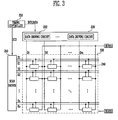
- FIG. 3 illustrates a block circuit diagram of an organic light emitting display according to an embodiment of the present invention.
- the organic light emitting display includes a pixel unit 230 including pixels 240 formed on a region where scan lines S 1 to Sn are intersected with data lines D1 to Dm, a scan driver 210 for driving scan lines S1 to Sn, a data driver 220 for driving data lines D1 to Dm, and a timing controller 250 for controlling the scan driver 210 and the data driver 220.
- the data driver 220 includes at least one data driving circuit 222.
- the scan driver 210 generates scan signals in response to scan driving control signals SCS from the timing controller 250.
- the scan driver 210 may supply the generated scan signals to the scan lines S 1 to Sn in sequence.
- the scan driver 210 generates light emitting control signals in response to the scan driving control signals SCS.
- the scan driver may supply the generated light emitting control signals to light emitting control lines E1 to En in sequence.
- the data driver 220 generates data signals in response to data driving control signals DCS from the timing controller 250.
- the data driver 220 may supply the generated data signals to the data lines D1 to Dm in sequence.
- the data driving circuit 222 converts data supplied from an external source into data signals and supplies the data signals to the data lines D 1 to Dm. The data driving circuit 222 will be described in more detail below.
- the timing controller 250 generates a data driving control signal DCS and a scan driving control signal SCS depending on synchronization signals supplied from an external source.
- the data driving control signal DCS and the scan driving control signal SCS generated from the timing controller 250 are supplied to the data driver 220 and to the scan driver 210, respectively.
- the timing controller 250 rearranges the data supplied from the external source and supplies the rearranged data DATA to the data driver 220.
- the pixel unit 230 receives a first power source ELVDD and a second power source ELVSS from an external source.
- the first power source ELVDD and the second power source ELVSS are supplied to the pixel unit 230, and aree respectively supplied to the pixels 240.
- the pixels 240 receiving the first power source ELVDD and the second power source ELVSS displays images corresponding to data signals supplied from the data driving circuit 222.
- FIG. 4A illustrates a block circuit diagram of an embodiment of the data driving circuit illustrated in FIG. 3 .
- FIG. 4A will be described assuming that the data diving circuit 222 includes "i" channels.
- the data driving circuit 222 includes the following:
- the shift register unit 223 receives a source shift clock SSC and a source start pulse SSP from the timing controller 250.
- the shift register unit 223 receiving the source shift clock SSC and the source start pulse SSP may generate "i" sampling signals in sequence, while allowing the source start pulse SSP to be shifted depending on the source shift clock SSC.
- the shift register unit 223 includes "i" shift registers 2231 to 223i.
- the sampling latch unit 224 stores data in sequence depending on the sampling signals supplied in sequence from the shift register unit 223.
- the sampling latch unit 224 includes "i" sampling latches 2241 to 224i for storing "i" data.
- Each size of the sampling latches 2241 to 224i may be set to store k bit data. For the sake of discussion, this exemplary sampling latch unit 224 will be described assuming that k bit is 6 bits.
- the holding latch unit 225 receives and stores the data from the sampling latch unit 224 in response to a source output enable SOE signal.
- the holding latch unit 225 supplies the stored data to a level shifter 226.
- the holding latch unit 225 includes "i" holding latches 2251 to 225i. Each of the holding latches 2251 to 225i may be configured to store k bit data.
- the level shifter 226 raises a voltage level of the data supplied from the holding latch unit 225 and supplies the data with a raised voltage level to the data signal generator 227.
- the data driver 220 receives data having a low voltage level and raises the voltage level of the data to a high voltage level by employing the level shifter 226.
- the data driver 220 may not include the level shifter 226.
- circuit components necessary to raise the voltage level of the data from a low voltage level to a high voltage level may be arranged external to the data driver 220. Accordingly, the holding latch unit 225 may be directly connected to the data signal generator 227. In such an arrangement, however, manufacturing costs may be increased.
- the data signal generator 227 generates data signals corresponding to bit values (or gray scale values) of the data and supplies the generated data signals to the data lines D1 to Di.
- the data signal generator 227 receives a plurality of reference voltages (refs) from a gamma voltage unit 229 and generates data signals by using the received reference voltages (refs).
- the data signal generator 227 will be described in more detail below.
- the gamma voltage unit 229 supplies the plurality of reference voltages (refs) to the data signal generator 227.
- the gamma voltage unit 229 may be arranged inside or outside of the data driving circuit 222.
- a buffer unit 228 is connected between the data signal generator 227 and the data lines D1 to Di.
- the buffer unit 228 supplies the data signals supplied from the data signal generator 227 to the data lines D1 to Di.
- FIG. 5 illustrates a block circuit diagram of an exemplary data signal generator as illustrated in FIGS. 4A and 4B .
- the data signal generator 227 includes, for each channel, a first DAC 300, a second DAC 302 and a decoder unit 304.
- the first DAC 300 receives the plurality of reference voltages (ref) from a gamma unit 229.
- the first DAC 300 selects a first reference voltage (ref1) and a second reference voltage (ref2) from the plurality of reference voltages (refs) depending on, e.g., a value of upper bits of the data.
- the first DAC 300 receives the data from the level shifter 226, or directly from the holding latch unit 225, depending on the implementation.
- the first DAC 300 supplies the first reference voltage (ref1) and the second reference voltage (ref2) to the second DAC 302 via a first line L1 and a second line L2, respectively. That is, the first DAC 300 may extract two reference voltages from the plurality of reference voltages (refs) depending on the value of the upper bits. The first DAC 300 supplies the extracted two reference voltages to the second DAC 302 as the first reference voltage (ref1) and the second reference voltage (ref2). For the sake of discussion, it will be assumed that the first reference voltage (ref1) is set to be lower than the second reference voltage (ref2).
- the second DAC 302 divides the first reference voltage (ref1) and the second reference voltage (ref2) into a plurality of voltages.
- the second DAC 302 may supply any one of the first reference voltage (ref1), the second reference voltage (ref2) and the divided voltages to the output terminal (out) as a data signal, depending on a value of the lower bits of the data.
- the decoder unit 304 controls the turning on and the turning off of switches included in the second DAC 302 depending on the value of the lower bits of the data. That is, the decoder unit 304 may control the turning on and the turning off of the switches so that a resistance value between the first line L1 and the second line L2 can be variably controlled depending on the value of the lower bits of the data.
- FIG. 6 illustrates a circuit diagram of a second DAC according to a first embodiment of the present invention.
- the second DAC 302 includes a first group of voltage dividing resistors R11 to R18, a second group of voltage dividing resistors R21 to R28, a third group of voltage dividing resistors R31 to R38, a fourth group of voltage dividing resistors R41 to R48, and a fifth group of voltage dividing resistors R51 to R58, which are arranged between the first line L 1 and the second line L2.
- the second DAC 302 also includes an arrangement of switches. The switches will be described in more detail below.
- the first group of voltage dividing resistors R11 to R18 are arranged between the first line L 1 and the second line L2 in series.
- the first group of voltage dividing resistors R11 to R18 divide the voltages of the first reference voltage (ref1) and the second reference voltage (ref2).
- the resistance values of the first group of voltage dividing resistors R11 to R18 may be identical so that the first reference voltage (ref1) and the second reference voltage (ref2) may be evenly divided.
- a first switch SW1 is arranged between the first group of voltage dividing resistors R11 to R18 and the first line L1.
- the first switch SW1 allows the first group of voltage dividing resistors R11 to R18 to be electrically connected to the first line L1 and may remain in a turned on state.
- the first switch SW 1 is arranged in order to compensate for the turn on resistances of a second switch SW2, a third switch SW3, a fourth switch SW4, and a fifth switch SW5, which will be described below.
- the second group of voltage dividing resistors R21 to R28 is arranged in parallel with the first group of voltage dividing resistors R11 to R18, and is between the first line L1 and the second line L2.
- the number of resistors in the second group of voltage dividing resistors R21 to R28 may be identical to the number of resistors in the first group of voltage dividing resistors R11 to R18.
- the second switch SW2 is arranged between the second group of voltage dividing resistors R21 to R28 and the first line L1.
- a first control signal CS1 is supplied from the decoder unit 304, and the second switch SW2 may be turned on.
- the second switch SW2 When the second switch SW2 is turned on, the second group of voltage dividing resistors R21 to R28 may be electrically connected to the first line L1. If the second group of voltage dividing resistors R21 to R28 is connected to the first line L1, the resistance value between the first line L 1 and the second line L2 may become lower than the case when only the first group of voltage dividing resistors R11 to R18 is electrically connected to first line L1 and the second line L2.
- the third group of voltage dividing resistors R31 to R38 is arranged in parallel with the second group of voltage dividing resistors R21 to R28, between the first line L1 and the second line L2.
- the number of resistors in the third group of voltage dividing resistors R31 to R38 may be identical to the number of resistors in the first group of voltage dividing resistors R11 to R18.
- the third switch SW3 is arranged between the third group of voltage dividing resistors R31 to R38 and the first line L1.
- a second control signal CS2 is supplied from the decoder unit 304, and the third switch SW3 may be turned on.
- the third switch SW3 When the third switch SW3 is turned on, the third group of voltage dividing resistors R31 to R38 may be electrically connected to the first line L1. If the third group of voltage dividing resistors R31 to R38 is connected to the first line L1, the resistance value between the first line L1 and the second line L2 may become even lower than the case when the first group of voltage dividing resistors R11 to R18 and the second group of voltage dividing resistors R21 to R28 are electrically connected to the first line L1.
- the fourth group of voltage dividing resistors R41 to R48 is arranged in parallel with the third group of voltage dividing resistors R31 to R38, between the first line L1 and the second line L2.
- the number of resistors in the fourth group of voltage dividing resistors R41 to R48 may be identical to the number of resistors in the first group of voltage dividing resistors R11 to R18.
- the fourth switch SW4 is arranged between the fourth group of voltage dividing resistors R41 to R48 and the first line L1.
- a third control signal CS3 is supplied from the decoder unit 304, and the fourth switch SW4 is turned on.
- the fourth switch SW4 is turned on, the fourth group of voltage dividing resistors R41 to R48 may be electrically connected to the first line L1. If the fourth group of voltage dividing resistors R41 to R48 is connected to the first line L1, the resistance value between the first line L1 and the second line L2 may become even lower than the case when the first voltage group of dividing resistors R11 to R18, the second group of voltage dividing resistors R21 to R28, and the third group of voltage dividing resistors R31 to R38 are electrically connected to the first line L1.
- the fifth group of voltage dividing resistors R51 to R58 is arranged in parallel with the fourth group of voltage dividing resistors R41 to R48, and is between the first line L1 and the second line L2.
- the number of resistors in the fifth group of voltage dividing resistors R51 to R58 may be identical to the number of resistors in the first group of voltage dividing resistors R11 to R18.
- the fifth switch SW5 is arranged between the fifth group of voltage dividing resistors R51 to R58 and the first line L1.
- a fourth control signal CS4 is supplied from the decoder unit 304, and the fifth switch SW5 may be turned on.
- the fifth switch SW5 When the fifth switch SW5 is turned on, the fifth group of voltage dividing resistors R51 to R58 may be electrically connected to the first line L1.
- the resistance value between the first line L1 and the second line L2 may become even lower than the case when the first group of voltage dividing resistors R11 to R18, the second group of voltage dividing resistors R21 to R28, the third group of voltage dividing resistors R31 to R38 and the fourth group of voltage dividing resistors R41 to R48 are electrically connected to the first line L1.
- FIG. 6 illustrates four voltage dividing resistor columns R21 to R28, R31 to R38, R41 to R48, and R51 to R58 that are arranged in parallel to the first group of voltage dividing resistors R11 to R18; however the present invention is not limited thereto.
- One or more voltage dividing resistor columns is in parallel with the first group of voltage dividing resistors R11 to R18.
- the second DAC 302 includes a first group of switches SW11 to SW18, a second group of switches SW21 to SW27, a third group of switches SW30 to SW37, a fourth group of switches SW41 to SW47, and a fifth group of switches SW51 to SW57.
- the first group of switches SW11 to SW18 is arranged at each node of the first group of voltage dividing resistors R11 to R18.
- the first group of switches SW11 to SW18 supplies the voltage divided in the first group of voltage dividing resistors R11 to R18 to the output terminal (out).
- an eleventh switch SW11 is arranged between a first node N1 and an output terminal (out) and supplies the second reference voltage (ref2) to the output terminal (out).
- a twelfth switch SW12 arranged between a second node N2 and the output terminal (out) supplies the voltage of the second node N2 to the output terminal (out).
- a thirteenth switch SW13 arranged between a third node N3 and the output terminal (out) supplies the voltage of the third node N3 to the output terminal (out).
- a fourteenth switch SW14 arranged between a fourth node N4 and the output terminal (out) supplies the voltage of the fourth node N4 to the output terminal (out).
- a fifteenth switch SW 15 arranged between a fifth node N5 and the output terminal (out) supplies the voltage of the fifth node N5 to the output terminal (out).
- a sixteenth switch SW16 arranged between a sixth node N6 and the output terminal (out) supplies the voltage of the sixth node N6 to the output terminal (out).
- a seventeenth switch SW17 arranged between a seventh node N7 and the output terminal (out) supplies a voltage of the seventh node N7 to the output terminal (out).
- An eighteenth switch SW18 arranged between an eighth node N8 and the output terminal (out) supplies the first reference voltage (ref1) to the output terminal (out).
- the decoder unit 304 controls the turning on and the turning off of the first group of switches SW11 to SW 18 depending on the lower bits of the data.
- the decoder unit 304 allows any one of the first group of switches SW11 to SW 18 to be turned on depending on the lower bits of the data, and the turned on switch may supply a predetermined voltage value to the output terminal (out).
- the voltage value supplied to the output terminal (out) is supplied to pixels 240 as a data signal.
- the data signal may be supplied to the pixels 240 via the buffer unit 228.
- the second group of switches SW21 to SW27 is arranged between nodes of the first group of voltage dividing resistors R11 to R18 and corresponding nodes of the second group of voltage dividing resistors R21 to R28.
- the second group of switches SW21 to SW27 may be turned on simultaneously with the second switch SW2, in response to the first control signal CS1 supplied from the decoder unit 304.
- Nodes of the first group of voltage dividing resistors R11 to R18 and corresponding nodes of the second group of voltage dividing resistors R21 to R28 may be electrically connected by the respective switches of the second group of switches SW21 to SW27.
- the third group of switches SW31 to SW37 is arranged between nodes of the second group of voltage dividing resistors R21 to R28 and corresponding nodes of the third group of voltage dividing resistors R31 to R38.
- the third group of switches SW31 to SW37 may be turned on simultaneously with the third switch SW3 in response to the second control signal CS2 supplied from the decoder unit 304.
- Nodes of the second group of voltage dividing resistors R21 to R28 and corresponding nodes of the third group of voltage dividing resistors R31 to R38 may be electrically connected by the respective switches of the third group of switches SW31 to SW37.
- the fourth group of switches SW41 to SW47 is arranged between nodes of the third group of voltage dividing resistors R31 to R38 and corresponding nodes of the fourth group of voltage dividing resistors R41 to R48.
- the fourth group of switches SW41 to SW47 may be turned on simultaneously with the fourth switch SW4 in response to the third control signal CS3 supplied from the decoder unit 304.
- Nodes of the third group of voltage dividing resistors R31 to R38 and corresponding nodes of the fourth group of voltage dividing resistors R41 to R48 may be electrically connected by the respective switches of the fourth group of switches SW41 to SW47.
- the fifth group of switches SW51 to SW57 is arranged between nodes of the fourth group of voltage dividing resistors R41 to R48 and corresponding nodes of the fifth group of voltage dividing resistors R51 to R58.
- the fifth group of switches SW51 to SW57 may be turned on simultaneously with the fifth switch SW5 in response to the fourth control signal CS4 supplied from the decoder unit 304.
- Nodes of the fourth group of voltage dividing resistors R41 to R48 and corresponding nodes of the fifth group of voltage dividing resistors R51 to R58 may be electrically connected by the respective switches of the fifth group of switches SW51 to SW57.
- Table 1 illustrates a diagram of the on and off states of the switches controlled by the decoder unit 304.
- the number of lower bits of data is 3. However, it will be appreciated that other numbers of lower bits may be used.
- the decoder unit 304 turns on the eleventh switch SW11 when a lower 3 bits "000" is input.
- the second reference voltage (ref2) is supplied to the first node N 1 and output to the output terminal (out) via the eleventh switch SW11.
- the second reference voltage (ref2) is then supplied to the pixels 240 as the data signal.
- the second reference voltage (ref2) is supplied to the output terminal (out)
- only the first group of voltage dividing resistors R11 to R18 is connected between the first line L1 and the second line L2.
- a high resistance may be set between the first line L1 and the second line L2.
- the resistance value between the first line L1 and the second line L2 may be set high, thereby making it to possible to prevent the generation of voltage drop, since a value of the constant current may be low and the resistance may be high.
- the decoder unit 304 turns on the second switch SW2, the third switch SW3, the fourth switch SW4, the fifth switch SW5 and the fifteenth switch SW 15.
- the second switch SW2, the third switch SW3, the fourth switch SW4 and the fifth switch SW5 are turned on, the second group of voltage dividing resistors R21 to R28, the third group of voltage dividing resistors R31 to R38, the fourth group of voltage dividing resistors R41 to R48 and the fifth group of voltage dividing resistors R51 to R58 are connected to the first group of voltage dividing resistors R11 to R18 in parallel.
- the resistance value between the first line L1 and the second line L2 is set even lower compared to the resistance value when the lower 3 bits "000" are input and the second reference voltage (ref2) is output.
- the decoder unit 304 supplies the second control signal CS1 to the second switch SW2, the second group of switches SW21 to SW27 may be turned on simultaneously.
- the decoder unit 304 supplies the second control signal CS2, the third control signal CS3, and the fourth control signal CS4 to the third switch SW3, the fourth switch SW4, and the fifth switch SW5, respectively, the third group of switches SW31 to SW37, the fourth group of switches SW41 to SW47, and the fifth group of switches SW51 to SW57 may be turned on simultaneously.
- nodes between the corresponding first to fifth groups of voltage dividing resistors R11 to R18, R21 to R28, R31 to R38, R41 to R48, and R51 to 58 may be electrically connected.
- the fifteenth switch SW15 is turned on, the voltage applied to the fifth node N5 is supplied to the output terminal (out) as a data signal. That is, when the lower 3 bits "100" are input, the intermediate gray scale voltage may be supplied to the output terminal (out). Accordingly, the resistance value between the first line L1 and the second line L2 may be set even lower than the resistance value when the second reference voltage (ref2) is output. Therefore, by lowering the resistance between the first line L 1 and the second line L2, the charging speed of the pixels 240 may be enhanced when an intermediate gray scale voltage is output as the data signal.
- the resistance value between the first line L1 and the second line L2 may be set correspondingly lower in sequence.
- the gray scale voltage may be supplied to the output terminal (out) by setting the resistance between the first line L1 and the second line L2 to a correspondingly lower value in sequence from the second reference voltage (ref2) to an intermediate gray scale voltage.
- the first group of voltage dividing resistors R11 to R18 and the second group of voltage dividing resistors R21 to R28 can be connected in parallel, and the resistance value may be lower than when "000" is input.
- the first group of voltage dividing resistors R11 to R18, the second group of voltage dividing resistors R21 to R28, and the third group of voltage dividing resistors R31 to R38 may be connected in parallel, and the resistance value may be even lower than when "001" is input.
- the first group of voltage dividing resistors R11 to R18, the second group of voltage dividing resistors R21 to R28, the third group of voltage dividing resistors R31 to R38, and the fourth group of voltage dividing resistors R41 to R48 may be connected in parallel, and the resistance value may be even lower than when "010" is input.
- the decoder unit 304 supplies the gray scale voltage via the second DAC 304 by setting the resistance between the first line L1 and the second line L2 to be sequentially lowered from the first reference voltage (ref1) to an intermediate gray scale voltage.
- the first group of voltage dividing resistors R11 to R18 and the second group of voltage dividing resistors R21 to R28 may be connected in parallel.
- the first group of voltage dividing resistors R11 to R18, the second group of voltage dividing resistors R21 to R28, and the third group of voltage dividing resistors R31 to R38 may be connected in parallel, and the resistance value may be lower than when "111" is input.
- the first group of voltage dividing resistors R11 to R18, the second group of voltage dividing resistors R21 to R28, the third group of voltage dividing resistors R31 to R38, and the fourth group of voltage dividing resistors R41 to R48 may be connected in parallel, and the resistance value may be lower than when "110" is input.
- FIG. 7 illustrates a circuit diagram of a second DAC according to a second embodiment of the present invention.
- a detailed description of elements included in the second DAC 302' that are identical to those previously described in FIG. 6 will not be repeated.
- the first switch SW1 is arranged between the first group of voltage dividing resistors R11 to R18 and the second line L2.
- the second switch SW2 is arranged between the second group of voltage dividing resistors R21 to R28 and the second line L2.
- the third switch SW3 is arranged between the third group of voltage dividing resistors R31 to R38 and the second line L2.
- the fourth switch SW4 is arranged between the fourth group of voltage dividing resistors R41 to R48 and the second line L2.
- the fifth switch SW5 is arranged between the fifth group of voltage dividing resistors R51 to R58 and the second line L2.
- the driving process therein may be identical to the driving process of the first embodiment of the present invention, as illustrated in FIG. 6 . Accordingly, a detailed description of the driving process will not be repeated.
- a data driver, an organic light emitting display, and a method of driving the same may set the resistance value between the first line and the second line to be high when outputting the first reference voltage and the second reference voltage. Also, the resistance value between the first line and the second line may be low when outputting the intermediate gray scale voltage, which is between the first reference voltage and the second reference voltage. Thus, the present invention may enable charging of the intermediate gray scale voltage to the pixels within a short period of time, so as to enhance the driving ability. Additionally, the resistance value between the first line and the second line may be set correspondingly lower as the gray scale voltage to be output increasingly differs from the first reference voltage to an intermediate gray scale voltage, which may enable generation of the data signal without voltage drop. Also, the resistance value between the first line and the second line may be set correspondingly lower as the gray scale voltage to be output increasingly differs from the second reference voltage to the intermediate gray scale voltage, which may enable generation of the data signal without voltage drop.
Landscapes
- Engineering & Computer Science (AREA)
- Theoretical Computer Science (AREA)
- Physics & Mathematics (AREA)
- Computer Hardware Design (AREA)
- General Physics & Mathematics (AREA)
- Control Of Indicators Other Than Cathode Ray Tubes (AREA)
- Control Of El Displays (AREA)
- Electroluminescent Light Sources (AREA)
Claims (16)
- Datentreiber, Folgendes umfassend:einen ersten D/A-Wandlez (300), der dazu konfiguriert ist, erste (ref1) und zweite (ref2) Referenzspannungen aus einer Vielzahl von Referenzspannungen in Abhängigkeit von oberen Bits von Daten auszuwählen und die ausgewählten ersten (ref1) und zweiten (ref2) Referenzspannungen an eine erste (L1) bzw. eine zweite (L2) Leitung anzulegen;einen zweiten D/A-Wandler (302), der Folgendes aufweist:die erste (L1) und die zweite Leitung (L2), die dazu konfiguriert sind, die ersten bzw. die zweiten Referenzspannungen zu empfangen;eine erste Gruppe von Spannungsteilerwiderständen (R11-R18), die zwischen die erste (L1) und die zweite Leitung (L2) in Reihe geschaltet sind, wobei die erste Gruppe von Spannungsteilezwidezständen (R11-R18) dazu konfiguriert ist, eine Vielzahl von Grauskala-Spannungen durch Teilen der ersten Referenzspannung und der zweiten Referenzspannung zu generieren; dadurch gekennzeichnet, dass der Datentreiber außerdem umfasst:eine Spannungsteiler-Widerstandseinheit, die eine zweite Gruppe von Spannungsteilerwiderständen (R21-R28) umfasst, die zwischen die erste Leitung (L1) und die zweite Leitung (L2) in Reihe geschaltet sind, wobei die Spannungsteiler-Widerstandseinheit mit der ersten Gruppe von Spannungsteilerwiderständen (R11-R18) parallel geschaltet ist; wobei die Spannungsteiler-Widerstandseinheit außerdem umfasst:eine Gruppe von Schaltern (SW21-SW27), die zwischen den Knoten der ersten Gruppe von Spannungsteilerwiderständen (R11-R18) und entsprechenden Knoten der zweiten Gruppe von Spannungsteilerwiderständen (R21-R28) in der Spannungsteiler-Widerstandseinheit angeordnet sind; undeinen zweiten Schalter (SW2), der zwischen der zweiten Gruppe von Spannungsteilerwiderständen und einer der ersten Leitung (L1) und der zweiten Leitung (L2) angeordnet ist, worin die Gruppe von Schaltern (SW21-SW27) dazu angeordnet ist, gleichzeitig mit dem zweiten Schalter (SW2) eingeschaltet zu werden; undeine Decodereinheit (304), die dazu konfiguriert ist, Ein- und Aus-Zustände des zweiten Schalters (SW2) in Abhängigkeit von unteren Bits von Daten zu steuern.
- Datentreiber nach Anspruch 1, worin die Decodereinheit (304) dazu konfiguriert ist, den Ein- und Aus-Zustand des zweiten Schalters zu steuern, sodass, wenn eine Grauskala-Spannung zwischen der ersten Referenzspannung und der zweiten Referenzspannung ausgegeben wird, ein Widerstandswert zwischen der ersten Leitung und der zweiten Leitung niedriger eingestellt wird als ein Widerstandswert zwischen der ersten Leitung und der zweiten Leitung, wenn eine der ersten Referenzspannung und der zweiten Referenzspannung ausgegeben wird.
- Datentreiber nach Anspruch 2, worin die Decodereinheit (304) dazu konfiguriert ist, den Ein- und Aus-Zustand des zweiten Schalters zu steuern, sodass der Widerstandswert zwischen der ersten Leitung und der zweiten Leitung entsprechend niedriger eingestellt wird, wenn die auszugebende Grauskala-Spannung mehr und mehr von der ersten Referenzspannung zu einer vorbestimmten Grauskala-Spannung abweicht.
- Datentreiber nach Anspruch 2, worin die Decodereinheit (304) dazu konfiguriert ist, den Ein- und Aus-Zustand des zweiten Schalters zu steuern, sodass der Widerstandswert zwischen der ersten Leitung und der zweiten Leitung entsprechend niedriger eingestellt wird, wenn die auszugebende Grauskala-Spannung mehr und mehr von der zweiten Referenzspannung zu einer vorbestimmten Grauskala-Spannung abweicht.
- Datentreiber nach einem vorhergehenden Anspruch, außerdem umfassend: eine erste Gruppe von Schaltern (SW11-SW18), die zwischen Knoten der ersten Gruppe von Spannungsteilerwiderständen (R11-R18) und einen Ausgangsanschluss geschaltet ist, wobei die erste Gruppe von Schaltern (SW11-SW18) durch die Decodereinheit (304) gesteuert wird und dazu konfiguriert ist, eine geteilte Spannung an den Ausgangsanschluss anzulegen.
- Datentreiber nach einem vorhergehenden Anspruch, worin die Spannungsteiler-Widerstandseinheit außerdem umfasst:eine dritte Gruppe von Spannungsteilerwiderständen (R31-R38),eine vierte Gruppe von Spannungsteilerwiderständen (R41-R48), undeine fünfte Gruppe von Spannungsteilerwiderständen (R51-R58),worin jede der dritten, vierten und fünften Gruppen von Spazuaungsteilerwiderständen zwischen die erste Leitung und zweite Leitung parallel mit der zweiten Gruppe von Spannungsteilerwiderständen (R21-R28) geschaltet ist.
- Datentreiber nach Anspruch 6, worin die Spannungsteiler-Widerstandseinheit außerdem umfasst:einen dritten Schalter (SW3), der zwischen die dritte Gruppe von Spannungsteilerwiderständen (R31-R38) und eine der ersten Leitung und der zweiten Leitung geschaltet ist;einen vierten Schalter (SW4), der zwischen die vierte Gruppe von Spannungsteilerwiderständen (R41-R48) und eine der ersten Leitung und der zweiten Leitung geschaltet ist; undeinen fünften Schalter (SW5), der zwischen die fünfte Gruppe von Spannungsteilerwiderständen (R51-R58) und eine der ersten Leitung und der zweiten Leitung geschaltet ist.
- Datentreiber nach Anspruch 7, worin die Spannungsteiler-Widerstandseinheit außerdem umfasst:eine dritte Gruppe von Schaltern (SW31-SW37), die zwischen Knoten der zweiten Gruppe von Spannungsteilerwiderständen und entsprechende Knoten der dritten Gruppe von Spannungsteilerwiderständen geschaltet ist, wobei die dritte Gruppe von Schaltern (SW31-SW37) dazu konfiguriert ist, gleichzeitig mit dem dritten Schalter (SW3) eingeschaltet zu werden;eine vierte Gruppe von Schaltern (SW41-SW47), die zwischen Knoten der dritten Gruppe von Spannungsteilerwiderständen (R31-R38) und entsprechende Knoten der vierten Gruppe von Spannungsteilerwiderständen (R41-R48) geschaltet ist, wobei die vierte Gruppe von Schaltern (SW41-SW47) dazu konfiguriert ist, gleichzeitig mit dem vierten Schalter (SW4) eingeschaltet zu werden;eine fünfte Gruppe von Schaltern (SW51-SW57), die zwischen Knoten der vierten Gruppe von Spannungsteilerwiderständen (R41-R48) und entsprechende Knoten der fünften Gruppe von Spannungsteilerwiderständen (R51-R58) geschaltet ist, wobei die fünfte Gruppe von Schaltern (SW51-SW57) dazu konfiguriert ist, gleichzeitig mit dem fünften Schalter (SW5) eingeschaltet zu werden.
- Datentreiber nach einem der Ansprüche 6 bis 8, worin die Anzahl von Widerständen, die in jeder von Folgenden enthalten sind: der zweiten Gruppe von Spannungsteilerwiderständen (R21-R28), der dritten Gruppe von Spannungsteilerwiderständen (R31-R38), der vierten Gruppe von Spannungsteilerwiderständen (R41-R48) und der fünften Gruppe von Spannungsteilerwiderständen (R51-R58), mit der Anzahl von Widerständen identisch ist, die in der ersten Gruppe von Spannungsteilerwiderständen (R11-R18) enthalten sind.
- Datentreiber nach einem vorhergehenden Anspruch, außerdem umfassend:eine Schieberegistezeinheit (223), die dazu konfiguriert ist, Abtastsignale der Reihe nach bereitzustellen;eine Abtast-Latcheinheit (224), die dazu konfiguriert ist, Daten als Reaktion auf die Abtastsignale zu speichern;eine Halte-Latcheinheit (225), die dazu konfiguriert ist, Daten aus der Abtast-Latcheinheit (224) zu speichern; undeinen Datensignalgenerator (227), der dazu konfiguriert ist, Daten aus der Halte-Latcheinheit (225) zu empfangen und Datensignale zu generieren,worin jeder Kanal des Datensignalgenerators (227) den ersten D/A-Wandler (300) und den zweiten D/A-Wandler (302) enthält.
- Datentreiber nach Anspruch 10, außerdem umfassend;einen Pegelschieber (226), der zwischen die Halte-Latcheinheit und den Datensignalgenerator (227) geschaltet ist, wobei der Pegelschieber (226) dazu konfiguriert ist, einen Spannungspegel der Daten zu erhöhen; und
eine Puffereinheit (228), die dazu konfiguriert ist, Datensignale vom Datensignalgenerator (227) zu empfangen. - Organisches Leuchtemissionsdisplay, Folgendes umfassend:eine Pixeleinheit, die eine Vielzahl von Pixeln enthält, die an Abtastleitungen und Datenleitungen angeschlossen sind,einen Abtasttreiber (210), der dazu konfiguriert ist, die Abtastleitungen anzusteuern; undeinen Datentreiber nach einem der Ansprüche 1 bis 11, der dazu konfiguriert ist, die Datenleitungen anzusteuern.
- Verfahren zum Ansteuern eines organischen Leuchtemissionsdisplays nach Anspruch 12, dadurch gekennzeichnet, dass es Folgendes umfasst:Anlegen von ersten (ref1) und zweiten (ref2) Referenzspannungen einer Vielzahl von Referenzspannungen an eine erste Leitung (L1) bzw. eine zweite Leitung (L2) in Abhängigkeit von oberen Bits der Daten;Teilen der ersten und zweiten Referenzspannungen in eine Vielzahl von Grauskala-Spannungen durch Steuern eines Widerstandswerts zwischen der ersten Leitung und der zweiten Leitung in Abhängigkeit von unteren Bits der Daten, wobei das Teilen die folgenden Verfahrensschritte umfasst:Verwenden einer ersten Gruppe von Spannungsteilerwiderständen (R11-R18), die zwischen die erste und die zweite Leitung in Reihe geschaltet sind, unter Verwendung einer Spannungsteiler-Widerstandseinheit (R21-R58), mindestens eine Gruppe von Spannungsteilerwiderständen (R11-R28; R51-R58) umfassend, die zwischen die erste Leitung (L1) und die zweite Leitung (L2) in Reihe geschaltet sind, wobei die Spannungsteilereinheit mit der ersten Gruppe von Spannungsteilerwiderständen (R11-R18) parallel geschaltet ist, unter Verwendung von mindestens einer Gruppe von Schaltern (SW21-SW27; SW51-SW57), die zwischen Knoten (N2-N8) der ersten Gruppe von Spannungsteilerwiderständen (R11-R18) und entsprechende Knoten der mindestens einen Gruppe von Spannungsteilerwiderständen (R11-R28; R51-R58) in der Spannungsteiler-Widerstandseinheit angeordnet sind, unter Verwendung von mindestens einem zweiten Schalter (SW2; SW5), der zwischen die Spannungsteiler-Widerstandseinheit und eine der ersten Leitung (L1) und der zweiten Leitung (L2) geschaltet ist, worin die mindestens eine Gruppe von Schaltern (SW21-SW27; SW51-SW57) dazu angeordnet ist, gleichzeitig mit dem mindestens einen zweiten Schalter (SW2; SW5) eingeschaltet zu werden, worin die erste Gruppe von Spannungsteilerwiderständen (R11-R18) dazu konfiguriert ist, die Vielzahl von Grauskala-Spannungen durch Teilen der ersten Referenzspannung (ref1) und der zweiten Referenzspannung (ref2) zu generieren; undAusgeben einer Grauskala-Spannung.
- Verfahren nach Anspruch 13, worin das Teilen Folgendes umfasst: wenn eine Grauskala-Spannung ausgegeben wird, die zwischen den ersten und den zweiten Referenzspannungen besteht, wird der Widerstandswert zwischen der ersten Leitung und der zweiten Leitung niedriger eingestellt als der Widerstandswert, wenn eine Grauskala-Spannung ausgegeben wird, die eine der ersten und der zweiten Referenzspannungen ist.
- Verfahren nach Anspruch 14, worin der Widerstandswert zwischen der ersten Leitung und der zweiten Leitung entsprechend niedriger eingestellt wird, wenn die auszugebende Grauskala-Spannung mehr und mehr von der ersten Referenzspannung zu einer vorbestimmten Grauskala-Spannung abweicht.
- Verfahren nach Anspruch 14, worin der Widerstandswert zwischen der ersten Leitung und der zweiten Leitung entsprechend niedriger eingestellt wird, wenn die auszugebende Grauskala-Spannung mehr und mehr von der zweiten Referenzspannung zu einer vorbestimmten Grauskala-Spannung abweicht.
Applications Claiming Priority (1)
| Application Number | Priority Date | Filing Date | Title |
|---|---|---|---|
| KR1020050127233A KR100671659B1 (ko) | 2005-12-21 | 2005-12-21 | 데이터 구동부 및 이를 이용한 유기 발광 표시장치와 그의구동방법 |
Publications (3)
| Publication Number | Publication Date |
|---|---|
| EP1801774A2 EP1801774A2 (de) | 2007-06-27 |
| EP1801774A3 EP1801774A3 (de) | 2008-04-23 |
| EP1801774B1 true EP1801774B1 (de) | 2010-06-09 |
Family
ID=37882271
Family Applications (1)
| Application Number | Title | Priority Date | Filing Date |
|---|---|---|---|
| EP06256515A Not-in-force EP1801774B1 (de) | 2005-12-21 | 2006-12-21 | Datentreiber, organische lichtemittierende Anzeige und Verfahren zu ihrer Ansteuerung |
Country Status (7)
| Country | Link |
|---|---|
| US (1) | US7884783B2 (de) |
| EP (1) | EP1801774B1 (de) |
| JP (1) | JP4754442B2 (de) |
| KR (1) | KR100671659B1 (de) |
| CN (1) | CN100514416C (de) |
| DE (1) | DE602006014788D1 (de) |
| TW (1) | TWI357051B (de) |
Families Citing this family (16)
| Publication number | Priority date | Publication date | Assignee | Title |
|---|---|---|---|---|
| KR100836437B1 (ko) * | 2006-11-09 | 2008-06-09 | 삼성에스디아이 주식회사 | 데이터구동부 및 그를 이용한 유기전계발광표시장치 |
| KR100815754B1 (ko) | 2006-11-09 | 2008-03-20 | 삼성에스디아이 주식회사 | 구동회로 및 이를 이용한 유기전계발광표시장치 |
| KR100876276B1 (ko) * | 2007-10-29 | 2008-12-26 | 삼성모바일디스플레이주식회사 | 유기 전계 발광 표시 장치 |
| KR100893473B1 (ko) | 2008-02-28 | 2009-04-17 | 삼성모바일디스플레이주식회사 | 유기전계발광 표시장치 및 그의 구동방법 |
| JP2010160369A (ja) * | 2009-01-09 | 2010-07-22 | Nippon Seiki Co Ltd | 有機el表示装置 |
| US8310421B2 (en) * | 2010-01-06 | 2012-11-13 | Qualcomm Mems Technologies, Inc. | Display drive switch configuration |
| CN102903331B (zh) * | 2012-10-23 | 2015-05-20 | 中国科学院微电子研究所 | 一种硅基有机发光二极管像素驱动电路 |
| KR102197026B1 (ko) * | 2014-02-25 | 2020-12-31 | 삼성디스플레이 주식회사 | 유기전계발광 표시장치 |
| TWI517120B (zh) * | 2014-04-24 | 2016-01-11 | 瑞鼎科技股份有限公司 | 源極驅動電路及電阻重整方法 |
| CN116514861A (zh) | 2016-11-09 | 2023-08-01 | 库博科学公司 | 预组装的、受保护的、化学稳定的化学选择性接头 |
| JP2019536860A (ja) | 2016-11-09 | 2019-12-19 | ヘルステル・インコーポレイテッドHealthtell Inc. | 調整可能なアミン比重を有するコーティング |
| WO2019134103A1 (en) | 2018-01-05 | 2019-07-11 | Texas Instruments Incorporated | Digital-to-Analog Converter System |
| CN109658896B (zh) * | 2019-02-25 | 2021-03-02 | 京东方科技集团股份有限公司 | 一种伽马电压生成电路、驱动电路以及显示装置 |
| JP2020154230A (ja) * | 2019-03-22 | 2020-09-24 | 株式会社Jvcケンウッド | 液晶表示装置及びその製造方法 |
| US20250391330A1 (en) * | 2024-06-20 | 2025-12-25 | Samsung Display Co., Ltd. | Display device and electronic device including the same |
| CN119811247B (zh) * | 2025-01-23 | 2026-07-07 | 京东方科技集团股份有限公司 | 驱动电路、驱动方法和显示装置 |
Family Cites Families (26)
| Publication number | Priority date | Publication date | Assignee | Title |
|---|---|---|---|---|
| JPH0398317A (ja) * | 1989-09-12 | 1991-04-23 | Nissan Motor Co Ltd | D/a変換器の抵抗ラダー |
| US5059978A (en) * | 1990-12-20 | 1991-10-22 | Vlsi Technology, Inc. | Resistor-string digital to analog converters with auxiliary coarse ladders |
| US5389872A (en) * | 1993-04-21 | 1995-02-14 | Medtronic, Inc. | Signal processing system and method of reducing switch error attributable to switch impedances |
| KR100343513B1 (ko) * | 1993-07-29 | 2003-05-27 | 히다찌디바이스엔지니어링 가부시기가이샤 | 액정구동방법과액정표시장치 |
| JP2004029845A (ja) | 1993-07-29 | 2004-01-29 | Hitachi Displays Ltd | 液晶駆動方法と液晶表示装置 |
| US5703588A (en) * | 1996-10-15 | 1997-12-30 | Atmel Corporation | Digital to analog converter with dual resistor string |
| WO1998048318A1 (en) * | 1997-04-22 | 1998-10-29 | Matsushita Electric Industrial Co., Ltd. | Drive circuit for active matrix liquid crystal display |
| JPH11202299A (ja) * | 1998-01-16 | 1999-07-30 | Mitsubishi Electric Corp | 液晶ディスプレイ装置 |
| US6037889A (en) * | 1998-03-02 | 2000-03-14 | Hewlett-Packard Company | Method to enhance the speed and improve the integral non-linearity matching of multiple parallel connected resistor string based digital-to-analog converters |
| KR100508038B1 (ko) * | 1998-03-12 | 2005-11-03 | 삼성전자주식회사 | 계조 전압을 조절하는 액정 표시 장치용 구동회로 |
| KR20000019778A (ko) * | 1998-09-15 | 2000-04-15 | 윤종용 | 사다리 구조의 저항열을 갖는 디지털-아날로그 변환기 |
| JP2001036408A (ja) | 1999-05-17 | 2001-02-09 | Semiconductor Energy Lab Co Ltd | D/a変換回路および半導体装置 |
| TW521223B (en) * | 1999-05-17 | 2003-02-21 | Semiconductor Energy Lab | D/A conversion circuit and semiconductor device |
| JP2002141803A (ja) * | 2000-10-31 | 2002-05-17 | Fujitsu Ltd | D/a変換装置 |
| JP2003114415A (ja) * | 2001-10-05 | 2003-04-18 | Sony Corp | 画像表示装置及び画像表示方法 |
| US7456810B2 (en) * | 2001-10-26 | 2008-11-25 | Semiconductor Energy Laboratory Co., Ltd. | Light-emitting device and driving method thereof |
| KR20040062052A (ko) | 2002-12-31 | 2004-07-07 | 엘지.필립스 엘시디 주식회사 | 액정표시장치의 데이터 구동회로 |
| US20040174355A1 (en) * | 2003-03-07 | 2004-09-09 | Sanyo Electric Co., Ltd. | Signal line drive circuit in image display apparatus |
| JP3920860B2 (ja) * | 2003-03-07 | 2007-05-30 | 三洋電機株式会社 | 画像表示装置の信号線駆動回路 |
| JP2005037746A (ja) * | 2003-07-16 | 2005-02-10 | Mitsubishi Electric Corp | 画像表示装置 |
| JP4158658B2 (ja) * | 2003-09-10 | 2008-10-01 | セイコーエプソン株式会社 | 表示ドライバ及び電気光学装置 |
| JP3955298B2 (ja) * | 2003-12-25 | 2007-08-08 | 松下電器産業株式会社 | 抵抗分圧回路、およびこの抵抗分圧回路を使用した液晶駆動装置ならびに液晶表示装置 |
| KR100606442B1 (ko) | 2004-06-04 | 2006-08-01 | 엘지.필립스 엘시디 주식회사 | 액정표시장치의 구동부 및 그 구동방법 |
| JP2006017858A (ja) * | 2004-06-30 | 2006-01-19 | Sharp Corp | 階調表示基準電圧発生回路およびそれを用いた液晶駆動装置 |
| JP3969422B2 (ja) * | 2004-12-27 | 2007-09-05 | セイコーエプソン株式会社 | 基準電圧発生回路、表示駆動回路及び表示装置 |
| KR100671648B1 (ko) * | 2005-12-08 | 2007-01-19 | 삼성에스디아이 주식회사 | 데이터 구동부 및 이를 이용한 유기 발광 표시장치와 그의구동방법 |
-
2005
- 2005-12-21 KR KR1020050127233A patent/KR100671659B1/ko not_active Expired - Fee Related
-
2006
- 2006-08-30 JP JP2006233264A patent/JP4754442B2/ja not_active Expired - Fee Related
- 2006-12-20 CN CNB2006100641311A patent/CN100514416C/zh not_active Expired - Fee Related
- 2006-12-20 TW TW095147858A patent/TWI357051B/zh not_active IP Right Cessation
- 2006-12-21 US US11/642,584 patent/US7884783B2/en not_active Expired - Fee Related
- 2006-12-21 EP EP06256515A patent/EP1801774B1/de not_active Not-in-force
- 2006-12-21 DE DE602006014788T patent/DE602006014788D1/de active Active
Also Published As
| Publication number | Publication date |
|---|---|
| TWI357051B (en) | 2012-01-21 |
| US20070139313A1 (en) | 2007-06-21 |
| CN1987969A (zh) | 2007-06-27 |
| CN100514416C (zh) | 2009-07-15 |
| JP2007171918A (ja) | 2007-07-05 |
| JP4754442B2 (ja) | 2011-08-24 |
| KR100671659B1 (ko) | 2007-01-19 |
| EP1801774A3 (de) | 2008-04-23 |
| TW200725557A (en) | 2007-07-01 |
| EP1801774A2 (de) | 2007-06-27 |
| DE602006014788D1 (de) | 2010-07-22 |
| US7884783B2 (en) | 2011-02-08 |
Similar Documents
| Publication | Publication Date | Title |
|---|---|---|
| KR100889681B1 (ko) | 유기전계발광 표시장치 및 그의 구동방법 | |
| US7893897B2 (en) | Voltage based data driving circuits and driving methods of organic light emitting displays using the same | |
| JP4865840B2 (ja) | ガンマ基準電圧発生回路及び平板表示装置 | |
| KR100670134B1 (ko) | 전류 구동형 디스플레이 소자의 데이터 구동 장치 | |
| US7893898B2 (en) | Voltage based data driving circuits and organic light emitting displays using the same | |
| JP5080765B2 (ja) | データ駆動回路、それを備えた平板表示装置、そのデータ駆動方法 | |
| KR100889680B1 (ko) | 유기전계발광 표시장치 및 그의 구동방법 | |
| EP1801774A2 (de) | Datentreiber, organische lichtemittierende Anzeige und Verfahren zu ihrer Ansteuerung | |
| EP1796071B1 (de) | Datentreiber, organische lichtemittierende Anzeigevorrichtung und Verfahren zu ihrer Ansteuerung | |
| EP2889857B1 (de) | Gamma-Bezugsspannungserzeugungsschaltung und Anzeigevorrichtung damit | |
| US7375705B2 (en) | Reference voltage generation circuit, data driver, display device, and electronic instrument | |
| CN112992035B (zh) | 驱动显示器中布置的像素的数据驱动装置和伽马电压电路 | |
| JP4661324B2 (ja) | デジタルアナログ回路とデータドライバ及び表示装置 | |
| KR100671648B1 (ko) | 데이터 구동부 및 이를 이용한 유기 발광 표시장치와 그의구동방법 | |
| US7355577B1 (en) | Linear DAC in liquid crystal display column driver | |
| KR100698704B1 (ko) | 데이터 구동부 및 이를 이용한 유기전계발광 표시장치 | |
| KR100590032B1 (ko) | 전류 구동형 디스플레이 소자의 데이터 구동 장치 | |
| KR100700843B1 (ko) | 전압 조절부와 이를 이용한 발광 표시장치의 구동방법 | |
| KR100670135B1 (ko) | 전류 구동형 디스플레이 소자의 데이터 구동 장치 |
Legal Events
| Date | Code | Title | Description |
|---|---|---|---|
| PUAI | Public reference made under article 153(3) epc to a published international application that has entered the european phase |
Free format text: ORIGINAL CODE: 0009012 |
|
| 17P | Request for examination filed |
Effective date: 20070109 |
|
| AK | Designated contracting states |
Kind code of ref document: A2 Designated state(s): AT BE BG CH CY CZ DE DK EE ES FI FR GB GR HU IE IS IT LI LT LU LV MC NL PL PT RO SE SI SK TR |
|
| AX | Request for extension of the european patent |
Extension state: AL BA HR MK YU |
|
| PUAL | Search report despatched |
Free format text: ORIGINAL CODE: 0009013 |
|
| AK | Designated contracting states |
Kind code of ref document: A3 Designated state(s): AT BE BG CH CY CZ DE DK EE ES FI FR GB GR HU IE IS IT LI LT LU LV MC NL PL PT RO SE SI SK TR |
|
| AX | Request for extension of the european patent |
Extension state: AL BA HR MK RS |
|
| RIC1 | Information provided on ipc code assigned before grant |
Ipc: H03M 1/06 20060101ALI20080319BHEP Ipc: G09G 3/20 20060101AFI20080319BHEP |
|
| AKX | Designation fees paid |
Designated state(s): DE FR GB |
|
| 17Q | First examination report despatched |
Effective date: 20081222 |
|
| RAP1 | Party data changed (applicant data changed or rights of an application transferred) |
Owner name: SAMSUNG MOBILE DISPLAY CO., LTD. |
|
| GRAP | Despatch of communication of intention to grant a patent |
Free format text: ORIGINAL CODE: EPIDOSNIGR1 |
|
| GRAS | Grant fee paid |
Free format text: ORIGINAL CODE: EPIDOSNIGR3 |
|
| GRAA | (expected) grant |
Free format text: ORIGINAL CODE: 0009210 |
|
| AK | Designated contracting states |
Kind code of ref document: B1 Designated state(s): DE FR GB |
|
| REF | Corresponds to: |
Ref document number: 602006014788 Country of ref document: DE Date of ref document: 20100722 Kind code of ref document: P |
|
| PLBE | No opposition filed within time limit |
Free format text: ORIGINAL CODE: 0009261 |
|
| STAA | Information on the status of an ep patent application or granted ep patent |
Free format text: STATUS: NO OPPOSITION FILED WITHIN TIME LIMIT |
|
| 26N | No opposition filed |
Effective date: 20110310 |
|
| REG | Reference to a national code |
Ref country code: DE Ref legal event code: R097 Ref document number: 602006014788 Country of ref document: DE Effective date: 20110309 |
|
| REG | Reference to a national code |
Ref country code: FR Ref legal event code: TP Owner name: SAMSUNG DISPLAY CO., LTD., KR Effective date: 20121226 |
|
| REG | Reference to a national code |
Ref country code: GB Ref legal event code: 732E Free format text: REGISTERED BETWEEN 20130103 AND 20130109 |
|
| REG | Reference to a national code |
Ref country code: DE Ref legal event code: R082 Ref document number: 602006014788 Country of ref document: DE Representative=s name: GULDE HENGELHAUPT ZIEBIG & SCHNEIDER, DE |
|
| REG | Reference to a national code |
Ref country code: DE Ref legal event code: R082 Ref document number: 602006014788 Country of ref document: DE Representative=s name: GULDE HENGELHAUPT ZIEBIG & SCHNEIDER, DE Effective date: 20130201 Ref country code: DE Ref legal event code: R081 Ref document number: 602006014788 Country of ref document: DE Owner name: SAMSUNG DISPLAY CO., LTD., KR Free format text: FORMER OWNER: SAMSUNG MOBILE DISPLAY CO. LTD., SUWON, KR Effective date: 20130201 Ref country code: DE Ref legal event code: R082 Ref document number: 602006014788 Country of ref document: DE Representative=s name: GULDE & PARTNER PATENT- UND RECHTSANWALTSKANZL, DE Effective date: 20130201 Ref country code: DE Ref legal event code: R081 Ref document number: 602006014788 Country of ref document: DE Owner name: SAMSUNG DISPLAY CO., LTD., YONGIN-CITY, KR Free format text: FORMER OWNER: SAMSUNG MOBILE DISPLAY CO. LTD., SUWON, GYEONGGI, KR Effective date: 20130201 |
|
| REG | Reference to a national code |
Ref country code: FR Ref legal event code: PLFP Year of fee payment: 10 |
|
| REG | Reference to a national code |
Ref country code: FR Ref legal event code: PLFP Year of fee payment: 11 |
|
| REG | Reference to a national code |
Ref country code: FR Ref legal event code: PLFP Year of fee payment: 12 |
|
| PGFP | Annual fee paid to national office [announced via postgrant information from national office to epo] |
Ref country code: DE Payment date: 20191205 Year of fee payment: 14 |
|
| PGFP | Annual fee paid to national office [announced via postgrant information from national office to epo] |
Ref country code: FR Payment date: 20191209 Year of fee payment: 14 |
|
| PGFP | Annual fee paid to national office [announced via postgrant information from national office to epo] |
Ref country code: GB Payment date: 20191209 Year of fee payment: 14 |
|
| REG | Reference to a national code |
Ref country code: DE Ref legal event code: R119 Ref document number: 602006014788 Country of ref document: DE |
|
| GBPC | Gb: european patent ceased through non-payment of renewal fee |
Effective date: 20201221 |
|
| PG25 | Lapsed in a contracting state [announced via postgrant information from national office to epo] |
Ref country code: FR Free format text: LAPSE BECAUSE OF NON-PAYMENT OF DUE FEES Effective date: 20201231 |
|
| PG25 | Lapsed in a contracting state [announced via postgrant information from national office to epo] |
Ref country code: GB Free format text: LAPSE BECAUSE OF NON-PAYMENT OF DUE FEES Effective date: 20201221 Ref country code: DE Free format text: LAPSE BECAUSE OF NON-PAYMENT OF DUE FEES Effective date: 20210701 |