EP1801640B1 - Flüssigkristallanzeigevorrichtung und Methode zu ihrer Herstellung - Google Patents
Flüssigkristallanzeigevorrichtung und Methode zu ihrer Herstellung Download PDFInfo
- Publication number
- EP1801640B1 EP1801640B1 EP06256296A EP06256296A EP1801640B1 EP 1801640 B1 EP1801640 B1 EP 1801640B1 EP 06256296 A EP06256296 A EP 06256296A EP 06256296 A EP06256296 A EP 06256296A EP 1801640 B1 EP1801640 B1 EP 1801640B1
- Authority
- EP
- European Patent Office
- Prior art keywords
- gate
- ldp
- liquid crystal
- insulator layer
- dielectric constant
- Prior art date
- Legal status (The legal status is an assumption and is not a legal conclusion. Google has not performed a legal analysis and makes no representation as to the accuracy of the status listed.)
- Not-in-force
Links
Images




Classifications
-
- G—PHYSICS
- G02—OPTICS
- G02F—OPTICAL DEVICES OR ARRANGEMENTS FOR THE CONTROL OF LIGHT BY MODIFICATION OF THE OPTICAL PROPERTIES OF THE MEDIA OF THE ELEMENTS INVOLVED THEREIN; NON-LINEAR OPTICS; FREQUENCY-CHANGING OF LIGHT; OPTICAL LOGIC ELEMENTS; OPTICAL ANALOGUE/DIGITAL CONVERTERS
- G02F1/00—Devices or arrangements for the control of the intensity, colour, phase, polarisation or direction of light arriving from an independent light source, e.g. switching, gating or modulating; Non-linear optics
- G02F1/01—Devices or arrangements for the control of the intensity, colour, phase, polarisation or direction of light arriving from an independent light source, e.g. switching, gating or modulating; Non-linear optics for the control of the intensity, phase, polarisation or colour
- G02F1/13—Devices or arrangements for the control of the intensity, colour, phase, polarisation or direction of light arriving from an independent light source, e.g. switching, gating or modulating; Non-linear optics for the control of the intensity, phase, polarisation or colour based on liquid crystals, e.g. single liquid crystal display cells
- G02F1/133—Constructional arrangements; Operation of liquid crystal cells; Circuit arrangements
- G02F1/136—Liquid crystal cells structurally associated with a semi-conducting layer or substrate, e.g. cells forming part of an integrated circuit
- G02F1/1362—Active matrix addressed cells
- G02F1/136286—Wiring, e.g. gate line, drain line
-
- G—PHYSICS
- G02—OPTICS
- G02F—OPTICAL DEVICES OR ARRANGEMENTS FOR THE CONTROL OF LIGHT BY MODIFICATION OF THE OPTICAL PROPERTIES OF THE MEDIA OF THE ELEMENTS INVOLVED THEREIN; NON-LINEAR OPTICS; FREQUENCY-CHANGING OF LIGHT; OPTICAL LOGIC ELEMENTS; OPTICAL ANALOGUE/DIGITAL CONVERTERS
- G02F1/00—Devices or arrangements for the control of the intensity, colour, phase, polarisation or direction of light arriving from an independent light source, e.g. switching, gating or modulating; Non-linear optics
- G02F1/01—Devices or arrangements for the control of the intensity, colour, phase, polarisation or direction of light arriving from an independent light source, e.g. switching, gating or modulating; Non-linear optics for the control of the intensity, phase, polarisation or colour
- G02F1/13—Devices or arrangements for the control of the intensity, colour, phase, polarisation or direction of light arriving from an independent light source, e.g. switching, gating or modulating; Non-linear optics for the control of the intensity, phase, polarisation or colour based on liquid crystals, e.g. single liquid crystal display cells
- G02F1/133—Constructional arrangements; Operation of liquid crystal cells; Circuit arrangements
- G02F1/136—Liquid crystal cells structurally associated with a semi-conducting layer or substrate, e.g. cells forming part of an integrated circuit
-
- G—PHYSICS
- G02—OPTICS
- G02F—OPTICAL DEVICES OR ARRANGEMENTS FOR THE CONTROL OF LIGHT BY MODIFICATION OF THE OPTICAL PROPERTIES OF THE MEDIA OF THE ELEMENTS INVOLVED THEREIN; NON-LINEAR OPTICS; FREQUENCY-CHANGING OF LIGHT; OPTICAL LOGIC ELEMENTS; OPTICAL ANALOGUE/DIGITAL CONVERTERS
- G02F1/00—Devices or arrangements for the control of the intensity, colour, phase, polarisation or direction of light arriving from an independent light source, e.g. switching, gating or modulating; Non-linear optics
- G02F1/01—Devices or arrangements for the control of the intensity, colour, phase, polarisation or direction of light arriving from an independent light source, e.g. switching, gating or modulating; Non-linear optics for the control of the intensity, phase, polarisation or colour
- G02F1/13—Devices or arrangements for the control of the intensity, colour, phase, polarisation or direction of light arriving from an independent light source, e.g. switching, gating or modulating; Non-linear optics for the control of the intensity, phase, polarisation or colour based on liquid crystals, e.g. single liquid crystal display cells
- G02F1/133—Constructional arrangements; Operation of liquid crystal cells; Circuit arrangements
- G02F1/136—Liquid crystal cells structurally associated with a semi-conducting layer or substrate, e.g. cells forming part of an integrated circuit
- G02F1/1362—Active matrix addressed cells
- G02F1/1368—Active matrix addressed cells in which the switching element is a three-electrode device
-
- H—ELECTRICITY
- H10—SEMICONDUCTOR DEVICES; ELECTRIC SOLID-STATE DEVICES NOT OTHERWISE PROVIDED FOR
- H10D—INORGANIC ELECTRIC SEMICONDUCTOR DEVICES
- H10D86/00—Integrated devices formed in or on insulating or conducting substrates, e.g. formed in silicon-on-insulator [SOI] substrates or on stainless steel or glass substrates
-
- H—ELECTRICITY
- H10—SEMICONDUCTOR DEVICES; ELECTRIC SOLID-STATE DEVICES NOT OTHERWISE PROVIDED FOR
- H10D—INORGANIC ELECTRIC SEMICONDUCTOR DEVICES
- H10D86/00—Integrated devices formed in or on insulating or conducting substrates, e.g. formed in silicon-on-insulator [SOI] substrates or on stainless steel or glass substrates
- H10D86/01—Manufacture or treatment
- H10D86/021—Manufacture or treatment of multiple TFTs
- H10D86/0241—Manufacture or treatment of multiple TFTs using liquid deposition, e.g. printing
-
- H—ELECTRICITY
- H10—SEMICONDUCTOR DEVICES; ELECTRIC SOLID-STATE DEVICES NOT OTHERWISE PROVIDED FOR
- H10D—INORGANIC ELECTRIC SEMICONDUCTOR DEVICES
- H10D86/00—Integrated devices formed in or on insulating or conducting substrates, e.g. formed in silicon-on-insulator [SOI] substrates or on stainless steel or glass substrates
- H10D86/40—Integrated devices formed in or on insulating or conducting substrates, e.g. formed in silicon-on-insulator [SOI] substrates or on stainless steel or glass substrates characterised by multiple TFTs
- H10D86/441—Interconnections, e.g. scanning lines
-
- H—ELECTRICITY
- H10—SEMICONDUCTOR DEVICES; ELECTRIC SOLID-STATE DEVICES NOT OTHERWISE PROVIDED FOR
- H10D—INORGANIC ELECTRIC SEMICONDUCTOR DEVICES
- H10D86/00—Integrated devices formed in or on insulating or conducting substrates, e.g. formed in silicon-on-insulator [SOI] substrates or on stainless steel or glass substrates
- H10D86/40—Integrated devices formed in or on insulating or conducting substrates, e.g. formed in silicon-on-insulator [SOI] substrates or on stainless steel or glass substrates characterised by multiple TFTs
- H10D86/451—Integrated devices formed in or on insulating or conducting substrates, e.g. formed in silicon-on-insulator [SOI] substrates or on stainless steel or glass substrates characterised by multiple TFTs characterised by the compositions or shapes of the interlayer dielectrics
-
- H—ELECTRICITY
- H10—SEMICONDUCTOR DEVICES; ELECTRIC SOLID-STATE DEVICES NOT OTHERWISE PROVIDED FOR
- H10D—INORGANIC ELECTRIC SEMICONDUCTOR DEVICES
- H10D86/00—Integrated devices formed in or on insulating or conducting substrates, e.g. formed in silicon-on-insulator [SOI] substrates or on stainless steel or glass substrates
- H10D86/40—Integrated devices formed in or on insulating or conducting substrates, e.g. formed in silicon-on-insulator [SOI] substrates or on stainless steel or glass substrates characterised by multiple TFTs
- H10D86/60—Integrated devices formed in or on insulating or conducting substrates, e.g. formed in silicon-on-insulator [SOI] substrates or on stainless steel or glass substrates characterised by multiple TFTs wherein the TFTs are in active matrices
-
- G—PHYSICS
- G02—OPTICS
- G02F—OPTICAL DEVICES OR ARRANGEMENTS FOR THE CONTROL OF LIGHT BY MODIFICATION OF THE OPTICAL PROPERTIES OF THE MEDIA OF THE ELEMENTS INVOLVED THEREIN; NON-LINEAR OPTICS; FREQUENCY-CHANGING OF LIGHT; OPTICAL LOGIC ELEMENTS; OPTICAL ANALOGUE/DIGITAL CONVERTERS
- G02F1/00—Devices or arrangements for the control of the intensity, colour, phase, polarisation or direction of light arriving from an independent light source, e.g. switching, gating or modulating; Non-linear optics
- G02F1/01—Devices or arrangements for the control of the intensity, colour, phase, polarisation or direction of light arriving from an independent light source, e.g. switching, gating or modulating; Non-linear optics for the control of the intensity, phase, polarisation or colour
- G02F1/13—Devices or arrangements for the control of the intensity, colour, phase, polarisation or direction of light arriving from an independent light source, e.g. switching, gating or modulating; Non-linear optics for the control of the intensity, phase, polarisation or colour based on liquid crystals, e.g. single liquid crystal display cells
- G02F1/133—Constructional arrangements; Operation of liquid crystal cells; Circuit arrangements
- G02F1/136—Liquid crystal cells structurally associated with a semi-conducting layer or substrate, e.g. cells forming part of an integrated circuit
- G02F1/13606—Liquid crystal cells structurally associated with a semi-conducting layer or substrate, e.g. cells forming part of an integrated circuit having means for reducing parasitic capacitance
Definitions
- the present invention relates to a liquid crystal device of active matrix type and to a method for manufacturing the same.
- the invention relates to a thin-film transistor formed on one of substrates of a liquid crystal display panel, which makes up the liquid crystal display device.
- the invention also relates to a method for manufacturing the same.
- a liquid crystal display panel to make up a liquid crystal display device of active matrix type has a liquid crystal interposed between a substrate (an active matrix substrate) and another substrate (a color filter substrate).
- a manufacturing process to prepare a thin-film transistor (TFT) on the active matrix substrate a plurality of gate lines disposed in parallel to each other and comprising metal film such as chromium are prepared on said substrate, and a gate electrode extending from each of said gate lines to each pixel is formed.
- TFT thin-film transistor
- Fig. 17 represents diagrams to explain an equivalent circuit of a display panel of a liquid crystal display device of active matrix type.
- Fig. 17 (a) is a circuit diagram of the entire device
- Fig. 17 (b) is an enlarged view of the diagram of a pixel unit PXL in Fig. 17 (a) .
- a multiple of pixel units PXL are arranged in matrix-like form on a display panel PNL.
- Each pixel PXL is selected at a scan line driving circuit GDR and is turned on according to a display data signal from a data line (also called "source line”) driving circuit DDR.
- a display data (voltage) is sent to a thin-film transistor TFT on the pixel unit PXL of the display panel PNL via a data line DL from the data line driving circuit DDR.
- the thin-film transistor TFT to constitute the pixel unit PXL is provided at an intersection of the gate line GL and the data line DL.
- the gate line GL is connected to a gate electrode GT of the thin-film transistor TFT
- the data line DL is connected to a drain electrode or a source electrode ("drain electrode" at this moment) SD2 of the thin-film transistor TFT.
- the drain electrode or the source electrode ("source electrode" at this moment) SD1 of the thin-film transistor TFT is connected to a pixel electrode PX of a liquid crystal (element) LC.
- the liquid crystal LC is positioned between a pixel electrode PX and a common electrode CT and is driven by a data (voltage) to be supplied to the pixel electrode PX.
- An auxiliary capacity Ca to temporarily maintain the data is connected between the drain electrode SD2 and an auxiliary capacity line CL.
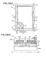
- Fig. 18 represents a plan view to show a pixel unit PXL of a display panel PNL shown in Fig. 17 and a cross-sectional view to explain an arrangement of a thin-film transistor TFT to make up the pixel unit PXL.
- Fig. 18 (a) is a plan view of a pixel unit PXL arranged in matrix-like form as shown in Fig. 17
- Fig. 18(b) is a cross-sectional view of the thin-film transistor TFT in the pixel unit PXL along the line A-A'.
- the thin-film transistor TFT is disposed at an intersection of the gate line GL and the data line DL. Also, a pixel electrode PX is connected to the thin-film transistor TFT, and an auxiliary capacity is formed with the auxiliary capacity line CL.
- a gate electrode GT and a gate insulator GI to cover the gate electrode GT are prepared on an insulating substrate SUB1.
- a silicon (Si) semiconductor layer SI, an ohmic contact layer (n + Si) NS, a source electrode SD1 and a drain electrode SD2 are sequentially laminated on the insulator.
- silicon nitride (SiNx) is deposited to cover the gate line GL and the gate electrode GT, and a plurality of data lines DL are prepared to intersect the gate lines GL.
- the source electrode SD1 and the drain electrode SD2 are formed on the same layer.
- a unit pixel comprising a pixel unit PXL is provided.
- This unit pixel has a subpixel of a single color (red, green, or blue) in case of full-color display.
- the unit pixel is also simply referred as "pixel".
- the thin-film transistor (TFT) to make up the pixel unit PXL comprises, as described above, a gate electrode, a silicon semiconductor film prepared by patterning on the gate electrode, an ohmic contact layer (n + silicon) separately formed on upper layer of the silicon semiconductor film, and a source electrode and a drain electrode connected respectively to the separated ohmic contact layer.
- a protective layer PAS is deposited on the upper layer of the thin-film transistor.
- a pixel electrode PX - preferably made of ITO, is prepared by patterning, and it is connected to the source electrode (or to the drain electrode) SD1 via a contact hole provided in the protective film PAS.
- An orientation film (not shown) is deposited to cover the pixel electrode PX.
- a counter electrode in Fig. 17 (b) is prepared via a smooth layer (overcoat layer) and a 3-color filter (in case of full-color display).
- An orientation film is deposited to cover the counter electrode.
- An active matrix substrate i.e. one of the substrates as described above is superimposed on it, and a liquid crystal is sealed in a gap therebetween.
- the Patented Reference 1 as given below discloses a method for manufacturing lines of the active matrix substrate as described above by means of ink jet coating method.
- the gate electrode of the thin-film transistor TFT is prepared by ink jet coating method using a liquid containing a conductive material.
- a source electrode and a drain electrode of the thin-film transistor are prepared by ink jet coating method using a liquid containing a semiconductor material.
- the gate insulator to be formed on the active matrix substrate of the liquid crystal display panel is provided to insulate the gate line and data line.
- cross capacity at the intersection with the data line is increased, and this results in the delay of signal.
- the counter capacity between the gate line and the counter electrode is also increased. If the gate insulator is designed thicker to reduce the cross capacity and counter capacity, performance of the thin-film transistor are decreased as described above.
- US-A-2005/0095356 describes a liquid crystal display device having a plurality of gate and data lines, which lines intersect via an intermediate insulating layer. That layer covers the gate line and a gate electrode of a thin film transistor extending from the gate lime to a region enclosed by the gate and data lines.
- EP-A-0 750 350 describes a solid state array device having a plurality of pixels with respective thin film transistor switches and a manufacturing method therefor. A plurality of first address lines are arranged perpendicular to a plurality of second address lines.
- a TFT gate dielectric layer is disposed over the first address lines, and a crossover region supplemental dielectric layer is disposed in respective ones of the crossover regions between the first and second address lines.
- US-A-5,365,079 describes a liquid crystal display panel and a manufacturing method therefor, the liquid crystal display panel including an additional insulating layer formed between crossing orthogonal source lines and gate lines to provide a higher breakdown voltage between the source lines and gate lines than at the gate insulating layer of the thin film transistors.
- JP-A-09-045774 describes a film semiconductor device wherein a film transistor and wiring part are stacked on an insulating substrate.
- the wiring part has a lower wiring and an upper wiring patterned on the insulating substrate, and a composite insulating pad interposed at least in the crossing of both wirings.
- the composite insulating pad contains a lower insulating film, a middle semiconductor film, and an upper insulating film.
- another insulator may be provided by applying a further insulator layer with low dielectric constant on an upper or lower surface of the gate insulator layer, locally formed at the intersections of said gate line and said data lines, the peripheral edges of said further insulator layer on each side of each gate line having a tapered form with a gentle slope in cross sectional view, and performance characteristics of the thin-film transistor is improved without increasing cross capacity at the intersection and a capacity from the counter electrode (counter capacity)
- a further insulating material with low dielectric constant may be dropped by ink jet coating-method along the gate line including an intersection with the data line to an upper layer or to a lower layer of a gate insulator to cover the gate line, peripheral edges of said further insulating material with low dielectric constant on each side of each gate line being turned into tapered form with a gentle slope in cross sectional view.
- the source electrode, and the drain electrode After the formation of the data lines, the source electrode, and the drain electrode, a silicon semiconductor layer is deposited and a semiconductor island is prepared by patterning. Then, the thin-film transistor is provided by preparing an ohmic conduct layer, the source electrode, and the drain electrode. After the formation of a protective film, a pixel electrode connected to the source electrode (or drain electrode) of the thin-film transistor is prepared via a contact hole opened in the protective film. Then, the liquid crystal display panel is prepared by a process already known, and the liquid crystal display device can be provided.
- the present invention it is possible to provide coating of an insulating material with low dielectric constant to the extent as necessary only on the intersection of the gate line and the data line or on the gate line including the intersection and to an upper layer or to a lower layer of the gate insulator.
- an insulating material with low dielectric constant to the extent as necessary only on the intersection of the gate line and the data line or on the gate line including the intersection and to an upper layer or to a lower layer of the gate insulator.
- Fig. 1 represents plan views to explain essential processes of a method for manufacturing an active matrix substrate of a liquid crystal display panel, which constitutes Embodiment 1 of the liquid crystal display device according to the present invention.
- description will be given on processes to form data lines and source electrodes and drain electrodes in the processes (1) to (4).
- a gate line GL is prepared by patterning on surface of an insulating substrate - preferably a transparent glass substrate.
- a gate electrode GT of a thin-film transistor is provided to protrude on it.
- Fig. 2 is a cross-sectional view of the active matrix substrate along the line A-A when the data line is prepared in the process (4) shown in Fig. 1 .
- a gate line GL is formed on surface of a glass substrate SUB1.
- the gate insulator GI is formed over the entire surface of the glass substrate SUB1 to cover the gate line GL.
- an ink of an insulating material with low dielectric constant such as an aromatic hydrocarbon type organic polymer and polyallyl ether type organic polymer is dropped by ink jet coating method. When this ink is dried up, it is turned to the insulator LDP with low dielectric constant.
- the data lines DL are provided to cross.
- peripheral edge of the insulator LDP with low dielectric constant dropped by ink jet coating method and hardened is turned to a tapered form with gentle slope in cross sectional view.
- the data line DL crossing the gate line GL runs over the gate line GL with gentle slope in cross sectional view and this prevents breaking of lines caused by skip-over.
- a counter electrode on a color filter substrate there is no dielectric substance, which narrows down the distance between electrodes except the above-mentioned crossing portion.
- Embodiment 1 it is possible to improve performance characteristics of the thin-film transistor without increasing cross capacity and counter capacity and to provide a liquid crystal display device to be operated at high speed and with high precision.
- Fig. 3 represents plan views to explain essential processes of a method for manufacturing an active matrix substrate of a liquid crystal display panel, which makes up Embodiment 2 of the liquid crystal display device according to the present invention.
- the processes to prepare the data line, the source electrode and drain electrode are described in the order of (1) to (4).
- the processes to prepare the data line, the source electrode and drain electrode are described in the order of (1) to (4).
- the processes to prepare the data line, the source electrode and drain electrode are described in the order of (1) to (4).
- a gate line GL is prepared by patterning on the surface of an insulating substrate - preferably a transparent glass substrate.
- a gate electrode GT of the thin-film transistor is prepared to protrude.
- Fig. 4 is a cross-sectional view of the active matrix substrate along the line A-A with the data line prepared in the process (4) of Fig. 3 .
- the gate line GL is formed on the surface of a glass substrate SUB1.
- an ink of an insulating material with low dielectric constant such as aromatic hydrocarbon type organic polymer or polyallyl ether type organic polymer is dropped and coated by ink jet coating.
- the ink is dried up, it is turned to an insulator LDP with low dielectric constant.
- a gate insulator GI is formed over the entire surface of the glass substrate SUB1 to cover the gate line GL, which has the insulator LDP with low dielectric constant at the intersection.
- a data line DL is disposed on a 2-layer insulating structure, which comprises the insulator LDP with low dielectric constant and the gate insulator GI.
- peripheral edge of the insulator LDP with low dielectric constant prepared by ink jet coating and hardened is turned to a tapered form with gentle slope. It forms an edge more gently tapered than the gate insulator GI on it.
- the data line DL intersecting with the gate line GL goes over the gate line GL at a gentle angle in cross sectional view.
- disconnection can be avoided, which may be caused by skip-over when jumping at a steep angle.
- Between the data line DL and a counter electrode of a color filter substrate (not shown), there is no dielectric substance, which narrows down the distance between electrodes.
- Embodiment 2 it is possible to improve performance characteristics of the thin-film transistor without increasing cross capacity and counter capacity and to provide a liquid crystal display device to be operated at high speed and with high precision.
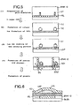
- Fig. 5 represents plan views to explain essential processes of a method for manufacturing an active matrix substrate of a liquid crystal display panel, which makes up Embodiment 3 of the liquid crystal display device according to the present invention.
- the gate line and the data line are also prepared by ink jet coating. Description will be given now on the processes to prepare the data line, the source electrode and drain electrode in the order of (1) to (4).
- (1) Preparation of the gate electrode A gate line and a bank BNK-G to form a groove on the pattern of the gate electrode are provided on the surface of an insulating substrate - preferably a transparent glass substrate.
- the bank BNK-G and its groove are prepared from a photosensitive resist by photolithographic method. This is the same in the other embodiments.
- An ink containing conductive particles such as silver or copper is dropped into the groove of the bank BNK-G by ink jet coating and the groove is filled.
- the gate line GL and the gate electrode GT are prepared by baking.
- Fig. 6 is a cross-sectional view of an active matrix substrate along the line A-A with the data line prepared in the process (4) of Fig. 5 .
- the gate line GL is prepared in the groove of the bank BNK-G formed on the surface of a glass substrate SUB1.
- a gate insulator GI is prepared over the entire surface of the glass substrate SUB1 to cover the gate line GL.
- an ink of an insulating material with low dielectric constant such as aromatic hydrocarbon type organic polymer or polyallyl ether type organic polymer is dropped by ink jet coating on the gate line GL and on the gate line GL on a portion where the data line intersects. When this ink is dried up, it is turned to an insulator LDP with low dielectric constant.
- the data line DL is prepared to cross it.
- the gate insulator GI is formed flatly on the bank BNK-G.
- Peripheral edge of the insulator LD with low dielectric constant prepared by ink jet coating and hardened is formed in a tapered form with gentle slope in cross sectional view.
- Embodiment 3 it is possible to improve performance characteristics of the thin-film transistor without increasing cross capacity and counter capacity and to provide a liquid crystal display device to be operated at high speed and with high precision.
- Fig. 7 represents plan views to explain essential processes of a method for manufacturing an active matrix substrate of a liquid crystal display panel, which makes up Embodiment 4 of the liquid crystal display device of the present invention.
- the gate line and data line are prepared in Embodiment 4 by ink jet coating method.
- description will be given on the process to prepare the data line, the source electrode and the drain electrode in the order of (1) to (4).
- (1) Preparation of gate electrode On the surface of an insulating substrate - preferably a transparent glass substrate, a gate line and a bank BNK-G to form a groove on the pattern of the gate line and gate electrode are provided. An ink containing conductive particles such as silver or copper is dropped into the groove of the bank BNK-G to fill it. Then, this is dried up, and a gate line GL and a gate electrode GT are prepared by baking.
- Fig. 8 is a cross-sectional view of an active matrix substrate along the line A-A with the data line prepared in the process (4) of Fig. 7 .
- a gate line GL is prepared in the groove of the bank BNK-G formed on the surface of the glass substrate SUB1.
- an ink of an insulating material with low dielectric constant such as aromatic hydrocarbon type organic polymer, polyallyl ether type organic polymer, etc. is dropped by ink jet coating. When this ink is dried up, it is turned to an insulator LDP with low dielectric constant.
- the gate insulator GI is prepared over the entire surface of the glass substrate SUB1 to cover the insulator LDP with low dielectric constant.
- the data lines DL are formed to cross.
- peripheral edge is prepared having a tapered form with a gentle slope in cross sectional view because of the bank 8NK-G
- disconnection can be avoided, which may be caused by skip-over when the data line.DL crossing the gate line GL goes with gentle slope in cross sectional view over the gate line GL.
- a counter electrode of a color filter substrate not shown
- Embodiment 4 it is possible to improve performance characteristics of the thin-film transistor without increasing cross capacity and counter capacity and to provide a liquid crystal display device to be operated at high speed and with high precision.
- Fig. 9 represents plan views to explain essential processes of a method for manufacturing an active matrix substrate of a liquid crystal display panel, which makes up Embodiment 5 of the liquid crystal display device of the present invention.
- description will be given on the processes to prepare the data line, the source electrode, and the drain electrode in the order of (1) to (4).
- a gate line GL is prepared by patterning on the surface of an insulating substrate - preferably a transparent glass substrate.
- a gate electrode GT of the thin-film transistor is prepared to protrude.
- Fig. 10 is a cross-sectional view of an active matrix substrate along the line B-B with the data line prepared in the process (4) of Fig. 9 , and a liquid crystal is sealed by attaching another substrate on it.
- a gate line GL is prepared on the surface of the glass substrate SUB1, which makes up the active matrix substrate.
- the gate insulator GI is formed on the entire surface of the glass substrate SUB1 to cover the gate line GL.
- an ink of an insulating material with low dielectric constant such as aromatic hydrocarbon type organic polymer, polyallyl ether type organic polymer, etc. is dropped by ink jet coating. When this ink is dried up, it is turned to an insulator LDP with low dielectric constant on the insulator GI along the gate line GL.
- the data line DL is prepared to cross.
- peripheral edge of the insulator LDF with low dielectric constant is formed in a tapered form with gentle slope in cross sectional view.
- disconnection can be avoided, which may be caused by skip-over when the data line DL crossing the gate line GL goes over the gate line GL at a steep angle.
- a counter electrode CT of the color filter substrate SUB2 there is no dielectric substance, which narrows down the distance between electrodes except the portion of the gate line GL including the intersection as described above.
- a liquid crystal LC is sealed between an orientation film ORI1 on the active matrix substrate SUB1 and an orientation film ORI2 on the color filter substrate SUB2.
- Embodiment 5 cross capacity and counter capacity are not increased. Between the signal lines such as data line and the counter electrode, there is only an insulator LDP with low dielectric constant on the gate line GL as a dielectric substance to narrow down the distance between electrodes, and it is not a structure to extensively increase the capacity. For this reason, it is possible to provide a liquid crystal display device to be operated at high speed and with high precision without decreasing the performance characteristics of the thin-film transistor.
- Fig. 11 represents plan views to explain essential processes of a method for manufacturing an active matrix substrate of a liquid crystal display panel, which makes up Embodiment 6 of the liquid crystal display device of the present invention.
- description will be given on the processes to prepare the data line, the source electrode, and the drain electrode in the order of (1) to (4).
- a gate line GL is prepared by patterning on the surface of an insulating substrate - preferably a transparent glass substrate.
- a gate electrode GT of the thin-film transistor is formed to protrude.
- Fig. 12 is a cross-sectional view of an active matrix substrate along the line B-B with the data line prepared in the process (4) of Fig. 11 , and a liquid crystal is sealed by attaching another substrate.
- the gate line GL is prepared on the surface of the glass substrate SUB1, which makes up the active matrix substrate.
- An insulator LDP with low dielectric constant is prepared on the gate line GL including a portion where data line crosses and a gate insulator GI is prepared on it.
- an ink of an insulating material with low dielectric constant such as aromatic hydrocarbon type organic polymer, polyallyl ether type organic polymer, etc. is dropped by ink jet coating method. When it is dried up, it is turned to an insulator LDP with low dielectric constant on the gate insulator GI along the gate line GL.
- the data line DL is prepared to cross.
- peripheral edge of the insulator LDP with low dielectric constant is prepared in a tapered form with gentle in cross sectional view.
- the data line DL crossing the gate line GL goes over the gate line GL at gentle slope in cross sectional view, and disconnection can be avoided, which may be caused by skip-over when jumping at a steep angle.
- a liquid crystal LC is sealed between an orientation film ORI1 on the active matrix substrate SUB1 and an orientation film ORI2 on the color filter substrate SUB2.
- Embodiment 6 cross capacity and counter capacity are not increased. Between the signal lines such as data line and the counter electrode, there is only an insulator LDP with low dielectric constant on the gate line as a dielectric substance to narrow down the distance between electrodes, and it is not a structure to extensively increase the capacity. For this reason, it is possible to provide a liquid crystal display device to be operated at high speed and with high precision without decreasing the performance characteristics of the thin-film transistor.
- Fig. 13 represents plan views to explain essential processes of a method for manufacturing an active matrix substrate of a liquid crystal display panel, which makes up Embodiment 7 of the liquid crystal display device of the present invention.
- description will be given on the processes to prepare the data line, the source electrode and the drain electrode in the order of (1) to (4).
- Fig. 14 is a cross-sectional view of an active-matrix substrate along the line B-B with data line prepared in the process (4) of Fig. 13 , and the liquid crystal is sealed by attaching another substrate.
- a gate line GL is prepared on the entire surface of the glass substrate SUB1, which constitutes the active matrix substrate.
- a gate insulator GI is prepared over the entire surface of the glass substrate SUB1 to cover the gate line GL.
- the gate insulator GI is prepared in flat form because of the presence of the bank BNK-G.
- an ink of an insulating material with low dielectric constant such as aromatic hydrocarbon type organic polymer, polyallyl ether type organic polymer, etc. is dropped by ink jet coating.
- the ink is dried up, it is turned to an insulator LDP with low dielectric constant on the gate insulator GI along the gate line GL.
- a data line DL is prepared to cross.
- peripheral edge of the insulator LD with low dielectric constant is formed in a tapered form with gentle slope in cross sectional view.
- the data line DL crossing the gate line GL goes over the gate line GL with gentle slope in cross sectional view, and disconnection can be avoided, which may be caused by skip-over when jumping at a steep angle.
- a liquid crystal LC is sealed between an orientation film ORI1 on the active matrix substrate SUB1 and an orientation film ORI2 on the color filter substrate SUB2.
- Embodiment 7 cross capacity and counter capacity are not increased. Between the signal lines such as data line and the counter electrode, there is only an insulator LDP with low dielectric constant on the gate line as a dielectric substance to narrow down the distance between electrodes, and it is not a structure to extensively increase the capacity. For this reason, it is possible to provide a liquid crystal display device to be operated at high speed and with high precision without decreasing the performance characteristics of the thin-film transistor.
- Fig. 15 represents plan views to explain essential processes of a method for manufacturing an active matrix substrate of a liquid crystal display panel, which makes up Embodiment 8 of the liquid crystal display device of the present invention.
- description will be given on the processes to prepare the data line, the source electrode and the drain electrode in the order of (1) to (4).
- Fig. 16 is a cross-sectional view of an active matrix substrate along the line B-B with data line prepared in the process (4) of Fig. 15 with the liquid crystal sealed by attaching another substrate.
- a gate line GL is prepared on the surface of the glass substrate SUB1, which makes up the active matrix substrate.
- an ink of an insulating material with low dielectric constant such as aromatic hydrocarbon type organic polymer, polyallyl ether type organic polymer, etc. is dropped by ink jet coating method.
- the ink is dried up, it is turned to an insulator LDP with low dielectric constant on the gate insulator GI along the gate line GL.
- a gate insulator GI is prepared on it.
- the gate insulator GI is prepared in flat form because of the presence of the bank BNK-G.
- the data line DL is prepared to cross.
- peripheral edge of the insulator LDP with low dielectric constant is formed in a tapered form with gentle slope in cross sectional view.
- the data line intersecting the gate line GL goes over the gate line GL at a gentle angle in cross sectional view, and disconnection can be avoided, which may be caused by skip-over when jumping at a steep angle.
- a liquid crystal LC is sealed between an orientation film ORI1 on the active matrix substrate SUB1 and an orientation film ORI2 on the color filter substrate SUB2.
- Embodiment 8 cross capacity and counter capacity are not increased. Between the signal lines such as data line and the counter electrode, there is only an insulator LDP with low dielectric constant on the gate line as a dielectric substance to narrow down the distance between electrodes, and it is not a structure to extensively increase the capacity. For this reason, it is possible to provide a liquid crystal display device to be operated at high speed and with high precision without decreasing the performance characteristics of the thin-film transistor.
Landscapes
- Physics & Mathematics (AREA)
- Nonlinear Science (AREA)
- Engineering & Computer Science (AREA)
- Microelectronics & Electronic Packaging (AREA)
- Mathematical Physics (AREA)
- Chemical & Material Sciences (AREA)
- Crystallography & Structural Chemistry (AREA)
- General Physics & Mathematics (AREA)
- Optics & Photonics (AREA)
- Liquid Crystal (AREA)
- Internal Circuitry In Semiconductor Integrated Circuit Devices (AREA)
- Thin Film Transistor (AREA)
Claims (10)
- Flüssigkristallanzeigevorrichtung mit einer Flüssigkristall- (LC-) Schicht, die zwischen einem ersten isolierenden Substrat (SUB1) und einem zweiten isolierenden Substrat (SUB2) angeordnet ist, worin die Flüssigkristallanzeigevorrichtung Folgendes umfasst:eine Vielzahl an Gate-Leitungen (GL), die parallel zu einander hergestellt und auf dem ersten isolierenden Substrat (SUB1) angeordnet sind;eine Vielzahl an Datenleitungen (DL), die parallel zu einander hergestellt und auf dem ersten isolierenden Substrat (SUB1) so angeordnet sind, dass sie die Gate-Leitungen (GL) über eine Gate-Isolationsschicht (GI) hinweg schneiden;wobei jeder der durch die Gate-Leitungen (GL) und Datenleitungen (DL) eingeschlossenen Bereiche als Einheitspixelbereich (PXL) definiert ist und ein Bereich, in dem die Vielzahl an Gate-Leitungen (GL) und die Vielzahl an Datenleitungen (DL) einander kreuzen, einen Anzeigebereich (PNL) bildet;
wobei die Flüssigkristallanzeigevorrichtung ferner Folgendes umfasst: eine Vielzahl an Dünnschichtransistoren, die jeweils aus einer Gate-Elektrode (GT) bestehen, die sich von jeweils einer Gate-Leitung (GL) zu dem Einheitspixelbereich erstreckt, wobei die Gate-Isolationsschicht (GI) die Gate-Leitung (GL) und die Gate-Elektrode (GT) abdeckt; eine Halbleiterschicht (SI), die sequenziell auf der Gate-Isolationsschicht (GI) hergestellt ist; eine ohmsche Kontaktschicht (NS), die separat auf der Oberfläche der Halbleiterschicht (SI) hergestellt ist; und eine Source-Elektrode (SD1) und eine Drain-Elektrode (SD2), die auf der separaten ohmschen Kontaktschicht (NS) ausgebildet sind;
dadurch gekennzeichnet, dass die Flüssigkristallanzeigevorrichtung eine weitere Isolationsschicht (LDP) mit niedriger Dielektrizitätskonstante auf einer oberen oder unteren Oberfläche der Gate-Isolationsschicht (GI) umfasst, die lokal an den Schnittpunkten der Gate-Leitungen (GL) und der Datenleitungen (DL) ausgebildet ist,
wobei die am Rand gelegenen Kanten der weiteren Isolationsschicht (LDP) auf jeder Seite jeder Gate-Leitung (GL) eine angeschrägte Form mit einem in der Querschnittsansicht flachen Anstieg aufweisen. - Flüssigkristallanzeigevorrichtung nach Anspruch 1, worin die weitere Isolationsschicht (LDP) zusätzlich zu allen Schnittpunkten entlang der Gate-Leitungen (GL) bereitgestellt ist.
- Flüssigkristallanzeigevorrichtung nach Anspruch 1 oder 2, worin die weitere Isolationsschicht (LDP) aus einem wärmebeständigen Harz ausgebildet ist.
- Flüssigkristallanzeigevorrichtung nach Anspruch 1 oder 2, worin die weitere Isolationsschicht (LDP) aus einem organischen Polymer vom aromatischen Kohlenwasserstofftyp oder einem organischen Polymer vom Polyallylethertyp ausgebildet ist.
- Verfahren zur Herstellung einer Flüssigkristallanzeigevorrichtung mit einer Flüssigkristallschicht (LC), die zwischen einem ersten isolierenden Substrat (SUB1) und einem zweiten isolierenden Substrat (SUB2) angeordnet ist, wobei das Verfahren folgende Schritte umfasst:Herstellen einer Vielzahl an Gate-Leitungen (GL), die parallel zueinander verlaufen, auf dem ersten isolierenden Substrat (SUB1);Abscheiden einer Gate-Isolationsschicht (GI) zum Abdecken des ersten isolierenden Substrats (SUB1) und der Gate-Leitungen (GL);lokales Herstellen einer weiteren Isolationsschicht mit niedriger Dielektrizitätskonstante (LDP) auf der Gate-Isolationsschicht (GI) auf Abschnitten der Gate-Leitungen (GL); undHerstellen einer Vielzahl an Datenleitungen (DL), die parallel zueinander verlaufen und die Gate-Leitungen (GL) auf der Gate-Isolationsschicht (GI) und der weiteren Isolationsschicht (LDP) auf den zuvor genannten Abschnitten kreuzen,dadurch gekennzeichnet, dass die Isolationsschicht mit niedriger Dielektrizitätskonstante (LDP) durch Tintenstrahlbeschichtung hergestellt wird, wobei die am Rand gelegenen Kanten der Isolationsschicht mit niedriger Dielektrizitätskonstante (LDP) auf jeder Seite der Gate-Leitungen (GL) in eine angeschrägte Form gebracht werden, wobei sie in der Querschnittsansicht einen flachen Anstieg aufweisen.
- Verfahren zur Herstellung einer Flüssigkristallanzeigevorrichtung mit einer Flüssigkristallschicht (LC), die zwischen einem ersten isolierenden Substrat (SUB1) und einem zweiten isolierenden Substrat (SUB2) angeordnet ist, wobei das Verfahren folgende Schritte umfasst:Herstellen einer Vielzahl an Gate-Leitungen (GL), die parallel zueinander verlaufen, auf dem ersten isolierenden Substrat (SUB1);lokales Herstellen einer Isolationsschicht (LDP) mit niedriger Dielektrizitätskonstante auf den Gate-Leitungen (GL) auf Abschnitten der Gate-Leitungen (GL);Abscheiden einer Gate-Isolationsschicht (GI) zur Abdeckung des ersten Isolationssubstrats (SUB1), der Gate-Leitungen (GL) und der Isolationsschicht (LDP) mit niedriger Dielektrizitätskonstante; undHerstellen einer Vielzahl an Datenleitungen (DL), die parallel zueinander verlaufen und die Gate-Leitungen (GL) auf der Isolationsschicht (LDP) mit niedriger Dielektrizitätskonstante und der Gate-Isolationsschicht (GI) auf den zuvor genannten Abschnitten kreuzen, dadurch gekennzeichnet, dass die Isolationsschicht (LDP) mit niedriger Dielektrizitätskonstante durch Tintenstrahlbeschichtung ausgebildet wird, wobei die am Rand gelegenen Kanten der Isolationsschicht (LDP) mit niedriger Dielektrizitätskonstante auf jeder Seite der Gate-Leitungen (GL) in eine angeschrägte Form gebracht werden, wobei sie in der Querschnittsansicht einen flachen Anstieg aufweisen.
- Verfahren nach Anspruch 5 oder 6, worin die weitere Isolationsschicht (LDP) mit niedriger Dielektrizitätskonstante entlang aller Gate-Leitungen (GL) hergestellt wird.
- Verfahren zur Herstellung einer Flüssigkristallanzeigevorrichtung nach einem der Ansprüche 5 bis 7, wobei das Verfahren ferner folgenden Schritt umfasst:Herstellen eines Dünnschichttransistors, wobei der Dünnschichtransistor eine Halbleiterschicht (SI) auf der Gate-Isolationsschicht (GI) und eine separat bereitgestellte ohmsche Kontaktschicht (NS) auf einer Oberfläche der Halbleiterschicht (SI) aufweist, wobei eine Source-Elektrode (SD1) und eine Drain-Elektrode (SD2) auf der separaten ohmschen Kontaktschicht (NS) hergestellt sind; und ein Anzeigebereich (DNL) aus Einheitspixelbereichen (PXL) ausgebildet wird, die auf jedem durch die Vielzahl an Gate-Leitungen (GL) und die Vielzahl an Datenleitungen (DL) umschlossenen Abschnitten auszubilden sind.
- Verfahren zur Herstellung einer Flüssigkristallanzeigevorrichtung nach einem der Ansprüche 5 bis 8, worin die weitere Isolationsschicht mit niedriger Dielektrizitätskonstante (LDP) aus einem wärmebeständigen Harz ausgebildet ist.
- Verfahren zur Herstellung einer Flüssigkristallanzeigevorrichtung nach einem der Ansprüche 5 bis 8, worin die weitere Isolationsschicht (LDP) aus einem organischen Polymer vom aromatischen Kohlenwasserstofftyp oder einem organischen Polymer vom Polyallylethertyp ausgebildet ist.
Applications Claiming Priority (1)
| Application Number | Priority Date | Filing Date | Title |
|---|---|---|---|
| JP2005365739A JP4395659B2 (ja) | 2005-12-20 | 2005-12-20 | 液晶表示装置とその製造方法 |
Publications (2)
| Publication Number | Publication Date |
|---|---|
| EP1801640A1 EP1801640A1 (de) | 2007-06-27 |
| EP1801640B1 true EP1801640B1 (de) | 2009-09-09 |
Family
ID=37834122
Family Applications (1)
| Application Number | Title | Priority Date | Filing Date |
|---|---|---|---|
| EP06256296A Not-in-force EP1801640B1 (de) | 2005-12-20 | 2006-12-11 | Flüssigkristallanzeigevorrichtung und Methode zu ihrer Herstellung |
Country Status (7)
| Country | Link |
|---|---|
| US (2) | US7816158B2 (de) |
| EP (1) | EP1801640B1 (de) |
| JP (1) | JP4395659B2 (de) |
| KR (2) | KR100845406B1 (de) |
| CN (1) | CN1987572B (de) |
| DE (1) | DE602006009059D1 (de) |
| TW (1) | TWI317557B (de) |
Families Citing this family (15)
| Publication number | Priority date | Publication date | Assignee | Title |
|---|---|---|---|---|
| JP4395659B2 (ja) * | 2005-12-20 | 2010-01-13 | 株式会社フューチャービジョン | 液晶表示装置とその製造方法 |
| JP4297505B2 (ja) * | 2006-07-28 | 2009-07-15 | 株式会社フューチャービジョン | 液晶表示装置 |
| JP4565573B2 (ja) * | 2006-09-07 | 2010-10-20 | 株式会社フューチャービジョン | 液晶表示パネルの製造方法 |
| CN100595927C (zh) * | 2007-07-05 | 2010-03-24 | 胜华科技股份有限公司 | 主动元件阵列基板及液晶显示面板 |
| US9041202B2 (en) | 2008-05-16 | 2015-05-26 | Semiconductor Energy Laboratory Co., Ltd. | Semiconductor device and manufacturing method of the same |
| KR101525805B1 (ko) | 2008-06-11 | 2015-06-05 | 삼성디스플레이 주식회사 | 표시 장치 및 그 제조 방법 |
| JP5442228B2 (ja) * | 2008-08-07 | 2014-03-12 | 株式会社ジャパンディスプレイ | 表示装置及び表示装置の製造方法 |
| JP5202254B2 (ja) | 2008-11-27 | 2013-06-05 | 株式会社ジャパンディスプレイイースト | 表示装置および表示装置の製造方法 |
| US8114720B2 (en) * | 2008-12-25 | 2012-02-14 | Semiconductor Energy Laboratory Co., Ltd. | Semiconductor device and manufacturing method thereof |
| JP5397175B2 (ja) * | 2009-11-13 | 2014-01-22 | セイコーエプソン株式会社 | 半導体装置用基板及びその製造方法、半導体装置並びに電子機器 |
| US9018704B2 (en) | 2011-10-20 | 2015-04-28 | Panasonic Corporation | Thin-film transistor and method of manufacturing the same |
| GB2498072B (en) * | 2011-12-21 | 2015-03-18 | Lg Display Co Ltd | Display device and method for manufacturing of the same |
| US9318320B2 (en) | 2012-10-26 | 2016-04-19 | Sharp Kabushiki Kaisha | Production method for active element substrate, active element substrate, and display device |
| CN103487961B (zh) * | 2013-10-22 | 2016-01-06 | 合肥京东方光电科技有限公司 | 显示面板检测方法 |
| JP6160507B2 (ja) * | 2014-02-25 | 2017-07-12 | 富士ゼロックス株式会社 | レンズアレイ及びレンズアレイ製造方法 |
Family Cites Families (16)
| Publication number | Priority date | Publication date | Assignee | Title |
|---|---|---|---|---|
| US5365079A (en) * | 1982-04-30 | 1994-11-15 | Seiko Epson Corporation | Thin film transistor and display device including same |
| TW241310B (de) | 1992-07-11 | 1995-02-21 | Man GutehoffnungshTe Aktiengesellschaft | |
| US5631473A (en) | 1995-06-21 | 1997-05-20 | General Electric Company | Solid state array with supplemental dielectric layer crossover structure |
| JPH0945774A (ja) | 1995-07-28 | 1997-02-14 | Sony Corp | 薄膜半導体装置 |
| US6613650B1 (en) * | 1995-07-31 | 2003-09-02 | Hyundai Electronics America | Active matrix ESD protection and testing scheme |
| JP2000133649A (ja) | 1998-10-22 | 2000-05-12 | Canon Inc | 素子回路基板上の絶縁膜の形成方法 |
| KR20010063291A (ko) * | 1999-12-22 | 2001-07-09 | 박종섭 | 박막 트랜지스터 액정표시소자 |
| KR20030073006A (ko) * | 2002-03-08 | 2003-09-19 | 삼성전자주식회사 | 저유전율 절연막을 사용하는 박막 트랜지스터 기판 및 그제조 방법 |
| KR100853220B1 (ko) | 2002-04-04 | 2008-08-20 | 삼성전자주식회사 | 표시 장치용 박막 트랜지스터 어레이 기판의 제조 방법 |
| JP2003318193A (ja) | 2002-04-22 | 2003-11-07 | Seiko Epson Corp | デバイス、その製造方法及び電子装置 |
| WO2004086487A1 (ja) | 2003-03-26 | 2004-10-07 | Semiconductor Energy Laboratory Co. Ltd. | 半導体装置およびその作製方法 |
| JP3923462B2 (ja) * | 2003-10-02 | 2007-05-30 | 株式会社半導体エネルギー研究所 | 薄膜トランジスタの作製方法 |
| US7372513B2 (en) * | 2003-12-30 | 2008-05-13 | Lg.Philips Lcd Co., Ltd. | Liquid crystal display device and method for fabricating the same |
| JP2005227538A (ja) | 2004-02-13 | 2005-08-25 | Chi Mei Electronics Corp | 大画面および高精細のディスプレイに対応したアレイ基板およびその製造方法 |
| US8058652B2 (en) * | 2004-10-28 | 2011-11-15 | Semiconductor Energy Laboratory Co., Ltd. | Semiconductor device used as electro-optical device having channel formation region containing first element, and source or drain region containing second element |
| JP4395659B2 (ja) * | 2005-12-20 | 2010-01-13 | 株式会社フューチャービジョン | 液晶表示装置とその製造方法 |
-
2005
- 2005-12-20 JP JP2005365739A patent/JP4395659B2/ja not_active Expired - Fee Related
-
2006
- 2006-02-09 KR KR1020060012394A patent/KR100845406B1/ko not_active Expired - Fee Related
- 2006-02-10 CN CN2006100793668A patent/CN1987572B/zh not_active Expired - Fee Related
- 2006-02-21 TW TW095105779A patent/TWI317557B/zh not_active IP Right Cessation
- 2006-06-15 US US11/452,978 patent/US7816158B2/en not_active Expired - Fee Related
- 2006-12-11 EP EP06256296A patent/EP1801640B1/de not_active Not-in-force
- 2006-12-11 DE DE602006009059T patent/DE602006009059D1/de active Active
-
2008
- 2008-05-06 KR KR1020080041883A patent/KR100961359B1/ko not_active Expired - Fee Related
-
2009
- 2009-02-11 US US12/369,220 patent/US7738048B2/en not_active Expired - Fee Related
Also Published As
| Publication number | Publication date |
|---|---|
| US7816158B2 (en) | 2010-10-19 |
| DE602006009059D1 (de) | 2009-10-22 |
| KR20070065761A (ko) | 2007-06-25 |
| TWI317557B (en) | 2009-11-21 |
| CN1987572B (zh) | 2010-10-13 |
| US7738048B2 (en) | 2010-06-15 |
| TW200725901A (en) | 2007-07-01 |
| KR20080045668A (ko) | 2008-05-23 |
| CN1987572A (zh) | 2007-06-27 |
| EP1801640A1 (de) | 2007-06-27 |
| KR100961359B1 (ko) | 2010-06-04 |
| KR100845406B1 (ko) | 2008-07-10 |
| US20070138469A1 (en) | 2007-06-21 |
| JP4395659B2 (ja) | 2010-01-13 |
| JP2007171314A (ja) | 2007-07-05 |
| US20090213289A1 (en) | 2009-08-27 |
Similar Documents
| Publication | Publication Date | Title |
|---|---|---|
| US7738048B2 (en) | Liquid crystal display device and method for manufacturing the same | |
| KR100333983B1 (ko) | 광시야각 액정 표시 장치용 박막 트랜지스터 어레이 기판 및그의 제조 방법 | |
| US8178878B2 (en) | Mother thin film transistor array substrate and thin film transistor array substrate fabricated therefrom | |
| US6927815B2 (en) | Thin film transistor liquid crystal display and method for manufacturing the same | |
| US7138655B2 (en) | Thin film transistor array panel including symmetrically aligned thin film transistors and manufacturing method thereof | |
| KR20060079040A (ko) | 프린지 필드 스위칭 타입의 박막 트랜지스터 기판 및 그제조 방법 | |
| KR20050042991A (ko) | 수평 전계 인가형 박막 트랜지스터 기판 및 그 제조 방법 | |
| US9761613B2 (en) | TFT array substrate and manufacturing method thereof | |
| KR101085142B1 (ko) | 수평 전계 박막 트랜지스터 기판 및 그 제조 방법 | |
| US5995174A (en) | Liquid crystal display apparatus with source/drain electrodes and pixel electrode formed by the same material | |
| KR20050042646A (ko) | 수평 전계 인가형 박막 트랜지스터 기판 및 그 제조 방법 | |
| US7847907B2 (en) | Display substrate, method of fabricating the same, and liquid crystal display device having the same | |
| US6876404B2 (en) | Liquid crystal display device and fabricating method thereof | |
| US20070085939A1 (en) | Thin film transistor substrate with improved inter-layer adhesion | |
| KR100538327B1 (ko) | 수평 전계 인가형 박막 트랜지스터 어레이 기판 및 그제조 방법 | |
| KR100922271B1 (ko) | 액정 표시 패널 및 그 제조 방법 | |
| KR20010066244A (ko) | 액정 표시장치 제조방법 및 그 제조방법에 따른 액정표시장치 | |
| KR20080073573A (ko) | 액정패널과 이의 제조방법 | |
| KR20170083178A (ko) | 표시 장치 및 그 제조 방법 | |
| KR20050062692A (ko) | 액정표시장치 및 그 제조 방법 | |
| US8421939B2 (en) | Display control substrate, manufacturing method thereof, liquid crystal display panel, electronic information device | |
| KR100315922B1 (ko) | 4장의마스크를이용한액정표시장치용박막트랜지스터기판의제조방법및액정표시장치용박막트랜지스터기판 | |
| JP2000180890A (ja) | Tftアレイ基板及びこれを用いた液晶表示装置並びにtftアレイ基板の製造方法 | |
| KR20060061003A (ko) | 액정표시장치 | |
| KR20050068466A (ko) | 액정표시장치 및 그의 제조방법 |
Legal Events
| Date | Code | Title | Description |
|---|---|---|---|
| PUAI | Public reference made under article 153(3) epc to a published international application that has entered the european phase |
Free format text: ORIGINAL CODE: 0009012 |
|
| AK | Designated contracting states |
Kind code of ref document: A1 Designated state(s): AT BE BG CH CY CZ DE DK EE ES FI FR GB GR HU IE IS IT LI LT LU LV MC NL PL PT RO SE SI SK TR |
|
| AX | Request for extension of the european patent |
Extension state: AL BA HR MK YU |
|
| 17P | Request for examination filed |
Effective date: 20071030 |
|
| 17Q | First examination report despatched |
Effective date: 20071213 |
|
| AKX | Designation fees paid |
Designated state(s): DE FR GB |
|
| GRAP | Despatch of communication of intention to grant a patent |
Free format text: ORIGINAL CODE: EPIDOSNIGR1 |
|
| GRAS | Grant fee paid |
Free format text: ORIGINAL CODE: EPIDOSNIGR3 |
|
| GRAA | (expected) grant |
Free format text: ORIGINAL CODE: 0009210 |
|
| AK | Designated contracting states |
Kind code of ref document: B1 Designated state(s): DE FR GB |
|
| REG | Reference to a national code |
Ref country code: GB Ref legal event code: FG4D |
|
| REF | Corresponds to: |
Ref document number: 602006009059 Country of ref document: DE Date of ref document: 20091022 Kind code of ref document: P |
|
| PLBE | No opposition filed within time limit |
Free format text: ORIGINAL CODE: 0009261 |
|
| STAA | Information on the status of an ep patent application or granted ep patent |
Free format text: STATUS: NO OPPOSITION FILED WITHIN TIME LIMIT |
|
| 26N | No opposition filed |
Effective date: 20100610 |
|
| REG | Reference to a national code |
Ref country code: GB Ref legal event code: 732E Free format text: REGISTERED BETWEEN 20110714 AND 20110720 |
|
| REG | Reference to a national code |
Ref country code: DE Ref legal event code: R082 Ref document number: 602006009059 Country of ref document: DE Representative=s name: LEINWEBER & ZIMMERMANN, DE Effective date: 20110825 Ref country code: DE Ref legal event code: R081 Ref document number: 602006009059 Country of ref document: DE Owner name: SHARP K.K., JP Free format text: FORMER OWNER: FUTURE VISION INC., TOKYO, JP Effective date: 20110825 |
|
| REG | Reference to a national code |
Ref country code: FR Ref legal event code: TP Owner name: SHARP KABUSHIKI KAISHA, JP Effective date: 20110927 |
|
| PGFP | Annual fee paid to national office [announced via postgrant information from national office to epo] |
Ref country code: DE Payment date: 20121205 Year of fee payment: 7 |
|
| PGFP | Annual fee paid to national office [announced via postgrant information from national office to epo] |
Ref country code: GB Payment date: 20121205 Year of fee payment: 7 |
|
| PGFP | Annual fee paid to national office [announced via postgrant information from national office to epo] |
Ref country code: FR Payment date: 20130107 Year of fee payment: 7 |
|
| REG | Reference to a national code |
Ref country code: DE Ref legal event code: R119 Ref document number: 602006009059 Country of ref document: DE |
|
| GBPC | Gb: european patent ceased through non-payment of renewal fee |
Effective date: 20131211 |
|
| REG | Reference to a national code |
Ref country code: DE Ref legal event code: R119 Ref document number: 602006009059 Country of ref document: DE Effective date: 20140701 |
|
| REG | Reference to a national code |
Ref country code: FR Ref legal event code: ST Effective date: 20140829 |
|
| PG25 | Lapsed in a contracting state [announced via postgrant information from national office to epo] |
Ref country code: DE Free format text: LAPSE BECAUSE OF NON-PAYMENT OF DUE FEES Effective date: 20140701 |
|
| PG25 | Lapsed in a contracting state [announced via postgrant information from national office to epo] |
Ref country code: GB Free format text: LAPSE BECAUSE OF NON-PAYMENT OF DUE FEES Effective date: 20131211 Ref country code: FR Free format text: LAPSE BECAUSE OF NON-PAYMENT OF DUE FEES Effective date: 20131231 |