EP1771926B1 - Halbleiterlaserbauelement, optische vorrichtung für ein halbleiterlaserbauelement und verfahren zur herstellung einer optischen vorrichtung - Google Patents
Halbleiterlaserbauelement, optische vorrichtung für ein halbleiterlaserbauelement und verfahren zur herstellung einer optischen vorrichtung Download PDFInfo
- Publication number
- EP1771926B1 EP1771926B1 EP05759656.1A EP05759656A EP1771926B1 EP 1771926 B1 EP1771926 B1 EP 1771926B1 EP 05759656 A EP05759656 A EP 05759656A EP 1771926 B1 EP1771926 B1 EP 1771926B1
- Authority
- EP
- European Patent Office
- Prior art keywords
- semiconductor laser
- carrier
- radiation
- component according
- laser chip
- Prior art date
- Legal status (The legal status is an assumption and is not a legal conclusion. Google has not performed a legal analysis and makes no representation as to the accuracy of the status listed.)
- Ceased
Links
Images





Classifications
-
- H—ELECTRICITY
- H01—ELECTRIC ELEMENTS
- H01S—DEVICES USING THE PROCESS OF LIGHT AMPLIFICATION BY STIMULATED EMISSION OF RADIATION [LASER] TO AMPLIFY OR GENERATE LIGHT; DEVICES USING STIMULATED EMISSION OF ELECTROMAGNETIC RADIATION IN WAVE RANGES OTHER THAN OPTICAL
- H01S5/00—Semiconductor lasers
- H01S5/10—Construction or shape of the optical resonator, e.g. extended or external cavity, coupled cavities, bent-guide, varying width, thickness or composition of the active region
- H01S5/14—External cavity lasers
-
- H—ELECTRICITY
- H01—ELECTRIC ELEMENTS
- H01S—DEVICES USING THE PROCESS OF LIGHT AMPLIFICATION BY STIMULATED EMISSION OF RADIATION [LASER] TO AMPLIFY OR GENERATE LIGHT; DEVICES USING STIMULATED EMISSION OF ELECTROMAGNETIC RADIATION IN WAVE RANGES OTHER THAN OPTICAL
- H01S5/00—Semiconductor lasers
- H01S5/02—Structural details or components not essential to laser action
- H01S5/022—Mountings; Housings
- H01S5/023—Mount members, e.g. sub-mount members
- H01S5/02325—Mechanically integrated components on mount members or optical micro-benches
-
- H—ELECTRICITY
- H01—ELECTRIC ELEMENTS
- H01S—DEVICES USING THE PROCESS OF LIGHT AMPLIFICATION BY STIMULATED EMISSION OF RADIATION [LASER] TO AMPLIFY OR GENERATE LIGHT; DEVICES USING STIMULATED EMISSION OF ELECTROMAGNETIC RADIATION IN WAVE RANGES OTHER THAN OPTICAL
- H01S5/00—Semiconductor lasers
- H01S5/10—Construction or shape of the optical resonator, e.g. extended or external cavity, coupled cavities, bent-guide, varying width, thickness or composition of the active region
- H01S5/18—Surface-emitting [SE] lasers, e.g. having both horizontal and vertical cavities
- H01S5/183—Surface-emitting [SE] lasers, e.g. having both horizontal and vertical cavities having only vertical cavities, e.g. vertical cavity surface-emitting lasers [VCSEL]
-
- H—ELECTRICITY
- H01—ELECTRIC ELEMENTS
- H01S—DEVICES USING THE PROCESS OF LIGHT AMPLIFICATION BY STIMULATED EMISSION OF RADIATION [LASER] TO AMPLIFY OR GENERATE LIGHT; DEVICES USING STIMULATED EMISSION OF ELECTROMAGNETIC RADIATION IN WAVE RANGES OTHER THAN OPTICAL
- H01S3/00—Lasers, i.e. devices using stimulated emission of electromagnetic radiation in the infrared, visible or ultraviolet wave range
- H01S3/05—Construction or shape of optical resonators; Accommodation of active medium therein; Shape of active medium
- H01S3/08—Construction or shape of optical resonators or components thereof
- H01S3/081—Construction or shape of optical resonators or components thereof comprising three or more reflectors
- H01S3/0813—Configuration of resonator
- H01S3/0815—Configuration of resonator having 3 reflectors, e.g. V-shaped resonators
-
- H—ELECTRICITY
- H01—ELECTRIC ELEMENTS
- H01S—DEVICES USING THE PROCESS OF LIGHT AMPLIFICATION BY STIMULATED EMISSION OF RADIATION [LASER] TO AMPLIFY OR GENERATE LIGHT; DEVICES USING STIMULATED EMISSION OF ELECTROMAGNETIC RADIATION IN WAVE RANGES OTHER THAN OPTICAL
- H01S3/00—Lasers, i.e. devices using stimulated emission of electromagnetic radiation in the infrared, visible or ultraviolet wave range
- H01S3/10—Controlling the intensity, frequency, phase, polarisation or direction of the emitted radiation, e.g. switching, gating, modulating or demodulating
- H01S3/106—Controlling the intensity, frequency, phase, polarisation or direction of the emitted radiation, e.g. switching, gating, modulating or demodulating by controlling devices placed within the cavity
- H01S3/108—Controlling the intensity, frequency, phase, polarisation or direction of the emitted radiation, e.g. switching, gating, modulating or demodulating by controlling devices placed within the cavity using non-linear optical devices, e.g. exhibiting Brillouin or Raman scattering
- H01S3/109—Frequency multiplication, e.g. harmonic generation
-
- H—ELECTRICITY
- H01—ELECTRIC ELEMENTS
- H01S—DEVICES USING THE PROCESS OF LIGHT AMPLIFICATION BY STIMULATED EMISSION OF RADIATION [LASER] TO AMPLIFY OR GENERATE LIGHT; DEVICES USING STIMULATED EMISSION OF ELECTROMAGNETIC RADIATION IN WAVE RANGES OTHER THAN OPTICAL
- H01S5/00—Semiconductor lasers
- H01S5/02—Structural details or components not essential to laser action
- H01S5/022—Mountings; Housings
- H01S5/02218—Material of the housings; Filling of the housings
- H01S5/0222—Gas-filled housings
-
- H—ELECTRICITY
- H01—ELECTRIC ELEMENTS
- H01S—DEVICES USING THE PROCESS OF LIGHT AMPLIFICATION BY STIMULATED EMISSION OF RADIATION [LASER] TO AMPLIFY OR GENERATE LIGHT; DEVICES USING STIMULATED EMISSION OF ELECTROMAGNETIC RADIATION IN WAVE RANGES OTHER THAN OPTICAL
- H01S5/00—Semiconductor lasers
- H01S5/04—Processes or apparatus for excitation, e.g. pumping, e.g. by electron beams
- H01S5/041—Optical pumping
Definitions
- the invention relates to a semiconductor laser device having a semiconductor laser chip provided for generating radiation and an external mirror for an external optical resonator for the semiconductor laser chip.
- a complex spatial adjustment of the external mirror with respect to the semiconductor laser chip often has to be carried out.
- An object of the invention is to provide a semiconductor laser device having a semiconductor laser chip and an external mirror for an external optical resonator, wherein the external mirror is easily adjustable with respect to the semiconductor laser chip. Furthermore, it is an object of the invention to provide an optical device for such a semiconductor laser device, by means of which the formation of a particularly small and compact design of a semiconductor laser device is facilitated. Furthermore, it is an object of the invention to provide a manufacturing method for an optical device.
- a semiconductor laser component comprises a semiconductor laser chip provided for generating radiation and an optical device which comprises a carrier, a radiation deflection element arranged on the carrier and a mirror arranged on the carrier, the mirror being formed as an external mirror of an external optical resonator for the semiconductor laser chip Radiation deflecting element is disposed within the resonator, the Strahlungsumlenkelement for deflecting at least part of a semiconductor laser chip and reflected by the external mirror radiation is formed, the carrier has a lateral main extension direction and the semiconductor laser chip is arranged downstream of the carrier in the vertical direction to the lateral main extension direction.
- the adjustment of the external mirror for a resonator can advantageously be at least partially shifted into the production of the optical device.
- the radiation deflecting element and the external mirror can already be pre-adjusted to one another according to the resonator.
- An elaborate three-dimensional adjustment of the external mirror with respect to the semiconductor laser chip can be converted via suitable pre-adjustment of the elements of the optical device into an advantageously simplified planar alignment between the optical device and the semiconductor laser chip.
- the radiation deflecting element deflects radiation in the resonator in a direction which is substantially parallel to the lateral main direction of extension of the carrier.
- the radiation deflecting element deflects radiation reflected by the external mirror at least partially towards the semiconductor laser chip, which generates the radiation and can be amplified in the resonator to form laser radiation.
- the resonator is folded by means of the radiation deflecting element, the external mirror preferably forming a resonator end mirror. This will be the training a small compact design of the semiconductor laser device advantageously facilitated.
- the radiation deflecting element and the external mirror are mounted on the carrier, for example, in each case by means of a connection formed by anodic bonding, gluing or soldering.
- the radiation deflecting element and the external mirror are arranged laterally next to one another. Such an arrangement is also referred to below as a "lateral arrangement".
- the radiation deflecting element is preferably designed such that it deflects radiation generated in the semiconductor laser chip in the direction of the external mirror.
- the external mirror is spaced from the carrier in the vertical direction to the lateral main extension direction.
- the radiation deflecting element is preferably arranged between the carrier and the external mirror. Such an arrangement is also referred to below as a "vertical arrangement”.
- the semiconductor laser chip is a surface emitting semiconductor laser chip which preferably has a substantially vertical emission direction to the surface of the semiconductor laser chip, in contrast to an edge emitting laser.
- the semiconductor laser chip is designed as a VECSEL (Vertical External Cavity Surface Emitting Laser) or semiconductor disk laser.
- the optical device is designed such that the radiation deflection element transmits the radiation emitted by the semiconductor laser chip, in particular vertically, in a direction substantially parallel to the lateral one Main extension direction of the carrier to the external mirror deflects out.
- the semiconductor laser chip can be optically pumped in an active region by means of one or more pump radiation sources for generating radiation.
- the wavelength of the pump radiation is expediently smaller than that of the radiation emitted by the semiconductor laser chip.
- the semiconductor laser chip is optically pumped laterally, substantially parallel to the emission surface of the semiconductor laser chip.
- a pump radiation source designed as an edge-emitting semiconductor laser is particularly suitable for optically pumping the semiconductor laser chip.
- the pump radiation source (s) and an active region of the semiconductor laser chip to be pumped are monolithically integrated into the semiconductor laser chip.
- structures defining the semiconductor laser chip and the pump radiation sources are produced on a common growth substrate by means of epitaxy. For example, first a layer structure with the active region to be pumped is grown on the growth substrate and subsequently removed in regions from the growth substrate, wherein in the remote regions the pump radiation source can be grown on the growth substrate.
- the active region of the semiconductor laser chip can be arranged, for example, inside or outside a resonator of the pump radiation source.
- the semiconductor laser chip may also be optically pumped by means of an external pump radiation source not integrated in the semiconductor laser chip, such as an external laser.
- an external pump radiation source not integrated in the semiconductor laser chip, such as an external laser.
- An incident on the semiconductor laser chip at an angle of approximately 45 ° to the emission surface pump radiation has been found to be particularly suitable.
- the carrier is spaced from the semiconductor laser chip by means of at least one spacing element, preferably a plurality of spacing elements.
- a spacer element can advantageously be fastened to the carrier or formed in the carrier prior to the assembly or adjustment of the optical device.
- the spacer element may, for example, contain a glass, silicon or a ceramic.
- anodic bonding, gluing or soldering are suitable for fastening a spacing element to the carrier. If a spacing element is formed in the carrier, this can be done via appropriate structuring of the carrier.
- the carrier contains a glass or a semiconductor material, such as Si or GaAs.
- Sandblasting methods in particular for glasses, or etching methods, in particular for semiconductor materials such as Si, are particularly suitable for structuring spacer elements.
- a spacing element can be structured by means of sawing from the carrier.
- the spacer element after the patterning process is still treated by grinding and / or polishing.
- a cavity for the semiconductor laser chip can be formed in the carrier, wherein the wall of the cavity forms the spacing element.
- the optical device is designed as a housing part for a housing of the semiconductor laser component.
- the semiconductor laser chip is advantageously protected by the housing from harmful external influences.
- the semiconductor laser chip on a chip carrier such as a heat sink and / or connections for electrical contacting the semiconductor laser chip or the pump radiation source comprises, preassembled and the optical device is arranged downstream of the semiconductor laser chip after the pre-assembly.
- the optical device is mounted on the chip carrier by means of a bonding, gluing or soldering connection.
- the optical device is fastened on the chip carrier via the spacer element or elements.
- a DBC substrate D irect B ond C opper
- the radiation deflecting element and the external mirror are arranged on the semiconductor laser chip side facing the carrier.
- the radiation deflecting element and the external mirror are arranged on the side facing away from the semiconductor laser chip side of the carrier.
- the carrier is preferably irradiated by the radiation generated in the semiconductor laser chip.
- the carrier may, for example, have a recess arranged correspondingly over the semiconductor laser chip, for example a hole or a gap, which may, for example, be introduced into the carrier by means of etching, water jet cutting or drilling. The accessibility of the resonator from the outside is facilitated by such an arrangement of external mirror and Strahlungsumlenkelement.
- a nonlinear optical element for frequency conversion preferably for frequency multiplication
- the non-linear optical element is preferably arranged on the carrier or, for example by means of soldering or gluing, fixed on the support.
- the non-linear optical element is preferably designed for the frequency conversion of radiation in the resonator.
- the non-linear optical element for frequency doubling (SHG: Second Harmonic Generation) may be formed.
- the non-linear optical element for frequency conversion of non-visible, such as infrared, radiation serving in visible radiation. Invisible, especially infrared, radiation can be generated particularly efficiently by means of AlGaAs or GaAs based semiconductor laser devices with an external resonator.
- the non-linear optical element is arranged between the external mirror and the carrier. This arrangement is particularly useful for the vertical arrangement.
- the nonlinear optical element is in this case particularly preferably arranged between the external mirror and the radiation deflection element and / or the external mirror is spaced from the carrier by means of the nonlinear optical element.
- the non-linear optical element is arranged between the external mirror and the radiation deflecting element. Radiation deflected by the radiation deflecting element toward the external mirror can thus be converted in frequency in the nonlinear optical element as well as radiation reflected by the external mirror.
- the non-linear optical element is expediently spaced in a lateral direction from the radiation deflection element.
- the non-linear optical element via a Temper michselement, which is preferably designed as a heating resistor, heated and / or temperature-stabilized.
- the temperature control element is integrated in the carrier.
- a heating resistor can be embodied as a pn junction integrated in the semiconductor material.
- a tempering element can reduce the risk of temperature-induced fluctuations in the refractive index of the nonlinear optical element. As a result, the frequency of the frequency-converted radiation can advantageously be stabilized.
- the radiation deflecting element or the external mirror for radiation decoupling of radiation, preferably frequency-converted radiation, formed from the resonator.
- the radiation deflecting element or the external mirror can accordingly be designed to be highly reflective or highly transmissive for the radiation to be coupled out. For example, this can be achieved by means of corresponding coatings of surfaces of the external mirror or of the radiation deflection element, for example metal-containing and / or dielectric coatings.
- the radiation extraction from the resonator takes place via the radiation deflection element with total internal reflection in the radiation deflection element.
- the radiation deflection element can be designed as a prism or beam splitter, preferably a dichroic beam splitter.
- the radiation deflecting element includes a glass.
- an optical element for beam shaping such as a lens
- a Polarization selection element such as a Brewster element
- a wavelength selection element such as a wavelength filter, a wavelength-selective coating, or a dispersive element
- such elements can be arranged and / or fixed to the carrier.
- a further folding of the resonator, in addition to a folding on the radiation deflecting element, preferably takes place substantially parallel to the lateral main extension direction of the carrier.
- a carrier is first provided. Subsequently, a radiation deflecting element and an external mirror are arranged on the carrier and preferably adjusted to one another. Thereafter, the optical device is completed.
- the radiation deflecting element and the external mirror are preferably fastened to the carrier by means of anodic bonding.
- a non-linear optical element can be arranged and / or fixed on the carrier.
- the nonlinear optical element is glued or soldered to the carrier.
- the method is designed for the simultaneous production of a plurality of optical devices.
- a carrier layer such as disc-shaped, provided on the one provided for forming a plurality of Strahlungsumlenkianan StrahlungsumlenkstMail and provided for forming a plurality of external mirrors mirror strips are arranged and preferably fixed. StrahlungsumlenkstMail and mirror strips are, preferably adjusted before mounting on the carrier layer according to an optical resonator to each other.
- the composite with support layer, radiation deflecting and mirror strips may subsequently be singulated into a plurality of optical devices having a radiation deflecting element and an external mirror.
- the carrier of the optical device is formed from the carrier layer when separated, the radiation deflection element from the radiation deflection strip and the external mirror from the mirror strip.
- Non-linear optical elements can also be arranged and / or fixed in the form of a strip or as individual elements on the carrier layer in the composite or as individual elements on the carrier after singulation.
- An optical device comprises a carrier, a radiation deflection element arranged on the carrier and an external mirror arranged on the carrier, wherein the optical device is provided as a resonator attachment for a semiconductor laser component, in particular a semiconductor laser component of the type mentioned above.
- a semiconductor laser component in particular a semiconductor laser component of the type mentioned above.
- Such an optical device which is provided as an attachment for a semiconductor laser chip, which is preferably pre-mounted on a chip carrier, advantageously increases the number of possible variations the formation of the resonator or a frequency conversion in similar semiconductor laser chips.
- Semiconductor laser chips can be preassembled on chip carriers in efficient automated processes, whereupon an individualized optical device can be arranged and / or fixed on the chip carrier as a resonator attachment.
- semiconductor laser devices having different wavelengths of the emitted radiation may be formed depending on the respective non-linear optical element.
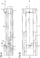
- FIG. 1 is a first embodiment of a semiconductor laser device according to the invention with reference to a sectional view in Figure 1A and a supervision in FIG. 1B shown schematically.
- a semiconductor laser chip 1 is arranged on a chip carrier comprising a heat sink 2, an electrical insulation layer 3 and a first terminal 4 and a second terminal 5.
- a pumped active region is monolithically integrated together with one or more pump radiation sources, such as edge-emitting lasers, which laterally optically pump the semiconductor laser chip 1.
- pump radiation sources such as edge-emitting lasers
- a bonding wire 11 is electrically conductively connected to the second terminal 5 and the semiconductor laser chip is fixed, for example via a solder connection, such as by means of a braze, on the first terminal 4 and electrically conductively connected thereto, wherein the solder joint both the attachment and the electrically conductive connection is used.
- the semiconductor laser chip 1 is preassembled on the chip carrier.
- the terminals 4, 5 contain, for example, copper and / or ensure sufficient heat dissipation of the heat generated at the semiconductor laser chip during operation through the insulating layer, which contains, for example, a ceramic, such as aluminum nitride, to the heat sink 2.
- Aluminum nitride is characterized by advantageously high thermal conductivity.
- the heat sink 2 contains, for example, copper.
- the chip carrier is thus preferably designed as a DBC substrate (DBC: Direct Bond Copper).
- the spacer elements 6 may, for example, as well as the carrier 7, contain or consist of a glass or silicon.
- the spacing elements are preferably on the chip carrier prior to placing the optical device on the chip carrier Carrier pre-assembled or formed by structuring the carrier.
- Carrier pre-assembled or formed by structuring the carrier.
- spacer elements made of glass, which are attached to the carrier by means of anodic bonding, gluing or soldering are suitable. Sawing with subsequent grinding and polishing of the corresponding surfaces of the spacer elements is particularly suitable for structuring the spacer elements out of the carrier.
- the radiation deflecting element and / or the external mirror is anodically bonded, glued or soldered to the carrier.
- the optical device is preferably mounted on the chip carrier via the spacer elements. For this purpose, for example, gluing or soldering is suitable.
- the radiation 13 generated in the semiconductor laser chip 1 by means of optical pumping of an active region of the semiconductor laser chip and emitted vertically to the surface 12 of the semiconductor laser chip is deflected via the radiation deflection element 8 to the external mirror 9 after passing through a recess 14 in the carrier 7.
- the recess may for example be etched or drilled in the carrier and is preferably as a gap or as in FIG. 1B shown in plan substantially circular.
- the radiation deflecting element 8 is embodied here as a glass prism which, for example, is provided by a reflector surface 80 with a highly reflective coating, for example a metallic or dielectric coating, for the radiation emitted by the semiconductor laser chip.
- the external mirror is limited in a preferred embodiment of the invention together with another mirror, which is preferably designed as integrated in the semiconductor laser chip Bragg mirror, the optical Resonator of the semiconductor laser device.
- the Bragg mirror preferably has a reflectivity of 99.9%.
- the external mirror is designed as a coupling-out mirror of laser radiation from the resonator and has, for example, a reflectivity of 96% or more.
- the mirror is designed concavely curved.
- the radius of curvature of the mirror is preferably 20 mm, particularly preferably 10 mm, or less, so that the beam radius of the radiation in the resonator can advantageously be kept low.
- Radiation generated in the semiconductor laser chip is amplified by means of induced emission in the active region of the semiconductor laser chip and partially coupled out via the external mirror 9.
- the beam radius in the resonator can be adapted to the size of the active area.
- it is optionally possible to force a basic mode operation of the semiconductor laser component for example by setting the beam cross-sectional area appropriately larger than the active area. Since radiation components outside of the active area are not amplified, higher modes can thus only increase correspondingly less.
- the radiation deflecting element 8 deflects the radiation incident on the radiation deflecting element from the semiconductor laser chip in a direction parallel to a main surface 15 of the carrier, preferably toward the external mirror 9.
- the carrier and the semiconductor laser chip are arranged relative to one another such that the radiation emitted vertically by the semiconductor laser chip is substantially perpendicular to the lateral one Main extension direction or main surface of the carrier is radiated and is deflected by the Strahlungsumlenkelement in a direction parallel to the main surface, preferably parallel to the main extension direction of the carrier.
- the surface 12 of the semiconductor laser chip and the carrier are preferably arranged substantially parallel to one another.
- the main surface 15 of the carrier 7 is substantially parallel to the surface 12 of the semiconductor laser chip 1 and / or the semiconductor laser chip 1 is pre-mounted on the chip carrier, that the surface 12 is substantially parallel to the chip carrier.
- the radiation deflecting element preferably deflects the incident radiation by an angle of 90 ° and is configured, for example, such that the reflector surface 80 encloses an angle of approximately 45 ° with the main surface 15 of the carrier.
- the folding of the resonator at the radiation deflecting element 8 facilitates the formation of a compact design of the semiconductor laser component and of the resonator.
- the optical device is preferably prefabricated and radiation deflecting element and external mirror are already correspondingly matched to a resonator, an adjustment of the external mirror for the optical resonator is required only with respect to the semiconductor laser chip.
- the optical device can be placed on a preassembled semiconductor laser chip as a resonator attachment and fixed on the chip carrier.
- An adjustment of the external mirror relative to the semiconductor laser chip can advantageously take place in the mounting plane of the optical device, preferably the plane of the chip carrier. On a complex three-dimensional adjustment of the mirror in the room can be dispensed with advantage.
- the semiconductor laser chip is formed in accordance with a semiconductor wafer laser or VECSEL.
- the wavelength of the radiation generated in the semiconductor laser chip is particularly preferably in the infrared spectral range, for example between 900 nm inclusive and 1100 nm inclusive, and may be approximately 920 nm, 1000 nm or 1040 nm.
- the semiconductor laser chip is based on this for preference to GaAs or AlGaAs.
- the semiconductor laser chip contains or is based on a III-V semiconductor material system, such as In x Gay Al 1-xy P, In x Gay Al 1-xy N or In x Ga y Al 1-xy As, each with 0 ⁇ x ⁇ 1, 0 ⁇ y ⁇ 1 and x + y ⁇ 1.
- a III-V semiconductor material system such as In x Gay Al 1-xy P, In x Gay Al 1-xy N or In x Ga y Al 1-xy As, each with 0 ⁇ x ⁇ 1, 0 ⁇ y ⁇ 1 and x + y ⁇ 1.
- materials made of the material system In x Ga y Al 1-xy As are particularly suitable.
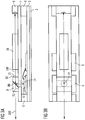
- FIG. 2 is a second embodiment of a semiconductor laser device according to the invention with reference to a sectional view in FIG. 2A and a supervision in FIG. 2B shown schematically.
- this embodiment corresponds to the in FIG. 1 shown embodiment.
- a non-linear optical element 16 is arranged for frequency conversion in the optical resonator and the decoupling is effected by the radiation deflecting element.
- Radiation 13 generated or amplified in the semiconductor laser chip strikes the radiation deflecting element 8, which is designed to be highly reflective for the radiation 13 via corresponding coating of the reflector surface 80, is deflected at the reflector surface 80 and passes through the non-linear optical element 16, in which a part of the radiation 13 is converted into frequency-converted radiation 160.
- the external mirror 9 which is preferably highly reflective for both radiations 13, 160 - for example with a reflectivity of 99.9% or more - and in contrast to FIG FIG. 1 is not designed for decoupling.
- the radiation 13 and the frequency-converted radiation 160 are reflected back in the direction of the radiation deflection element and again pass through the non-linear optical element, wherein a further portion of the radiation 13 is converted in frequency.
- the radiation 13 and the converted radiation 160 impinge on the radiation deflection element 8, which is highly reflective for the radiation 13 and highly transmissive for the frequency-converted radiation 160.
- the reflector surface 80 is preferably coated accordingly.
- the radiation 13 is thus fed to the semiconductor laser chip 1 for further amplification and the frequency-converted radiation 160 is coupled out of the resonator via the radiation deflecting element.
- the frequency-converted radiation is coupled out in such a way that it is radiated substantially parallel to the main extension direction of the carrier.
- the radiation deflecting element is designed as a prism. In the radiation decoupling, the radiation 160 is totally internally reflected internally on the surface 81 of the radiation deflection element facing away from the carrier and is coupled out of the resonator on the side of the radiation deflection element facing away from the nonlinear optical element.
- the radiation deflecting element is preferably polished accordingly smoothly for efficient total reflection by the surface 81.
- the non-linear optical element 16 is designed, for example, for frequency doubling (SHG) of the radiation amplified in the semiconductor laser chip.
- the non-linear optical element of infrared radiation produces green or blue radiation.
- Radiation of wavelength 920 nm can be converted into radiation of a wavelength of 460 nm.
- the nonlinear optical element is mounted on the carrier, for example by gluing or soldering.
- a nonlinear optical element suitable for frequency doubling, in particular for generating blue or green light may comprise, for example, a nonlinear crystal, such as a LBO (e.g., lithium triborate) or a BiBO (e.g., bismuth triborate) crystal.
- a nonlinear crystal such as a LBO (e.g., lithium triborate) or a BiBO (e.g., bismuth triborate) crystal.
- the nonlinear optical element may further comprise periodically poled (PP: Periodically Poled) quasi phase matched (QPM: quasi-phase matching) structures, such as PP-KTP (eg, KTiOPO 4 ), PP-LN (eg, PP-LiNbO 3 ), or PP -LT (eg PP-LiTaO 3 ) have.
- PP Periodically Poled
- QPM quasi-phase matching
- PP-KTP eg, KTiOPO 4
- PP-LN eg, PP-LiNbO 3
- PP -LT eg PP-LiTaO 3
- PP-QPM structures can also be used in MgO-doped or other stoichiometric material variants mentioned above.
- variants deviating from the abovementioned stoichiometric material variants for example of LiNbO 3 and LiTaO 3 , can also be used.
- QPM materials are characterized by high efficiency in frequency conversion even with a comparatively high radiation waist of the radiation in the nonlinear optical element.
- the efficiency is often heavily influenced by the beam waist and usually decreases with increasing beam waist.
- the radiation to be converted can be focused on the crystal via an optical element.
- focussing can be dispensed with in QPM materials because of the increased material-related efficiency.
- a plurality of PP-QPM structures can advantageously be produced simultaneously in a simplified manner in the laminated pane.
- such a non-linear optical element can advantageously be adapted to the specific properties of the semiconductor laser chip with advantage.
- the spectral and / or thermal acceptance width of the frequency conversion of such a nonlinear optical element can be adapted to the semiconductor laser chip or the radiation generated thereby.
- an aperiodically poled QPM structure can be used as a nonlinear optical element for frequency conversion.
- These structures are often distinguished from periodically poled structures by increased spectral acceptance, so that in light, such as temperature-induced fluctuations in the frequency of the radiation to be converted, the risk of reducing the efficiency of the frequency conversion in the nonlinear optical element is not significantly increased.
- the Strahlungsumlenkelement 8 designed as a beam splitter.
- the beam splitter is designed as a dichroic beam splitter.
- the beam splitter On the side of the surface 82, the beam splitter is preferably coated with an antireflection coating for the radiation 13 and the frequency-converted radiation 160, whereas on the reflector surface 80, which is formed on the coupling surface of the beam splitter, the radiation 13 reflects in the direction of the semiconductor laser chip and the frequency-converted radiation 160th is transmitted.
- This can be achieved, for example, by means of correspondingly highly reflective or highly transparent coatings on the part of the reflector surface 80 of the beam splitter.
- On the side facing the semiconductor laser chip surface or the surface 82 opposite surface of the beam splitter is preferably provided for the corresponding radiation with an anti-reflection coating.
- the radiation deflecting element in FIG. 3 radiates from the frequency-converted 160 and the non-frequency-converted radiation 13, wherein the radiation entrance sides are the same, the radiation exit sides, however, are different. Furthermore, the recess 14 is preferably completely covered by the radiation deflecting element 8.
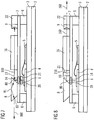
- FIG. 4 is a fourth embodiment of a semiconductor laser device according to the invention with reference to a sectional view in FIG. 4A and a supervision in FIG. 4B shown schematically.
- the radiation deflecting element 8, the non-linear optical element 16 and the external mirror 9 are arranged on the side of the carrier 7 facing the semiconductor laser chip.
- the radiation extraction from the resonator takes place via the radiation deflecting element 8.
- the radiation preferably exits the semiconductor laser component over the region of the beam-stabilizing elements 6 in which a window 17 for radiation decoupling is expediently provided.
- the spacer element 6 may for example contain or consist of silicon, a glass or a ceramic.
- the window 17 is preferably introduced into the spacer element 6 as a recess by means of drilling, etching or sawing.
- the window is preferably formed as a bore, etched hole, or cut-in gap in a spacer element or as a gap between two adjacent spacer elements.
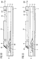
- FIG. 5 A fifth exemplary embodiment of a semiconductor laser component according to the invention is shown in FIG FIG. 5 by a sectional view in FIG. 5A and a supervision in FIG. 5B shown schematically and differs from that in FIG. 4 illustrated embodiment substantially in that the optical device is designed as a housing part for a housing of the semiconductor laser device.
- the carrier 7 is in this case as a housing cover and the spacer elements 6 are formed as a housing wall.
- the carrier preferably completely spans the semiconductor laser chip and still protrudes beyond the semiconductor laser chip.
- the spacing elements 6 preferably surround the semiconductor laser chip 1 on all sides, as in FIG FIG. 5B is shown. As a result, the protection of the semiconductor laser chip from harmful external influences is advantageously increased.
- the radiation deflecting element 8, the non-linear optical element 16 and the external mirror 9 on the side facing the semiconductor laser chip side of the carrier 7, approximately as in FIG. 5A , or on the semiconductor laser chip side facing away from the carrier, approximately corresponding to the FIG. 2 be arranged.
- the decoupling of radiation from the resonator is preferably carried out by a window 17, which may be formed in a spacing element or between two spacing elements.
- a recess may be provided in the carrier and radiation on the side facing away from the semiconductor laser chip side be coupled out of the resonator.
- any gaps present between two spacer elements that do not serve as windows, such as a gap 18, may be sealed with a sealant, such as an adhesive, for further protection against moisture or dust.
- the spacing elements 6 are structured out of the carrier, for example by sandblasting or etching.
- Carrier and spacer elements can thus be in one piece Structure be formed. The number of columns between spacer elements can thus be reduced.
- the spacer element is integrally formed and gap-free.
- a cavity for the semiconductor laser chip can be structured in the carrier.
- a substantially hermetic sealing of the housing for example against dust or moisture, can be facilitated.
- the housing of the semiconductor laser component comprises the chip carrier, the spacer elements 6 and the carrier 7, the carrier 7 forming the housing cover, the spacer elements the housing wall and the chip carrier the housing bottom of the semiconductor laser device.
- the lateral extent of the carrier is adapted for the formation as a housing cover preferably to that of the chip carrier. The formation of a comparatively planar surface of the semiconductor laser component is thus facilitated.
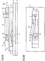
- FIG. 6 This in FIG. 6 by a sectional view in FIG. 6A and a supervision in FIG. 6B schematically illustrated sixth embodiment of a semiconductor laser device according to the invention substantially corresponds to the in FIG. 2 illustrated embodiment.
- a temperature control element 19 is provided for controlling the temperature of the nonlinear optical element.
- the tempering element 19 is preferably thermally conductively connected to the nonlinear optical element, arranged below the nonlinear optical element and / or directly adjacent to the nonlinear optical element.
- the tempering element 19 is integrated in the present embodiment as a heating resistor in the carrier 7. Zeckmenbine sample this contains the carrier a semiconductor material, such as silicon, and the Temper michselement is designed by means of suitable doping as a pn junction, which can be operated as a heating resistor. For a pn junction, for example, surface regions of the carrier are doped accordingly.
- an external, not in the carrier integrated Temper istselement which is preferably arranged between the carrier and the non-linear optical element may be provided.
- a metal thin film resistor, such as containing Pt, is particularly suitable for this purpose.
- temperature fluctuations of the nonlinear optical element can lead to fluctuations in the frequency of the frequency-converted radiation 160.
- the risk of such fluctuations can be reduced by controlling the temperature of the nonlinear optical element by means of the temperature control element 19.
- the tempering element 19 can be arranged both on the side of the carrier facing the non-linear optical element and on the side of the carrier facing away from the non-linear optical element. The latter is particularly advantageous if the nonlinear optical element, as in the FIGS. 4 or 5 , is arranged on the semiconductor laser chip side facing the carrier. An electrical control of the Temper michselements in operation of the semiconductor laser device can be facilitated.
- the distance, in particular the optical path, between the semiconductor laser chip and the radiation deflecting element, in particular to the reflector surface 80 is approximately 2 mm
- the distance from the radiation deflecting element to the surface of the nonlinear optical element facing the radiation deflecting element is 1.0 mm
- the distance between the external mirror facing surface of the nonlinear optical element and the external mirror about 0.5 mm.
- non-linear optical element for example, 4 mm for a crystal with critical phase matching, such as BiBo, or 3 mm for a PP-QPM structure, such as PP-LN.
- the end mirror in such a resonator with a radius of 20 mm has a spherically concave curvature, then approximately the following values result for the beam radius in the resonator: 53 ⁇ m on the semiconductor laser chip, 55 ⁇ m on the radiation deflecting element, 56 ⁇ m on the side of the nonlinear optical element facing the radiation deflecting element Elements, 62 microns at the surface of the non-linear optical element facing the external mirror and 63 microns at the external mirror.
- FIG. 7 A seventh exemplary embodiment of a semiconductor laser component according to the invention, which is shown schematically in a sectional view, essentially corresponds to that in FIG FIG. 2 shown.
- an optical element 20 for beam shaping and a wavelength filter 21 are arranged in the beam path in the resonator.
- the external mirror 9 is fixed to a support member 22.
- the optical element 20 is preferably arranged on the carrier 7 and fixed there.
- the optical element in the beam path in the resonator is arranged on the side of the carrier facing away from or facing away from the semiconductor laser chip.
- the optical element is arranged in the recess 14.
- the wavelength filter 21 is arranged on the semiconductor laser chip 1 side facing the carrier and preferably attached to the carrier.
- the optical element 20 is preferred designed to reduce the beam waist of the radiation to be converted 13. By focusing in the region of the nonlinear optical element, a particularly efficient frequency conversion can be achieved in the nonlinear optical element, in particular in a nonlinear, birefringent crystal.
- the efficiency of the frequency conversion can be further increased by the wavelength filter 21, the spectral width of the spectrum of the radiation to be converted, preferably infrared radiation, is reduced.
- the optical element can be designed, for example, as a lens, in particular with a focus, for example as a conventional focusing lens or as a GRIN (GRadienten INdex), Fresnel, or diffractive lens.
- a focus for example as a conventional focusing lens or as a GRIN (GRadienten INdex), Fresnel, or diffractive lens.
- GRIN GRadienten INdex
- Fresnel Fresnel
- diffractive lens diffractive lens
- a major plane of the lens or the wavelength filter may be parallel to or perpendicular to the main lateral extension direction of the carrier.
- the wavelength filter 21 for wavelength selection can be embodied for example as a dielectric filter, as a birefringent filter or as an etalon.
- a wavelength-selective effect can optionally also be achieved by a corresponding, preferably single-sided and / or dielectric, coating of the optical element 20.
- the external mirror 9 is not provided as a Resonatorendspiegel for coupling out of radiation and expediently highly reflective for the radiation 13 and the frequency-converted radiation 160 is formed.
- the radiation deflecting element 8 is designed to be highly transmissive for the frequency-converted radiation 160 and highly reflective for the radiation 13 on the part of the reflector surface 80.
- the optical element 20 and the wavelength filter 21 are preferably designed to be highly transmissive to the radiation 13. These reflection and transmission properties can be achieved by suitable coatings of the relevant surfaces of the external mirror, the radiation deflecting element, the optical element and / or the wavelength filter.
- the external mirror 9 may be designed, for example, substantially flat or concave. This is illustrated schematically by the dashed line in the external mirror 9, which indicates a concave external mirror.
- a planar design is facilitated by the beam shaping via the optical element 20, since the beam radius is advantageously kept low by the optical element and can be dispensed with beam shaping by the external mirror.
- FIG. 8 schematically illustrated eighth embodiment of a semiconductor laser device according to the invention substantially corresponds to in FIG. 7 illustrated embodiment.
- the wavelength filter 21 is arranged on the side of the carrier 7 facing away from the semiconductor laser chip 1.
- the radiation decoupling not by the Strahlungsumlenkelement 8, but by the external mirror. 9
- the external mirror is highly reflective for the radiation 13 and highly transmissive for the radiation 160.
- the reflector surface 80 of the radiation deflecting element 8 is designed to be reflective with respect to the radiation 13.
- a surface of the wavelength filter 21, preferably the surface 210 facing the non-linear optical element, is highly reflective with respect to the frequency-converted radiation 160 and highly transmissive to the radiation 13, so that the Proportion of the decoupled via the external mirror 9 frequency-converted radiation 160 is advantageously increased due to the reflection at the wavelength filter.
- the wavelength filter is expediently provided with a reflection coating for the radiation 160 or an antireflection coating for the radiation 13.
- FIG. 9 This in FIG. 9 by a sectional view in Figure 9A and a supervision in FIG. 9B schematically illustrated ninth embodiment of a semiconductor laser device according to the invention substantially corresponds to the in FIG. 8 shown embodiment.
- the optical element 20 for beam shaping is dispensed with.
- a further folding of the resonator is provided in this exemplary embodiment.
- This can also be a sufficiently small beam radius for efficient frequency conversion in the nonlinear optical element 16 can be achieved.
- the external mirror 9 is expediently concavely curved to reduce the beam waist and at the same time designed as Auskoppelapt and folding mirror.
- the resonator is limited by a further external mirror 23, which is preferably arranged on the carrier 7 and / or concavely curved.
- the non-linear optical element is arranged in the beam path between the mirrors 9 and 23.
- the mirror 23 is expediently designed to be highly reflective for the radiations 160 and 13. Due to the further folding of the resonator, the emission direction deviates from the direction of the radiation directed by the radiation deflecting element in the direction of the external mirror 9. Advantageously, the further folding can take place essentially in the plane parallel to the carrier 7. By such a convolution in the plane parallel to the carrier, the semiconductor laser device may optionally be compared with those described above Embodiments are made more compact and smaller.
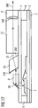
- FIG. 10 A tenth exemplary embodiment of a semiconductor laser component according to the invention, which is shown schematically on the basis of a sectional view, essentially corresponds to that in FIG. 1 shown.
- a non-linear optical element 16 is provided, and the radiation deflecting element is partially irradiated before the reflection at the reflector surface 80.
- the frequency-converted radiation 160 is coupled out of the resonator via the external mirror 9.
- a surface 84 of the radiation deflecting element a, in FIG. 10 dotted indicated, wavelength selective, preferably dielectric, coating, be applied.
- the reflection at the reflector surface 80 can be achieved by total internal reflection or by means of a suitable highly reflective coating. Such a coating is in FIG. 10 crossed indicated.
- FIG. 12 schematically illustrated by a sectional view twelfth embodiment of a semiconductor laser device according to the invention substantially corresponds to in FIG. 11 shown.
- a wavelength selection element 24 for wavelength selection such as a prism, arranged on the support.
- a wavelength selection can be achieved for example via a corresponding coating of a surface of the wavelength selection element 24 or by dispersion. Over the wavelength dependence of the refractive index 24 losses for certain modes in the resonator can be increased in the radiation passage through the wavelength selection element such that they are no longer amplified in the semiconductor laser chip.
- a wavelength-selective coating can, for example, light-entry side, as in FIG. 12 shown schematically at the surface 241, and / or at the light exit side by the surface 242, which is shown in FIG FIG. 12 is not shown, be provided.
- the light entry and light exit sides in this case relate to radiation impinging on the wavelength selection element from the radiation deflection element.
- FIG. 13 is a thirteenth embodiment of a semiconductor laser device according to the invention with reference to detail sectional views of a first variant in FIG. 13A and a second variant in FIG. 13B shown schematically.
- the wavelength selection element 24 in FIG. 13 arranged in the beam path of the semiconductor laser chip 1 ago on the Strahlungsumlenkelement 8 incident radiation.
- the radiation 13 strikes the wavelength selection element from the surface 240, is refracted there, traverses the wavelength selection element and is directed on the light exit side on the surface 241 in the direction of the radiation deflecting element.
- the wavelength-selection element can also be designed for polarization selection.
- the surface is expediently 240 formed such that the radiation 13 at least approximately below the Brewster angle on this surface.
- the reflection losses experienced by s-polarized light at the surface 240 are increased compared to p-polarized light.
- more p-polarized light is directed in the direction of the radiation deflecting element 8 (s-polarized denotes a linear polarization perpendicular to the plane of incidence and p-polarizes a linear polarization parallel to the plane of incidence).
- the wavelength selection element 24 is arranged on the part of the radiation deflecting element on the support 7, preferably between the radiation deflecting element and the support.
- the wavelength-selecting element 24 is fastened on the side of the carrier 7 opposite the radiation deflecting element and can completely cover the recess 14, for example.
- the wavelength selection element 24 can also be designed as a polarization selection element.
- the polarization state of the radiation in the resonator is schematically indicated by the arrows, with polarization emitted by the semiconductor laser chip rather than an unpolarized state and after the impingement of the radiation at the Brewster angle on or after passing through the wavelength selection element rather outweighs p-polarization.
- the radiation deflecting element has an uneven, preferably curved, surface which serves for beam shaping.
- this surface is spherical, aspherical, concave or convex curved and can, for example, by means of embossing, grinding, etching or molding be generated on Strahlungsumlenkelement.
- the surface is designed with different radii of curvature, in particular biradial, curved in order to prevent astigmatism of the radiation in the resonator.
- a biradial design has proved to be particularly advantageous in a spherical curvature. An astigmatism occurring at an angle of incidence of 45 ° can thus be avoided
- a curved surface for beam shaping and / or radiation deflection by reflection also be provided on an end face of the nonlinear optical element.
- the external mirror may be formed by a corresponding (partially) reflective coating of an end face of the nonlinear optical element.
- FIG. 14 is a fourteenth embodiment of a semiconductor laser device according to the invention schematically illustrated by a sectional view.
- FIG. 14 an optical device in a vertical arrangement with an external mirror 9, which is vertically spaced from the carrier 7, shown.
- the external mirror is spaced from the carrier by the radiation deflecting element 8, which is preferably designed as a beam splitter, and the non-linear optical element 16.
- Radiation 13 generated in the semiconductor laser chip 1 is radiated toward the external mirror 9 by the radiation deflecting element and the non-linear optical element, frequency-converted radiation 160 and radiation 13 are reflected at the external mirror and after re-passage
- the frequency-converted radiation is coupled out of the resonator by reflection, preferably by approximately 90 ° to the direction of incidence, at the reflector surface 80 and exit from the beam deflection element, preferably substantially parallel to the main extension direction of the carrier 7, by the nonlinear optical element.
- the radiation 13 is supplied to the semiconductor laser chip 1 for further amplification.
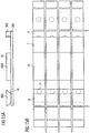
- FIG. 15 is an embodiment of a manufacturing method according to the invention with reference to a sectional view in Figure 15A and a supervision in FIG. 15B shown schematically.
- FIG. 15 shows a method for simultaneously producing a plurality of optical devices.
- a radiation deflecting strip 800 which is provided for forming a plurality of deflecting elements
- a mirror strip 900 which is provided for forming a plurality of external mirrors, are arranged on the carrier layer 700 on a carrier layer 700, such as a 6 "silicon wafer attached to anodic bonding.
- a plurality of recesses 14 provided for the later optical devices may be introduced into the carrier layer, possibly even before the radiation deflection strip 800 or the mirror strip 900 is mounted.
- radiation deflection strips 800 and mirror strips 900 can advantageously already be arranged on the carrier layer 700 and adjusted to one another in accordance with a later optical device.
- the radiation deflection strip and the mirror strip are adjusted to one another in accordance with the later optical device prior to attachment to the carrier layer.
- the recesses are preferably introduced before placing the elements on the carrier layer in this.
- a nonlinear optical element may also be disposed and fixed on the support layer as a strip 1600 provided to form a plurality of nonlinear optical elements, or as a single nonlinear optical element 16 in accordance with the later optical devices.
- the nonlinear optical element or the strip can be glued or soldered onto the carrier layer.
- a particularly efficient thermal coupling of the nonlinear optical element to a tempering element which is preferably integrated in the carrier layer, can be achieved.
- Spacing elements can be patterned out of the carrier layer by etching, for example as mesas from a silicon carrier layer, from the side facing away from the radiation deflecting strip and the mirror strip, or attached to the carrier layer as separate elements.
- a two-dimensional planar mirror structure for example by appropriate embossing in a substrate, for example from a glass, and any (partially) reflective coatings, may be prefabricated. From the mirror structure, a plurality of mirror strips can be obtained as a result.
- FIG. 15B Shown schematically on the basis of a plan view, after the attachment of the individual elements along the arrows into a plurality of optical devices each with a radiation deflecting element 8 and an external mirror 9 and optionally a nonlinear optical element 16 can be singulated.
- the separation can be done by sawing.
- a plurality of radiation deflecting or mirror strips can be arranged on the carrier layer.
- the method facilitates efficient production of a plurality of optical devices.
Landscapes
- Physics & Mathematics (AREA)
- Condensed Matter Physics & Semiconductors (AREA)
- General Physics & Mathematics (AREA)
- Electromagnetism (AREA)
- Optics & Photonics (AREA)
- Semiconductor Lasers (AREA)
- Lasers (AREA)
- Optical Modulation, Optical Deflection, Nonlinear Optics, Optical Demodulation, Optical Logic Elements (AREA)
Applications Claiming Priority (3)
| Application Number | Priority Date | Filing Date | Title |
|---|---|---|---|
| DE102004037019 | 2004-07-30 | ||
| DE102004050118A DE102004050118A1 (de) | 2004-07-30 | 2004-10-14 | Halbleiterlaserbauelement, optische Vorrichtung für ein Halbleiterlaserbauelement und Verfahren zur Herstellung einer optischen Vorrichtung |
| PCT/DE2005/001122 WO2006012819A1 (de) | 2004-07-30 | 2005-06-24 | Halbleiterlaserbauelement, optische vorrichtung für ein halbleiterlaserbauelement und verfahren zur herstellung einer optischen vorrichtung |
Publications (2)
| Publication Number | Publication Date |
|---|---|
| EP1771926A1 EP1771926A1 (de) | 2007-04-11 |
| EP1771926B1 true EP1771926B1 (de) | 2017-08-09 |
Family
ID=34972330
Family Applications (1)
| Application Number | Title | Priority Date | Filing Date |
|---|---|---|---|
| EP05759656.1A Ceased EP1771926B1 (de) | 2004-07-30 | 2005-06-24 | Halbleiterlaserbauelement, optische vorrichtung für ein halbleiterlaserbauelement und verfahren zur herstellung einer optischen vorrichtung |
Country Status (7)
| Country | Link |
|---|---|
| US (1) | US7860144B2 (enExample) |
| EP (1) | EP1771926B1 (enExample) |
| JP (1) | JP4886686B2 (enExample) |
| KR (1) | KR101156808B1 (enExample) |
| DE (1) | DE102004050118A1 (enExample) |
| TW (1) | TWI292246B (enExample) |
| WO (1) | WO2006012819A1 (enExample) |
Families Citing this family (24)
| Publication number | Priority date | Publication date | Assignee | Title |
|---|---|---|---|---|
| DE102006017293A1 (de) | 2005-12-30 | 2007-07-05 | Osram Opto Semiconductors Gmbh | Verfahren zur Herstellung einer optisch pumpbaren Halbleitervorrichtung |
| DE102006017294A1 (de) * | 2005-12-30 | 2007-07-05 | Osram Opto Semiconductors Gmbh | Optisch pumpbare Halbleitervorrichtung |
| AT503027B1 (de) * | 2006-05-08 | 2007-07-15 | Austria Tech & System Tech | Leiterplattenelement mit optoelektronischem bauelement und licht-wellenleiter |
| DE102006040263A1 (de) * | 2006-08-28 | 2008-03-06 | Osram Opto Semiconductors Gmbh | Optisches Element, optoelektronische Halbleitervorrichtung sowie Verfahren zur Herstellung eines optischen Elements |
| DE102006042195A1 (de) * | 2006-09-08 | 2008-03-27 | Osram Opto Semiconductors Gmbh | Etalon und optoelektronische Halbleitervorrichtung |
| DE102007004302A1 (de) * | 2006-09-29 | 2008-04-03 | Osram Opto Semiconductors Gmbh | Halbleiterchip und Verfahren zur Herstellung eines Halbleiterchips |
| JP2008198980A (ja) * | 2007-01-15 | 2008-08-28 | Seiko Epson Corp | レーザ光源装置、照明装置、画像表示装置、及びモニタ装置 |
| DE102007062047A1 (de) | 2007-12-21 | 2009-07-16 | Osram Opto Semiconductors Gmbh | Kompaktgehäuse |
| JP5024088B2 (ja) * | 2008-02-05 | 2012-09-12 | セイコーエプソン株式会社 | レーザ光源装置、照明装置、画像表示装置及びモニタ装置 |
| JP2009192873A (ja) * | 2008-02-15 | 2009-08-27 | Seiko Epson Corp | 光源装置、画像表示装置及びモニタ装置 |
| DE102008010297A1 (de) * | 2008-02-21 | 2009-10-29 | Osram Opto Semiconductors Gmbh | Frequenz-Konversions-Vorrichtung und Verfahren zur Herstellung einer Frequenz-Konversions-Vorrichtung |
| US7669366B2 (en) * | 2008-04-12 | 2010-03-02 | Felknor Ventures Llc | Plant retainer for retaining a plant for growth from the side or bottom of a planter |
| DE102008030818B4 (de) * | 2008-06-30 | 2022-03-03 | OSRAM Opto Semiconductors Gesellschaft mit beschränkter Haftung | Oberflächenemittierender Halbleiterlaser mit mehreren aktiven Zonen |
| DE102008052376A1 (de) * | 2008-10-20 | 2010-04-22 | Osram Opto Semiconductors Gmbh | Laseranordnung |
| KR101978013B1 (ko) * | 2012-01-20 | 2019-05-13 | 엑살로스 아게 | Oct를 위한 그리즘을 갖춘 파장-가변형 외부 캐비티 레이저 다이오드 |
| DE102012205513B4 (de) * | 2012-04-04 | 2021-12-09 | Osram Gmbh | Verfahren zum Herstellen einer Strahlungsanordnung und Strahlungsanordnung |
| US10043615B2 (en) * | 2012-10-08 | 2018-08-07 | Maxwell Technologies, Inc. | Electrode porosity for three-volt ultracapacitor |
| US10270224B2 (en) * | 2015-06-04 | 2019-04-23 | Nlight, Inc. | Angled DBR-grating laser/amplifier with one or more mode-hopping regions |
| EP3130950A1 (de) | 2015-08-10 | 2017-02-15 | Multiphoton Optics Gmbh | Strahlumlenkelement sowie optisches bauelement mit strahlumlenkelement |
| DE102016107499A1 (de) * | 2016-04-22 | 2017-10-26 | Fraunhofer-Gesellschaft zur Förderung der angewandten Forschung e.V. | Frequenzverdoppler sowie Verfahren zum Erzeugen elektromagnetischer Strahlung |
| DE102016107715A1 (de) * | 2016-04-26 | 2017-10-26 | Osram Opto Semiconductors Gmbh | Lasermodul mit einem optischen Bauteil |
| US10263391B2 (en) * | 2017-09-07 | 2019-04-16 | Apple Inc. | Horizontal external-cavity laser geometry |
| EP4033621B1 (en) | 2019-09-20 | 2023-11-01 | Nichia Corporation | Light source device and method of manufacturing the same |
| DE102019215098A1 (de) * | 2019-10-01 | 2021-04-01 | Robert Bosch Gmbh | Mikromechanisch-optisches Bauteil und Herstellungsverfahren |
Family Cites Families (15)
| Publication number | Priority date | Publication date | Assignee | Title |
|---|---|---|---|---|
| AU659270B2 (en) * | 1992-02-20 | 1995-05-11 | Sony Corporation | Laser light beam generating apparatus |
| DE19536880B4 (de) * | 1995-09-01 | 2006-08-24 | Fraunhofer-Gesellschaft zur Förderung der angewandten Forschung e.V. | Laseranordnung zur Skalierung von frequenzverdoppelten Lasern |
| WO1997009759A1 (de) | 1995-09-01 | 1997-03-13 | Fraunhofer-Gesellschaft zur Förderung der angewandten Forschung e.V. | Laseranordnung und verfahren zur skalierung von frequenzverdoppelten lasern |
| DE19548647C2 (de) | 1995-12-14 | 2003-01-23 | Manfred Gabbert | Durchstimmbare, justierstabile Halbleiterlaserlichtquelle sowie ein Verfahren zur optisch stabilen, weitgehend kontinuierlichen Durchstimmung von Halbleiterlasern |
| US6002695A (en) * | 1996-05-31 | 1999-12-14 | Dpss Lasers, Inc. | High efficiency high repetition rate, intra-cavity tripled diode pumped solid state laser |
| GB2325334B (en) | 1998-07-10 | 1999-04-14 | Bookham Technology Ltd | External cavity laser |
| DE19929878A1 (de) | 1999-06-29 | 2001-01-04 | Bosch Gmbh Robert | Träger zur Montage optoelektronischer Bauteile und Verfahren zur Herstellung |
| EP1513006B1 (en) | 1999-10-28 | 2010-12-15 | FUJIFILM Corporation | Light wavelength converting system |
| JP2001230492A (ja) * | 2000-02-21 | 2001-08-24 | Fuji Photo Film Co Ltd | 半導体発光装置 |
| US6711203B1 (en) * | 2000-09-22 | 2004-03-23 | Blueleaf, Inc. | Optical transmitter comprising a stepwise tunable laser |
| US6862301B2 (en) * | 2001-12-31 | 2005-03-01 | Finisar Corporation | Tunable laser assembly |
| DE10214120B4 (de) * | 2002-03-28 | 2007-06-06 | Osram Opto Semiconductors Gmbh | Optisch pumpbare oberflächenemittierende Halbleiterlaservorrichtung |
| DE10241192A1 (de) * | 2002-09-05 | 2004-03-11 | Osram Opto Semiconductors Gmbh | Optisch gepumpte strahlungsemittierende Halbleitervorrichtung und Verfahren zu deren Herstellung |
| DE10253907A1 (de) | 2002-09-20 | 2004-04-01 | Osram Opto Semiconductors Gmbh | Optischer Abtastkopf und Verfahren zur Herstellung desselben |
| JP2004221321A (ja) * | 2003-01-15 | 2004-08-05 | Mitsubishi Electric Corp | 波長可変半導体光装置 |
-
2004
- 2004-10-14 DE DE102004050118A patent/DE102004050118A1/de not_active Withdrawn
-
2005
- 2005-06-24 JP JP2007522906A patent/JP4886686B2/ja not_active Expired - Fee Related
- 2005-06-24 KR KR1020077004813A patent/KR101156808B1/ko not_active Expired - Fee Related
- 2005-06-24 WO PCT/DE2005/001122 patent/WO2006012819A1/de not_active Ceased
- 2005-06-24 US US11/659,065 patent/US7860144B2/en not_active Expired - Fee Related
- 2005-06-24 EP EP05759656.1A patent/EP1771926B1/de not_active Ceased
- 2005-07-27 TW TW094125358A patent/TWI292246B/zh not_active IP Right Cessation
Non-Patent Citations (1)
| Title |
|---|
| None * |
Also Published As
| Publication number | Publication date |
|---|---|
| US7860144B2 (en) | 2010-12-28 |
| DE102004050118A1 (de) | 2006-03-23 |
| US20090225797A1 (en) | 2009-09-10 |
| WO2006012819A1 (de) | 2006-02-09 |
| TW200610241A (en) | 2006-03-16 |
| JP4886686B2 (ja) | 2012-02-29 |
| TWI292246B (en) | 2008-01-01 |
| EP1771926A1 (de) | 2007-04-11 |
| KR20070047332A (ko) | 2007-05-04 |
| JP2008508698A (ja) | 2008-03-21 |
| KR101156808B1 (ko) | 2012-06-18 |
Similar Documents
| Publication | Publication Date | Title |
|---|---|---|
| WO2006012819A1 (de) | Halbleiterlaserbauelement, optische vorrichtung für ein halbleiterlaserbauelement und verfahren zur herstellung einer optischen vorrichtung | |
| DE69112217T2 (de) | Lasermatrix in form eines mikrochips. | |
| DE60033839T2 (de) | Abstimmbare ADD/DROP UND CROSS-CONNECT Vorrichtungen | |
| JP2008508698A5 (enExample) | ||
| DE112005003025T5 (de) | Modifikationen eines nicht-linearen Kristalls für eine haltbare Hochleistungs-Laserwellenlängen-Umwandlung | |
| DE112015000391T5 (de) | Lichtemittierende Vorrichtung mit externem Resonator | |
| EP1966858B1 (de) | Vertikal emittierender, optisch gepumpter halbleiter mit externem resonator und frequenzverdopplung auf separatem substrat | |
| DE112015002094B4 (de) | Lichtemittierende Vorrichtung des äußeren Resonatortyps | |
| EP1708319B1 (de) | Laservorrichtung | |
| DE60014074T2 (de) | Diodenlasergepumpter festkörperlaser | |
| EP1966857B1 (de) | Vertikal emittierender, optisch gepumpter halbleiter mit externem resonator auf separatem substrat | |
| DE102008048903B4 (de) | Optoelektronisches Bauteil | |
| DE102004012014B4 (de) | Scheibenlaser mit einer Pumpanordnung | |
| DE102021113856A1 (de) | Optoelektronischer halbleiterchip und bauteil | |
| EP2308142B1 (de) | Halbleiterlaser mit einem optisch nichtlinearen kristall | |
| DE19523267A1 (de) | Lasermodul | |
| WO2008028454A1 (de) | Etalon und optoelektronische halbleitervorrichtung | |
| EP1770834B1 (de) | Optisch gepumpter oberflächenemittierender Halbleiterlaser und optische Projektionsvorrichtung mit solch einem Halbleiterlaser | |
| JP5311710B2 (ja) | 半導体構成素子及び半導体構成素子の製造方法 | |
| EP2091117A2 (de) | Halbleiterlasermodul | |
| JP2006060239A5 (enExample) | ||
| DE102004040080B4 (de) | Optisch gepumpte Halbleiter-Laservorrichtung | |
| WO2010045916A1 (de) | Vcsel mit temperatur-eingestelltem lyot-filter bestehend aus einem polarisator und einem frequenz-verdoppelnden kristall | |
| DE102006040263A1 (de) | Optisches Element, optoelektronische Halbleitervorrichtung sowie Verfahren zur Herstellung eines optischen Elements |
Legal Events
| Date | Code | Title | Description |
|---|---|---|---|
| PUAI | Public reference made under article 153(3) epc to a published international application that has entered the european phase |
Free format text: ORIGINAL CODE: 0009012 |
|
| 17P | Request for examination filed |
Effective date: 20061227 |
|
| AK | Designated contracting states |
Kind code of ref document: A1 Designated state(s): DE |
|
| RIN1 | Information on inventor provided before grant (corrected) |
Inventor name: SINGER, FRANK Inventor name: STEEGMUELLER, ULRICH Inventor name: SCHWARZ, THOMAS Inventor name: KUEHNELT, MICHAEL |
|
| DAX | Request for extension of the european patent (deleted) | ||
| RBV | Designated contracting states (corrected) |
Designated state(s): DE |
|
| 17Q | First examination report despatched |
Effective date: 20080121 |
|
| RAP1 | Party data changed (applicant data changed or rights of an application transferred) |
Owner name: OSRAM OPTO SEMICONDUCTORS GMBH |
|
| RAP1 | Party data changed (applicant data changed or rights of an application transferred) |
Owner name: OSRAM OPTO SEMICONDUCTORS GMBH |
|
| GRAP | Despatch of communication of intention to grant a patent |
Free format text: ORIGINAL CODE: EPIDOSNIGR1 |
|
| RIC1 | Information provided on ipc code assigned before grant |
Ipc: H01S 3/109 20060101ALN20170330BHEP Ipc: H01S 3/081 20060101ALN20170330BHEP Ipc: H01S 5/04 20060101ALN20170330BHEP Ipc: H01S 5/022 20060101ALI20170330BHEP Ipc: H01S 5/183 20060101ALI20170330BHEP Ipc: H01S 5/14 20060101AFI20170330BHEP |
|
| RIC1 | Information provided on ipc code assigned before grant |
Ipc: H01S 3/109 20060101ALN20170331BHEP Ipc: H01S 5/183 20060101ALI20170331BHEP Ipc: H01S 5/14 20060101AFI20170331BHEP Ipc: H01S 5/04 20060101ALN20170331BHEP Ipc: H01S 3/081 20060101ALN20170331BHEP Ipc: H01S 5/022 20060101ALI20170331BHEP |
|
| INTG | Intention to grant announced |
Effective date: 20170421 |
|
| GRAS | Grant fee paid |
Free format text: ORIGINAL CODE: EPIDOSNIGR3 |
|
| GRAA | (expected) grant |
Free format text: ORIGINAL CODE: 0009210 |
|
| AK | Designated contracting states |
Kind code of ref document: B1 Designated state(s): DE |
|
| RIN1 | Information on inventor provided before grant (corrected) |
Inventor name: KUEHNELT, MICHAEL Inventor name: STEEGMUELLER, ULRICH Inventor name: SINGER, FRANK Inventor name: SCHWARZ, THOMAS |
|
| REG | Reference to a national code |
Ref country code: DE Ref legal event code: R096 Ref document number: 502005015664 Country of ref document: DE |
|
| REG | Reference to a national code |
Ref country code: DE Ref legal event code: R097 Ref document number: 502005015664 Country of ref document: DE |
|
| PLBE | No opposition filed within time limit |
Free format text: ORIGINAL CODE: 0009261 |
|
| STAA | Information on the status of an ep patent application or granted ep patent |
Free format text: STATUS: NO OPPOSITION FILED WITHIN TIME LIMIT |
|
| 26N | No opposition filed |
Effective date: 20180511 |
|
| PGFP | Annual fee paid to national office [announced via postgrant information from national office to epo] |
Ref country code: DE Payment date: 20210618 Year of fee payment: 17 |
|
| REG | Reference to a national code |
Ref country code: DE Ref legal event code: R119 Ref document number: 502005015664 Country of ref document: DE |
|
| PG25 | Lapsed in a contracting state [announced via postgrant information from national office to epo] |
Ref country code: DE Free format text: LAPSE BECAUSE OF NON-PAYMENT OF DUE FEES Effective date: 20230103 |