EP1770659B1 - Portable electronic device and IC card - Google Patents
Portable electronic device and IC card Download PDFInfo
- Publication number
- EP1770659B1 EP1770659B1 EP06018460.3A EP06018460A EP1770659B1 EP 1770659 B1 EP1770659 B1 EP 1770659B1 EP 06018460 A EP06018460 A EP 06018460A EP 1770659 B1 EP1770659 B1 EP 1770659B1
- Authority
- EP
- European Patent Office
- Prior art keywords
- data
- child
- value
- card
- read
- Prior art date
- Legal status (The legal status is an assumption and is not a legal conclusion. Google has not performed a legal analysis and makes no representation as to the accuracy of the status listed.)
- Active
Links
Images


Classifications
-
- G—PHYSICS
- G06—COMPUTING OR CALCULATING; COUNTING
- G06K—GRAPHICAL DATA READING; PRESENTATION OF DATA; RECORD CARRIERS; HANDLING RECORD CARRIERS
- G06K17/00—Methods or arrangements for effecting co-operative working between equipments covered by two or more of main groups G06K1/00 - G06K15/00, e.g. automatic card files incorporating conveying and reading operations
-
- G—PHYSICS
- G07—CHECKING-DEVICES
- G07F—COIN-FREED OR LIKE APPARATUS
- G07F7/00—Mechanisms actuated by objects other than coins to free or to actuate vending, hiring, coin or paper currency dispensing or refunding apparatus
- G07F7/08—Mechanisms actuated by objects other than coins to free or to actuate vending, hiring, coin or paper currency dispensing or refunding apparatus by coded identity card or credit card or other personal identification means
- G07F7/10—Mechanisms actuated by objects other than coins to free or to actuate vending, hiring, coin or paper currency dispensing or refunding apparatus by coded identity card or credit card or other personal identification means together with a coded signal, e.g. in the form of personal identification information, like personal identification number [PIN] or biometric data
- G07F7/1008—Active credit-cards provided with means to personalise their use, e.g. with PIN-introduction/comparison system
-
- G—PHYSICS
- G06—COMPUTING OR CALCULATING; COUNTING
- G06K—GRAPHICAL DATA READING; PRESENTATION OF DATA; RECORD CARRIERS; HANDLING RECORD CARRIERS
- G06K19/00—Record carriers for use with machines and with at least a part designed to carry digital markings
- G06K19/06—Record carriers for use with machines and with at least a part designed to carry digital markings characterised by the kind of the digital marking, e.g. shape, nature, code
- G06K19/067—Record carriers with conductive marks, printed circuits or semiconductor circuit elements, e.g. credit or identity cards also with resonating or responding marks without active components
- G06K19/07—Record carriers with conductive marks, printed circuits or semiconductor circuit elements, e.g. credit or identity cards also with resonating or responding marks without active components with integrated circuit chips
-
- G—PHYSICS
- G06—COMPUTING OR CALCULATING; COUNTING
- G06Q—INFORMATION AND COMMUNICATION TECHNOLOGY [ICT] SPECIALLY ADAPTED FOR ADMINISTRATIVE, COMMERCIAL, FINANCIAL, MANAGERIAL OR SUPERVISORY PURPOSES; SYSTEMS OR METHODS SPECIALLY ADAPTED FOR ADMINISTRATIVE, COMMERCIAL, FINANCIAL, MANAGERIAL OR SUPERVISORY PURPOSES, NOT OTHERWISE PROVIDED FOR
- G06Q20/00—Payment architectures, schemes or protocols
- G06Q20/30—Payment architectures, schemes or protocols characterised by the use of specific devices or networks
- G06Q20/34—Payment architectures, schemes or protocols characterised by the use of specific devices or networks using cards, e.g. integrated circuit [IC] cards or magnetic cards
- G06Q20/341—Active cards, i.e. cards including their own processing means, e.g. including an IC or chip
-
- G—PHYSICS
- G06—COMPUTING OR CALCULATING; COUNTING
- G06Q—INFORMATION AND COMMUNICATION TECHNOLOGY [ICT] SPECIALLY ADAPTED FOR ADMINISTRATIVE, COMMERCIAL, FINANCIAL, MANAGERIAL OR SUPERVISORY PURPOSES; SYSTEMS OR METHODS SPECIALLY ADAPTED FOR ADMINISTRATIVE, COMMERCIAL, FINANCIAL, MANAGERIAL OR SUPERVISORY PURPOSES, NOT OTHERWISE PROVIDED FOR
- G06Q20/00—Payment architectures, schemes or protocols
- G06Q20/30—Payment architectures, schemes or protocols characterised by the use of specific devices or networks
- G06Q20/34—Payment architectures, schemes or protocols characterised by the use of specific devices or networks using cards, e.g. integrated circuit [IC] cards or magnetic cards
- G06Q20/357—Cards having a plurality of specified features
- G06Q20/3576—Multiple memory zones on card
- G06Q20/35765—Access rights to memory zones
Definitions
- the present invention relates to a portable electronic device and an IC card which have, for example, a writable/rewritable nonvolatile memory and a control element such as a central processing unit (CPU) and which execute various kinds of processing on the basis of instruction data supplied from the external.
- a portable electronic device and an IC card which have, for example, a writable/rewritable nonvolatile memory and a control element such as a central processing unit (CPU) and which execute various kinds of processing on the basis of instruction data supplied from the external.
- CPU central processing unit
- a portable electronic device there has been an IC card in which an IC module having functions of a memory, a CPU, etc, is embedded in a case constructed by plastic plates and others.
- data is written into a rewritable nonvolatile memory in response to a command from an external device, or data is read from the nonvolatile memory.
- data comprising an identifier, length information and a data portion is defined.
- the identifier indicates the kind of data.
- the length information indicates the length of the data.
- the data portion stores the data itself.
- Some of the data used for the IC card have a so-called nested structure.
- the data having the nested structure is identified by, for example, the identifier.
- a structured tag field is defined with regard to data having the nested structure by, for example, Annex D to ISO/IEC 7816.
- EP 1 085 395 A2 discloses an access control system for files on a memory card, the memory card including a plurality of data files and a control file, which comprises control information for determining whether data read from a data file is authorized to include the data type of the data read therefrom.
- JP 05002536 A discloses an IC card for correcting or erasing data and preventing the reading of incorrect data or unnecessary data.
- FIG. 1 shows an example of the configuration of an IC card system including an IC card as a portable electronic device according to the present invention.
- This IC card system comprises an IC card 11, a card reader/writer 12, a terminal device 13, a keyboard 14, a display device (CRT) 15, a printer 16, etc.
- CTR display device
- the IC card 11 is capable of communicating with the terminal device 13 via the card reader/writer 12.
- the card reader/writer 12 has a communication unit using a communication method complying with the IC card 11.
- the terminal device 13 comprises, for example, a personal computer having a control unit, a memory, various interfaces, etc.
- the control unit executes a control program stored in the memory to achieve various functions.
- the keyboard 14 functions as an operation unit.
- the keyboard 14 supplies to the terminal device 13 signals indicating keys with which input has been performed.
- the display device 15 performs various kinds of display in accordance with display control by the terminal device 13.
- the display device 15 comprises a CRT or a liquid crystal display.
- the printer 16 prints print data supplied from the terminal device 13.
- FIG. 2 is a diagram for explaining the example of the configuration of the IC card 11.
- the IC card 11 contains a module 11b in a case forming a main body 11a. Further, a magnetic stripe portion 101 is provided on the surface of the main body 11a of the IC card 11.
- the magnetic stripe portion 101 is provided on the surface of the card main body 11a.
- the magnetic stripe portion 101 comprises a magnetic storage unit.
- the module 11b has a communication unit 102, a CPU 104, a data memory 105, a working memory 106, a program memory 107, etc.
- the module 11b comprises an IC chip and an interface portion that are integrally IC-modularized in a connected state.
- the module 11b is buried in the main body 11a of the IC card.
- the communication unit 102 performs data communication with the reader/writer 12.
- the communication unit 102 comprises a communication control section and an interface section.
- the communication unit 102 has a configuration complying with the communication method of the IC card 11.
- the communication unit 102 enables a communication method of a contactless-type (wireless) IC card or a contact-type IC card.
- the communication unit 102 comprises an antenna as the interface section and the communication control section.
- the communication unit 102 receives by the antenna modulated waves transmitted from the reader/writer 12, and demodulates the received modulated waves by the communication control section.
- the communication unit 102 causes the communication control section to modulate data to be sent to the external, and sends the modulated signal as modulated waves by the antenna. Further, the communication unit 102 generates, from the modulated waves received by the antenna, a power source and a clock to be supplied to internal circuits.
- the communication unit 102 comprises a contact section.
- the contact section contacts an IC card terminal portion (not shown) provided in the reader/writer 12.
- the contact section transmits/receives data to/from the reader/writer. Further, the power source and the clock obtained from the reader/writer 12 via the contact section are supplied to each unit in the IC card 11.
- the communication control unit of the communication unit 102, the CPU 104, the data memory 105, the working memory 106 and the program memory 107 are constituted by one or a plurality of IC chips 103.
- the IC chip 103 is connected with the interface of the communication unit 102 to integrally constitute the module 11b.
- the CPU 104 is a control unit for achieving various kinds of processing on the basis of the control program and control data stored in the program memory 107 or the data memory 105.
- the CPU 104 performs various kinds of determination processing, judgment processing, data processing (data writing, data reading), etc.
- the data memory 105 comprises a nonvolatile memory such as an electronically erasable and programmable read only memory (EEPROM) capable of erasing or rewriting data.
- the data memory 105 stores, for example, data for applications as functions to be achieved by the IC card 11. It is to be noted that the data memory 105 stores, for example, as functions to be achieved by the IC card 11, data for applications to enable functions such as a credit card function, a card function for a customer loyalty system and an ID card function.
- EEPROM electronically erasable and programmable read only memory
- the working memory 106 comprises a volatile memory such as a random access memory (RAM).
- the working memory 106 functions, for example, as a memory for an operation of temporarily retaining processing data.
- the working memory 106 temporarily stores, for example, processing data being executed by the CPU 104, transmission data to be transmitted by the communication unit 102 or data received by the communication unit 102.
- the working memory 106 is provided with an output counter 106a, a read pointer 106b, an output buffer 106c, a read range counter 106d, etc.
- the output counter 106a, the read pointer 106b, the output buffer 106c and the read range counter 106d will be described later in detail.
- the program memory 107 comprises unrewritable fixed memory such as a mask read only memory (ROM).
- the program memory 107 stores, for example, a control program of the CPU 104.
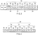
- FIG. 3 shows an example of the configuration of data stored in the data memory 105.
- the data shown in FIG. 3 is data having a nested structure. It is to be noted that the data shown in FIG. 3 is stored in the data memory 105 as an elementary file (EF) here.
- EF elementary file
- the data comprises an identifier (TAG) 201 indicating the kind of the entire data, length information (LEN) 202 indicating the length of the data (a data portion 203), and the data portion (value) 203 for storing the data itself.
- TAG identifier
- LN length information
- value value
- the identifier 201 is also called a parent identifier
- the length information 202 is also called parent length information
- the data portion 203 is also called a parent data portion, and that the entire data comprising the identifier 201, the length information 202 and the data portion 203 is also called parent data.
- the parent identifier (TAG) 201 indicates the kind of the parent data.
- the parent length information 202 indicates the length of the parent data portion 203.
- the parent data portion 203 stores the parent data itself (here, a plurality of child data described later).
- a particular value e.g., "00" indicating that the parent data is invalid is set in the parent identifier 201.
- the parent data portion 203 further stores a plurality of data 207, 211, 215 and 219.
- the data 207, 211, 215 and 219 comprise identifiers (T1, T2, T3 and T4) 204, 208, 212 and 216, length information (L1, L2, L3 and L4) 205, 209, 213 and 217, and data portions (V1, V2, V3 and V4) 206, 210, 214 and 218, respectively.
- the data 207, 211, 215 and 219 are also referred to as child data (first, second, third and fourth child data) here.
- the identifiers (T1, T2, T3 and T4) 204, 208, 212 and 216 are also referred to as child identifiers (first, second, third and fourth child identifiers).
- the length information (L1, L2, L3 and L4) 205, 209, 213 and 217 are also referred to as child length information (first, second, third and fourth child length information).
- the data portions (V1, V2, V3 and V4) 206, 210, 214 and 218 are also referred to as child data portions (first, second, third and fourth child data portions).
- the parent data portion 203 of the parent data shown in FIG. 3 stores the first child data 207 comprising the first child identifier (T1) 204, the first child length information (L1) 205 and the first child data portion (V1) 206, the second child data 211 comprising the second child identifier (T2) 208, the second child length information (L2) 209 and the second child data portion (V2) 210, the third child data 215 comprising the third child identifier (T3) 212, the third child length information (L3) 213 and the third child data portion (V3) 214, and the fourth child data 219 comprising the fourth child identifier (T4) 216, the fourth child length information (L4) 217 and the fourth child data portion (V4) 218.
- first, second, third and fourth child data 207, 211, 215 and 219 are stored in the parent data portion 203 in a combined state.
- a particular value e.g., "00" indicating that this child data is invalid is set in the child identifier 204 (or 208, 212, 216) of the child data.
- a data structure as described above is also referred to as a TLV structure.
- FIG. 4 is a diagram showing a specific example of the data having the nested structure.
- each of the parent identifier 201, the first child identifier 204, the second child identifier 208, the third child identifier 212, the parent length information 202, the first child length information 205, the second child length information 209 and the third child length information 213 is 1-byte (8-bit) data.
- the parent data portion 203 and the first child data portion 206 are 1-byte (8-bit) data
- the second child data portion 210 (210a, 210b) are 2-byte (16-bit) data
- the third child data portion 214 (214a, 214b, 214c) are 3-byte (24-bit) data.
- FIGS. 5 and 6 are flowcharts for explaining the processing of reading the nested structure data in response to a data read command.
- FIGS. 7, 8 , 9 and 10 are diagrams for explaining the relation among the value of the output counter 106a, the value of the read pointer 106b and data stored in the output buffer in the reading processing intended to read the data having the nested structure shown in FIG. 4 .
- FIGS. 4 , 7 , 8 , 9 and 10 the processing of reading the nested structure data will be described properly referring to FIGS. 4 , 7 , 8 , 9 and 10 in addition to the flowcharts shown in FIGS. 5 and 6 .
- the card reader/writer 12 as an external device has transmitted a data read command to the IC card 11.
- the above data read command is a data read command which has specified the data having the nested structure by the identifier (a command to require the read of the nested structure data).
- the data read command transmitted from the card reader/writer 12 is received by the communication unit 102 of the IC card 11 (step S1).
- the data read command received by the communication unit 102 is supplied from the communication unit 102 to the CPU 104.
- the CPU 104 of the IC card 11 judges whether or not data to be read (parent data) specified by the command exists in the data memory 105 (step S2).
- the CPU 104 When this judgment is that the data to be read specified by the command does not exist, the CPU 104 returns a response implying an error to the card reader/writer 12, and terminates the processing.
- the CPU 104 copies first one byte of the data (parent data) to a first one byte of the output buffer 106c provided in the working memory 106 (step S3).
- the first one byte is the parent identifier 201 in the data having the configuration shown in FIG. 4 . Therefore, data "97" stored in the parent identifier 201 is copied into the head (first byte) of the output counter 106a in the working memory 106.
- the CPU 104 sets a numerical value "2" in the output counter 106a provided in the working memory 106, and sets in the read pointer 106b "2" indicating the head position of the data portion 203 of the parent data, and further sets the value of the parent length information 202 in the read range counter 106d (step S4).
- the output counter 106a indicates the number of bytes written into the output buffer 106c.
- the second byte in the output buffer 106c is free.
- the second byte in the output buffer 106c is intended to store data indicating the length of the entire data finally output in the processing described later.
- data indicating the reading position in the data is stored in the read pointer 106b.
- the read pointer 106b indicates the first child identifier 204 storing "11".
- the read range counter 106d stores a value indicating the length of remaining data to be read.
- the value of the parent length information in the parent data is set in the read range counter 106d.
- the read range counter 106d shows "0" this means that there is no remaining data to be read.
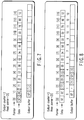
- FIG. 7 shows the value of the output counter 106a, the value of the read pointer and data stored in the output buffer 106c in a situation where the processing up to step S4 has been completed in the data reading processing shown in FIG. 4 .
- " 2 " is stored in the output counter 106a
- "2" is stored in the read pointer 106b
- one byte of data read from the head of the data i.e., the parent identifier "97" of the specified parent data
- the CPU 104 subtracts "the value of the child length information for the child data + 2" from the value of the read range counter 106d (step S7). For example, when the identifier of the first child data is read, the CPU 104 sets the value of [the length information for the parent data - (the child length information + 2)] in the read range counter 106d.
- the CPU 104 judges whether or not it shows a particular value (e.g., "00") indicating that the child identifier (e.g., the first child identifier 204) read in step S5 is invalid (step S8).
- a particular value e.g., "00"
- the CPU 104 reads the child length information as the data on the position indicated by the value of the read pointer 106b, and temporarily stores the read child length information in the working memory 106 (step S9). For example, in the data shown in FIG. 4 , when the value of the read pointer 106b is "3", the CPU 104 reads the child length information 205 whose data value is "01”, and temporarily stores the information in the working memory 106.
- the CPU 104 copies data on the child identifier and data on the child length information temporarily stored in the working memory 106 (e.g., "11" as the data on the first child identifier 204 and "01" as the first child length information 205) into the output buffer 106c (step S10). At this point, the CPU 104 decides the position for writing data in the output buffer 106c on the basis of the position indicated by the value of the output counter 106a.
- the CPU 104 copies the data on the child identifier (e.g., the data on the first child identifier) into the third byte in the output buffer 106c, and copies the data on the child identifier (e.g., the data on the first child length information) into the fourth byte.
- the CPU 104 puts "+2" on the value of the output counter 106a in the working memory 106, and adds one to the value of the read pointer 106b (step S11).
- the CPU 104 When the values of the output counter 106a and the read pointer 106b are updated in step S11 the CPU 104 reads the data in the first one byte (i.e., the first one byte in the child data portion) from the position indicated by the value of the read pointer 106b (step S12), and copies the read data into the output buffer 106c in the working memory 106 (step S13). At this point, the CPU 104 copies the read one byte of data into the output buffer 106c. It is to be noted that the CPU 104 may judge the position in the output buffer 106c for storing the read one byte of data on the basis of the value of the output counter 106a.
- the CPU 104 When the one byte of data read from the child data portion has been copied into the output buffer 106c, the child data portion, the CPU 104 performs the processing of putting "+1" on the value of the output counter 106a, putting "+1” on the read pointer 106b and subtracting "the number of bytes read from the child data portion" from "the value of the child length information" (step S14). For example, when the data of the first one byte is read from the child data portion, the CPU 104 calculates the value "(the value of the child length information) - 1". Moreover, when the two bytes of data are read from the child data portion, the CPU 104 calculates the value "(the value of the child length information) - 2".
- step S15 judges whether or not the calculated "(the value of the child length information) - (the number of bytes read from the child data portion)" is "0" (step S15). This is a judgment to ascertain whether the byte next to the read byte is the data in the child data portion. In other words, whether or not all the data in the child data portion has been read is judged in step S15.
- step S15 the CPU 104 proceeds to step S12, and performs the processing of reading data of the next byte as the data in the child data portion and copying the data into the output buffer 106c.
- the processing in steps S12 to S14 is repeatedly executed until all the data in the child data portion is read.
- step S15, YES the CPU 104 judges that there is not the data of the next byte in the child data portion (all the data in the child data portion has been read).
- FIG. 8 shows the value of the output counter 106a, the value of the read pointer and data stored in the output buffer 106c in a situation where the processing up to step S15 for the first child data 207 has been completed in the data reading processing shown in FIG. 4 .
- “ 5 " is stored in the output counter 106a
- "5" is stored in the read pointer 106b.
- the parent identifier "97" of the parent data is stored in the first byte and the entire first child data 207 ("11", "01” and "12") are stored in the third to fifth bytes in the output buffer 106c.
- step S15 when judging that all the data in the child data portion has been read (step S15, YES), the CPU 104 judges whether or not the value of the read range counter 106d is "0" (step S16). When this judgment is that the value of the read range counter 106d is not "0" (step S16, NO), the CPU 104 judges that there is next child data following the read child data. Therefore, the CPU 104 returns to step S5 to perform the processing similar to the processing described above. Thus, the processing in steps S5 to S16 is executed for all the child data stored in the data portion of the parent data.
- step S8 when judging that the read child identifier has a particular value ("00") (step S8, YES), the CPU 104 updates the value of the read pointer to a value to which "the value of the child length information for the child data + 2" is added (step S17), and proceeds to step S16.
- FIG. 9 shows the value of the output counter 106a, the value of the read pointer and data stored in the output buffer 106c in a situation where the processing up to step S17 for the second child data 211 has been completed in the data reading processing shown in FIG. 4 .
- " 5 " is stored in the output counter 106a
- "9" is stored in the read pointer 106b.
- the parent identifier "97" of the parent data is stored in the first byte and the entire first child data 207 ("11", "01” and "12") are stored in the third to fifth bytes in the output buffer 106c, as in the example shown in FIG. 8 .
- FIG. 9 shows the value of the output counter 106a, the value of the read pointer and data stored in the output buffer 106c in a situation where the processing up to step S17 for the second child data 211 has been completed in the data reading processing shown in FIG. 4 .
- “ 5 " is stored in the output counter 106a
- "9" is stored in the read point
- the value of the read pointer indicates the position of the identifier of the third child data, but the second child data 211 is not stored in the output buffer 106c. This signifies that the second child data 211 whose identifier is "00" is omitted from the output data.
- the CPU 104 determines that there is not next data following the above data.
- the CPU 104 sets the length information for data (output data) stored in the output buffer 106c on the basis of the value of the output counter 106a ("10" in the example shown in FIG. 10 ) (step S18).
- the value of the output counter 106a is the length of all the data stored in the output buffer 106c.
- the data in the first byte in the output buffer 106c is the identifier of the parent data, and the second byte thereof is the place for storing the length information for the output data. Therefore, information indicating the length of the third byte and thereafter is stored in the first byte.
- the length information "the value of the output buffer 106c - 2" is stored in the second byte of the output buffer 106c (step S18).
- FIG. 10 shows the value of the output counter 106a, the value of the read pointer and data stored in the output buffer 106c in a situation where the processing up to step S18 has been completed in the data reading processing shown in FIG. 4 .
- “10 " is stored in the output counter 106a
- "9" is stored in the read pointer 106b. Further, in the example shown in FIG.
- the parent identifier "97" of the parent data is stored in the first byte
- the entire first child data 207 ("11", “01” and “12") are stored in the third to fifth bytes
- the entire third child data 215 (“22", “03”, “78”, “90” and “12") are stored in the sixth to tenth bytes, in the output buffer 106c.
- the output data is configured so that the valid child data (the first child data and the third child data) are only combined in such a manner as to be aligned to the left excepting the invalid data (the second child data) and the value indicating the length of these data (the value of the output buffer - 2) is set as the length information. That is, in the example shown in FIG. 10 , the obtained output data include the identifier of the parent data as the identifier, the length information based on the value of the output counter 106a as the length information, and the data in which the first child data is combined with the third child data as the data portion. Moreover, in the example shown in FIG. 10 , the read data (data stored in the output buffer 106c) does not contain the second child data whose identifier is set to "00".
- the CPU 104 When the length information for the data stored in the output buffer 106c in step S18 is stored, the CPU 104 outputs the data stored in the output buffer 106c to the card reader/writer 12 as a response to the above-mentioned data read command. That is, the CPU 104 outputs, to the card reader/writer 12, the output data in which the length information based on the value of the output counter 106a is set in the data obtained by only combining the valid child data in the specified parent data (step S19).
- the parent data thereof is checked to find whether or not the identifier of each child data has the particular value ("00") indicating the invalidity of the data, and the child data whose identifier has the particular value is omitted, such that the data comprising the valid child data alone is produced as the output data.
- the IC card can output the valid data alone without outputting the invalid data, thereby enabling efficient data processing. Further, since it is not necessary for a higher-level device (terminal device) side to judge the validity of the data received from the IC card, the data can be easily handled. Still further, since the output data does not contain invalid data, it is possible to significantly improve the speed of communication between the IC card and the card reader/writer. Further yet, the identifier of unnecessary child data is rewritten without rewriting the entire data, such that the unnecessary child data can be easily invalidated.
- examples of the employment of the IC card to which the embodiment as described above is applied include, for example, a passport card (an IC card for a passport).
- a passport card an IC card for a passport
- data that is no longer required can be easily invalidated by changing the identifier to a value indicating the invalidity without rewriting the entire data.
- the biometric information on the owner of the card is recorded in the nested structure data, and the identifier of the biometric information which is not used is suitably set to a particular value indicating the invalidity, such that particular biometric information alone can be easily invalidated.
- a financial card (IC card for a credit card) or the like is also conceivable.
- the IC card can be applied to limit country codes which permit the use of the card.
- the country codes which permit the use of the card are recorded in the nested structure data, and the identifiers of the codes of the countries where the card is not to be used are suitably set to a particular value indicating the invalidity, such that the use in particular countries can be easily prohibited.
- a security card (IC card for entry/exit)
- the IC card can be applied to limit the places where the entry is permitted.
- area codes which permit the entry are recorded in the nested structure data, and the identifiers of the codes of the areas where the entry is not permitted are suitably set to a particular value indicating the invalidity, such that the entry into particular areas can be easily limited.
- the embodiment described above can also be applied to portable electronic devices other than the IC card.
- the embodiment described above can also be applied to a portable terminal device called a PDA or a mobile telephone.
- the embodiment described above can also be applied to a booklet-type, block-type or tag-type IC tag.
Landscapes
- Engineering & Computer Science (AREA)
- Physics & Mathematics (AREA)
- Business, Economics & Management (AREA)
- General Physics & Mathematics (AREA)
- Theoretical Computer Science (AREA)
- Microelectronics & Electronic Packaging (AREA)
- Computer Networks & Wireless Communication (AREA)
- Accounting & Taxation (AREA)
- Strategic Management (AREA)
- General Business, Economics & Management (AREA)
- Computer Hardware Design (AREA)
- Storage Device Security (AREA)
- Information Retrieval, Db Structures And Fs Structures Therefor (AREA)
- Credit Cards Or The Like (AREA)
Applications Claiming Priority (1)
| Application Number | Priority Date | Filing Date | Title |
|---|---|---|---|
| JP2005288002A JP4891587B2 (ja) | 2005-09-30 | 2005-09-30 | 携帯可能電子装置、icカードおよびicモジュール |
Publications (2)
| Publication Number | Publication Date |
|---|---|
| EP1770659A1 EP1770659A1 (en) | 2007-04-04 |
| EP1770659B1 true EP1770659B1 (en) | 2018-04-25 |
Family
ID=37719052
Family Applications (1)
| Application Number | Title | Priority Date | Filing Date |
|---|---|---|---|
| EP06018460.3A Active EP1770659B1 (en) | 2005-09-30 | 2006-09-04 | Portable electronic device and IC card |
Country Status (6)
| Country | Link |
|---|---|
| US (1) | US20070075149A1 (enExample) |
| EP (1) | EP1770659B1 (enExample) |
| JP (1) | JP4891587B2 (enExample) |
| KR (1) | KR20070037311A (enExample) |
| CN (1) | CN1940974A (enExample) |
| SG (1) | SG131027A1 (enExample) |
Families Citing this family (10)
| Publication number | Priority date | Publication date | Assignee | Title |
|---|---|---|---|---|
| US20090172678A1 (en) * | 2007-12-28 | 2009-07-02 | Mastercard International, Inc. | Method And System For Controlling The Functionality Of A Transaction Device |
| JP2009176034A (ja) * | 2008-01-24 | 2009-08-06 | Toshiba Corp | 携帯可能電子装置、及び、データ管理方法 |
| JP2010009467A (ja) * | 2008-06-30 | 2010-01-14 | Toshiba Corp | 情報記憶媒体、情報処理システム、及びコマンド方法 |
| JP5259513B2 (ja) * | 2009-07-15 | 2013-08-07 | 株式会社東芝 | 携帯可能電子装置、icカードおよび携帯可能電子装置の制御方法 |
| JP5150672B2 (ja) * | 2010-03-18 | 2013-02-20 | 株式会社東芝 | 携帯可能電子装置、及び携帯可能電子装置の制御方法 |
| JP5659051B2 (ja) * | 2011-03-17 | 2015-01-28 | 株式会社東芝 | 通信媒体、icカード、及び通信方法 |
| JP5892818B2 (ja) * | 2012-03-15 | 2016-03-23 | 株式会社東芝 | 携帯可能電子装置、及び携帯可能電子装置の制御プログラム |
| JP5843674B2 (ja) * | 2012-03-21 | 2016-01-13 | 株式会社東芝 | Icカード、携帯可能電子装置及びicカードの制御方法 |
| JP5957347B2 (ja) * | 2012-09-20 | 2016-07-27 | 株式会社東芝 | Icカード、および携帯可能電子装置 |
| KR101440231B1 (ko) * | 2013-05-15 | 2014-09-12 | 엘에스산전 주식회사 | 고속철도에서 atc 불연속정보 처리방법 |
Citations (2)
| Publication number | Priority date | Publication date | Assignee | Title |
|---|---|---|---|---|
| JPH052536A (ja) * | 1991-07-25 | 1993-01-08 | Dainippon Printing Co Ltd | Icカード |
| US6141752A (en) * | 1998-05-05 | 2000-10-31 | Liberate Technologies | Mechanism for facilitating secure storage and retrieval of information on a smart card by an internet service provider using various network computer client devices |
Family Cites Families (4)
| Publication number | Priority date | Publication date | Assignee | Title |
|---|---|---|---|---|
| DE69320900T3 (de) * | 1992-08-13 | 2007-04-26 | Matsushita Electric Industrial Co., Ltd., Kadoma | IC-Karte mit hierarchischer Dateienstruktur |
| JPH09311808A (ja) * | 1996-05-23 | 1997-12-02 | Olympus Optical Co Ltd | 音声記録再生装置 |
| KR20010050212A (ko) | 1999-09-13 | 2001-06-15 | 스테븐 디.피터스 | 메모리 카드에 기록된 파일에 대한 접근 제어 시스템 |
| JP4081667B2 (ja) * | 2002-11-25 | 2008-04-30 | 沖電気工業株式会社 | Icカード読取装置 |
-
2005
- 2005-09-30 JP JP2005288002A patent/JP4891587B2/ja not_active Expired - Lifetime
-
2006
- 2006-09-04 EP EP06018460.3A patent/EP1770659B1/en active Active
- 2006-09-04 SG SG200605922-4A patent/SG131027A1/en unknown
- 2006-09-05 US US11/514,966 patent/US20070075149A1/en not_active Abandoned
- 2006-09-07 KR KR1020060086034A patent/KR20070037311A/ko not_active Ceased
- 2006-09-08 CN CNA2006101291137A patent/CN1940974A/zh active Pending
Patent Citations (2)
| Publication number | Priority date | Publication date | Assignee | Title |
|---|---|---|---|---|
| JPH052536A (ja) * | 1991-07-25 | 1993-01-08 | Dainippon Printing Co Ltd | Icカード |
| US6141752A (en) * | 1998-05-05 | 2000-10-31 | Liberate Technologies | Mechanism for facilitating secure storage and retrieval of information on a smart card by an internet service provider using various network computer client devices |
Non-Patent Citations (1)
| Title |
|---|
| "ISO/IEC 7816 Part 4: Interindustry command for interchange", INTERNATIONAL STANDARD ISO/IEC, XX, XX, 28 July 2005 (2005-07-28), pages 1 - 76, XP002406777 * |
Also Published As
| Publication number | Publication date |
|---|---|
| EP1770659A1 (en) | 2007-04-04 |
| JP2007102312A (ja) | 2007-04-19 |
| CN1940974A (zh) | 2007-04-04 |
| SG131027A1 (en) | 2007-04-26 |
| US20070075149A1 (en) | 2007-04-05 |
| JP4891587B2 (ja) | 2012-03-07 |
| KR20070037311A (ko) | 2007-04-04 |
Similar Documents
| Publication | Publication Date | Title |
|---|---|---|
| US5202923A (en) | Portable electronic device capable of registering subprograms | |
| US20100235629A1 (en) | Information storage medium, authentication data generation method, and medium authentication system | |
| US20080230615A1 (en) | Near-field communication card for communication of contact information | |
| EP1770659B1 (en) | Portable electronic device and IC card | |
| EP0950982B1 (en) | Portable electronic apparatus | |
| EP1306764A1 (en) | Portable information processor having password code checking function | |
| US20060163364A1 (en) | Ic chip, card and mobile terminal connected to the same | |
| JP3718564B2 (ja) | Icカード | |
| JP4594639B2 (ja) | 携帯可能電子装置 | |
| JP4203514B2 (ja) | プログラム実行制御回路、コンピュータシステム、及び、icカード | |
| US7343452B2 (en) | Apparatus for direct access to only specific lower hierarchy data in a nest structure | |
| JP2012208952A (ja) | 携帯可能電子装置 | |
| EP1672566A1 (en) | Portable electronic apparatus | |
| JP2005011147A (ja) | Icカード及びicカードプログラム | |
| JP6984328B2 (ja) | 電子情報記憶媒体、icカード、外部機器、データ書き込み方法及びデータ書き込みプログラム | |
| JP7005934B2 (ja) | 電子情報記憶媒体、icカード、データ送信方法、データ書き込み方法、データ送信プログラム及びデータ書き込みプログラム | |
| JP5085055B2 (ja) | Icカードおよびicモジュール | |
| EP1600900B1 (en) | Mobile electronic device | |
| JP4921729B2 (ja) | 携帯可能電子装置、icカードおよびicモジュール | |
| JP4836707B2 (ja) | 携帯可能電子装置およびicカード | |
| JP5198607B2 (ja) | 携帯可能電子装置、icカードおよびicモジュール | |
| JP2001155127A (ja) | 非接触データキャリアシステム | |
| JP6750450B2 (ja) | 電子情報記憶媒体、データ送信方法、icカード及びデータ送信プログラム | |
| EP3144905B1 (en) | Ic card and ic module | |
| JP2005173935A (ja) | 携帯可能電子装置と携帯可能電子装置処理システムと携帯可能電子装置の演算処理方法 |
Legal Events
| Date | Code | Title | Description |
|---|---|---|---|
| PUAI | Public reference made under article 153(3) epc to a published international application that has entered the european phase |
Free format text: ORIGINAL CODE: 0009012 |
|
| 17P | Request for examination filed |
Effective date: 20060904 |
|
| AK | Designated contracting states |
Kind code of ref document: A1 Designated state(s): AT BE BG CH CY CZ DE DK EE ES FI FR GB GR HU IE IS IT LI LT LU LV MC NL PL PT RO SE SI SK TR |
|
| AX | Request for extension of the european patent |
Extension state: AL BA HR MK YU |
|
| 17Q | First examination report despatched |
Effective date: 20070704 |
|
| AKX | Designation fees paid |
Designated state(s): DE FR GB |
|
| REG | Reference to a national code |
Ref country code: DE Ref legal event code: R079 Ref document number: 602006055214 Country of ref document: DE Free format text: PREVIOUS MAIN CLASS: G07F0007100000 Ipc: G06Q0020340000 |
|
| GRAP | Despatch of communication of intention to grant a patent |
Free format text: ORIGINAL CODE: EPIDOSNIGR1 |
|
| RIC1 | Information provided on ipc code assigned before grant |
Ipc: G07F 7/10 20060101ALI20171003BHEP Ipc: G06Q 20/34 20120101AFI20171003BHEP |
|
| INTG | Intention to grant announced |
Effective date: 20171026 |
|
| GRAS | Grant fee paid |
Free format text: ORIGINAL CODE: EPIDOSNIGR3 |
|
| GRAJ | Information related to disapproval of communication of intention to grant by the applicant or resumption of examination proceedings by the epo deleted |
Free format text: ORIGINAL CODE: EPIDOSDIGR1 |
|
| GRAL | Information related to payment of fee for publishing/printing deleted |
Free format text: ORIGINAL CODE: EPIDOSDIGR3 |
|
| GRAR | Information related to intention to grant a patent recorded |
Free format text: ORIGINAL CODE: EPIDOSNIGR71 |
|
| GRAA | (expected) grant |
Free format text: ORIGINAL CODE: 0009210 |
|
| INTC | Intention to grant announced (deleted) | ||
| RIN1 | Information on inventor provided before grant (corrected) |
Inventor name: YANAGIDA, MASARU |
|
| INTG | Intention to grant announced |
Effective date: 20180315 |
|
| AK | Designated contracting states |
Kind code of ref document: B1 Designated state(s): DE FR GB |
|
| REG | Reference to a national code |
Ref country code: GB Ref legal event code: FG4D |
|
| REG | Reference to a national code |
Ref country code: DE Ref legal event code: R096 Ref document number: 602006055214 Country of ref document: DE |
|
| REG | Reference to a national code |
Ref country code: FR Ref legal event code: PLFP Year of fee payment: 13 |
|
| REG | Reference to a national code |
Ref country code: DE Ref legal event code: R097 Ref document number: 602006055214 Country of ref document: DE |
|
| PLBE | No opposition filed within time limit |
Free format text: ORIGINAL CODE: 0009261 |
|
| STAA | Information on the status of an ep patent application or granted ep patent |
Free format text: STATUS: NO OPPOSITION FILED WITHIN TIME LIMIT |
|
| REG | Reference to a national code |
Ref country code: DE Ref legal event code: R119 Ref document number: 602006055214 Country of ref document: DE |
|
| 26N | No opposition filed |
Effective date: 20190128 |
|
| GBPC | Gb: european patent ceased through non-payment of renewal fee |
Effective date: 20180904 |
|
| PG25 | Lapsed in a contracting state [announced via postgrant information from national office to epo] |
Ref country code: DE Free format text: LAPSE BECAUSE OF NON-PAYMENT OF DUE FEES Effective date: 20190402 |
|
| PG25 | Lapsed in a contracting state [announced via postgrant information from national office to epo] |
Ref country code: GB Free format text: LAPSE BECAUSE OF NON-PAYMENT OF DUE FEES Effective date: 20180904 |
|
| PGFP | Annual fee paid to national office [announced via postgrant information from national office to epo] |
Ref country code: FR Payment date: 20250703 Year of fee payment: 20 |