EP1770439B1 - Alternierende Phasenmaske - Google Patents
Alternierende Phasenmaske Download PDFInfo
- Publication number
- EP1770439B1 EP1770439B1 EP05447222A EP05447222A EP1770439B1 EP 1770439 B1 EP1770439 B1 EP 1770439B1 EP 05447222 A EP05447222 A EP 05447222A EP 05447222 A EP05447222 A EP 05447222A EP 1770439 B1 EP1770439 B1 EP 1770439B1
- Authority
- EP
- European Patent Office
- Prior art keywords
- mask
- phase shift
- parameters
- focus
- trench
- Prior art date
- Legal status (The legal status is an assumption and is not a legal conclusion. Google has not performed a legal analysis and makes no representation as to the accuracy of the status listed.)
- Not-in-force
Links
- 230000010363 phase shift Effects 0.000 title claims abstract description 142
- 238000000034 method Methods 0.000 claims abstract description 88
- 238000012545 processing Methods 0.000 claims abstract description 61
- 238000005286 illumination Methods 0.000 claims description 50
- 238000006073 displacement reaction Methods 0.000 claims description 33
- 238000005530 etching Methods 0.000 claims description 31
- 230000000903 blocking effect Effects 0.000 claims description 29
- 239000000758 substrate Substances 0.000 claims description 21
- 238000004590 computer program Methods 0.000 claims description 7
- 239000011159 matrix material Substances 0.000 claims description 5
- 238000013500 data storage Methods 0.000 claims description 2
- 238000007639 printing Methods 0.000 claims description 2
- 238000011156 evaluation Methods 0.000 abstract description 8
- 230000008569 process Effects 0.000 description 27
- 239000011295 pitch Substances 0.000 description 24
- 230000006870 function Effects 0.000 description 17
- 230000006399 behavior Effects 0.000 description 16
- 230000008901 benefit Effects 0.000 description 12
- VYZAMTAEIAYCRO-UHFFFAOYSA-N Chromium Chemical compound [Cr] VYZAMTAEIAYCRO-UHFFFAOYSA-N 0.000 description 10
- 230000009467 reduction Effects 0.000 description 10
- 238000004519 manufacturing process Methods 0.000 description 9
- 230000001419 dependent effect Effects 0.000 description 7
- 238000013461 design Methods 0.000 description 7
- 239000000463 material Substances 0.000 description 6
- 229910052804 chromium Inorganic materials 0.000 description 5
- 239000011651 chromium Substances 0.000 description 5
- 238000003384 imaging method Methods 0.000 description 5
- 238000010276 construction Methods 0.000 description 4
- 230000003287 optical effect Effects 0.000 description 4
- 238000002474 experimental method Methods 0.000 description 3
- 238000001459 lithography Methods 0.000 description 3
- 238000012876 topography Methods 0.000 description 3
- 230000005540 biological transmission Effects 0.000 description 2
- 230000015572 biosynthetic process Effects 0.000 description 2
- 230000001066 destructive effect Effects 0.000 description 2
- 230000000694 effects Effects 0.000 description 2
- 238000004088 simulation Methods 0.000 description 2
- 239000012780 transparent material Substances 0.000 description 2
- 238000000149 argon plasma sintering Methods 0.000 description 1
- 238000013528 artificial neural network Methods 0.000 description 1
- 230000002238 attenuated effect Effects 0.000 description 1
- 238000004364 calculation method Methods 0.000 description 1
- 238000012937 correction Methods 0.000 description 1
- 230000008021 deposition Effects 0.000 description 1
- 230000005288 electromagnetic effect Effects 0.000 description 1
- 238000005516 engineering process Methods 0.000 description 1
- 238000012854 evaluation process Methods 0.000 description 1
- 238000000605 extraction Methods 0.000 description 1
- 239000011521 glass Substances 0.000 description 1
- 238000005457 optimization Methods 0.000 description 1
- 238000000059 patterning Methods 0.000 description 1
- 229920002120 photoresistant polymer Polymers 0.000 description 1
- 239000011312 pitch solution Substances 0.000 description 1
- 239000010453 quartz Substances 0.000 description 1
- 230000035945 sensitivity Effects 0.000 description 1
- VYPSYNLAJGMNEJ-UHFFFAOYSA-N silicon dioxide Inorganic materials O=[Si]=O VYPSYNLAJGMNEJ-UHFFFAOYSA-N 0.000 description 1
- 238000003860 storage Methods 0.000 description 1
Images


Classifications
-
- G—PHYSICS
- G03—PHOTOGRAPHY; CINEMATOGRAPHY; ANALOGOUS TECHNIQUES USING WAVES OTHER THAN OPTICAL WAVES; ELECTROGRAPHY; HOLOGRAPHY
- G03F—PHOTOMECHANICAL PRODUCTION OF TEXTURED OR PATTERNED SURFACES, e.g. FOR PRINTING, FOR PROCESSING OF SEMICONDUCTOR DEVICES; MATERIALS THEREFOR; ORIGINALS THEREFOR; APPARATUS SPECIALLY ADAPTED THEREFOR
- G03F1/00—Originals for photomechanical production of textured or patterned surfaces, e.g., masks, photo-masks, reticles; Mask blanks or pellicles therefor; Containers specially adapted therefor; Preparation thereof
- G03F1/26—Phase shift masks [PSM]; PSM blanks; Preparation thereof
- G03F1/30—Alternating PSM, e.g. Levenson-Shibuya PSM; Preparation thereof
Definitions
- the present invention relates to methods and systems for lithographic processing of a device. More particularly, the present invention relates to methods of making lithographic alternating phase shift masks and methods of using lithographic alternating phase shift masks.
- Lithographic processing is one of the key features in the manufacturing of today's circuits and integrated components.
- the quality of the lithographic processing is strongly dependent on the lithographic system and the mask used.
- Different types of lithographic masks are known such as binary masks, like chrome on glass masks and phase shift masks, such as e.g. alternating phase shift masks and attenuated phase shift masks.
- Alternating phase shift masks are masks wherein transmitting areas are used having a 180° phase difference with other transmitting areas of the mask. A feature on mask thereby is always surrounded by transmitting regions of different phase. The occurrence of the phase difference leads to destructive interference, resulting in a sharp dark image.
- a disadvantage of the use of alternating phase shift masks is the occurrence of image imbalance, which is intrinsically related to alternating phase shift mask imaging, leading to focus-dependent feature shifts.
- An appropriate compensation for the induced focus-dependent feature shifts, such as e.g. line displacements, is needed in order to fully exploit the advantages of alternating phase shift mask imaging.
- Feature shift can originate from light scattering in the trenches of the alternating phase shift mask.
- An alternative source for image imbalance is the occurrence of a phase error, e.g. by a wrong effective phase shift of the light in the trenches. This might be caused by a mask fabrication error but also can be due to an intrinsic 3D effect due to the small feature sizes involved. Even a perfect mask, such as e.g. a simulated mask, can suffer from these intrinsic 3D effects, and thus from this type of image imbalance.
- Fig. 1a illustrates a mask 10 with compensation by undercut of the blocking region, indicated by the dashed region, adjacent a ⁇ -phase region, i.e. providing some undercut of the light-blocking layer, e.g. chrome layer.
- Fig. 1b shows a mask 20 with compensation by double trenching whereby a shallow trench is provided at the 0 phase region at the left of the blocking region, indicated by the dashed region.
- Fig. 1c shows a mask 30 with compensation by trench-space biasing for the ⁇ phase region at the right of the blocking region indicated by the dashed region.
- Providing undercut, using double trenching, using double patterning or applying side-wall chrome alternating aperture mask features may allow reduction of image imbalance caused by scattering.
- double exposure may be performed or additional measures can be taken when manufacturing the mask, such as e.g. an etch stop layer may be provided to avoid micro-loading.
- the present invention relates to a method for making a phase shift mask in or on a substrate as claimed in claim 1, said phase shift mask being suitable for lithographic processing of a device using a predetermined illumination dose.
- the method comprises etching said substrate according to mask parameters, said etching comprise forming at least one means for generating a phase shift.
- Said mask parameters comprise at least a size of said means for generating a phase shift.
- Etching said substrate may comprise forming a trench in said substrate, wherein said size of said means for generating a phase shift may comprise at least an etching depth for a trench. In other words, a value for said etching depth, corresponding with the trench depth, may be selected taking into account said illumination dose.
- Said mask parameters also may comprise a trench bias and a light blocking part bias, e.g. a Chrome width. In other words the light blocking part bias and/or the trench bias may be determined taking into account the Illumination dose.
- the invention also relates to a method of designing a phase shift mask as claimed in Claim 3.
- the method comprises selecting a set of mask parameters taking into account said illumination dose.
- Said selecting a set of mask parameters may comprise selecting a plurality of sets of mask parameters suitable for using said phase shift mask substantially in focus, and selecting from said plurality of sets of mask parameters at least one set of mask parameters suitable for using said phase shift mask with said illumination dose in a predetermined out of focus range.
- said mask may comprise at least a trench and light blocking parts and said mask parameters may comprise at least a trench bias, a light blocking part bias and an etching depth of said trench, said mask being suitable for printing features on a device.
- Selecting a plurality of sets of mask parameters suitable for using said phase shift mask substantially in focus may comprise adjusting the light blocking part bias to correct a feature size and adjusting the trench bias to correct a feature position.
- Said trench bias and said light blocking part bias may be optimised for a predetermined range of doses, a predetermined range of etching depths and/or a predetermined range of pitches.
- Said mask may comprise at least a trench and said mask parameters may comprise at least an etching depth of said trench, whereby said selecting at least one set of mask parameters suitable for using said phase shift mask with said illumination dose in a predetermined out of focus range, may comprise selecting a set of mask parameters corresponding with a predetermined etching depth.
- Said selecting at least one set of mask parameters suitable for using said phase shift mask with said illumination dose in a predetermined out of focus range may comprise determining any of a focus-exposure matrix or an amount of feature displacement for a feature printable using said mask for said plurality of sets of mask parameters, and evaluating said focus exposure matrix or said amount of feature displacement for a feature printable using said mask.
- Said method may comprise evaluating a focus-exposure window for a feature printable using said mask, wherein said focus-exposure window is determined by a part of focus-exposure windows for at least two edges of said feature printable using said mask.
- the focus-exposure window used for evaluating is determined by the overlapping part of the focus-exposure windows for the edges of the feature printable using said mask.
- the invention also relates to a method for performing lithographic processing of a device, the method comprising using a phase shift mask comprising a means for generating a phase shift and using an illumination dose, wherein one of said phase shift mask and said illumination dose is altered as a function of the other.
- a phase shift mask may be made according to any of the methods for making a phase shift mask as described above or said phase shift mask may be made according to any of the methods for designing as described above
- an illumination dose may be selected as function of mask parameters of said phase shift mask. Said selection may be performed as a function of a depth of a trench in said phase shift mask.
- the invention also relates to a computer program product for designing a phase shift mask according to a method for designing as described above. It furthermore relates to a machine readable data storage device storing such a computer program product, or to the transmission of such a computer program product over a local or wide area telecommunications network.
- teachings of the present invention permit the design of improved alternating phase shift masks resulting in improved lithographic processing.
- an alternating phase shift mask which can e.g. be used for lithographic processing of a device.
- the herein described alternating phase shift mask has mask parameters determined taking into account the threshold of illumination or the dose of illumination that will be used in lithographic processing for the alternating phase shift mask manufactured according to embodiments of the present invention.
- the mask typically will contain mask features such that it can be used for generation of a pattern on a device.
- An alternating phase shift mask typically comprises, in parts of the mask that are not blocking, means for generating a phase shift near the mask features such that, at such locations, destructive interference occurs and features can be imaged with a high contrast.
- the means for generating a phase shift may be any suitable type of means, such as e.g.
- a means for phase shifting comprising a phase shifting film or comprising a phase shifting substrate with regions having different optical thickness.
- the means for generating a phase shift may be a trench in a phase shifting substrate, which forms the basis of the mask.
- Alternating phase shift masks are known to generate image imbalance thus creating displacement of the printed features.
- image imbalance generates line displacement, as shown in Fig. 1d and Fig. 1e for line displacement generated by phase errors in the phase shift mask and for line displacement caused by trench bias differences respectively.
- FIG. 1d shows line displacements as function of the focus behaviour whereby curve 42 typically shows line displacement for a phase smaller than the optimum phase is present, curve 44 illustrates the line displacement when no phase error is made and curve 46 illustrates the line displacement when a phase larger than the optimum phase is present.
- Fig. 1e shows line displacements as function of the focus behaviour whereby curve 52 shows typically line displacement for a too small trench bias, curve 54 shows typically line displacement for a correct trench bias and curve 56 shows typically line displacement for a too large trench bias.
- the parameters involved may be the depth of a trench provided in a phase shifting substrate, the width of the trench, the shape of the trench, the thickness of a phase shifting film, the width of the phase shifting film, etc. It is to be noted that the amount of illumination may be expressed using parameters such as the dose of illumination or the threshold of the aerial image. Both parameters are related to each other by threshold ⁇ 1 dose .
- an alternating phase shift mask 100 is shown in Fig. 2 , with a substrate 102, a patterned light blocking layer 104, such as e.g. a chromium layer, a first phase shift region 106 and a second phase shift region 108.
- the first phase shift region 106 is referred to as a 0 phase shift region, as it provides no other phase shift than the one provided by the full substrate thickness
- the second phase shift region 108 is referred to as a ⁇ phase shift region, as it provides a phase shift ⁇ with respect to light passing to the full substrate thickness.
- Such a ⁇ phase shift region is created by introducing a trench 110, such that the optical path length in the substrate 102 at the location of the trench 110 is substantially smaller.
- the etching depth d etch used for forming the trench 110 thus determines the phase shift that is provided.
- the alternating phase shift mask 100 as herein described may allow obtaining a reduction in image imbalance for a large process window and for a large number of pitches.
- the means for generating a phase shift furthermore may comprise a double trench, undercut or any other features for providing compensation for image imbalance, as known by the person skilled in the art.
- the mask 100 may comprise additional features that are typically used in lithographic processing; such as for example Optical Proximity Correction (OPC) features, as known by a person skilled in the art.
- OPC Optical Proximity Correction
- the present invention relates to a method for designing an alternating phase shift mask 100, whereby the amount of illumination, e.g. expressed by the dose of illumination or the threshold for illumination, used for illumination of the alternating phase shift mask 100 during its later use in lithographic processing is taken into account already during the design stage. More precisely, especially for reducing image imbalance in the through focus behaviour, taking into account the dose may lead to significant improvements.
- the lithographic process is sensitive to variations in the focus depth one should not only determine the dimensions of the features printed on a substrate at the optimal focus but also at focus settings which deviate from this optimal focus setting. The sensitivity of the lithographic process will depend on the mask parameters of the mask as manufactured as these parameters may deviate from the determined optimal mask parameters, e.g. phase error, trench bias error.
- An example of a method for designing 150 according to the present embodiment may comprise following standard and/or optional steps, as shown by way of illustration in Fig. 3 .
- the initial mask settings are provided.
- the initial mask settings typically correspond with conventional mask settings used by a person skilled in the art for obtaining a mask allowing creation of a pattern on a device during lithographic processing. These conventional mask settings typically may comprise an initial etch depth d etch , an initial dose and typical pitches in agreement with the pattern to be made on the device during lithographic processing using the mask. Further settings of the mask, such as an initial bias for the light blocking material, such as e.g. an initial Chromium bias, and an initial trench bias may be selected.
- an initial bias for the light blocking material such as e.g. an initial Chromium bias
- an initial trench bias may be selected.
- allowable mask parameters are determined for best focus behaviour, whereby the allowable mask parameters are determined for a wide range of doses, i.e. for a wide range of thresholds for illumination that will be used during lithographic processing of a device with the mask 100. Determining allowable mask parameters may e.g. be performed using the following steps. A set of mask parameters may be selected, as shown in step 156. These parameters can be based on the initial mask parameters provided in the first step 152, whereby several parameters may be varied within predetermined ranges. In a decision step 158, it is checked whether the image imbalance at best focus is under control, i.e. whether the image imbalance is not too large. The amount of image imbalance that is allowed depends on the specific lithographic processing.
- the latter may e.g. comprise evaluating whether the printed feature is at the correct position and has the correct width/lateral dimensions. It may comprise evaluating the position of the edges of the features separately. If the image imbalance at best focus is sufficiently small, the set of parameters are evaluated as allowable, as shown in step 160. These parameters may e.g. be stored in a memory and/or these parameters may e.g. be outputted. If the image imbalance is not sufficiently controlled, the parameters may be adjusted, as shown in step 162, and new evaluation of the image imbalance may be made. Typical parameters that may be adjusted are the light blocking part bias, such as e.g. the chromium bias, in order to get the correct resist feature size, e.g.
- the light blocking part bias such as e.g. the chromium bias
- These parameters typically are evaluated for a setting of a dose in a predetermined range, an etching depth in a predetermined range and a pitch in a predetermined range. Such variation may be done systematically such that a whole parameter space is evaluated for predetermined ranges of each parameter. The evaluation preferably is done by simulating the obtained results for an alternating phase shift mask determined by the selected parameters and using the provided dose, although the latter in principle also could be determined through theoretical calculations or through experiments.
- a typical simulation engine that may be used is Prolith as available from KLA-Tencor, such as e.g. Protlith version 8.1 comprising the mask topography option. To determine the optimum mask parameters, rigorous simulation of the electromagnetic effects of light transmission through the mask topography may be used.
- the through focus behaviour is determined for the allowable mask parameters, as shown in step 164.
- the allowable mask parameters thereby typically may be allowable settings for the light blocking part bias and trench bias for a given dose, a given etching depth and a given pitch.
- Determining the through focus behaviour i.e. the behaviour for focus settings differing from the best focus, may comprise calculating a mask error enhancement factor, a focus - exposure matrix for the features provided on the mask, positional information of the features provided on the mask and a line displacement slope for different pitches as a function of the dose.
- studying the line displacement slope as a function of the dose may allow evaluation of the through focus behaviour.
- selection of the optimum etching depth taking into account the adequate dose is performed for the through focus behaviour, or selection of the optimum dose taking into account the adequate etching depth is performed for through focus behaviour, whereby the selection is made from the sets of allowable mask parameters.
- the latter typically results in optimum mask parameters for both best focus and through focus behaviour.
- Such parameters selected during step 166 may e.g. be used as input for a manufacturing method for making a phase shift mask.
- the illumination dose is taken into account for matching the etch process to the optimum etch depth.
- either the optimum etch depth may be altered for a given dose or for a given etch depth an optimum dose may be selected.
- the etch process may be selected taking into account a given dose. It is known from Philipsen et al. as referred to above, that different etches, and thus different etch depths, may lead to alternating phase shift masks having different properties. Taking into account the dose of illumination, an optimum selection of the etch for making an alternating phase shift mask may be selected.
- the evaluation processes may be performed in an automated way e.g. based on specific computer implemented algorithms, neural networks, etc.
- the method of designing may e.g. make use of software means such as electronic design automation tools. Starting from an initial design, a new design can be generated by manipulating the pattern info of this given design by means of software. e.g. varying the dimensions, deleting or adding features, etc.
- first optimisation for image imbalance reduction is performed at best focus behaviour and subsequently optimisation is performed for image imbalance reduction at through focus behaviour. It is to be noted that these steps may be altered in timing, i.e. such that first optimisation for image imbalance reduction is performed at through focus behaviour and then optimisation for image imbalance reduction is performed at best focus behaviour. Furthermore optimisation of the mask parameters is performed as a function of the adequate dose. In an alternative embodiment, selection of an adequate dose may be performed for a given etch depth, e.g. if a given etch process is to be used.
- the present invention relates to a method of making a phase shift mask 100.
- the method for making the phase shift mask 100 is characterised by taking into account the threshold for illumination which will be used in the lithographic process for which the phase shift mask will be used, for determining the optimum mask parameters. In other words the dose or threshold that will be used for lithographic processing with the phase shift mask 100 under construction, is taken into account.
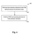
- the method 200 for creating a mask is illustrated by way of example in Fig. 4 .
- the method 200 for creating a mask comprises the step 202 of obtaining mask parameters for a phase shift mask according to any of the device embodiments as described above.
- the mask parameters of the phase shift mask thus are obtained taking into account the dose of the illumination in the lithographic processing for which the phase shift mask will be used.
- the step 202 of obtaining may comprise receiving the necessary mask information or determining, e.g. calculating, measuring and/or deriving, the necessary mask information.
- the step of obtaining may comprise the method 150 of designing a phase shift mask 100 as e.g. described in the first embodiment of the present invention.
- the mask will be generated, using the mask parameters as obtained in step 202.
- a number of different manufacturing steps for the production of the phase shift mask may be introduced.
- Typical method steps for the creation of a phase shift mask may comprise deposition of layers, lithographic processing of layers, etching steps and/or any other suitable construction or treatment step.
- illustration of the mask creation will be provided for a phase shift mask wherein the phase shift of the light stems from the light travelling different optical path lengths in a phase shifting substrate material.
- the method of creating or constructing a phase shift mask 100 according to obtained mask parameter information comprises the step of creating means for generating a phase shift and the step of providing a blocking layer on the substrate in agreement with a pattern to be formed on a device, when the mask is used during lithographic processing.
- Creating means for generating a phase shift may e.g. be creating trenches in a phase shifting substrate.
- the etching depth d etch of the trenches may be determined taking into account the dose or threshold of illumination that will be used on the lithographic system with the phase shift mask 100. The latter may be done by selecting e.g. a specific type of etch or by selecting specific timings for an etch.
- a first example is shown in Fig.
- a substrate 102 typically made of a transparent material such as for example quartz or CaF is coated with a light blocking layer 104, such as e.g. a chrome layer, and coated with a resist layer 222.
- the resist 222 is illuminated according to a pattern, developed and removed, such that no resist is present where no light blocking material is to be present, as shown in Fig. 5b .
- the light blocking material pattern is created by etching light blocking material away according to the resist pattern, as shown in Fig. 5c .
- the remaining resist material 222 may be removed, as shown in Fig. 5d .
- a new resist layer 224 is applied, as shown in Fig. 5e and resist is removed where a trench is to be formed, as shown in Fig. 5f .
- a trench 110 is etched, as shown in Fig. 5g .
- the length of the etching process thereby is determined by the mask parameters provided, thus the etch depth takes into account the dose or threshold for illumination that will be used in the lithographic processing performed with the phase shift mask 100 constructed according to the present embodiment.
- a phase shift mask as shown in Fig. 5h is obtained.
- a substrate 102 typically made of transparent material, is provided with a light blocking layer 104, such as e.g. a chromium layer although the invention is not limited thereto, and a resist layer 222, as shown in Fig. 6a .
- the resist 222 is then selectively removed at places where a trench 110 is to be formed, shown in Fig. 6b , and the light blocking layer 104 is selectively removed, shown in Fig. 6c , whereafter a trench 110 is formed, as can be seen in Fig. 6d .
- the etching of the trench 110 is performed such that for the obtained etch depth or trench depth the dose with which the mask 100 will be illuminated during its use in lithographic processing is taken into account.
- the remaining resist 222 is removed, as shown in Fig. 6e .
- the light blocking layer 104 e.g. chromium layer is patterned using a resist layer 224, as can be seen in Fig. 6f , by selectively removing the resist layer 224, shown in Fig. 6g , subsequently selectively etching the non-covered light blocking layer 104, as shown in Fig. 6h , and by removing the resist layer 224.
- the same phase shift mask 100 as in the previous example is obtained.
- the above examples are only provided by way of illustration and that these are not limiting for the present invention.
- the type of lithography process e.g. type of resist, type of irradiation, etc. and the specific way of forming the means for generating a phase shifting means and for forming the patterned non-blocking layer is not limiting for the present invention.
- Different processes may be known by a person skilled in the art, but in the present invention, during formation of the trench, the etching depth will be determined taking into account the threshold or dose for illumination by which the mask 100 will be irradiated during use in lithographic processing.
- etch depth as a function of the pitch is known, e.g. from Philipsen et al. as referred to above, an adequate dose choice allows to compensate micro-loading errors during mask fabrication.
- the latter also allows obtaining a through-pitch solution to print e.g. 65 nm lines whereby the image imbalance is taken into account.
- lithographic processing comprises covering a device with a resist layer, illuminating said resist layer using the mask, thus providing an illumination pattern on the resist layer and developing said resist in order to obtain a pattern in the resist.
- positive or negative resists may be used in combination with a corresponding mask pattern, as well known by a person skilled in the art.
- the present invention may relate to lithographic processing, whereby the dose of illumination to be used for illuminating the phase shift mask may be determined taking into account the etch depth used for the mask.
- the focus-exposure matrices of the edges of printed features are analysed in order to capture the line displacement due to image imbalance in the process window. It is an advantage that the position of the edges of the feature are evaluated separately, thus allowing an improved lithographic process compared to evaluation of the size of the whole feature.
- the edges 302 of a printed line 304 and the line shift caused by the image imbalance can be taken into account for evaluating image imbalance.
- the feature size e.g. line width
- the position of the edges 302 of the feature 304, e.g. line are taken into account.
- the process windows 320 are determined for each edge 302 and the process window 322 used for evaluating is extracted as the overlapping region of these process windows 320.
- the process window 320 for an edge may be determined in any suitable way, such as e.g. based on obtaining a 10% difference between the design and the obtained structure. Extraction of the processing window 322 for evaluation is illustrated in Fig. 8 , the dashed area indicating the process window for the lithographic processing of the specific feature 304 under study.
- the memory of the memory subsystem 405 may at some time hold part or all (in either case shown as 411) of a set of instructions that when executed on the processing system 400 implement the step(s) of the method embodiments described herein.
- a processing system 400 such as shown in Fig. 9 is prior art
- a system that includes the instructions to implement aspects of the present invention is not prior art, and therefore Fig. 9 is not labelled as
- processor 403 or processors may be a general purpose, or a special purpose processor, and may be for inclusion in a device, e.g., a chip that has other components that perform other functions.
- processors may be implemented in digital electronic circuitry, or in computer hardware, firmware, software, or in combinations of them.
- aspects of the invention can be implemented in a computer program product tangibly embodied in a carrier medium carrying machine-readable code for execution by a programmable processor. Method steps of aspects of the invention may be performed by a programmable processor executing instructions to perform functions of those aspects of the invention, e.g., by operating on input data and generating output data.
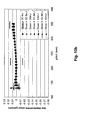
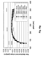
- Fig. 12a and Fig. 12b illustrate the maximum allowed line displacement slope in order to obtain an allowable process window for different pitches.
- a relation between the depth of focus (DOF) at 8% exposure latitude and the line displacement slope is given for a 130 nm pitch and a 220 nm pitch respectively.
- the allowed line displacement slope at 130 nm pitch is 0.007 m/ ⁇ m
- the allowed line displacement slope at 220 nm is 0.015 ⁇ m/ ⁇ m
- the allowed line displacement slope at 350 nm is 0.017 ⁇ m/ ⁇ m.
- the latter may be used in combination with Fig. 10a to Fig. 10g to evaluate for which doses a specific etching depth can be used.
- lithographic processing can be obtained with a large process window for a wide range of pitches, i.e. including for the smallest pitches, allowing lithographic processing not suffering severely from image imbalance.
- the latter is obtained by taking into account the threshold, or taking into account the dose, in the image imbalance compensation optimisation.
Landscapes
- Physics & Mathematics (AREA)
- General Physics & Mathematics (AREA)
- Preparing Plates And Mask In Photomechanical Process (AREA)
- Exposure And Positioning Against Photoresist Photosensitive Materials (AREA)
- Pharmaceuticals Containing Other Organic And Inorganic Compounds (AREA)
- Acyclic And Carbocyclic Compounds In Medicinal Compositions (AREA)
- Control Of Motors That Do Not Use Commutators (AREA)
Claims (13)
- Verfahren (200) zur Herstellung einer Phasenverschiebungsmaske (100) in/auf einem Substrat (102), wobei die Phasenverschiebungsmaske (100) für eine lithografische Bearbeitung einer Vorrichtung unter Verwendung einer vorbestimmten Beleuchtungsdosis geeignet ist, wobei das Verfahren umfasst
Ätzen des Substrats (102) nach Maskenparametern, wobei das Ätzen das Bilden mindestens eines Mittels zum Erzeugen einer Phasenverschiebung (110) umfasst, wobei die Maskenparameter mindestens eine Größe des Mittels zum Erzeugen einer Phasenverschiebung (110) umfassen,
dadurch gekennzeichnet, dass das Verfahren, vor dem Ätzen, das Ändern der Größe des Mittels zum Erzeugen einer Phasenverschiebung (110) unter Berücksichtigung der Beleuchtungsdosis umfasst. - Verfahren (200) nach Anspruch 1, wobei das Ätzen des Substrats (102) das Bilden eines Grabens (110) in dem Substrat (102) umfasst, wobei die Größe des Mittels zum Erzeugen einer Phasenverschiebung (110) mindestens eine Ätztiefe für den Graben (110) ist.
- Verfahren zum Gestalten (150) einer Phasenverschiebungsmaske (100), wobei die Maske (100) mindestens ein Mittel zum Erzeugen einer Phasenverschiebung (110) umfasst, wobei die Maske (100) für eine lithografische Bearbeitung einer Vorrichtung unter Verwendung einer vorbestimmten Beleuchtungsdosis geeignet ist, wobei das Verfahren (150) umfasst
Auswählen eines Satzes von Maskenparametern, umfassend mindestens eine Größe des Mittels zum Erzeugen einer Phasenverschiebung (110),
dadurch gekennzeichnet, dass das Auswählen das Ändern der Größe des Mittels zum Erzeugen einer Phasenverschiebung (110) unter Berücksichtigung der Beleuchtungsdosis umfasst. - Verfahren nach Anspruch 3, wobei das Auswählen eines Satzes von Maskenparametern Folgendes umfasst- Auswählen mehrerer Sätze von Maskenparametern, die geeignet sind, die Phasenverschiebungsmaske (100) im Wesentlichen im Brennpunkt zu verwenden,- Auswählen aus den mehreren Sätzen von Maskenparametern mindestens eines Satzes von Maskenparametern, der zur Verwendung der Phasenverschiebungsmaske (100) mit der Beleuchtungsdosis in einem vorbestimmten Bereich außerhalb des Brennpunkts geeignet ist.
- Verfahren (150) nach einem der Ansprüche 3 bis 4, wobei die Maske (100) mindestens einen Graben (110) und Licht blockierende Teile (104) umfasst, wobei die Maskenparameter mindestens eine Grabenverzerrung, eine Verzerrung des Licht blockierenden Teils und eine Ätztiefe des Grabens umfassen, wobei die Maske zum Drucken von Merkmalen auf einer Vorrichtung geeignet ist, wobei
das Auswählen mehrerer Sätze von Maskenparametern, die zur Verwendung der Phasenverschiebungsmaske (100) im Wesentlichen im Brennpunkt geeignet sind, das Einstellen der Verzerrung des Licht blockierenden Teils umfasst, um eine Merkmalgröße zu korrigieren, und das Einstellen der Grabenverzerrung, um eine Merkmalposition zu korrigieren. - Verfahren (150) nach einem der Ansprüche 3 bis 5, wobei die Maske (100) mindestens eine Graben (110) umfasst und die Maskenparameter mindestens eine Ätztiefe des Grabens (110) umfassen,
wobei das Auswählen des mindestens einen Satzes von Maskenparametern, der zur Verwendung der Phasenverschiebungsmaske (100) mit der Beleuchtungsdosis in einem vorbestimmten Bereich außerhalb des Brennpunkts geeignet ist, das Auswählen eines Satzes von Maskenparametern entsprechend einer vorbestimmten Ätztiefe umfasst. - Verfahren (150) nach einem der Ansprüche 3 bis 6, wobei das Auswählen mindestens eines Satzes von Maskenparametern, der zur Verwendung der Phasenverschiebungsmaske (100) mit der Beleuchtungsdosis in einem vorbestimmten Bereich außerhalb des Brennpunkts geeignet ist, Folgendes umfasst:- Bestimmen eines von einer Brennpunkt-Belichtungsmatrix oder eines Ausmaßes einer Merkmalverschiebung für ein Merkmal, das unter Verwendung der Maske druckbar ist, für die mehreren Sätze von Maskenparametern, und- Auswerten dieses einen von einer Brennpunkt-Belichtungsmatrix oder eines Ausmaßes einer Merkmalverschiebung für ein Merkmal, das unter Verwendung der Maske druckbar ist.
- Verfahren (150) nach einem der Ansprüche 3 bis 7, wobei das Verfahren das Auswerten eines Brennpunkt-Belichtungsfensters (322) für ein Merkmal umfasst, das unter Verwendung der Maske druckbar ist, wobei das Brennpunkt-Belichtungsfenster (322) durch ein gemeinsames Teil von Brennpunkt-Belichtungsfenstern (320) für mindestens zwei Ränder des Merkmals, das unter Verwendung der Maske (100) druckbar ist, bestimmt wird.
- Verfahren durch Durchführung einer lithografischen Bearbeitung einer Vorrichtung, wobei das Verfahren die Verwendung einer Phasenverschiebungsmaske (100) umfasst, umfassend ein Mittel zum Erzeugen einer Phasenverschiebung (110) und unter Verwendung einer Beleuchtungsdosis,
dadurch gekennzeichnet, dass eines von der Phasenverschiebungsmaske (100) und der Beleuchtungsdosis abhängig von dem anderen geändert wird. - Verfahren nach Anspruch 9, wobei für eine vorbestimmte Beleuchtungsdosis die Phasenverschiebungsmaske (100) nach einem der Ansprüche 1 bis 2 hergestellt ist oder die Phasenverschiebungsmaske (100) nach einem der Ansprüche 3 bis 8 gestaltet ist.
- Verfahren nach Anspruch 9, wobei für eine vorbestimmte Phasenverschiebungsmaske (100) eine Beleuchtungsdosis abhängig von Maskenparametern geändert wird, umfassend eine Größe eines Mittels zum Erzeugen einer Phasenverschiebung (110) der Phasenverschiebungsmaske (100).
- Computerprogrammprodukt zum Gestalten einer Phasenverschiebungsmaske nach einem der Ansprüche 3 bis 9.
- Maschinenlesbare Datenspeichervorrichtung, umfassend das Computerprogrammprodukt nach Anspruch 12.
Priority Applications (5)
| Application Number | Priority Date | Filing Date | Title |
|---|---|---|---|
| EP05447222A EP1770439B1 (de) | 2005-10-03 | 2005-10-03 | Alternierende Phasenmaske |
| AT05447222T ATE467149T1 (de) | 2005-10-03 | 2005-10-03 | Alternierende phasenmaske |
| DE602005021106T DE602005021106D1 (de) | 2005-10-03 | 2005-10-03 | Alternierende Phasenmaske |
| JP2006271857A JP5084217B2 (ja) | 2005-10-03 | 2006-10-03 | 交互位相シフトマスク |
| US11/543,302 US7761837B2 (en) | 2005-10-03 | 2006-10-03 | Method of making alternating phase shift masks |
Applications Claiming Priority (1)
| Application Number | Priority Date | Filing Date | Title |
|---|---|---|---|
| EP05447222A EP1770439B1 (de) | 2005-10-03 | 2005-10-03 | Alternierende Phasenmaske |
Publications (2)
| Publication Number | Publication Date |
|---|---|
| EP1770439A1 EP1770439A1 (de) | 2007-04-04 |
| EP1770439B1 true EP1770439B1 (de) | 2010-05-05 |
Family
ID=35482116
Family Applications (1)
| Application Number | Title | Priority Date | Filing Date |
|---|---|---|---|
| EP05447222A Not-in-force EP1770439B1 (de) | 2005-10-03 | 2005-10-03 | Alternierende Phasenmaske |
Country Status (5)
| Country | Link |
|---|---|
| US (1) | US7761837B2 (de) |
| EP (1) | EP1770439B1 (de) |
| JP (1) | JP5084217B2 (de) |
| AT (1) | ATE467149T1 (de) |
| DE (1) | DE602005021106D1 (de) |
Families Citing this family (7)
| Publication number | Priority date | Publication date | Assignee | Title |
|---|---|---|---|---|
| EP1804119A1 (de) * | 2005-12-27 | 2007-07-04 | Interuniversitair Microelektronica Centrum | Verfahren zur Herstellung gedämpfter Phasenverschiebungsmasken und daraus erhaltene Vorrichtungen |
| DE102007031691A1 (de) | 2007-07-06 | 2009-01-08 | Carl Zeiss Smt Ag | Verfahren zum Betreiben einer Mikrolithographischen Projektionsbelichtunganlagen |
| US10534257B2 (en) * | 2017-05-01 | 2020-01-14 | Lam Research Corporation | Layout pattern proximity correction through edge placement error prediction |
| US10572697B2 (en) | 2018-04-06 | 2020-02-25 | Lam Research Corporation | Method of etch model calibration using optical scatterometry |
| KR20200131342A (ko) | 2018-04-10 | 2020-11-23 | 램 리써치 코포레이션 | 레지스트 및 에칭 모델링 |
| WO2019200015A1 (en) | 2018-04-10 | 2019-10-17 | Lam Research Corporation | Optical metrology in machine learning to characterize features |
| US10846574B1 (en) | 2019-07-12 | 2020-11-24 | Electronics For Imaging, Inc. | Variable smoothing in printing |
Family Cites Families (13)
| Publication number | Priority date | Publication date | Assignee | Title |
|---|---|---|---|---|
| JP3339174B2 (ja) * | 1993-11-08 | 2002-10-28 | ソニー株式会社 | フォトマスクの製造方法、露光方法及び半導体装置の製造方法 |
| JP3388986B2 (ja) * | 1996-03-08 | 2003-03-24 | 株式会社東芝 | 露光用マスク及びその製造方法 |
| JP2002072442A (ja) * | 2000-08-30 | 2002-03-12 | Sony Corp | 位相シフトマスクの製造方法、レジストパターンの形成方法および半導体装置の製造方法 |
| JP2002118049A (ja) * | 2000-10-06 | 2002-04-19 | Hitachi Ltd | 半導体集積回路装置の製造方法 |
| TWI252516B (en) * | 2002-03-12 | 2006-04-01 | Toshiba Corp | Determination method of process parameter and method for determining at least one of process parameter and design rule |
| JP4204858B2 (ja) * | 2002-12-11 | 2009-01-07 | 大日本印刷株式会社 | 位相シフトマスクの設計方法および設計装置 |
| JP2005084170A (ja) * | 2003-09-05 | 2005-03-31 | Dainippon Printing Co Ltd | 位相シフトマスクの設計方法/製造方法/設計装置 |
| JP4539061B2 (ja) * | 2003-09-08 | 2010-09-08 | 凸版印刷株式会社 | 位相シフトマスクの製造方法及び位相シフトマスク並びに半導体素子の製造方法 |
| SG111289A1 (en) * | 2003-11-05 | 2005-05-30 | Asml Masktools Bv | A method for performing transmission tuning of a mask pattern to improve process latitude |
| US7646906B2 (en) * | 2004-01-29 | 2010-01-12 | Kla-Tencor Technologies Corp. | Computer-implemented methods for detecting defects in reticle design data |
| JP4351928B2 (ja) * | 2004-02-23 | 2009-10-28 | 株式会社東芝 | マスクデータの補正方法、フォトマスクの製造方法及びマスクデータの補正プログラム |
| US7642019B2 (en) * | 2005-04-15 | 2010-01-05 | Samsung Electronics Co., Ltd. | Methods for monitoring and adjusting focus variation in a photolithographic process using test features printed from photomask test pattern images; and machine readable program storage device having instructions therefore |
| US7536670B2 (en) * | 2005-05-31 | 2009-05-19 | Cadence Design Systems, Inc. | Method for verifying and choosing lithography model |
-
2005
- 2005-10-03 DE DE602005021106T patent/DE602005021106D1/de active Active
- 2005-10-03 AT AT05447222T patent/ATE467149T1/de not_active IP Right Cessation
- 2005-10-03 EP EP05447222A patent/EP1770439B1/de not_active Not-in-force
-
2006
- 2006-10-03 JP JP2006271857A patent/JP5084217B2/ja not_active Expired - Fee Related
- 2006-10-03 US US11/543,302 patent/US7761837B2/en not_active Expired - Fee Related
Also Published As
| Publication number | Publication date |
|---|---|
| JP2007102230A (ja) | 2007-04-19 |
| ATE467149T1 (de) | 2010-05-15 |
| US7761837B2 (en) | 2010-07-20 |
| US20070087273A1 (en) | 2007-04-19 |
| EP1770439A1 (de) | 2007-04-04 |
| JP5084217B2 (ja) | 2012-11-28 |
| DE602005021106D1 (de) | 2010-06-17 |
Similar Documents
| Publication | Publication Date | Title |
|---|---|---|
| US6635393B2 (en) | Blank for alternating PSM photomask with charge dissipation layer | |
| US6830854B2 (en) | System and method for correcting 3D effects in an alternating phase-shifting mask | |
| KR100714480B1 (ko) | 포토마스크의 테스트 패턴 이미지로부터 인쇄된 테스트피쳐들을 이용하는 포토리소그래피 공정에 있어서 초점변화를 측정하는 시스템 및 방법 | |
| EP1770439B1 (de) | Alternierende Phasenmaske | |
| JP4074816B2 (ja) | 分解能向上技術の適用に優先順位を付ける方法及び装置 | |
| KR100763222B1 (ko) | 향상된 포토리소그래피 공정 윈도우를 제공하는 포토마스크구조 및 그 제조 방법 | |
| US6785879B2 (en) | Model-based data conversion | |
| US6794096B2 (en) | Phase shifting mask topography effect correction based on near-field image properties | |
| JP2007535694A (ja) | 透過率を調整することができる埋込減衰型位相シフトマスク | |
| US20070111112A1 (en) | Systems and methods for fabricating photo masks | |
| US6993455B2 (en) | Method for determining the construction of a mask for the micropatterning of semiconductor substrates by means of photolithography | |
| TWI436160B (zh) | 雷文生型相位移光罩及其製造方法 | |
| US7945869B2 (en) | Mask and method for patterning a semiconductor wafer | |
| US7251806B2 (en) | Model-based two-dimensional interpretation filtering | |
| JP5313429B2 (ja) | 光リソグラフィ方法 | |
| US6933084B2 (en) | Alternating aperture phase shift photomask having light absorption layer | |
| KR20070068910A (ko) | 위상 반전 마스크의 임계 치수 보정방법 | |
| US6395432B1 (en) | Methods of determining processing alignment in the forming of phase shift regions | |
| KR20020018077A (ko) | 위상 시프트 마스크의 제조 방법, 레지스트 패턴 형성방법 및 반도체 장치의 제조 방법 | |
| JP2007233138A (ja) | マスク、マスクの製造方法およびそのマスクを用いた半導体装置の製造方法 | |
| US6720114B1 (en) | Method of forming an alternating phase shift circuitry fabrication mask, method of forming a circuitry fabrication mask having a subtractive alternating phase shift region, and alternating phase shift mask | |
| JP4314899B2 (ja) | 位相シフトマスクの製造方法 | |
| JP2002357889A (ja) | 位相シフトマスクの作製装置及び作製方法並びに位相シフトマスクを使用するパターン形成方法 | |
| US20020136962A1 (en) | Method for improving process window in semi-dense area by using phase shifter | |
| JP2008040308A (ja) | フォトマスク、フォトマスクの製造方法、フォトマスクのパターン設計方法および電子デバイスの製造方法 |
Legal Events
| Date | Code | Title | Description |
|---|---|---|---|
| PUAI | Public reference made under article 153(3) epc to a published international application that has entered the european phase |
Free format text: ORIGINAL CODE: 0009012 |
|
| AK | Designated contracting states |
Kind code of ref document: A1 Designated state(s): AT BE BG CH CY CZ DE DK EE ES FI FR GB GR HU IE IS IT LI LT LU LV MC NL PL PT RO SE SI SK TR |
|
| AX | Request for extension of the european patent |
Extension state: AL BA HR MK YU |
|
| 17P | Request for examination filed |
Effective date: 20070912 |
|
| AKX | Designation fees paid |
Designated state(s): AT BE BG CH CY CZ DE DK EE ES FI FR GB GR HU IE IS IT LI LT LU LV MC NL PL PT RO SE SI SK TR |
|
| 17Q | First examination report despatched |
Effective date: 20080407 |
|
| RAP1 | Party data changed (applicant data changed or rights of an application transferred) |
Owner name: IMEC |
|
| GRAP | Despatch of communication of intention to grant a patent |
Free format text: ORIGINAL CODE: EPIDOSNIGR1 |
|
| GRAS | Grant fee paid |
Free format text: ORIGINAL CODE: EPIDOSNIGR3 |
|
| GRAA | (expected) grant |
Free format text: ORIGINAL CODE: 0009210 |
|
| STAA | Information on the status of an ep patent application or granted ep patent |
Free format text: STATUS: THE PATENT HAS BEEN GRANTED |
|
| AK | Designated contracting states |
Kind code of ref document: B1 Designated state(s): AT BE BG CH CY CZ DE DK EE ES FI FR GB GR HU IE IS IT LI LT LU LV MC NL PL PT RO SE SI SK TR |
|
| REG | Reference to a national code |
Ref country code: GB Ref legal event code: FG4D |
|
| REG | Reference to a national code |
Ref country code: CH Ref legal event code: EP |
|
| REG | Reference to a national code |
Ref country code: IE Ref legal event code: FG4D |
|
| REF | Corresponds to: |
Ref document number: 602005021106 Country of ref document: DE Date of ref document: 20100617 Kind code of ref document: P |
|
| REG | Reference to a national code |
Ref country code: NL Ref legal event code: VDEP Effective date: 20100505 |
|
| LTIE | Lt: invalidation of european patent or patent extension |
Effective date: 20100505 |
|
| PG25 | Lapsed in a contracting state [announced via postgrant information from national office to epo] |
Ref country code: LT Free format text: LAPSE BECAUSE OF FAILURE TO SUBMIT A TRANSLATION OF THE DESCRIPTION OR TO PAY THE FEE WITHIN THE PRESCRIBED TIME-LIMIT Effective date: 20100505 Ref country code: NL Free format text: LAPSE BECAUSE OF FAILURE TO SUBMIT A TRANSLATION OF THE DESCRIPTION OR TO PAY THE FEE WITHIN THE PRESCRIBED TIME-LIMIT Effective date: 20100505 Ref country code: ES Free format text: LAPSE BECAUSE OF FAILURE TO SUBMIT A TRANSLATION OF THE DESCRIPTION OR TO PAY THE FEE WITHIN THE PRESCRIBED TIME-LIMIT Effective date: 20100816 Ref country code: SE Free format text: LAPSE BECAUSE OF FAILURE TO SUBMIT A TRANSLATION OF THE DESCRIPTION OR TO PAY THE FEE WITHIN THE PRESCRIBED TIME-LIMIT Effective date: 20100505 |
|
| PG25 | Lapsed in a contracting state [announced via postgrant information from national office to epo] |
Ref country code: IS Free format text: LAPSE BECAUSE OF FAILURE TO SUBMIT A TRANSLATION OF THE DESCRIPTION OR TO PAY THE FEE WITHIN THE PRESCRIBED TIME-LIMIT Effective date: 20100905 Ref country code: FI Free format text: LAPSE BECAUSE OF FAILURE TO SUBMIT A TRANSLATION OF THE DESCRIPTION OR TO PAY THE FEE WITHIN THE PRESCRIBED TIME-LIMIT Effective date: 20100505 Ref country code: AT Free format text: LAPSE BECAUSE OF FAILURE TO SUBMIT A TRANSLATION OF THE DESCRIPTION OR TO PAY THE FEE WITHIN THE PRESCRIBED TIME-LIMIT Effective date: 20100505 Ref country code: SI Free format text: LAPSE BECAUSE OF FAILURE TO SUBMIT A TRANSLATION OF THE DESCRIPTION OR TO PAY THE FEE WITHIN THE PRESCRIBED TIME-LIMIT Effective date: 20100505 Ref country code: LV Free format text: LAPSE BECAUSE OF FAILURE TO SUBMIT A TRANSLATION OF THE DESCRIPTION OR TO PAY THE FEE WITHIN THE PRESCRIBED TIME-LIMIT Effective date: 20100505 |
|
| PG25 | Lapsed in a contracting state [announced via postgrant information from national office to epo] |
Ref country code: PL Free format text: LAPSE BECAUSE OF FAILURE TO SUBMIT A TRANSLATION OF THE DESCRIPTION OR TO PAY THE FEE WITHIN THE PRESCRIBED TIME-LIMIT Effective date: 20100505 Ref country code: GR Free format text: LAPSE BECAUSE OF FAILURE TO SUBMIT A TRANSLATION OF THE DESCRIPTION OR TO PAY THE FEE WITHIN THE PRESCRIBED TIME-LIMIT Effective date: 20100806 Ref country code: CY Free format text: LAPSE BECAUSE OF FAILURE TO SUBMIT A TRANSLATION OF THE DESCRIPTION OR TO PAY THE FEE WITHIN THE PRESCRIBED TIME-LIMIT Effective date: 20100505 |
|
| PG25 | Lapsed in a contracting state [announced via postgrant information from national office to epo] |
Ref country code: DK Free format text: LAPSE BECAUSE OF FAILURE TO SUBMIT A TRANSLATION OF THE DESCRIPTION OR TO PAY THE FEE WITHIN THE PRESCRIBED TIME-LIMIT Effective date: 20100505 Ref country code: PT Free format text: LAPSE BECAUSE OF FAILURE TO SUBMIT A TRANSLATION OF THE DESCRIPTION OR TO PAY THE FEE WITHIN THE PRESCRIBED TIME-LIMIT Effective date: 20100906 Ref country code: EE Free format text: LAPSE BECAUSE OF FAILURE TO SUBMIT A TRANSLATION OF THE DESCRIPTION OR TO PAY THE FEE WITHIN THE PRESCRIBED TIME-LIMIT Effective date: 20100505 |
|
| PG25 | Lapsed in a contracting state [announced via postgrant information from national office to epo] |
Ref country code: BE Free format text: LAPSE BECAUSE OF FAILURE TO SUBMIT A TRANSLATION OF THE DESCRIPTION OR TO PAY THE FEE WITHIN THE PRESCRIBED TIME-LIMIT Effective date: 20100505 Ref country code: CZ Free format text: LAPSE BECAUSE OF FAILURE TO SUBMIT A TRANSLATION OF THE DESCRIPTION OR TO PAY THE FEE WITHIN THE PRESCRIBED TIME-LIMIT Effective date: 20100505 Ref country code: RO Free format text: LAPSE BECAUSE OF FAILURE TO SUBMIT A TRANSLATION OF THE DESCRIPTION OR TO PAY THE FEE WITHIN THE PRESCRIBED TIME-LIMIT Effective date: 20100505 Ref country code: SK Free format text: LAPSE BECAUSE OF FAILURE TO SUBMIT A TRANSLATION OF THE DESCRIPTION OR TO PAY THE FEE WITHIN THE PRESCRIBED TIME-LIMIT Effective date: 20100505 |
|
| PLBE | No opposition filed within time limit |
Free format text: ORIGINAL CODE: 0009261 |
|
| STAA | Information on the status of an ep patent application or granted ep patent |
Free format text: STATUS: NO OPPOSITION FILED WITHIN TIME LIMIT |
|
| PG25 | Lapsed in a contracting state [announced via postgrant information from national office to epo] |
Ref country code: IT Free format text: LAPSE BECAUSE OF FAILURE TO SUBMIT A TRANSLATION OF THE DESCRIPTION OR TO PAY THE FEE WITHIN THE PRESCRIBED TIME-LIMIT Effective date: 20100505 |
|
| 26N | No opposition filed |
Effective date: 20110208 |
|
| REG | Reference to a national code |
Ref country code: DE Ref legal event code: R097 Ref document number: 602005021106 Country of ref document: DE Effective date: 20110207 |
|
| PG25 | Lapsed in a contracting state [announced via postgrant information from national office to epo] |
Ref country code: MC Free format text: LAPSE BECAUSE OF NON-PAYMENT OF DUE FEES Effective date: 20101031 |
|
| REG | Reference to a national code |
Ref country code: CH Ref legal event code: PL |
|
| PG25 | Lapsed in a contracting state [announced via postgrant information from national office to epo] |
Ref country code: LI Free format text: LAPSE BECAUSE OF NON-PAYMENT OF DUE FEES Effective date: 20101031 Ref country code: CH Free format text: LAPSE BECAUSE OF NON-PAYMENT OF DUE FEES Effective date: 20101031 |
|
| PG25 | Lapsed in a contracting state [announced via postgrant information from national office to epo] |
Ref country code: IE Free format text: LAPSE BECAUSE OF NON-PAYMENT OF DUE FEES Effective date: 20101003 |
|
| PG25 | Lapsed in a contracting state [announced via postgrant information from national office to epo] |
Ref country code: LU Free format text: LAPSE BECAUSE OF NON-PAYMENT OF DUE FEES Effective date: 20101003 Ref country code: BG Free format text: LAPSE BECAUSE OF FAILURE TO SUBMIT A TRANSLATION OF THE DESCRIPTION OR TO PAY THE FEE WITHIN THE PRESCRIBED TIME-LIMIT Effective date: 20100505 Ref country code: HU Free format text: LAPSE BECAUSE OF FAILURE TO SUBMIT A TRANSLATION OF THE DESCRIPTION OR TO PAY THE FEE WITHIN THE PRESCRIBED TIME-LIMIT Effective date: 20101106 |
|
| PG25 | Lapsed in a contracting state [announced via postgrant information from national office to epo] |
Ref country code: TR Free format text: LAPSE BECAUSE OF FAILURE TO SUBMIT A TRANSLATION OF THE DESCRIPTION OR TO PAY THE FEE WITHIN THE PRESCRIBED TIME-LIMIT Effective date: 20100505 |
|
| PG25 | Lapsed in a contracting state [announced via postgrant information from national office to epo] |
Ref country code: BG Free format text: LAPSE BECAUSE OF FAILURE TO SUBMIT A TRANSLATION OF THE DESCRIPTION OR TO PAY THE FEE WITHIN THE PRESCRIBED TIME-LIMIT Effective date: 20100805 |
|
| REG | Reference to a national code |
Ref country code: FR Ref legal event code: PLFP Year of fee payment: 12 |
|
| REG | Reference to a national code |
Ref country code: FR Ref legal event code: PLFP Year of fee payment: 13 |
|
| REG | Reference to a national code |
Ref country code: FR Ref legal event code: PLFP Year of fee payment: 14 |
|
| PGFP | Annual fee paid to national office [announced via postgrant information from national office to epo] |
Ref country code: FR Payment date: 20190919 Year of fee payment: 15 |
|
| PGFP | Annual fee paid to national office [announced via postgrant information from national office to epo] |
Ref country code: GB Payment date: 20190923 Year of fee payment: 15 |
|
| PGFP | Annual fee paid to national office [announced via postgrant information from national office to epo] |
Ref country code: DE Payment date: 20190918 Year of fee payment: 15 |
|
| REG | Reference to a national code |
Ref country code: DE Ref legal event code: R119 Ref document number: 602005021106 Country of ref document: DE |
|
| GBPC | Gb: european patent ceased through non-payment of renewal fee |
Effective date: 20201003 |
|
| PG25 | Lapsed in a contracting state [announced via postgrant information from national office to epo] |
Ref country code: FR Free format text: LAPSE BECAUSE OF NON-PAYMENT OF DUE FEES Effective date: 20201031 Ref country code: DE Free format text: LAPSE BECAUSE OF NON-PAYMENT OF DUE FEES Effective date: 20210501 |
|
| PG25 | Lapsed in a contracting state [announced via postgrant information from national office to epo] |
Ref country code: GB Free format text: LAPSE BECAUSE OF NON-PAYMENT OF DUE FEES Effective date: 20201003 |