EP1764797A2 - Herstellungsverfahren für optische Platten - Google Patents
Herstellungsverfahren für optische Platten Download PDFInfo
- Publication number
- EP1764797A2 EP1764797A2 EP06125573A EP06125573A EP1764797A2 EP 1764797 A2 EP1764797 A2 EP 1764797A2 EP 06125573 A EP06125573 A EP 06125573A EP 06125573 A EP06125573 A EP 06125573A EP 1764797 A2 EP1764797 A2 EP 1764797A2
- Authority
- EP
- European Patent Office
- Prior art keywords
- stamper
- electrode
- thin film
- forming
- resist film
- Prior art date
- Legal status (The legal status is an assumption and is not a legal conclusion. Google has not performed a legal analysis and makes no representation as to the accuracy of the status listed.)
- Withdrawn
Links
Images




Classifications
-
- G—PHYSICS
- G11—INFORMATION STORAGE
- G11B—INFORMATION STORAGE BASED ON RELATIVE MOVEMENT BETWEEN RECORD CARRIER AND TRANSDUCER
- G11B7/00—Recording or reproducing by optical means, e.g. recording using a thermal beam of optical radiation by modifying optical properties or the physical structure, reproducing using an optical beam at lower power by sensing optical properties; Record carriers therefor
- G11B7/24—Record carriers characterised by shape, structure or physical properties, or by the selection of the material
- G11B7/26—Apparatus or processes specially adapted for the manufacture of record carriers
- G11B7/263—Preparing and using a stamper, e.g. pressing or injection molding substrates
-
- C—CHEMISTRY; METALLURGY
- C25—ELECTROLYTIC OR ELECTROPHORETIC PROCESSES; APPARATUS THEREFOR
- C25D—PROCESSES FOR THE ELECTROLYTIC OR ELECTROPHORETIC PRODUCTION OF COATINGS; ELECTROFORMING; APPARATUS THEREFOR
- C25D1/00—Electroforming
- C25D1/10—Moulds; Masks; Masterforms
-
- G—PHYSICS
- G11—INFORMATION STORAGE
- G11B—INFORMATION STORAGE BASED ON RELATIVE MOVEMENT BETWEEN RECORD CARRIER AND TRANSDUCER
- G11B7/00—Recording or reproducing by optical means, e.g. recording using a thermal beam of optical radiation by modifying optical properties or the physical structure, reproducing using an optical beam at lower power by sensing optical properties; Record carriers therefor
- G11B7/24—Record carriers characterised by shape, structure or physical properties, or by the selection of the material
- G11B7/26—Apparatus or processes specially adapted for the manufacture of record carriers
- G11B7/261—Preparing a master, e.g. exposing photoresist, electroforming
-
- G—PHYSICS
- G11—INFORMATION STORAGE
- G11B—INFORMATION STORAGE BASED ON RELATIVE MOVEMENT BETWEEN RECORD CARRIER AND TRANSDUCER
- G11B2220/00—Record carriers by type
- G11B2220/20—Disc-shaped record carriers
- G11B2220/25—Disc-shaped record carriers characterised in that the disc is based on a specific recording technology
- G11B2220/2537—Optical discs
-
- Y—GENERAL TAGGING OF NEW TECHNOLOGICAL DEVELOPMENTS; GENERAL TAGGING OF CROSS-SECTIONAL TECHNOLOGIES SPANNING OVER SEVERAL SECTIONS OF THE IPC; TECHNICAL SUBJECTS COVERED BY FORMER USPC CROSS-REFERENCE ART COLLECTIONS [XRACs] AND DIGESTS
- Y10—TECHNICAL SUBJECTS COVERED BY FORMER USPC
- Y10S—TECHNICAL SUBJECTS COVERED BY FORMER USPC CROSS-REFERENCE ART COLLECTIONS [XRACs] AND DIGESTS
- Y10S425/00—Plastic article or earthenware shaping or treating: apparatus
- Y10S425/81—Sound record
Definitions
- the present invention relates to a thin film for stamper formation, formed on the surface of a patterned resist material, to be used as an electrode for electrocasting of a stamper material, and an electrode material for stamper formation to be used as the material for such an electrode.
- FIGS. 8A to 8F show a conventional stamper production method.
- a photoresist film 102 is formed on a glass substrate 101 by spin coating, or the like.
- the photo resist film 102 is exposed by a laser beam so as to form a latent image 102a.
- a pattern having a groove part 102b as shown in FIG. 8C is formed.
- FIG. 8C shows a pattern having a groove part 102b as shown in FIG. 8C .
- a nickel thin film 103 is formed on the surface of the photo resist film 102 and the glass substrate 101 by a sputtering method, a vapor deposition method, or the like. Thereafter, as shown in FIG. 8E, by applying a nickel electrocasting on the nickel thin film 103 surface, using the nickel thin film 103 as an electrode, a nickel layer 104 is formed. As shown in FIG. 8F, after peeling off the nickel layer 104 from the glass substrate 101, by polishing the upper surface of the nickel layer 104, or the like in FIG. 8F, a stamper 104A can be obtained.
- a higher recording density is further required to the optical discs.
- the expected demand of a high recording density for ensuring a recording capacity of as much as a several tens of GB or more in a 12 cm diameter disc cannot be dealt with by the above-mentioned laser cutting using a laser beam, and thus an electron beam cutting using an electron beam attracts the attention as a method instead of the laser beam cutting.
- the electron beam cutting a highly fine pattern can be formed compared with the conventional laser beam cutting.
- the electron absorption sensitivity of the resist material should be improved, and thus an electron attractive group such as a chlorine, a sulfur, and a fluorine, or the like is introduced into the resist material.
- an electron attractive group such as a chlorine, a sulfur, and a fluorine, or the like is introduced into the resist material.
- a problem of the stamper quality deterioration arises by the damage of the nickel thin film due to reaction of the electron attractive group in the resist material and the nickel thin film at the time of applying the nickel electrocasting.
- an object of the present invention is to provide a production method for an optical disc, capable of obtaining a good S/N ratio without deterioration of the stamper quality due to reaction with an electron attractive group contained in a resist material.
- a production method for an optical disc comprises the processes of forming a resist film on a substrate, patterning the resist film on the substrate by an electron beam cutting, forming an electrode on the patterned resist film, forming a metal layer on the electrode by the electrocasting, and injection molding of a resin, using the metal layer peeled off from the electrode as a stamper, wherein the electrode contains Ni element as the main component as well as Ru element by less than 25% by weight.
- the stamper quality deterioration can be prevented.
- the electrode can be formed with the excellent flatness, the S/N ratio of the optical disc can be improved.
- a production method for an optical disc comprises the processes of forming a resist film on a substrate, patterning the resist film on the substrate by an electron beam cutting, forming an electrode on the patterned resist film, forming a metal layer on the electrode by the electrocasting, and injection molding of a resin, using the metal layer peeled off from the electrode as a stamper, wherein the electrode contains Ni element as the main component as well as Cu element by less than 25% by weight.
- a production method for an optical disc comprises the processes of forming a resist film on a substrate, patterning the resist film on the substrate by an electron beam cutting, forming an electrode on the patterned resist film, forming a metal layer on the electrode by the electrocasting, and injection molding of a resin, using the metal layer peeled off from the electrode as a stamper, wherein the electrode contains Ni element as the main component as well as P element by less than 25% by weight.
- a production method for an optical disc comprises the processes of forming a resist film on a substrate, patterning the resist film on the substrate by an electron beam cutting, forming an electrode on the patterned resist film, forming a metal layer on the electrode by the electrocasting, and injection molding of a resin, using the metal layer peeled off from the electrode as a stamper, wherein the electrode contains Ni element as the main component as well as Mg element by less than 25% by weight.
- a production method for an optical disc comprises the processes of forming a resist film on a substrate, patterning the resist film on the substrate by an electron beam cutting, forming an electrode on the patterned resist film, forming a metal layer on the electrode by the electrocasting, and injection molding of a resin, using the metal layer peeled off from the electrode as a stamper, wherein the electrode contains Ni element as the main component as well as Cr element by less than 25% by weight.
- the stamper quality deterioration can be prevented.
- the electrode can be formed with the excellent flatness, the S/N ratio of the optical disc can be improved.
- a production method for an optical disc comprises the processes of forming a resist film on a substrate, patterning the resist film on the substrate by an electron beam cutting, forming an electrode on the patterned resist film, forming a metal layer on the electrode by the electrocasting, and injection molding of a resin, using the metal layer peeled off from the electrode as a stamper, wherein the electrode contains Ni element as the main component as well as Au element by less than 25% by weight.
- a production method for an optical disc according to the present invention comprises the processes of forming a res ist film on a substrate, patterning the resist film on the substrate by an electron beam cutting, forming an electrode on the patterned resist film, forming a metal layer on the electrode by the electrocasting, and injection molding of a resin, using the metal layer peeled off from the electrode as a stamper, wherein the electrode contains Ni element as the main component as well as Si element by less than 25% by weight.
- a production method for an optical disc comprises the processes of forming a resist film on a substrate, patterning the resist film on the substrate by an electron beam cutting, forming an electrode on the patterned resist film, forming a metal layer on the electrode by the electrocasting, and injection molding of a resin, using the metal layer peeled off from the electrode as a stamper, wherein the electrode contains Ni element as the main component as well as Ti element by less than 50% by weight.
- a production method for an optical disc comprises the processes of forming a resist film on a substrate, patterning the resist film on the substrate by an electron beam cutting, forming an electrode on the patterned resist film, forming a metal layer on the electrode by the electrocasting, and injection molding of a resin, using the metal layer peeled off from the electrode as a stamper, wherein the electrode contains Ni element as the main component as well as Ag element by less than 50% by weight.
- the stamper quality deterioration can be prevented.
- the electrode can be formed with the excellent flatness, the S/N ratio of the optical disc can be improved.
- the metal layer can be made of nickel. Moreover, the metal layer can also be made of nickel alloy.
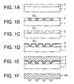
- FIGS. 1A to 1F are cross-sectional views showing processes for producing a stamper for the optical disc production
- FIG. 2 is a chart showing the details of the processes.
- an electron beam resist film 2 is produced for an electron beam on the glass substrate 1 by spin coating, or the like.
- the electron beam resist film 2 is pre-baked, and the electron beam resist film 2 is exposed by an electron beam so as to form a latent image 2a as shown in FIG. 1B ("signal recording" in FIG. 2).
- the electron beam resist film 2 is developed for forming a groove part 2b as shown in FIG. 1C, and the electron beam resist film 2 is post-baked.
- a nickel alloy thin film 3 is formed on the surface of the electron beam resist film 2 and the glass substrate 1 by a sputtering method, a deposition method, or an electroless plating.
- the material of the nickel alloy thin film will be described later.
- a nickel layer 4 is formed.
- a master stamper 4A is obtained by polishing the upper surface of the nickel layer 4 of FIG. 1F, or the like. It is possible to form a nickel alloy layer by electrocasting in stead of the nickel layer 4, and use the peeled-off nickel alloy layer as the stamper.
- a sub master stamper can be obtained with the shape reversed.
- a baby stamper can be obtained with the same shape as the master stamper. It is also possible to further transfer the baby stamper shape for producing a new stamper.
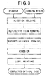
- FIG. 3 is a chart showing processes for producing an optical disc, using the master stamper 4A or a baby stamper. As shown in FIG. 3, after injection molding using a stamper as the mold, a reflection film, a protection film, and the like are formed so as to produce an optical disc. Since the processes in FIG. 3 are the same as ordinary production processes, detailed explanation is not given.
- the nickel alloy thin film 3 by forming the nickel alloy thin film 3 using a Ni alloy with the above-mentioned elements added, damage of the nickel alloy thin film 3 can be prevented at the time of forming the nickel layer 4 by electrocasting.
- the surface oxide film precipitated on the thin film surface thereby becomes a non-conductor so as to serve as a barrier material with respect to the reaction of an external active metal or non-metal and Ni and improves the weather resistance of the Ni alloy.
- P, Mg or Si as an element to be added is easily coupled not only with the oxygen but also with the other active non-metal elements at the same time, in the case it is added by an excessive amount, the weather resistance is inversely lowered. Therefore, an amount less than 20% by weight is considered to be appropriate.
- the Ti is precipitated on the Ni particle grain boundary except the case of forming a compound by the reaction while heating under a high temperature atmosphere. It is considered that although a non-conductor is not formed in the Ni alloy with Ti added, since the Ti is stable with respect to chlorine, the effect of restraining leaching of active elements to the Ni particles or the chemical reaction can be provided, and thus the chemical reaction with respect to the Ni particles can be prevented.
- an alloy thin film with at least one selected from the group consisting of Ru, Ag, and Cr added to Ni not only improves the chlorine resistance but also improves the flatness of the thin film.
- the thin film flattening is confirmed by the signal characteristic at the time of reproduction of an optical disc produced using a stamper formed with the alloy thin film.
- Ru, Ag, or Cr is solidly dissolved, it is confirmed that the crystal lattice of Ni as the main component is distorted so that the thin film grains are made finer.
- the grain growth of the solidly dissolved Ni solid solution alloy particles can be restrained as well as the addition component not solidly dissolved of the added element existing in the grain boundary is considered to have an effect of promoting the stress alleviation.
- the nickel alloy with the composition described in this embodiment has chlorination resistance and bromination resistance while having a spreading property and a processability like the pure Ni, and thus it can be adopted to an application conventionally restricted, or to an applied technology due to the nature of the pure Ni, which can easily be reacted with chlorine and boron.
- Ni and sputtering targets of additive metals Ru, Cu, P, Mg, Cr, Au, Si, Ti, and Ag the sputtering target of specified element and Ni were put in an RF magnetron sputtering apparatus, and a thin film was formed on a quartz substrate.
- the sputtering target was 3 inches (7.62 cm) in diameter, and 5 mm in thickness, and the distance from the sputtering target to the substrate was about 90 mm. While controlling the discharge amount of metal atoms by RF feed power to Ni and sputtering target of specified element, two metals were stacked up on the substrate simultaneously.
- the final degree of vacuum is 3 x 10 -5 Pa and the gas pressure when forming film is 0.7 to 1 Pa.
- the RF feed power was varied in a range of 100 to 500 W depending on the composition of the alloy.
- Ni-Si alloy, Ni-Ti alloy, and Ni-Ag alloy were formed on substrates.
- the content of Ru, Cu, P. Mg, Cr, Au, Si, Ti, and Ag was varied in five concentrations, 1, 5, 10, 20, and 25 percent by weight.
- a pure Ni thin film was formed on the substrate by using the same apparatus (see Fig. 4 and Fig. 5).
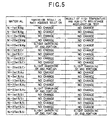
- the quartz substrates having the thin films stacked up thereon by the above method were immersed in sodium chloride aqueous solution and let stand for a specified time, and observed changes with time are shown in Fig. 4 and Fig. 5.
- the sodium chloride contained in the sodium chloride aqueous solution is 5 percent by volume, and the quartz substrates were immersed in the aqueous solution for about 96 hours at ordinary temperature without heating. After standing for 96 hours, changes with time of the thin film were visually observed, and the optical characteristics such as reflectivity of thin film were inspected by spectrophotometer, and changes of surface state of thin films were evaluated.
- Ni-Ru alloy Ni-Cu alloy, Ni-P alloy, Ni-Mg alloy, Ni-Cr alloy, Ni-Au alloy, Ni-Si alloy, Ni-Ti alloy, and Ni-Ag alloy
- Ni-25 wt.% Ru Ni-25 wt.% Cu, Ni-25 wt.% Mg, Ni-25 wt.% Cr, Ni-25 wt.% Au, and Ni-25 wt.% Si
- Ni-25 wt.% Ru, Ni-25 wt.% Cu, Ni-25 wt.% Mg, Ni-25 wt.% Cr, Ni-25 wt.% Au, and Ni-25 wt.% Si as a result of immersion in sodium chloride aqueous solution, a slight darkening in the end portion was noted. No change was observed in other alloy thin films.
- Ni-20 wt.% Ru, Ni-25 wt.% Ru, Ni-20 wt.% Cu, Ni-25 wt.% Cu, Ni-20 wt.% P, Ni-25 wt.% P, Ni-25 wt.% Cr, and Ni-25 wt.% Si as a result of high temperature and humidity resistance acceleration test, a slight darkening in the end portion was noted.
- Fig. 6 is a diagram showing a disk noise measuring method by a mirror section reproduced signal of an optical disk
- Fig. 7 is a diagram showing results of measurement.
- a resist layer 12 is formed on a glass substrate 11, and thin films 13 of pure Ni and Ni- 5 wt.% Ru are formed thereon as electrode materials, and mother disks for measurement were prepared.
- the mother disk for measurement was rotated at linear velocity of 3 m/ s and irradiated with light beam through a lens 14 from the side of the glass substrate 11, and the reflected light from the interface of the resist layer 12 and thin film 13 was received.
- the level of 1 MHz component was measured as noise component, and the result is shown in Fig. 7.
- the disk noise is -74.3 dB in the case of using pure Ni as the material for the thin film 13
- the disk noise is -79.7 dB in the case of using Ni-5 wt.% Ru as the material for the thin film 13. Therefore, in the case of Ni-5 wt.% RU, the S/N ratio is improved by more than 5 dB as compared with the case of pure N1. This result suggests that the flatness of the thin film of Ni-5 wt.% RU is superior to that of the pure Ni, showing excellent suitability as the material used in manufacture of optical mother disk.
- Injection molding of a resin, using a metal layer peeled off from an electrode as a stamper is a concept including the case of producing a new stamper (baby stamper, or the like) from a metal layer (master stamper) peeled off from an electrode, and executing injection molding of a resin, using the new stamper as shown in FIG. 2.
Landscapes
- Engineering & Computer Science (AREA)
- Manufacturing & Machinery (AREA)
- Chemical & Material Sciences (AREA)
- Chemical Kinetics & Catalysis (AREA)
- Electrochemistry (AREA)
- Materials Engineering (AREA)
- Metallurgy (AREA)
- Organic Chemistry (AREA)
- Manufacturing Optical Record Carriers (AREA)
- Moulds For Moulding Plastics Or The Like (AREA)
Applications Claiming Priority (2)
| Application Number | Priority Date | Filing Date | Title |
|---|---|---|---|
| JP2000139385A JP4050859B2 (ja) | 2000-05-12 | 2000-05-12 | スタンパの製造方法及び光ディスクの製造方法 |
| EP01111579A EP1154421A3 (de) | 2000-05-12 | 2001-05-11 | Verfahren zur Herstellung einer optische Platte |
Related Parent Applications (1)
| Application Number | Title | Priority Date | Filing Date |
|---|---|---|---|
| EP01111579A Division EP1154421A3 (de) | 2000-05-12 | 2001-05-11 | Verfahren zur Herstellung einer optische Platte |
Publications (2)
| Publication Number | Publication Date |
|---|---|
| EP1764797A2 true EP1764797A2 (de) | 2007-03-21 |
| EP1764797A3 EP1764797A3 (de) | 2008-11-19 |
Family
ID=18646840
Family Applications (2)
| Application Number | Title | Priority Date | Filing Date |
|---|---|---|---|
| EP06125573A Withdrawn EP1764797A3 (de) | 2000-05-12 | 2001-05-11 | Herstellungsverfahren für optische Platten |
| EP01111579A Withdrawn EP1154421A3 (de) | 2000-05-12 | 2001-05-11 | Verfahren zur Herstellung einer optische Platte |
Family Applications After (1)
| Application Number | Title | Priority Date | Filing Date |
|---|---|---|---|
| EP01111579A Withdrawn EP1154421A3 (de) | 2000-05-12 | 2001-05-11 | Verfahren zur Herstellung einer optische Platte |
Country Status (7)
| Country | Link |
|---|---|
| US (1) | US6695987B2 (de) |
| EP (2) | EP1764797A3 (de) |
| JP (1) | JP4050859B2 (de) |
| KR (1) | KR100597554B1 (de) |
| CN (1) | CN1174403C (de) |
| HK (1) | HK1044618B (de) |
| TW (1) | TW509938B (de) |
Families Citing this family (7)
| Publication number | Priority date | Publication date | Assignee | Title |
|---|---|---|---|---|
| US7066234B2 (en) | 2001-04-25 | 2006-06-27 | Alcove Surfaces Gmbh | Stamping tool, casting mold and methods for structuring a surface of a work piece |
| JP3656591B2 (ja) * | 2001-06-28 | 2005-06-08 | ソニー株式会社 | 光学記録媒体製造用スタンパの製造方法および光学記録媒体の製造方法 |
| TW590999B (en) * | 2002-08-28 | 2004-06-11 | Alliance Fiber Optic Prod Inc | Mold for producing array optical fiber substrate with V-shaped grooves and method for producing the same |
| EP1617428A4 (de) * | 2003-04-18 | 2008-08-20 | Pioneer Corp | Stanzer und herstellungsverfahren dafür |
| US20050221112A1 (en) * | 2004-03-31 | 2005-10-06 | Daewoong Suh | Microtools for package substrate patterning |
| JP2009277335A (ja) * | 2008-04-18 | 2009-11-26 | Fujifilm Corp | スタンパの製造方法およびスタンパを用いた光情報記録媒体の製造方法 |
| CN102016651B (zh) * | 2008-06-06 | 2013-05-22 | 夏普株式会社 | 防反射膜和具备防反射膜的光学元件、压模和压模的制造方法以及防反射膜的制造方法 |
Family Cites Families (21)
| Publication number | Priority date | Publication date | Assignee | Title |
|---|---|---|---|---|
| JPS5835742A (ja) * | 1981-08-21 | 1983-03-02 | Victor Co Of Japan Ltd | 情報記録媒体円盤の製作に用いられるスタンパの製作法 |
| JPS58150148A (ja) * | 1982-02-22 | 1983-09-06 | Toshiba Corp | スタンパ−の製造方法 |
| JPS59193560A (ja) * | 1983-04-19 | 1984-11-02 | Daicel Chem Ind Ltd | 回転記録体用スタンパ−及びその製造法 |
| JPS59222593A (ja) * | 1983-05-31 | 1984-12-14 | Toshiba Corp | 成形用金型の製造方法 |
| JPS61214247A (ja) * | 1985-03-20 | 1986-09-24 | Hitachi Maxell Ltd | 記録媒体用スタンパの製造方法 |
| JP2646533B2 (ja) * | 1986-10-22 | 1997-08-27 | セイコーエプソン株式会社 | 光メモリー用スタンパの製造方法 |
| JPS63112841A (ja) * | 1986-10-28 | 1988-05-17 | Seiko Epson Corp | 光デイスク用スタンパの製造方法 |
| JPS63253551A (ja) * | 1987-04-09 | 1988-10-20 | Seiko Epson Corp | 光デイスクマスタリングプロセスにおける導体化膜 |
| JPS63266058A (ja) * | 1987-04-24 | 1988-11-02 | Seiko Epson Corp | 光デイスク用スタンパの製造方法 |
| JPH01251448A (ja) * | 1988-03-31 | 1989-10-06 | Toshiba Corp | 光ディスク成形金型 |
| JPH02292028A (ja) * | 1989-05-01 | 1990-12-03 | Hitachi Maxell Ltd | 光デイスク用スタンパ |
| EP0488239B1 (de) * | 1990-11-28 | 1997-07-30 | Sharp Kabushiki Kaisha | Herstellungsverfahren einer Matrize |
| US5756130A (en) * | 1993-05-20 | 1998-05-26 | Hitaci Maxell, Ltd. | Stamper for producing recording medium |
| DE69404937T2 (de) * | 1993-09-20 | 1998-01-15 | Mitsubishi Materials Corp | Nickellegierung |
| DE19612329A1 (de) * | 1996-03-28 | 1997-10-02 | Leybold Ag | Verfahren zur Herstellung einer zum Einsetzen in eine Spritzgießform bestimmten Masterabformung |
| US5851251A (en) * | 1996-05-17 | 1998-12-22 | Victor Company Of Japan, Ltd. | Manufacturing methods of optical disc and blank master |
| JPH10312584A (ja) * | 1997-05-12 | 1998-11-24 | Toshiba Emi Ltd | ディスク用金属原盤の製造方法 |
| US6207247B1 (en) * | 1998-03-27 | 2001-03-27 | Nikon Corporation | Method for manufacturing a molding tool used for sustrate molding |
| JPH11333884A (ja) * | 1998-03-27 | 1999-12-07 | Nikon Corp | スタンパ―の製造方法 |
| JPH11328748A (ja) * | 1998-05-19 | 1999-11-30 | Tdk Corp | ディスク原盤 |
| JP3686573B2 (ja) * | 2000-05-12 | 2005-08-24 | パイオニア株式会社 | スタンパ形成用電極材料およびスタンパ形成用薄膜 |
-
2000
- 2000-05-12 JP JP2000139385A patent/JP4050859B2/ja not_active Expired - Fee Related
-
2001
- 2001-05-11 EP EP06125573A patent/EP1764797A3/de not_active Withdrawn
- 2001-05-11 TW TW090111252A patent/TW509938B/zh not_active IP Right Cessation
- 2001-05-11 EP EP01111579A patent/EP1154421A3/de not_active Withdrawn
- 2001-05-11 KR KR1020010025864A patent/KR100597554B1/ko not_active Expired - Fee Related
- 2001-05-12 CN CNB011169184A patent/CN1174403C/zh not_active Expired - Fee Related
- 2001-05-14 US US09/853,676 patent/US6695987B2/en not_active Expired - Fee Related
-
2002
- 2002-08-20 HK HK02106089.7A patent/HK1044618B/zh not_active IP Right Cessation
Also Published As
| Publication number | Publication date |
|---|---|
| TW509938B (en) | 2002-11-11 |
| JP2001319381A (ja) | 2001-11-16 |
| JP4050859B2 (ja) | 2008-02-20 |
| HK1044618A1 (en) | 2002-10-25 |
| US6695987B2 (en) | 2004-02-24 |
| KR100597554B1 (ko) | 2006-07-06 |
| HK1044618B (zh) | 2005-07-15 |
| EP1154421A3 (de) | 2006-06-07 |
| CN1338739A (zh) | 2002-03-06 |
| EP1764797A3 (de) | 2008-11-19 |
| US20010050444A1 (en) | 2001-12-13 |
| KR20010104288A (ko) | 2001-11-24 |
| CN1174403C (zh) | 2004-11-03 |
| EP1154421A2 (de) | 2001-11-14 |
Similar Documents
| Publication | Publication Date | Title |
|---|---|---|
| JP3088168B2 (ja) | 光記録媒体およびその製造方法 | |
| US6695987B2 (en) | Production method for optical disc | |
| KR100597553B1 (ko) | 스탬퍼 형성용 전극 재료 및 스탬퍼 형성용 박막 | |
| HK1099118A (en) | Production method for optical disc | |
| EP1229152B1 (de) | Verwendung eines matrizenformenden Elektrodenmaterials, Verwendung einer matrizenformenden Dünnschicht und Verfahren zur Herstellung optischer Platten | |
| US6849390B2 (en) | Stamper-forming electrode material, stamper-forming thin film, and method of manufacturing optical disk | |
| EP1643497A1 (de) | Optischer aufzeichnungsdatenträger | |
| CN100547664C (zh) | 光记录介质 | |
| JP4755680B2 (ja) | 光情報記録媒体およびその製造方法 | |
| JP4431287B2 (ja) | 光ディスクの製造方法 | |
| JP2002230848A (ja) | スタンパ形成用電極材料及びスタンパ形成用薄膜 | |
| JP4431286B2 (ja) | スタンパ形成用電極材料及びスタンパ形成用薄膜 | |
| JPH08315418A (ja) | 光記録媒体及びその製造方法 | |
| JPS62127286A (ja) | 光記録材料 | |
| JP2002230849A (ja) | 光ディスクの製造方法 | |
| JPH05339774A (ja) | スタンパ製造方法 | |
| JP2006028537A (ja) | 光ディスク用保護膜、保護膜形成用スパッタリングターゲットおよび該スパッタリングターゲットの製造方法 | |
| JP2973990B2 (ja) | 光記録媒体の製造方法 | |
| JP2009093725A (ja) | 光情報記録媒体 | |
| JPH06267117A (ja) | 光ディスク用原盤の製造方法 | |
| JP2009205748A (ja) | 光ディスク用原盤の製造方法及びそれを用いた光ディスクの製造方法 | |
| JPH03171445A (ja) | 情報記録媒体の製造方法 |
Legal Events
| Date | Code | Title | Description |
|---|---|---|---|
| PUAI | Public reference made under article 153(3) epc to a published international application that has entered the european phase |
Free format text: ORIGINAL CODE: 0009012 |
|
| AC | Divisional application: reference to earlier application |
Ref document number: 1154421 Country of ref document: EP Kind code of ref document: P |
|
| AK | Designated contracting states |
Kind code of ref document: A2 Designated state(s): AT BE CH CY DE DK ES FI FR GB GR IE IT LI LU MC NL PT SE TR |
|
| AX | Request for extension of the european patent |
Extension state: AL BA HR MK YU |
|
| RIN1 | Information on inventor provided before grant (corrected) |
Inventor name: UENO, TAKASHIFURUYA METAL CO.,LTD. Inventor name: IIDA, TETSUYAPIONEER CORP. Inventor name: KATSUMURA, MASAHIROPIONEER CORP. |
|
| RIC1 | Information provided on ipc code assigned before grant |
Ipc: C25D 1/10 20060101ALI20070530BHEP Ipc: G11B 7/26 20060101AFI20070215BHEP |
|
| REG | Reference to a national code |
Ref country code: HK Ref legal event code: DE Ref document number: 1099118 Country of ref document: HK |
|
| RIN1 | Information on inventor provided before grant (corrected) |
Inventor name: UENO, TAKASHIFURUYA METAL CO.,LTD. Inventor name: IIDA, TETSUYAPIONEER CORP. Inventor name: KATSUMURA, MASAHIROPIONEER CORP. |
|
| PUAL | Search report despatched |
Free format text: ORIGINAL CODE: 0009013 |
|
| AK | Designated contracting states |
Kind code of ref document: A3 Designated state(s): AT BE CH CY DE DK ES FI FR GB GR IE IT LI LU MC NL PT SE TR |
|
| AX | Request for extension of the european patent |
Extension state: AL BA HR MK RS |
|
| 17P | Request for examination filed |
Effective date: 20090519 |
|
| AKX | Designation fees paid |
Designated state(s): DE FR GB |
|
| 17Q | First examination report despatched |
Effective date: 20101203 |
|
| RAP1 | Party data changed (applicant data changed or rights of an application transferred) |
Owner name: FURUYA METAL CO., LTD. Owner name: PIONEER CORPORATION |
|
| STAA | Information on the status of an ep patent application or granted ep patent |
Free format text: STATUS: THE APPLICATION IS DEEMED TO BE WITHDRAWN |
|
| 18D | Application deemed to be withdrawn |
Effective date: 20110414 |
|
| REG | Reference to a national code |
Ref country code: HK Ref legal event code: WD Ref document number: 1099118 Country of ref document: HK |