EP1758176A1 - Anschlussbox für ein solarzellenmodul - Google Patents
Anschlussbox für ein solarzellenmodul Download PDFInfo
- Publication number
- EP1758176A1 EP1758176A1 EP05741410A EP05741410A EP1758176A1 EP 1758176 A1 EP1758176 A1 EP 1758176A1 EP 05741410 A EP05741410 A EP 05741410A EP 05741410 A EP05741410 A EP 05741410A EP 1758176 A1 EP1758176 A1 EP 1758176A1
- Authority
- EP
- European Patent Office
- Prior art keywords
- diodes
- terminal
- terminal boards
- box
- solar cell
- Prior art date
- Legal status (The legal status is an assumption and is not a legal conclusion. Google has not performed a legal analysis and makes no representation as to the accuracy of the status listed.)
- Withdrawn
Links
- 230000002265 prevention Effects 0.000 claims abstract description 20
- 230000005855 radiation Effects 0.000 claims description 2
- 238000010438 heat treatment Methods 0.000 abstract 1
- 238000005476 soldering Methods 0.000 description 8
- 229920005989 resin Polymers 0.000 description 5
- 239000011347 resin Substances 0.000 description 5
- 230000000694 effects Effects 0.000 description 4
- 238000010248 power generation Methods 0.000 description 4
- 239000004721 Polyphenylene oxide Substances 0.000 description 3
- 239000004020 conductor Substances 0.000 description 3
- 230000007423 decrease Effects 0.000 description 3
- 239000000463 material Substances 0.000 description 3
- 229920001955 polyphenylene ether Polymers 0.000 description 3
- 229920006380 polyphenylene oxide Polymers 0.000 description 3
- 230000008646 thermal stress Effects 0.000 description 3
- 229910001369 Brass Inorganic materials 0.000 description 1
- XUIMIQQOPSSXEZ-UHFFFAOYSA-N Silicon Chemical compound [Si] XUIMIQQOPSSXEZ-UHFFFAOYSA-N 0.000 description 1
- 239000002390 adhesive tape Substances 0.000 description 1
- 239000010951 brass Substances 0.000 description 1
- 210000000078 claw Anatomy 0.000 description 1
- 238000010276 construction Methods 0.000 description 1
- 230000003247 decreasing effect Effects 0.000 description 1
- 238000010586 diagram Methods 0.000 description 1
- 238000009826 distribution Methods 0.000 description 1
- 238000004519 manufacturing process Methods 0.000 description 1
- 238000003825 pressing Methods 0.000 description 1
- 229910052710 silicon Inorganic materials 0.000 description 1
- 239000010703 silicon Substances 0.000 description 1
- 229910000679 solder Inorganic materials 0.000 description 1
- 238000003466 welding Methods 0.000 description 1
Images


Classifications
-
- H—ELECTRICITY
- H02—GENERATION; CONVERSION OR DISTRIBUTION OF ELECTRIC POWER
- H02S—GENERATION OF ELECTRIC POWER BY CONVERSION OF INFRARED RADIATION, VISIBLE LIGHT OR ULTRAVIOLET LIGHT, e.g. USING PHOTOVOLTAIC [PV] MODULES
- H02S40/00—Components or accessories in combination with PV modules, not provided for in groups H02S10/00 - H02S30/00
- H02S40/30—Electrical components
- H02S40/34—Electrical components comprising specially adapted electrical connection means to be structurally associated with the PV module, e.g. junction boxes
- H02S40/345—Electrical components comprising specially adapted electrical connection means to be structurally associated with the PV module, e.g. junction boxes with cooling means associated with the electrical connection means, e.g. cooling means associated with or applied to the junction box
-
- H—ELECTRICITY
- H02—GENERATION; CONVERSION OR DISTRIBUTION OF ELECTRIC POWER
- H02S—GENERATION OF ELECTRIC POWER BY CONVERSION OF INFRARED RADIATION, VISIBLE LIGHT OR ULTRAVIOLET LIGHT, e.g. USING PHOTOVOLTAIC [PV] MODULES
- H02S40/00—Components or accessories in combination with PV modules, not provided for in groups H02S10/00 - H02S30/00
- H02S40/30—Electrical components
- H02S40/34—Electrical components comprising specially adapted electrical connection means to be structurally associated with the PV module, e.g. junction boxes
-
- H—ELECTRICITY
- H01—ELECTRIC ELEMENTS
- H01L—SEMICONDUCTOR DEVICES NOT COVERED BY CLASS H10
- H01L31/00—Semiconductor devices sensitive to infrared radiation, light, electromagnetic radiation of shorter wavelength or corpuscular radiation and specially adapted either for the conversion of the energy of such radiation into electrical energy or for the control of electrical energy by such radiation; Processes or apparatus specially adapted for the manufacture or treatment thereof or of parts thereof; Details thereof
- H01L31/04—Semiconductor devices sensitive to infrared radiation, light, electromagnetic radiation of shorter wavelength or corpuscular radiation and specially adapted either for the conversion of the energy of such radiation into electrical energy or for the control of electrical energy by such radiation; Processes or apparatus specially adapted for the manufacture or treatment thereof or of parts thereof; Details thereof adapted as photovoltaic [PV] conversion devices
- H01L31/042—PV modules or arrays of single PV cells
-
- H—ELECTRICITY
- H01—ELECTRIC ELEMENTS
- H01R—ELECTRICALLY-CONDUCTIVE CONNECTIONS; STRUCTURAL ASSOCIATIONS OF A PLURALITY OF MUTUALLY-INSULATED ELECTRICAL CONNECTING ELEMENTS; COUPLING DEVICES; CURRENT COLLECTORS
- H01R9/00—Structural associations of a plurality of mutually-insulated electrical connecting elements, e.g. terminal strips or terminal blocks; Terminals or binding posts mounted upon a base or in a case; Bases therefor
- H01R9/22—Bases, e.g. strip, block, panel
- H01R9/28—Terminal boards
-
- Y—GENERAL TAGGING OF NEW TECHNOLOGICAL DEVELOPMENTS; GENERAL TAGGING OF CROSS-SECTIONAL TECHNOLOGIES SPANNING OVER SEVERAL SECTIONS OF THE IPC; TECHNICAL SUBJECTS COVERED BY FORMER USPC CROSS-REFERENCE ART COLLECTIONS [XRACs] AND DIGESTS
- Y02—TECHNOLOGIES OR APPLICATIONS FOR MITIGATION OR ADAPTATION AGAINST CLIMATE CHANGE
- Y02E—REDUCTION OF GREENHOUSE GAS [GHG] EMISSIONS, RELATED TO ENERGY GENERATION, TRANSMISSION OR DISTRIBUTION
- Y02E10/00—Energy generation through renewable energy sources
- Y02E10/50—Photovoltaic [PV] energy
Definitions
- This invention relates to a terminal box used to connect solar cell modules forming a solar power generation system for converting solar energy directly into electric energy.
- a solar power generation system has solar cell panels (solar cell modules M) installed on a house roof to supply electric power from the modules M through a connection box Q, an inverter R and a distribution board S to electrical apparatuses E.
- the solar cell modules are arranged so as to be flush with one another and are connected in series or parallel through terminal boxes B.
- Each terminal box B is fixed by adhesion to the back of the module M with watertightness kept using seal material.
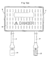
- a conventional terminal box B has a pair of terminal boards 2 arranged side by side in a top-open box body 1. Positive and negative electrodes a of a solar cell module M are connected to the respective terminal boards 2. A diode 3 for preventing countercurrent is mounted between the terminal boards 2 and cables P for outside connection are connected to the terminal boards 2 (see Patent publication 1).
- numeral 6 denotes a cover.
- Patent publication 1 JP patent publication 11-26035A
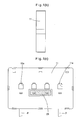
- Another terminal box B is known which is provided with three or more terminal boards 2 to connect a plurality of solar cell modules M for improved performance of the solar cell modules and higher current collecting efficiency (see Patent publication 2).
- a diode 3 for preventing countercurrent is provided between each adjacent pair of the terminal boards 2.
- Patent publication 2 JP patent publication 2002-359389A
- An object of the present invention is to prevent the temperature of the diode 3 from exceeding its junction temperature, with a simple and inexpensive means.
- a plurality of diodes are provided between each adjacent pair of the terminal boards in parallel to each other.
- the heat generated differs with different resistivities of diodes. Difference in the temperature of the diodes increases the difference in the resistivity, so that drift will increase. Therefore, the present invention aims to solve the problem by radiating heat of the diodes and making uniform the temperatures of the diodes arranged in parallel to each other.
- the reliability of diodes can be maintained without using expensive diodes having high heat resistance.
- the cost is reasonable and the construction is simple.
- drift can be prevented by providing drift prevention resistors, radiating heat from the diodes, or making uniform the temperatures of the diodes arranged in parallel to each other.
- One embodiment of this invention is a terminal box for solar cell modules comprising a box body, a plurality of terminal boards received in the box body for connection of electrodes a of the solar cell modules, and countercurrent prevention diodes 13 provided between adjacent ones of the terminal boards, characterized in that a plurality of the diodes are provided between each adjacent pair of the terminal boards in parallel to each other.
- a drift prevention resistor is connected in series with each diode to make uniform the loads borne by the diodes.
- the resistivity of the resistors are set properly based on the temperature rise of the diodes obtained by experiments for different manner of mounting.
- a temperature switch is preferably connected in series with each diode so that the switch will turn off to cut the current before each diode reaches its junction temperature, and turn on to supply the current to the diode when the temperature of the diode decreases. This prevents excessive temperature rise of the diodes.
- heat transfer plates may be mounted in continuous contact with the respective diodes to radiate heat from the diodes, thereby making uniform the temperatures of the diodes. Drift can be prevented by radiating heat from the diodes and making uniform the temperatures of the diodes.
- the heat transfer plates may be provided in any of the embodiments and may be provided integrally with the respective terminal boards.
- FIG. 1 Another embodiment of this invention is a terminal box for solar cell modules which comprises a box body, a plurality of terminal boards received in the box body for connection of electrodes of the solar cell modules, and countercurrent prevention diode provided between adjacent ones of the terminal boards, and each terminal board is provided with a heat radiating piece.
- a heat radiating piece By heat radiation through the heat radiating pieces, drift can be prevented.
- the manner of mounting of the heat radiating pieces may be determined by doing experiments so that its effect will be sufficient.
- the heat radiating pieces too, may be provided integrally with the terminal board.
- the heat transfer plates and the heat radiating pieces may be used. Part or whole of the heat radiating pieces (terminal boards) may serve as heat transfer plates. Both in such a combined embodiment and separate embodiments, the box body may be formed with heat radiating plates, heat radiating fins or heat radiating notches to restrict temperature rise of the diodes.
- a plurality of the countercurrent prevention diodes may be arranged between each adjacent pair of the terminal boards in a staggered fashion in the direction in which the terminal boards are arranged in parallel to each other. This arrangement further increases the heat radiating efficiency through the terminal boards and restricts the temperature rise of the diodes because pairs of the diodes as a heat source are staggered between the terminal boards, so that the heat sources are scattered.
- the diodes are located near the edges of the terminal boards to increase the degree of scattering.
- the countercurrent prevention diodes are preferably connected to the terminal boards by fitting leads of the diodes in notches of the terminal boards. If the diodes are fixed by soldering, they will suffer damage more or less and be liable to change in the resistivity. If they are fixed by fitting, soldering is not needed any more. So change in resistivity by soldering is avoided.
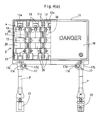
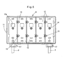
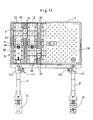
- Figs. 1(a) to 1(f) show one embodiment, which includes a rectangular box body 11 having an open top and made of polyphenylene oxide (PPO) resin or polyphenylene ether (PPE) resin and two pairs of terminal boards 12 (i.e. four terminal boards 12) arranged in parallel to each other.
- Positive and negative electrodes a of the solar cell modules M are connected to the respective terminal boards 12.
- Each of the electrodes a extends through a hole 11a and soldered to the center of one of the terminal boards 12.
- Spare solder 14 is provided at a point where each terminal board 12 is connected to the corresponding electrode a.
- a heat radiating sheet 15 made of a resin having high heat conductivity.
- the sheet 15 is formed with holes 15a through which the electrodes a are inserted for connection with the respective terminal boards.
- each cable P for outside connection is connected to the bottom (in Fig. 1a) of the box body 11 at both ends thereof.
- each cable P has its conductor connected to one of the the terminal boards 12 at both ends by pressing or welding, and is also fixed to the box body 11 by means of a cable lock 17 having a stopper ring 17a.
- a male connector 22 or female connector 21 which is connected to the female or male connector 21 or 22 of a cable P of the adjacent terminal box B.
- the front opening of the box body 11 is covered by a cover 16 of PPO or PPE resin, which is fitted through a waterproof ring (not shown) for watertightness.
- the box body 11 is filled with e.g. silicon resin, if necessary.
- the back of the box body 11 is subjected to creping and the terminal box B is fixed to the backs of the solar cell modules M through an adhesive tape 23 provided at its back.
- the terminal box B of this embodiment is bonded to the backs of the modules M keeping watertightness by use of seal material.
- Each cable P of the terminal box B are connected to female or male connector 21, 22 of a cable of the adjacent terminal box B.
- the terminal boxes B are thus connected in series or parallel by selecting the manner of connection.
- the diodes 13 it is possible to use ones having a junction temperature that is barely higher than the temperature determined by the amount of heat generated by each diode when a current i passes therethrough.
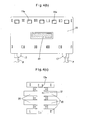
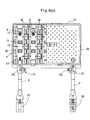
- Figs. 2 and 3 show other embodiments.
- a countercurrent prevention resistor 18 is connected in series with each diode 13 to make uniform the loads on the diodes 13.
- the resistivity of each resistor 18 is adjusted such that the current that flows through each diode 13 is substantially equal to the current that flows through any other diode (that is, the resistivity of each series circuit comprising one of the diodes 13 and one of the resistors 18 is substantially equal to the resistivity of any other series circuit).
- a temperature switch 19 such as a thermostat switch is connected in series with each diode 13 so that the switch 19 will turn off to cut the current before each diode 13 reaches its junction temperature, and turn on to supply the current to the diode when the temperature of the diode 13 decreases. This prevents excessive temperature rise of the diodes.
- each terminal board 12 is formed integrally with heat radiating pieces 20 protruding, as shown in Fig. 4(c), protruding from both side edges of the terminal board 12, which is in itself of a conventional structure.
- the terminal board 12 is fitted on the box body 11 with its heat radiating pieces 20 bent upward to increase its surface area and thus the heat radiating effect.
- the cable locks 17 each have an offset stopper 17c (shown in Fig.
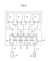
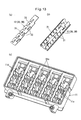
- the number of terminal boards 12 arranged in parallel to each other in each terminal box B is determined according to the number of solar cell modules M connected to the terminal box B. For example, three pairs of (i.e. six) terminal boards are arranged in each terminal box B if three modules M are connected to the terminal box B. But the number of terminal boards may be two, three, five (as shown in Fig. 5), or may be larger than six.
- the number of diodes 13 arranged in parallel to each other is also not limited to two, but may be three as shown in Fig. 4, four, five, or more. If an even number of terminal boards 12 are received in each terminal box, a pair of terminal boards 12 are provided for each module M.
- the terminal boards 12 are connected to the modules M e.g. as shown in Fig. 8.
- the terminal boards 12 each include the heat radiating pieces 20
- its shape is not particularly limited provided a sufficient heat radiating effect is achieved.
- heat radiating pieces 20 bent in a wavy fashion may be used.
- the terminal boards 12 take an upright position, so that the heat radiating effect increases. That is, the terminal boards 12 themselves serve as heat radiating pieces 20.
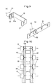
- heat transfer plate 30 may be provided each in contact with a plurality of diodes 13 to radiate heat from the diode 13. This makes uniform the temperatures of the diodes 13, thereby preventing drift.
- the heat transfer plates 30 may be made of any material that is high in heat conductivity. For example, they may be made of brass, and may be formed with as many notches 31 as the diodes 13 as shown in Figs. 9(a) and 9(b) to receive the leads 13a of the diodes 13.
- the heat transfer plates 30 shown in Fig. 9(a) may be mounted as shown in Fig. 1(d) by dotted lines, and those shown in Fig. 9(b) may be mounted as shown in Figs. 4(a), 6(a) and 6(c) by dotted lines.
- the diodes 13 may be brought into contact with the erected terminal boards 12. With this arrangement, because the terminal boards 12 serve as the heat transfer plates 30, the latter may be omitted.
- the plurality of countercurrent prevention diodes 13 arranged in parallel to each other between each adjacent pair of the terminal boards 12 may be disposed in a staggered fashion in the direction in which the terminal boards 12 are arranged in parallel to each other.
- This arrangement further increases the heat radiating efficiency through the terminal boards 12 and restricts the temperature rise of the diodes 13 because pairs of the diodes 13 as a heat source are staggered between the terminal boards 12, so that the heat sources are scattered.
- the pairs of the diodes 13 are located near the edges of the terminal boards 12 to increase the degree of scattering.
- Figs. 13(a) and 13(b) show other terminal boards 12 embodying the invention. These terminal boards 12 perform not only heat radiating function but heat transfer function according to the manner of mounting. They may be mounted in the terminal box B e.g. in the terminal boards 12 mounted in the box body 11 shown in Fig. 13(c) in the manner as shown in Fig. 12. With the arrangement shown in Fig. 12, the terminal boards 12 shown in Fig. 13(a) are mounted with their engaging pieces 32 in engagement with engaging pieces 11d of the box body 11. The terminal boards 12 shown in Fig. 13(b) are mounted with claws 11c of the box body 11 fitted in engaging holes 21 of the terminal boards 12. With this arrangement, each terminal board 12 will show heat radiating function of the heat radiating piece 20 and, if the body of the diodes 13 is in contact with the terminal boards 12, the latter will show the temperature uniforming function as the heat transfer plate 30.
- conductors 33 are mounted between the adjacent ones of the terminal boards 12 in their notches 31.
- the number of such conductors 33 is not limited.
- the box body 11 may be integrally or separately provided with heat radiating plates, fins or holes integrally to restrict temperature rise of the diodes 13.
- the diode 13 may have its leads 13a fitted in the notches 31 of the terminal boards 12. If this assures connection characteristics of the diode 13 to the terminal board 12, soldering is not necessary. This eliminates thermal stress during connection by soldering and prevents the performance of the diodes from decreasing due to thermal stress, thereby eliminating variation in the resistance value due to decrease in the performance.
- the diodes 13 with leads 13a are connected to the terminal boards 12 by soldering through the heat radiating pieces 20, their leads 13a are preferably soldered at points b as remote from the diode bodies as possible to minimize thermal stress in soldering. In this case, connection by soldering may be used together with connection by fitting in the notches 31.
Landscapes
- Physics & Mathematics (AREA)
- Condensed Matter Physics & Semiconductors (AREA)
- Electromagnetism (AREA)
- General Physics & Mathematics (AREA)
- Engineering & Computer Science (AREA)
- Computer Hardware Design (AREA)
- Microelectronics & Electronic Packaging (AREA)
- Power Engineering (AREA)
- Photovoltaic Devices (AREA)
Applications Claiming Priority (3)
| Application Number | Priority Date | Filing Date | Title |
|---|---|---|---|
| JP2004155105 | 2004-05-25 | ||
| JP2004374266 | 2004-12-24 | ||
| PCT/JP2005/009137 WO2005117141A1 (ja) | 2004-05-25 | 2005-05-19 | 太陽電池モジュール用端子ボックス |
Publications (2)
| Publication Number | Publication Date |
|---|---|
| EP1758176A1 true EP1758176A1 (de) | 2007-02-28 |
| EP1758176A4 EP1758176A4 (de) | 2007-08-01 |
Family
ID=35451163
Family Applications (1)
| Application Number | Title | Priority Date | Filing Date |
|---|---|---|---|
| EP05741410A Withdrawn EP1758176A4 (de) | 2004-05-25 | 2005-05-19 | Anschlussbox für ein solarzellenmodul |
Country Status (5)
| Country | Link |
|---|---|
| US (1) | US8330035B2 (de) |
| EP (1) | EP1758176A4 (de) |
| JP (1) | JP3965418B2 (de) |
| KR (1) | KR101040335B1 (de) |
| WO (1) | WO2005117141A1 (de) |
Cited By (9)
| Publication number | Priority date | Publication date | Assignee | Title |
|---|---|---|---|---|
| WO2008142016A1 (de) * | 2007-05-18 | 2008-11-27 | Anton Gensler Gmbh | Elektrische anschlusseinrichtung für photovoltaische module |
| WO2009021647A1 (en) * | 2007-08-10 | 2009-02-19 | Tyco Electronics Amp Gmbh | Electrical connection system for photovoltaic solar installations |
| WO2009076917A1 (de) * | 2007-12-15 | 2009-06-25 | Lumberg Connect Gmbh | Steckverbinder für photovoltaikkabelsätze |
| FR2928784A1 (fr) * | 2008-03-14 | 2009-09-18 | Bertrand Courtaigne | Dispositif de raccordement electrique notamment pour panneau solaire electrique |
| CN101272039B (zh) * | 2007-03-23 | 2010-04-14 | 励国庆 | 快速接线盒 |
| FR2949615A1 (fr) * | 2009-08-28 | 2011-03-04 | Bertrand Courtaigne | Dispositif de raccordement electrique particulierement adapte aux panneaux solaires electriques ou a d'autres producteurs d'energie |
| WO2010079142A3 (de) * | 2009-01-08 | 2011-09-22 | Yamaichi Electronics Deutschland Gmbh | Solarpaneel und verfahren |
| DE112006002980B4 (de) * | 2005-11-09 | 2013-11-14 | Sumitomo Wiring Systems, Ltd. | Anschlußkasten für Solarzellenmodul |
| EP2423978A3 (de) * | 2010-08-30 | 2013-12-04 | Hosiden Corporation | Verteilerkasten |
Families Citing this family (44)
| Publication number | Priority date | Publication date | Assignee | Title |
|---|---|---|---|---|
| JP5078388B2 (ja) * | 2006-04-27 | 2012-11-21 | 京セラ株式会社 | 太陽電池モジュールおよび太陽電池モジュールの製造方法 |
| CN102891200A (zh) * | 2006-06-29 | 2013-01-23 | 胡贝尔和茹纳股份公司 | 接线盒 |
| FR2907266B1 (fr) * | 2006-10-13 | 2008-12-12 | Bertrand Courtaigne | Dispositif de raccordement electrique notamment pour panneau solaire electrique |
| CN101647123B (zh) * | 2007-04-13 | 2012-08-29 | 胡贝尔和茹纳股份公司 | 连接盒 |
| JP4167715B1 (ja) * | 2007-08-13 | 2008-10-22 | オーナンバ株式会社 | ツインチップ搭載型ダイオード |
| US20100186821A1 (en) * | 2007-10-01 | 2010-07-29 | Suinno Oy | Thermodynamically shielded solar cell |
| DE102008022297B4 (de) * | 2008-03-13 | 2011-04-14 | Fpe Fischer Gmbh | Verbindungsbox für Solar-Module und Verfahren zu deren Montage an den Modulen |
| WO2009129405A2 (en) * | 2008-04-16 | 2009-10-22 | Molex Incorporated | Solar panel junction box |
| DE102008022051A1 (de) * | 2008-05-03 | 2009-11-19 | Lumberg Connect Gmbh | Anschlussdose für ein Solarmodul |
| EP2360210B1 (de) * | 2008-10-24 | 2015-12-23 | Asahi Kasei Chemicals Corporation | Verbindungsstruktur für ein Modul zur photovoltaischen Stromerzeugung |
| DE102008062034B4 (de) * | 2008-12-12 | 2010-08-12 | Tyco Electronics Amp Gmbh | Verbindungsvorrichtung zum Anschluss an ein Solarmodul und Solarmodul mit einer solchen Verbindungsvorrichtung |
| US7862383B2 (en) * | 2009-06-03 | 2011-01-04 | Tyco Electronics Corporation | Electrical connector for a solar module assembly |
| EP2450962B1 (de) * | 2009-06-29 | 2019-02-13 | Kyocera Corporation | Verteilerkasten für solarzellenmodule und solarzellenmodul damit |
| DE102010002565B8 (de) * | 2010-03-04 | 2012-03-22 | Tyco Electronics Amp Gmbh | Anschlussvorrichtung für ein Solarmodul |
| US20130003307A1 (en) * | 2010-03-11 | 2013-01-03 | Hyung Suk Jang | Solar cell module junction box |
| KR101012003B1 (ko) * | 2010-08-13 | 2011-01-31 | 동진에스앤씨 주식회사 | 태양광 발전모듈용 정션박스 |
| CN102386257A (zh) * | 2010-08-30 | 2012-03-21 | 杜邦太阳能有限公司 | 光伏模块及其接线盒 |
| TWI423496B (zh) * | 2010-10-20 | 2014-01-11 | Energy Control Ltd | 以複數個電池模組疊設構成具散熱構造的集合電池 |
| JPWO2012111628A1 (ja) | 2011-02-14 | 2014-07-07 | 旭化成ケミカルズ株式会社 | 太陽光発電モジュール用接続構造体 |
| US8519278B2 (en) * | 2011-02-16 | 2013-08-27 | Amphenol Corporation | Photovoltaic junction box |
| KR101228041B1 (ko) * | 2011-03-14 | 2013-02-19 | 동아전장주식회사 | 정션박스 |
| JP5594902B2 (ja) * | 2011-04-18 | 2014-09-24 | モレックス インコーポレイテド | 太陽電池パネル用コネクタ及び太陽電池パネル連結体 |
| CN202111117U (zh) * | 2011-05-05 | 2012-01-11 | 泰科电子(上海)有限公司 | 太阳能电池板接线模块 |
| JP5978421B2 (ja) | 2011-06-20 | 2016-08-24 | 旭化成株式会社 | ポリフェニレンエーテル系樹脂組成物及びその製造方法 |
| JP5612543B2 (ja) * | 2011-06-22 | 2014-10-22 | ホシデン株式会社 | 太陽電池モジュールの端子構造 |
| JP2013055304A (ja) * | 2011-09-06 | 2013-03-21 | Nippon Tanshi Kk | 端子ボックス用端子部材 |
| JP5729648B2 (ja) * | 2011-10-13 | 2015-06-03 | ホシデン株式会社 | 太陽電池モジュール用端子ボックス |
| KR101141288B1 (ko) | 2011-11-24 | 2012-05-04 | (주) 대하전선 | 태양광모듈의 단자박스 |
| KR101138991B1 (ko) | 2011-11-24 | 2012-04-25 | (주) 대하전선 | 태양광모듈 단자박스의 단자 설치 구조 |
| KR101138990B1 (ko) | 2011-11-24 | 2012-04-25 | (주) 대하전선 | 태양광 모듈의 단자 박스 |
| KR101138993B1 (ko) | 2011-11-24 | 2012-04-25 | (주) 대하전선 | 태양광 모듈의 단자 박스 방수구조 |
| KR101138995B1 (ko) | 2011-11-24 | 2012-04-25 | (주) 대하전선 | 태양광모듈 단자박스의 방열구조 |
| US9635783B2 (en) * | 2012-03-30 | 2017-04-25 | Sunpower Corporation | Electronic component housing with heat sink |
| KR200468714Y1 (ko) * | 2012-04-10 | 2013-09-02 | 한맥전자 (주) | 내부 발열 방지용 정션박스 |
| JP5777580B2 (ja) * | 2012-08-06 | 2015-09-09 | 三菱電機株式会社 | 端子ボックス |
| JP6058124B2 (ja) * | 2013-04-02 | 2017-01-11 | 三菱電機株式会社 | 端子ボックス及び太陽電池モジュール |
| JP6094015B2 (ja) * | 2013-04-12 | 2017-03-15 | ホシデン株式会社 | 端子ボックス |
| KR101440351B1 (ko) * | 2014-02-03 | 2014-09-18 | (주) 대하전선 | 태양광 모듈의 단자 박스 커버 |
| US9445515B2 (en) * | 2014-02-20 | 2016-09-13 | Tyco Electronics Corporation | Circuit box |
| JP6558013B2 (ja) * | 2015-03-24 | 2019-08-14 | 住友電気工業株式会社 | フレキシブルプリント配線板の接合構造、集光型太陽光発電モジュール、及び、フレキシブルプリント配線板の接合方法 |
| KR101666147B1 (ko) * | 2016-02-03 | 2016-10-13 | 운지파워텍(주) | 태양광발전시스템의 접속반 방열장치 |
| JP2019092234A (ja) * | 2016-03-25 | 2019-06-13 | パナソニックIpマネジメント株式会社 | 端子ボックス |
| EP4318938A3 (de) | 2017-03-29 | 2024-05-01 | Solaredge Technologies Ltd. | Wärmeableitung für einen fotovoltaischen anschlusskasten |
| KR102397979B1 (ko) * | 2017-05-31 | 2022-05-13 | 엘지전자 주식회사 | 태양 전지 모듈 |
Citations (5)
| Publication number | Priority date | Publication date | Assignee | Title |
|---|---|---|---|---|
| WO2000030216A1 (en) * | 1998-11-17 | 2000-05-25 | Utilux Pty. Limited | Solar panel cable connector |
| JP2000261177A (ja) * | 1999-03-05 | 2000-09-22 | Nitto Electric Works Ltd | 太陽光発電システム用集電ボックス |
| JP2001168368A (ja) * | 1999-12-09 | 2001-06-22 | Kanegafuchi Chem Ind Co Ltd | 端子ボックス |
| US20030193322A1 (en) * | 2002-04-10 | 2003-10-16 | Sumitomo Wiring Systems, Ltd. | Terminal box apparatus for solar cell module |
| US20040047118A1 (en) * | 2001-11-07 | 2004-03-11 | Eduard Bergmann | Assembly comprised of a panel-like constructed module and of a connection unit, production method and device |
Family Cites Families (24)
| Publication number | Priority date | Publication date | Assignee | Title |
|---|---|---|---|---|
| JPS5853164A (ja) | 1981-09-24 | 1983-03-29 | Toshiba Corp | 燃料電池装置 |
| JPS5853164U (ja) * | 1981-10-07 | 1983-04-11 | 株式会社東芝 | 半導体整流器 |
| JP2550618B2 (ja) | 1987-11-12 | 1996-11-06 | 富士通株式会社 | ページ捲り機構 |
| JPH01127391U (de) * | 1988-02-23 | 1989-08-31 | ||
| JP2544264Y2 (ja) * | 1991-06-21 | 1997-08-13 | 三洋電機株式会社 | 太陽電池パネル用端子ボックス |
| JPH051253A (ja) | 1991-06-24 | 1993-01-08 | Taniguchi Ink Seizo Kk | 印刷インキ |
| JPH06314760A (ja) | 1993-04-28 | 1994-11-08 | Isuzu Motors Ltd | 半導体素子の実装機構 |
| JP3412194B2 (ja) | 1993-07-09 | 2003-06-03 | 三菱電機株式会社 | 内燃機関用点火装置 |
| JPH0732994A (ja) | 1993-07-20 | 1995-02-03 | Tokico Ltd | 液圧制御弁 |
| JP3439891B2 (ja) | 1995-10-31 | 2003-08-25 | 京セラ株式会社 | 太陽光発電装置 |
| JP3069523B2 (ja) | 1996-05-27 | 2000-07-24 | 西部電機株式会社 | 洗浄装置付きパレット取扱装置 |
| JPH1126035A (ja) | 1997-07-04 | 1999-01-29 | Engel Kogyo Kk | 太陽電池モジュール用端子ボックス |
| JPH11195889A (ja) | 1997-12-27 | 1999-07-21 | Nec Home Electron Ltd | プリント基板用放熱部品 |
| JP3656391B2 (ja) * | 1998-03-02 | 2005-06-08 | 三菱電機株式会社 | 太陽電池モジュール |
| JPH11330521A (ja) * | 1998-03-13 | 1999-11-30 | Canon Inc | 太陽電池モジュ―ル、太陽電池アレイ、太陽光発電装置、太陽電池モジュ―ルの故障特定方法 |
| JP3601293B2 (ja) * | 1998-04-16 | 2004-12-15 | 三菱電機株式会社 | 太陽電池モジュール |
| DE19916742C1 (de) * | 1999-04-13 | 2000-08-24 | Angew Solarenergie Ase Gmbh | Schaltungsanordnung zur Stromerzeugung mit Solarzellen |
| JP2001024371A (ja) | 1999-07-06 | 2001-01-26 | Kenwood Corp | プリント基板の放熱装置 |
| JP2001135847A (ja) * | 1999-11-05 | 2001-05-18 | Kanegafuchi Chem Ind Co Ltd | 半導体装置及びこれを備えた端子ボックス |
| JP2001168363A (ja) * | 1999-12-10 | 2001-06-22 | Toyota Central Res & Dev Lab Inc | 太陽電池の製造方法 |
| JP4004203B2 (ja) * | 2000-03-03 | 2007-11-07 | 三洋電機株式会社 | 太陽電池モジュール |
| JP2002359389A (ja) | 2001-05-31 | 2002-12-13 | Kitani Denki Kk | 太陽光発電モジュール配線用端子ボックス |
| JP2003347490A (ja) | 2002-05-30 | 2003-12-05 | Mitsumi Electric Co Ltd | 電子部品の放熱装置 |
| JP2004221210A (ja) * | 2003-01-14 | 2004-08-05 | Kyocera Corp | 太陽電池モジュール |
-
2005
- 2005-05-19 WO PCT/JP2005/009137 patent/WO2005117141A1/ja active Application Filing
- 2005-05-19 JP JP2006513857A patent/JP3965418B2/ja active Active
- 2005-05-19 KR KR1020067023901A patent/KR101040335B1/ko active IP Right Grant
- 2005-05-19 EP EP05741410A patent/EP1758176A4/de not_active Withdrawn
- 2005-05-19 US US11/597,421 patent/US8330035B2/en active Active
Patent Citations (5)
| Publication number | Priority date | Publication date | Assignee | Title |
|---|---|---|---|---|
| WO2000030216A1 (en) * | 1998-11-17 | 2000-05-25 | Utilux Pty. Limited | Solar panel cable connector |
| JP2000261177A (ja) * | 1999-03-05 | 2000-09-22 | Nitto Electric Works Ltd | 太陽光発電システム用集電ボックス |
| JP2001168368A (ja) * | 1999-12-09 | 2001-06-22 | Kanegafuchi Chem Ind Co Ltd | 端子ボックス |
| US20040047118A1 (en) * | 2001-11-07 | 2004-03-11 | Eduard Bergmann | Assembly comprised of a panel-like constructed module and of a connection unit, production method and device |
| US20030193322A1 (en) * | 2002-04-10 | 2003-10-16 | Sumitomo Wiring Systems, Ltd. | Terminal box apparatus for solar cell module |
Non-Patent Citations (1)
| Title |
|---|
| See also references of WO2005117141A1 * |
Cited By (12)
| Publication number | Priority date | Publication date | Assignee | Title |
|---|---|---|---|---|
| DE112006002980B4 (de) * | 2005-11-09 | 2013-11-14 | Sumitomo Wiring Systems, Ltd. | Anschlußkasten für Solarzellenmodul |
| CN101272039B (zh) * | 2007-03-23 | 2010-04-14 | 励国庆 | 快速接线盒 |
| EP1973210A3 (de) * | 2007-03-23 | 2011-05-18 | Guoqing, Li | Verteilerkasten |
| WO2008142016A1 (de) * | 2007-05-18 | 2008-11-27 | Anton Gensler Gmbh | Elektrische anschlusseinrichtung für photovoltaische module |
| WO2009021647A1 (en) * | 2007-08-10 | 2009-02-19 | Tyco Electronics Amp Gmbh | Electrical connection system for photovoltaic solar installations |
| WO2009076917A1 (de) * | 2007-12-15 | 2009-06-25 | Lumberg Connect Gmbh | Steckverbinder für photovoltaikkabelsätze |
| FR2928784A1 (fr) * | 2008-03-14 | 2009-09-18 | Bertrand Courtaigne | Dispositif de raccordement electrique notamment pour panneau solaire electrique |
| WO2010079142A3 (de) * | 2009-01-08 | 2011-09-22 | Yamaichi Electronics Deutschland Gmbh | Solarpaneel und verfahren |
| FR2949615A1 (fr) * | 2009-08-28 | 2011-03-04 | Bertrand Courtaigne | Dispositif de raccordement electrique particulierement adapte aux panneaux solaires electriques ou a d'autres producteurs d'energie |
| EP2423978A3 (de) * | 2010-08-30 | 2013-12-04 | Hosiden Corporation | Verteilerkasten |
| US8723031B2 (en) | 2010-08-30 | 2014-05-13 | Hosiden Corporation | Terminal box |
| US8866013B2 (en) | 2010-08-30 | 2014-10-21 | Hosiden Corporation | Terminal box |
Also Published As
| Publication number | Publication date |
|---|---|
| US8330035B2 (en) | 2012-12-11 |
| WO2005117141A1 (ja) | 2005-12-08 |
| KR20070029171A (ko) | 2007-03-13 |
| EP1758176A4 (de) | 2007-08-01 |
| US20080190477A1 (en) | 2008-08-14 |
| JPWO2005117141A1 (ja) | 2008-04-03 |
| JP3965418B2 (ja) | 2007-08-29 |
| KR101040335B1 (ko) | 2011-06-10 |
Similar Documents
| Publication | Publication Date | Title |
|---|---|---|
| US8330035B2 (en) | Terminal box for solar cell modules | |
| JP6656373B2 (ja) | 電池モジュール内に占める空間が少ない相互連結部材及びこれを備える電池モジュール | |
| US8197263B2 (en) | Electric connection receptable for a solar cell module | |
| US7291036B1 (en) | Photovoltaic connection system | |
| US20080115822A1 (en) | Cable Connectors for a Photovoltaic Module and Method of Installing | |
| US20090084570A1 (en) | Low Profile Photovoltaic (LPPV) Box | |
| US8519278B2 (en) | Photovoltaic junction box | |
| WO2007052407A1 (ja) | 太陽電池モジュール用端子ボックス | |
| WO2008060509A2 (en) | Junction box for solar cells with bypass diodes and heat sink | |
| US20080253092A1 (en) | Heat Dissipation System for Photovoltaic Interconnection System | |
| US10972046B2 (en) | Circuits and methods for controlling current in a parallel-connected array | |
| EP3314746B1 (de) | Klemme für eine solaranschlussdose | |
| JP4129037B2 (ja) | 太陽電池モジュール用端子ボックス | |
| CN100521251C (zh) | 太阳能电池组件用端子盒 | |
| JP2005150277A (ja) | 太陽電池モジュール用端子ボックス | |
| JP5144201B2 (ja) | 太陽電池モジュール用端子ボックス | |
| JP2007189256A (ja) | 太陽電池モジュール用端子ボックス | |
| JP4046756B2 (ja) | 太陽電池モジュール用端子ボックス | |
| JP2004289181A (ja) | 太陽電池モジュール用接続箱 | |
| CN216216757U (zh) | 分体式接线装置 | |
| CN217656182U (zh) | 汇流条组件 | |
| CN216721272U (zh) | 简易型光伏接线盒及光伏组件 | |
| JP5969369B2 (ja) | 導体積層体、太陽光発電システム用接続箱、及び太陽光発電システム | |
| CN221081269U (en) | Photovoltaic inverter | |
| JP5523227B2 (ja) | 太陽電池モジュール用端子ボックス |
Legal Events
| Date | Code | Title | Description |
|---|---|---|---|
| PUAI | Public reference made under article 153(3) epc to a published international application that has entered the european phase |
Free format text: ORIGINAL CODE: 0009012 |
|
| 17P | Request for examination filed |
Effective date: 20061128 |
|
| AK | Designated contracting states |
Kind code of ref document: A1 Designated state(s): DE ES GR |
|
| A4 | Supplementary search report drawn up and despatched |
Effective date: 20070704 |
|
| DAX | Request for extension of the european patent (deleted) | ||
| RBV | Designated contracting states (corrected) |
Designated state(s): DE ES GR |
|
| 17Q | First examination report despatched |
Effective date: 20150910 |
|
| GRAP | Despatch of communication of intention to grant a patent |
Free format text: ORIGINAL CODE: EPIDOSNIGR1 |
|
| RIC1 | Information provided on ipc code assigned before grant |
Ipc: H01L 31/042 20140101AFI20170920BHEP Ipc: H05K 7/20 20060101ALI20170920BHEP Ipc: H01L 25/11 20060101ALI20170920BHEP Ipc: H01R 9/28 20060101ALI20170920BHEP Ipc: H02S 40/34 20140101ALI20170920BHEP |
|
| INTG | Intention to grant announced |
Effective date: 20171026 |
|
| RIN1 | Information on inventor provided before grant (corrected) |
Inventor name: HATTORI, YUTAKA |
|
| STAA | Information on the status of an ep patent application or granted ep patent |
Free format text: STATUS: THE APPLICATION IS DEEMED TO BE WITHDRAWN |
|
| 18D | Application deemed to be withdrawn |
Effective date: 20180306 |