EP1756860B1 - Method of semiconductor fabrication in corporating disposable spacer into elevated source/drain processing - Google Patents
Method of semiconductor fabrication in corporating disposable spacer into elevated source/drain processing Download PDFInfo
- Publication number
- EP1756860B1 EP1756860B1 EP05735763A EP05735763A EP1756860B1 EP 1756860 B1 EP1756860 B1 EP 1756860B1 EP 05735763 A EP05735763 A EP 05735763A EP 05735763 A EP05735763 A EP 05735763A EP 1756860 B1 EP1756860 B1 EP 1756860B1
- Authority
- EP
- European Patent Office
- Prior art keywords
- spacer
- drain
- gate electrode
- silicon nitride
- forming
- Prior art date
- Legal status (The legal status is an assumption and is not a legal conclusion. Google has not performed a legal analysis and makes no representation as to the accuracy of the status listed.)
- Expired - Lifetime
Links
Images


Classifications
-
- H—ELECTRICITY
- H10—SEMICONDUCTOR DEVICES; ELECTRIC SOLID-STATE DEVICES NOT OTHERWISE PROVIDED FOR
- H10D—INORGANIC ELECTRIC SEMICONDUCTOR DEVICES
- H10D30/00—Field-effect transistors [FET]
- H10D30/01—Manufacture or treatment
- H10D30/021—Manufacture or treatment of FETs having insulated gates [IGFET]
- H10D30/027—Manufacture or treatment of FETs having insulated gates [IGFET] of lateral single-gate IGFETs
- H10D30/0275—Manufacture or treatment of FETs having insulated gates [IGFET] of lateral single-gate IGFETs forming single crystalline semiconductor source or drain regions resulting in recessed gates, e.g. forming raised source or drain regions
-
- H—ELECTRICITY
- H10—SEMICONDUCTOR DEVICES; ELECTRIC SOLID-STATE DEVICES NOT OTHERWISE PROVIDED FOR
- H10D—INORGANIC ELECTRIC SEMICONDUCTOR DEVICES
- H10D30/00—Field-effect transistors [FET]
- H10D30/01—Manufacture or treatment
- H10D30/021—Manufacture or treatment of FETs having insulated gates [IGFET]
- H10D30/0212—Manufacture or treatment of FETs having insulated gates [IGFET] using self-aligned silicidation
-
- H—ELECTRICITY
- H10—SEMICONDUCTOR DEVICES; ELECTRIC SOLID-STATE DEVICES NOT OTHERWISE PROVIDED FOR
- H10D—INORGANIC ELECTRIC SEMICONDUCTOR DEVICES
- H10D30/00—Field-effect transistors [FET]
- H10D30/01—Manufacture or treatment
- H10D30/021—Manufacture or treatment of FETs having insulated gates [IGFET]
- H10D30/022—Manufacture or treatment of FETs having insulated gates [IGFET] having lightly-doped source or drain extensions selectively formed at the sides of the gates
-
- H—ELECTRICITY
- H10—SEMICONDUCTOR DEVICES; ELECTRIC SOLID-STATE DEVICES NOT OTHERWISE PROVIDED FOR
- H10D—INORGANIC ELECTRIC SEMICONDUCTOR DEVICES
- H10D30/00—Field-effect transistors [FET]
- H10D30/01—Manufacture or treatment
- H10D30/021—Manufacture or treatment of FETs having insulated gates [IGFET]
- H10D30/031—Manufacture or treatment of FETs having insulated gates [IGFET] of thin-film transistors [TFT]
- H10D30/0321—Manufacture or treatment of FETs having insulated gates [IGFET] of thin-film transistors [TFT] comprising silicon, e.g. amorphous silicon or polysilicon
- H10D30/0323—Manufacture or treatment of FETs having insulated gates [IGFET] of thin-film transistors [TFT] comprising silicon, e.g. amorphous silicon or polysilicon comprising monocrystalline silicon
-
- H—ELECTRICITY
- H10—SEMICONDUCTOR DEVICES; ELECTRIC SOLID-STATE DEVICES NOT OTHERWISE PROVIDED FOR
- H10D—INORGANIC ELECTRIC SEMICONDUCTOR DEVICES
- H10D30/00—Field-effect transistors [FET]
- H10D30/60—Insulated-gate field-effect transistors [IGFET]
- H10D30/601—Insulated-gate field-effect transistors [IGFET] having lightly-doped drain or source extensions, e.g. LDD IGFETs or DDD IGFETs
- H10D30/608—Insulated-gate field-effect transistors [IGFET] having lightly-doped drain or source extensions, e.g. LDD IGFETs or DDD IGFETs having non-planar bodies, e.g. having recessed gate electrodes
-
- H—ELECTRICITY
- H10—SEMICONDUCTOR DEVICES; ELECTRIC SOLID-STATE DEVICES NOT OTHERWISE PROVIDED FOR
- H10D—INORGANIC ELECTRIC SEMICONDUCTOR DEVICES
- H10D64/00—Electrodes of devices having potential barriers
- H10D64/01—Manufacture or treatment
- H10D64/015—Manufacture or treatment removing at least parts of gate spacers, e.g. disposable spacers
-
- H—ELECTRICITY
- H10—SEMICONDUCTOR DEVICES; ELECTRIC SOLID-STATE DEVICES NOT OTHERWISE PROVIDED FOR
- H10D—INORGANIC ELECTRIC SEMICONDUCTOR DEVICES
- H10D64/00—Electrodes of devices having potential barriers
- H10D64/01—Manufacture or treatment
- H10D64/021—Manufacture or treatment using multiple gate spacer layers, e.g. bilayered sidewall spacers
-
- H—ELECTRICITY
- H10—SEMICONDUCTOR DEVICES; ELECTRIC SOLID-STATE DEVICES NOT OTHERWISE PROVIDED FOR
- H10P—GENERIC PROCESSES OR APPARATUS FOR THE MANUFACTURE OR TREATMENT OF DEVICES COVERED BY CLASS H10
- H10P30/00—Ion implantation into wafers, substrates or parts of devices
- H10P30/20—Ion implantation into wafers, substrates or parts of devices into semiconductor materials, e.g. for doping
- H10P30/222—Ion implantation into wafers, substrates or parts of devices into semiconductor materials, e.g. for doping characterised by the angle between the ion beam and the crystal planes or the main crystal surface
Definitions
- the invention is in the filed of semiconductor fabrication and more specifically in semiconductor fabrication processes employing elevated source/drain processing.
- SOI wafers incorporate a shallow silicon region (in which transistor structures such as the transistor channel are located) overlying a buried, electrically insulating layer such as silicon dioxide.
- the shallow silicon layer may be too shallow to contain the transistor source/drain regions without exhibiting undesirable and performance limiting current crowding. Elevated source/drain structures alleviate this problem by providing a thicker silicon film where the source/drain regions are formed.
- elevated source/drain structures are fabricated with a selective epitaxial process.
- the epitaxial process that forms the elevated source/drain regions introduces an additional thermal cycle into the processing sequence.
- the additional thermal cycle has an undesirable impact on impurity distributions that have already been introduced into the wafer.
- these impurity distributions may include the halo and extension impurity distributions that are well known in the filed of CMOS fabrication. Because it is generally highly desirable to minimize the depth of the halo and extension implant distributions, the additional thermal cycle represented by the epitaxial process is problematic.
- the present invention relates to a semiconductor fabrication process in which a disposable spacer is used in conjunction with elevated source/drain processing to provide a reliable elevated source/drain process sequence.
- a disposable spacer is used in conjunction with elevated source/drain processing to provide a reliable elevated source/drain process sequence.
- the use of an offset spacer in conjunction with a disposable spacer beneficially prevents the formation of unwanted structures, such as "mouse ears" on the gate electrode, during the elevated source/drain formation sequence while still enabling the introduction of shallow implants after the elevated source/drain formation.
- a silicon nitride offset spacer is used to prevent formation of so-called “mouse ears" at the corners of the transistor gate electrode during epitaxial processing of the elevated source/drain.
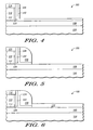
- a wafer 100 is depicted at a first selected stage of a fabrication process according to the present invention.
- wafer 100 is a silicon-on-insulator (SOI) wafer that includes a silicon layer 108 overlying a buried oxide (BOX) layer 104.
- BOX layer 104 is likely overlying a silicon bulk region (not depicted) of wafer 100.
- Silicon layer 108 is preferably single crystal silicon having a thickness of approximately 700 Angstroms and BOX layer 104 is preferably a silicon oxide compound such as silicon dioxide having a thickness of approximately 1400 Angstroms.
- wafer 100 includes a gate structure overlying silicon layer 108.
- the gate structure includes a gate dielectric 112 overlying silicon layer 108, a conductive gate electrode 110 overlying gate dielectric 112, and a capping layer 114 overlying gate electrode 110.
- gate dielectric 112 is a silicon oxide compound such as thermally formed silicon dioxide and gate electrode 110 is a conventional polysilicon gate electrode.
- gate dielectric 112 may include a "high-K" dielectric material (i.e., a dielectric having a dielectric constant greater than the dielectric constant of silicon dioxide) such as hafnium oxide (HfO) while gate electrode 110 may include one or more metal materials such as titanium, tantalum, and alloys thereof.
- Capping layer 114 preferably provides an antireflective coating (ARC) over gate electrode 110.
- ARC antireflective coating
- capping layer 114 is a silicon nitride film.
- the elevated source/drain processing is initiated by forming an oxide dielectric liner 120 on the exterior of gate electrode 110 and the upper surface of silicon layer 108.
- the liner 120 is a relatively thin silicon oxide liner of approximately 23 Angstroms formed by thermally oxidizing polysilicon gate electrode 110 (and silicon layer 108).
- offset spacer 122 is formed on the sidewall of liner dielectric 120 adjacent the sidewalls of gate electrode 110.
- offset spacer 122 is formed by depositing silicon nitride on wafer 100 using a CVD reactor and thereafter anisotropically etching the deposited film to leave silicon nitride on vertically oriented surfaces such as the sidewalls of liner dielectric 120 while removing the silicon nitride from horizontally oriented surfaces such as the upper surface of liner dielectric 120 over silicon layer 108.
- offset spacer 122 contacts ARC 114 and thereby beneficially encloses or surrounds gate electrode 110 in silicon nitride to provide a protective barrier for the gate electrode during subsequent processing and, more specifically, during subsequent silicon formation processing.
- a 15nm (150 Angstrom) thick layer of silicon nitride is deposited and etch to form offset spacer 122.
- an intermediate liner dielectric of silicon oxide 124 is formed on the sidewalls of offset spacer 122 and the upper surface of liner dielectric 120.
- intermediate liner dielectric 124 is a CVD silicon-oxide film preferably having a thickness of approximately 150 Angstroms.
- first liner dielectric 120 is a thermally formed oxide
- second liner dielectric is a CVD oxide
- the etch rate of first liner dielectric 120 in HF solution is significantly less than the etch rate of second dielectric 124.
- the slower etch rate of liner dielectric 120 will ensure that liner dielectric 120 beneficially remains intact during subsequent processing to protect the gate electrode and provide mechanical support for the offset spacer 122.
- disposable spacer 130 a spacer of silicon nitride, referred to herein as disposable spacer 130, has been formed on the sidewalls of intermediate liner dielectric 124 adjacent the offset spacer 122.
- disposable spacer is formed by depositing approximately (900 Angstroms) of silicon nitride followed by an anisotropic silicon nitride etch.
- Disposable 90nm spacer 130 may then be subjected to a rapid thermal anneal (e.g., 5 seconds at 1060 °C) to "densify" the as-deposited silicon nitride.
- Disposable spacer 130 (in conjunction with capping layer 114 and offset spacer 122) serves as a mask that defines the portions of the underlying silicon wafer 108 on which an elevated source/drain structure will be formed.
- silicon wafer 100 beneficially incorporates disposable spacer 130 that enables the formation of elevated source/drain regions prior to shallow implant processes, such as extension and halo implant processes, that would be negatively impacted by the high temperature process required to form the elevated source/drain epitaxially.
- the inclusion of the offset spacer 122 and ARC 114 protects gate electrode 110 during the high temperature silicon formation process thereby preventing the formation of so-called mouse ears at the corners of the gate electrode.
- wafer 100 as depicted in FIG. 5 is suitable for be subjected to an epitaxial or other high temperature, silicon formation process, such as an elevated source/drain formation process sequence, without jeopardizing the physical dimensions of the gate electrode structure.
- the presently described invention promotes superior repeatability and reliability by providing better protection of the gate electrode.
- the gate electrode 110 of the present invention is sealed within a silicon nitride enclosure formed when offset spacer 122 is formed in contact with ARC 114.
- offset spacer 122 provides a good etch stop during subsequent etch processing and a desirable offset spacer for shallow implants.
- an elevated silicon layer 132 is formed overlying the exposed portions of silicon layer 108 (i.e., the portions of silicon layer 108 covered by neither gate electrode 110 nor disposable spacer 130).
- the preferred embodiment of forming elevated source/drain layer 132 includes epitaxial growth of elevated source/drain layer 132 using a silicon-chloride source such as SiHCL 3 at a temperature in excess of 1000 °C.
- a thickness of elevated source/drain layer 132 in one implementation is in the range of approximately 200 to 300 Angstroms. The presence of disposable spacer 130 during the epitaxial processing prevents formation of the epitaxial layer below the spacer.
- offset spacer 122 and ARC 114 prevent the epitaxial processing from affecting the profile of gate electrode 110.
- a thin (i.e., less than 2,5nm (25 Angstroms)) layer of oxide is thermally grown overlying elevated source/drain 132. This thin oxide, which is subsequently stripped, is a sacrificial layer that consumes contaminants and imperfections at the upper surface of the epitaxial film.
- disposable spacer 130 and intermediate liner dielectric 124 are removed without removing offset spacer 122 to expose portions of silicon layer 108 in close proximity to gate electrode 110 (displaced laterally from gate electrode 110 only by the combined thickness of liner 120 and offset spacer 122).
- Disposable spacer 130 is preferably removed by dipping wafer 100 in a phosphoric acid solution heated to 1 80 °C while second liner dielectric 124 is removed with an HF dip or another suitable etching process. If the HF is properly controlled, the thermally formed first liner dielectric 120 underlying offset spacer 122 will remain intact after CVD second liner dielectric 124 is removed due to differences in their respective etch rates in HF.
- the oxide-nitride-oxide-nitride layering of liner 120, spacer 122, liner 124, and spacer 130 enables the separate removal of each film thereby facilitating the removal of disposable spacer 130 without affecting offset spacer 122.
- the presence of offset spacer 122 beneficially protects the sidewalls of gate electrode 110 during removal of second liner dielectric 124.
- the removal of disposable spacer 130 also removes ARC 114 (as seen in FIG. 7 ).
- the removal of spacer 130 and liner 124 exposes the upper surface of silicon layer 108 proximal to gate electrode 110.
- Halo implant 140 is a angled implant that introduces an impurity of the same species as the well region in which it is introduced.
- Extension implant 142 introduces an opposite type impurity into each well region.
- Halo implant 140 is a P-type dopant such as boron while extension implant 142 is an N-type dopant such as phosphorous or arsenic.
- offset spacer 122 which has a thickness of approximately 100 Angstroms during the shallow implants is beneficial in optimizing the location of the implanted impurity distributions relative to gate electrode 110 and the underlying transistor channel.
- a third liner dielectric 134 and a replacement spacer 136 are formed where disposable spacer 130 and liner 124 existed previously to cover the portion of silicon layer 108 exposed when the disposable spacer was removed.
- the formation of liner 134 and spacer 136 is substantially equivalent to the formation of second liner dielectric 124 and disposable spacer 130.
- third liner dielectric 134 is a silicon oxide layer while replacement spacer 136 is silicon nitride.
- a source/drain implant represented by reference numeral 140 is performed to introduce a source/drain impurity distribution having a relatively high impurity concentration into elevated source/drain 132.
- source/drain implant 140 is an N-type dopant such as arsenic or phosphorous while a P-type dopant is used for PMOS transistors.
- a rapid thermal anneal process may be performed following source/drain implant 140 to activate the implanted species. A likely embodiment of this anneal would expose the wafer 100 to a temperature of approximately 1000 °C for a duration of approximately 5 seconds.
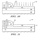
- silicide processing of wafer 100 is performed by depositing a metal such as cobalt that is reactive with silicon over wafer 100.
- the wafer is then heated to react the metal with silicon (where the metal overlies silicon) to form silicide structures identified by reference numeral 150 in a manner that will be familiar to those skilled in semiconductor wafer fabrication.
- Silicide 150 forms overlying the elevated source/drain region 130 as well as overlying silicon gate 110. In the depicted embodiment, the silicide 150 extends entirely through the elevated source/drain 132 and partially into the underlying silicon layer 108.
- the resulting transistor 160 includes a gate electrode 110 overlying a transistor channel region 162.
- a silicided and elevated source/drain region is laterally displaced from gate electrode 110.
- An offset spacer 122 and a replacement spacer 136, both comprised of silicon nitride are located between gate electrode 110 and elevated source/drain 132.
- a first liner oxide 120 is located between offset spacer 122 and gate electrode 110 while the third liner oxide 134 is positioned between offset spacer 122 and replacement spacer 136.
- the specified thickness for the various films and the source gas for the epitaxial formation of elevated source/drain 132 may be different than those specified herein.
- Another example of an alternative is to substitute a different metal for the silicide processing described with respect to FIG. 11 .
Landscapes
- Insulated Gate Type Field-Effect Transistor (AREA)
- Electrodes Of Semiconductors (AREA)
- Thin Film Transistor (AREA)
- Junction Field-Effect Transistors (AREA)
Applications Claiming Priority (2)
| Application Number | Priority Date | Filing Date | Title |
|---|---|---|---|
| US10/839,385 US7125805B2 (en) | 2004-05-05 | 2004-05-05 | Method of semiconductor fabrication incorporating disposable spacer into elevated source/drain processing |
| PCT/US2005/012252 WO2005112099A2 (en) | 2004-05-05 | 2005-04-13 | Method of semiconductor fabrication in corporating disposable spacer into elevated source/drain processing |
Publications (3)
| Publication Number | Publication Date |
|---|---|
| EP1756860A2 EP1756860A2 (en) | 2007-02-28 |
| EP1756860A4 EP1756860A4 (en) | 2008-12-17 |
| EP1756860B1 true EP1756860B1 (en) | 2009-11-04 |
Family
ID=35239953
Family Applications (1)
| Application Number | Title | Priority Date | Filing Date |
|---|---|---|---|
| EP05735763A Expired - Lifetime EP1756860B1 (en) | 2004-05-05 | 2005-04-13 | Method of semiconductor fabrication in corporating disposable spacer into elevated source/drain processing |
Country Status (9)
| Country | Link |
|---|---|
| US (1) | US7125805B2 (enExample) |
| EP (1) | EP1756860B1 (enExample) |
| JP (1) | JP5048480B2 (enExample) |
| KR (1) | KR20070007900A (enExample) |
| CN (1) | CN1998072B (enExample) |
| AT (1) | ATE447765T1 (enExample) |
| DE (1) | DE602005017490D1 (enExample) |
| TW (1) | TWI377625B (enExample) |
| WO (1) | WO2005112099A2 (enExample) |
Families Citing this family (16)
| Publication number | Priority date | Publication date | Assignee | Title |
|---|---|---|---|---|
| KR100668954B1 (ko) * | 2004-12-15 | 2007-01-12 | 동부일렉트로닉스 주식회사 | 박막트랜지스터 제조 방법 |
| US7745296B2 (en) * | 2005-06-08 | 2010-06-29 | Globalfoundries Inc. | Raised source and drain process with disposable spacers |
| US20070056930A1 (en) * | 2005-09-14 | 2007-03-15 | International Business Machines Corporation | Polysilicon etching methods |
| US7514331B2 (en) * | 2006-06-08 | 2009-04-07 | Texas Instruments Incorporated | Method of manufacturing gate sidewalls that avoids recessing |
| US7510923B2 (en) * | 2006-12-19 | 2009-03-31 | Texas Instruments Incorporated | Slim spacer implementation to improve drive current |
| US7550808B2 (en) * | 2007-01-18 | 2009-06-23 | International Business Machines Corporation | Fully siliciding regions to improve performance |
| JP2009158677A (ja) * | 2007-12-26 | 2009-07-16 | Renesas Technology Corp | 半導体装置の製造方法及び混成トランジスタ用半導体装置の製造方法 |
| JP6169222B2 (ja) * | 2012-01-23 | 2017-07-26 | ルネサスエレクトロニクス株式会社 | 半導体装置の製造方法 |
| JP5968708B2 (ja) | 2012-01-23 | 2016-08-10 | ルネサスエレクトロニクス株式会社 | 半導体装置 |
| US9171927B2 (en) | 2013-03-26 | 2015-10-27 | GlobalFoundries, Inc. | Spacer replacement for replacement metal gate semiconductor devices |
| CN103412444B (zh) * | 2013-07-23 | 2015-08-26 | 北京京东方光电科技有限公司 | 一种阵列基板及其制作方法和显示面板 |
| JP6279291B2 (ja) * | 2013-11-18 | 2018-02-14 | ルネサスエレクトロニクス株式会社 | 半導体装置の製造方法 |
| US9773865B2 (en) | 2014-09-22 | 2017-09-26 | International Business Machines Corporation | Self-forming spacers using oxidation |
| US11653498B2 (en) * | 2017-11-30 | 2023-05-16 | Taiwan Semiconductor Manufacturing Co., Ltd. | Memory device with improved data retention |
| JP7034834B2 (ja) | 2018-05-30 | 2022-03-14 | ルネサスエレクトロニクス株式会社 | 半導体装置およびその製造方法 |
| US11437245B2 (en) * | 2020-09-30 | 2022-09-06 | Taiwan Semiconductor Manufacturing Company, Ltd. | Germanium hump reduction |
Family Cites Families (12)
| Publication number | Priority date | Publication date | Assignee | Title |
|---|---|---|---|---|
| US5200352A (en) * | 1991-11-25 | 1993-04-06 | Motorola Inc. | Transistor having a lightly doped region and method of formation |
| US5496750A (en) * | 1994-09-19 | 1996-03-05 | Texas Instruments Incorporated | Elevated source/drain junction metal oxide semiconductor field-effect transistor using blanket silicon deposition |
| JP2848299B2 (ja) * | 1995-12-21 | 1999-01-20 | 日本電気株式会社 | 半導体装置及びその製造方法 |
| US5847428A (en) * | 1996-12-06 | 1998-12-08 | Advanced Micro Devices, Inc. | Integrated circuit gate conductor which uses layered spacers to produce a graded junction |
| TW469648B (en) * | 1999-09-07 | 2001-12-21 | Sharp Kk | Semiconductor device and its manufacture method |
| US6555437B1 (en) * | 2001-04-27 | 2003-04-29 | Advanced Micro Devices, Inc. | Multiple halo implant in a MOSFET with raised source/drain structure |
| US20020171107A1 (en) * | 2001-05-21 | 2002-11-21 | Baohong Cheng | Method for forming a semiconductor device having elevated source and drain regions |
| US6429084B1 (en) * | 2001-06-20 | 2002-08-06 | International Business Machines Corporation | MOS transistors with raised sources and drains |
| US6614079B2 (en) * | 2001-07-19 | 2003-09-02 | International Business Machines Corporation | All-in-one disposable/permanent spacer elevated source/drain, self-aligned silicide CMOS |
| JP2004095639A (ja) * | 2002-08-29 | 2004-03-25 | Fujitsu Ltd | 半導体装置及びその製造方法 |
| US6800530B2 (en) * | 2003-01-14 | 2004-10-05 | International Business Machines Corporation | Triple layer hard mask for gate patterning to fabricate scaled CMOS transistors |
| US20050048732A1 (en) * | 2003-08-26 | 2005-03-03 | International Business Machines Corporation | Method to produce transistor having reduced gate height |
-
2004
- 2004-05-05 US US10/839,385 patent/US7125805B2/en not_active Expired - Lifetime
-
2005
- 2005-04-13 EP EP05735763A patent/EP1756860B1/en not_active Expired - Lifetime
- 2005-04-13 CN CN200580014349XA patent/CN1998072B/zh not_active Expired - Fee Related
- 2005-04-13 DE DE602005017490T patent/DE602005017490D1/de not_active Expired - Lifetime
- 2005-04-13 JP JP2007511381A patent/JP5048480B2/ja not_active Expired - Fee Related
- 2005-04-13 AT AT05735763T patent/ATE447765T1/de not_active IP Right Cessation
- 2005-04-13 WO PCT/US2005/012252 patent/WO2005112099A2/en not_active Ceased
- 2005-04-13 KR KR1020067023143A patent/KR20070007900A/ko not_active Withdrawn
- 2005-05-05 TW TW094114573A patent/TWI377625B/zh not_active IP Right Cessation
Also Published As
| Publication number | Publication date |
|---|---|
| US20050250287A1 (en) | 2005-11-10 |
| WO2005112099A3 (en) | 2006-04-27 |
| TW200625463A (en) | 2006-07-16 |
| CN1998072B (zh) | 2010-09-15 |
| JP2007536734A (ja) | 2007-12-13 |
| TWI377625B (en) | 2012-11-21 |
| EP1756860A2 (en) | 2007-02-28 |
| KR20070007900A (ko) | 2007-01-16 |
| JP5048480B2 (ja) | 2012-10-17 |
| WO2005112099A2 (en) | 2005-11-24 |
| ATE447765T1 (de) | 2009-11-15 |
| EP1756860A4 (en) | 2008-12-17 |
| US7125805B2 (en) | 2006-10-24 |
| DE602005017490D1 (de) | 2009-12-17 |
| CN1998072A (zh) | 2007-07-11 |
Similar Documents
| Publication | Publication Date | Title |
|---|---|---|
| EP1756860B1 (en) | Method of semiconductor fabrication in corporating disposable spacer into elevated source/drain processing | |
| US7867860B2 (en) | Strained channel transistor formation | |
| US6627488B2 (en) | Method for fabricating a semiconductor device using a damascene process | |
| US8324038B2 (en) | Method of removing a spacer, method of manufacturing a metal-oxide-semiconductor transistor device, and metal-oxide-semiconductor transistor device | |
| US6303450B1 (en) | CMOS device structures and method of making same | |
| US7397091B2 (en) | SiGe nickel barrier structure employed in a CMOS device to prevent excess diffusion of nickel used in the silicide material | |
| US20070215951A1 (en) | Semiconductor devices having silicided electrodes | |
| US6900092B2 (en) | Surface engineering to prevent epi growth on gate poly during selective epi processing | |
| US6589836B1 (en) | One step dual salicide formation for ultra shallow junction applications | |
| US7485516B2 (en) | Method of ion implantation of nitrogen into semiconductor substrate prior to oxidation for offset spacer formation | |
| US6235600B1 (en) | Method for improving hot carrier lifetime via a nitrogen implantation procedure performed before or after a teos liner deposition | |
| US7732289B2 (en) | Method of forming a MOS device with an additional layer | |
| US9064891B2 (en) | Gate encapsulation achieved by single-step deposition | |
| US9087716B2 (en) | Channel semiconductor alloy layer growth adjusted by impurity ion implantation | |
| US5879999A (en) | Method of manufacturing an insulated gate semiconductor device having a spacer extension | |
| US20030170958A1 (en) | Method of manufacturing semiconductor device | |
| US5747852A (en) | LDD MOS transistor with improved uniformity and controllability of alignment | |
| JP4541125B2 (ja) | 高誘電率ゲート絶縁膜を備えた電界効果トランジスタを有する半導体装置及びその製造方法 | |
| US6667233B2 (en) | Method for forming a silicide layer of semiconductor device | |
| CN1934686B (zh) | 场效应晶体管及场效应晶体管的制造方法 | |
| KR100685898B1 (ko) | 반도체 소자의 제조방법 |
Legal Events
| Date | Code | Title | Description |
|---|---|---|---|
| PUAI | Public reference made under article 153(3) epc to a published international application that has entered the european phase |
Free format text: ORIGINAL CODE: 0009012 |
|
| 17P | Request for examination filed |
Effective date: 20061107 |
|
| AK | Designated contracting states |
Kind code of ref document: A2 Designated state(s): AT BE BG CH CY CZ DE DK EE ES FI FR GB GR HU IE IS IT LI LT LU MC NL PL PT RO SE SI SK TR |
|
| DAX | Request for extension of the european patent (deleted) | ||
| A4 | Supplementary search report drawn up and despatched |
Effective date: 20081119 |
|
| GRAP | Despatch of communication of intention to grant a patent |
Free format text: ORIGINAL CODE: EPIDOSNIGR1 |
|
| GRAS | Grant fee paid |
Free format text: ORIGINAL CODE: EPIDOSNIGR3 |
|
| GRAA | (expected) grant |
Free format text: ORIGINAL CODE: 0009210 |
|
| AK | Designated contracting states |
Kind code of ref document: B1 Designated state(s): AT BE BG CH CY CZ DE DK EE ES FI FR GB GR HU IE IS IT LI LT LU MC NL PL PT RO SE SI SK TR |
|
| REG | Reference to a national code |
Ref country code: GB Ref legal event code: FG4D |
|
| REG | Reference to a national code |
Ref country code: CH Ref legal event code: EP |
|
| REG | Reference to a national code |
Ref country code: IE Ref legal event code: FG4D |
|
| REF | Corresponds to: |
Ref document number: 602005017490 Country of ref document: DE Date of ref document: 20091217 Kind code of ref document: P |
|
| NLV1 | Nl: lapsed or annulled due to failure to fulfill the requirements of art. 29p and 29m of the patents act | ||
| LTIE | Lt: invalidation of european patent or patent extension |
Effective date: 20091104 |
|
| PG25 | Lapsed in a contracting state [announced via postgrant information from national office to epo] |
Ref country code: PT Free format text: LAPSE BECAUSE OF FAILURE TO SUBMIT A TRANSLATION OF THE DESCRIPTION OR TO PAY THE FEE WITHIN THE PRESCRIBED TIME-LIMIT Effective date: 20100304 Ref country code: FI Free format text: LAPSE BECAUSE OF FAILURE TO SUBMIT A TRANSLATION OF THE DESCRIPTION OR TO PAY THE FEE WITHIN THE PRESCRIBED TIME-LIMIT Effective date: 20091104 Ref country code: ES Free format text: LAPSE BECAUSE OF FAILURE TO SUBMIT A TRANSLATION OF THE DESCRIPTION OR TO PAY THE FEE WITHIN THE PRESCRIBED TIME-LIMIT Effective date: 20100215 Ref country code: SE Free format text: LAPSE BECAUSE OF FAILURE TO SUBMIT A TRANSLATION OF THE DESCRIPTION OR TO PAY THE FEE WITHIN THE PRESCRIBED TIME-LIMIT Effective date: 20091104 Ref country code: IS Free format text: LAPSE BECAUSE OF FAILURE TO SUBMIT A TRANSLATION OF THE DESCRIPTION OR TO PAY THE FEE WITHIN THE PRESCRIBED TIME-LIMIT Effective date: 20100304 Ref country code: LT Free format text: LAPSE BECAUSE OF FAILURE TO SUBMIT A TRANSLATION OF THE DESCRIPTION OR TO PAY THE FEE WITHIN THE PRESCRIBED TIME-LIMIT Effective date: 20091104 |
|
| PG25 | Lapsed in a contracting state [announced via postgrant information from national office to epo] |
Ref country code: CY Free format text: LAPSE BECAUSE OF FAILURE TO SUBMIT A TRANSLATION OF THE DESCRIPTION OR TO PAY THE FEE WITHIN THE PRESCRIBED TIME-LIMIT Effective date: 20091104 Ref country code: PL Free format text: LAPSE BECAUSE OF FAILURE TO SUBMIT A TRANSLATION OF THE DESCRIPTION OR TO PAY THE FEE WITHIN THE PRESCRIBED TIME-LIMIT Effective date: 20091104 Ref country code: SI Free format text: LAPSE BECAUSE OF FAILURE TO SUBMIT A TRANSLATION OF THE DESCRIPTION OR TO PAY THE FEE WITHIN THE PRESCRIBED TIME-LIMIT Effective date: 20091104 |
|
| PG25 | Lapsed in a contracting state [announced via postgrant information from national office to epo] |
Ref country code: BE Free format text: LAPSE BECAUSE OF FAILURE TO SUBMIT A TRANSLATION OF THE DESCRIPTION OR TO PAY THE FEE WITHIN THE PRESCRIBED TIME-LIMIT Effective date: 20091104 Ref country code: AT Free format text: LAPSE BECAUSE OF FAILURE TO SUBMIT A TRANSLATION OF THE DESCRIPTION OR TO PAY THE FEE WITHIN THE PRESCRIBED TIME-LIMIT Effective date: 20091104 |
|
| PG25 | Lapsed in a contracting state [announced via postgrant information from national office to epo] |
Ref country code: DK Free format text: LAPSE BECAUSE OF FAILURE TO SUBMIT A TRANSLATION OF THE DESCRIPTION OR TO PAY THE FEE WITHIN THE PRESCRIBED TIME-LIMIT Effective date: 20091104 Ref country code: EE Free format text: LAPSE BECAUSE OF FAILURE TO SUBMIT A TRANSLATION OF THE DESCRIPTION OR TO PAY THE FEE WITHIN THE PRESCRIBED TIME-LIMIT Effective date: 20091104 Ref country code: RO Free format text: LAPSE BECAUSE OF FAILURE TO SUBMIT A TRANSLATION OF THE DESCRIPTION OR TO PAY THE FEE WITHIN THE PRESCRIBED TIME-LIMIT Effective date: 20091104 Ref country code: BG Free format text: LAPSE BECAUSE OF FAILURE TO SUBMIT A TRANSLATION OF THE DESCRIPTION OR TO PAY THE FEE WITHIN THE PRESCRIBED TIME-LIMIT Effective date: 20100204 |
|
| PG25 | Lapsed in a contracting state [announced via postgrant information from national office to epo] |
Ref country code: CZ Free format text: LAPSE BECAUSE OF FAILURE TO SUBMIT A TRANSLATION OF THE DESCRIPTION OR TO PAY THE FEE WITHIN THE PRESCRIBED TIME-LIMIT Effective date: 20091104 Ref country code: SK Free format text: LAPSE BECAUSE OF FAILURE TO SUBMIT A TRANSLATION OF THE DESCRIPTION OR TO PAY THE FEE WITHIN THE PRESCRIBED TIME-LIMIT Effective date: 20091104 |
|
| PLBE | No opposition filed within time limit |
Free format text: ORIGINAL CODE: 0009261 |
|
| STAA | Information on the status of an ep patent application or granted ep patent |
Free format text: STATUS: NO OPPOSITION FILED WITHIN TIME LIMIT |
|
| 26N | No opposition filed |
Effective date: 20100805 |
|
| PG25 | Lapsed in a contracting state [announced via postgrant information from national office to epo] |
Ref country code: GR Free format text: LAPSE BECAUSE OF FAILURE TO SUBMIT A TRANSLATION OF THE DESCRIPTION OR TO PAY THE FEE WITHIN THE PRESCRIBED TIME-LIMIT Effective date: 20100205 |
|
| PG25 | Lapsed in a contracting state [announced via postgrant information from national office to epo] |
Ref country code: MC Free format text: LAPSE BECAUSE OF NON-PAYMENT OF DUE FEES Effective date: 20100430 |
|
| REG | Reference to a national code |
Ref country code: CH Ref legal event code: PL |
|
| PG25 | Lapsed in a contracting state [announced via postgrant information from national office to epo] |
Ref country code: IE Free format text: LAPSE BECAUSE OF NON-PAYMENT OF DUE FEES Effective date: 20100413 |
|
| PG25 | Lapsed in a contracting state [announced via postgrant information from national office to epo] |
Ref country code: CH Free format text: LAPSE BECAUSE OF NON-PAYMENT OF DUE FEES Effective date: 20100430 Ref country code: LI Free format text: LAPSE BECAUSE OF NON-PAYMENT OF DUE FEES Effective date: 20100430 |
|
| PG25 | Lapsed in a contracting state [announced via postgrant information from national office to epo] |
Ref country code: HU Free format text: LAPSE BECAUSE OF FAILURE TO SUBMIT A TRANSLATION OF THE DESCRIPTION OR TO PAY THE FEE WITHIN THE PRESCRIBED TIME-LIMIT Effective date: 20100505 Ref country code: NL Free format text: LAPSE BECAUSE OF FAILURE TO SUBMIT A TRANSLATION OF THE DESCRIPTION OR TO PAY THE FEE WITHIN THE PRESCRIBED TIME-LIMIT Effective date: 20091104 Ref country code: LU Free format text: LAPSE BECAUSE OF NON-PAYMENT OF DUE FEES Effective date: 20100413 |
|
| PG25 | Lapsed in a contracting state [announced via postgrant information from national office to epo] |
Ref country code: TR Free format text: LAPSE BECAUSE OF FAILURE TO SUBMIT A TRANSLATION OF THE DESCRIPTION OR TO PAY THE FEE WITHIN THE PRESCRIBED TIME-LIMIT Effective date: 20091104 |
|
| PGFP | Annual fee paid to national office [announced via postgrant information from national office to epo] |
Ref country code: GB Payment date: 20140428 Year of fee payment: 10 |
|
| PGFP | Annual fee paid to national office [announced via postgrant information from national office to epo] |
Ref country code: FR Payment date: 20140417 Year of fee payment: 10 Ref country code: IT Payment date: 20140424 Year of fee payment: 10 |
|
| GBPC | Gb: european patent ceased through non-payment of renewal fee |
Effective date: 20150413 |
|
| PG25 | Lapsed in a contracting state [announced via postgrant information from national office to epo] |
Ref country code: IT Free format text: LAPSE BECAUSE OF NON-PAYMENT OF DUE FEES Effective date: 20150413 Ref country code: GB Free format text: LAPSE BECAUSE OF NON-PAYMENT OF DUE FEES Effective date: 20150413 |
|
| REG | Reference to a national code |
Ref country code: FR Ref legal event code: ST Effective date: 20151231 |
|
| PG25 | Lapsed in a contracting state [announced via postgrant information from national office to epo] |
Ref country code: FR Free format text: LAPSE BECAUSE OF NON-PAYMENT OF DUE FEES Effective date: 20150430 |
|
| REG | Reference to a national code |
Ref country code: DE Ref legal event code: R081 Ref document number: 602005017490 Country of ref document: DE Owner name: NXP USA, INC. (N.D.GES.D.STAATES DELAWARE), AU, US Free format text: FORMER OWNER: FREESCALE SEMICONDUCTOR, INC., AUSTIN, TEX., US |
|
| PGFP | Annual fee paid to national office [announced via postgrant information from national office to epo] |
Ref country code: DE Payment date: 20180320 Year of fee payment: 14 |
|
| REG | Reference to a national code |
Ref country code: DE Ref legal event code: R119 Ref document number: 602005017490 Country of ref document: DE |
|
| PG25 | Lapsed in a contracting state [announced via postgrant information from national office to epo] |
Ref country code: DE Free format text: LAPSE BECAUSE OF NON-PAYMENT OF DUE FEES Effective date: 20191101 |