EP1702365B1 - Amelioration de mobilites d'electrons et de trous en silicium 110 sous contrainte compressive biaxiale - Google Patents
Amelioration de mobilites d'electrons et de trous en silicium 110 sous contrainte compressive biaxiale Download PDFInfo
- Publication number
- EP1702365B1 EP1702365B1 EP04822326A EP04822326A EP1702365B1 EP 1702365 B1 EP1702365 B1 EP 1702365B1 EP 04822326 A EP04822326 A EP 04822326A EP 04822326 A EP04822326 A EP 04822326A EP 1702365 B1 EP1702365 B1 EP 1702365B1
- Authority
- EP
- European Patent Office
- Prior art keywords
- layer
- silicon
- containing layer
- porous
- substrate
- Prior art date
- Legal status (The legal status is an assumption and is not a legal conclusion. Google has not performed a legal analysis and makes no representation as to the accuracy of the status listed.)
- Expired - Lifetime
Links
Images



Classifications
-
- H—ELECTRICITY
- H10—SEMICONDUCTOR DEVICES; ELECTRIC SOLID-STATE DEVICES NOT OTHERWISE PROVIDED FOR
- H10D—INORGANIC ELECTRIC SEMICONDUCTOR DEVICES
- H10D30/00—Field-effect transistors [FET]
- H10D30/60—Insulated-gate field-effect transistors [IGFET]
- H10D30/791—Arrangements for exerting mechanical stress on the crystal lattice of the channel regions
-
- H—ELECTRICITY
- H10—SEMICONDUCTOR DEVICES; ELECTRIC SOLID-STATE DEVICES NOT OTHERWISE PROVIDED FOR
- H10D—INORGANIC ELECTRIC SEMICONDUCTOR DEVICES
- H10D62/00—Semiconductor bodies, or regions thereof, of devices having potential barriers
- H10D62/40—Crystalline structures
-
- H—ELECTRICITY
- H10—SEMICONDUCTOR DEVICES; ELECTRIC SOLID-STATE DEVICES NOT OTHERWISE PROVIDED FOR
- H10D—INORGANIC ELECTRIC SEMICONDUCTOR DEVICES
- H10D30/00—Field-effect transistors [FET]
- H10D30/01—Manufacture or treatment
- H10D30/021—Manufacture or treatment of FETs having insulated gates [IGFET]
- H10D30/0223—Manufacture or treatment of FETs having insulated gates [IGFET] having source and drain regions or source and drain extensions self-aligned to sides of the gate
- H10D30/0227—Manufacture or treatment of FETs having insulated gates [IGFET] having source and drain regions or source and drain extensions self-aligned to sides of the gate having both lightly-doped source and drain extensions and source and drain regions self-aligned to the sides of the gate, e.g. lightly-doped drain [LDD] MOSFET or double-diffused drain [DDD] MOSFET
-
- H—ELECTRICITY
- H10—SEMICONDUCTOR DEVICES; ELECTRIC SOLID-STATE DEVICES NOT OTHERWISE PROVIDED FOR
- H10D—INORGANIC ELECTRIC SEMICONDUCTOR DEVICES
- H10D30/00—Field-effect transistors [FET]
- H10D30/60—Insulated-gate field-effect transistors [IGFET]
- H10D30/601—Insulated-gate field-effect transistors [IGFET] having lightly-doped drain or source extensions, e.g. LDD IGFETs or DDD IGFETs
-
- H—ELECTRICITY
- H10—SEMICONDUCTOR DEVICES; ELECTRIC SOLID-STATE DEVICES NOT OTHERWISE PROVIDED FOR
- H10D—INORGANIC ELECTRIC SEMICONDUCTOR DEVICES
- H10D30/00—Field-effect transistors [FET]
- H10D30/60—Insulated-gate field-effect transistors [IGFET]
- H10D30/67—Thin-film transistors [TFT]
- H10D30/674—Thin-film transistors [TFT] characterised by the active materials
- H10D30/6741—Group IV materials, e.g. germanium or silicon carbide
-
- H—ELECTRICITY
- H10—SEMICONDUCTOR DEVICES; ELECTRIC SOLID-STATE DEVICES NOT OTHERWISE PROVIDED FOR
- H10D—INORGANIC ELECTRIC SEMICONDUCTOR DEVICES
- H10D30/00—Field-effect transistors [FET]
- H10D30/60—Insulated-gate field-effect transistors [IGFET]
- H10D30/791—Arrangements for exerting mechanical stress on the crystal lattice of the channel regions
- H10D30/792—Arrangements for exerting mechanical stress on the crystal lattice of the channel regions comprising applied insulating layers, e.g. stress liners
-
- H—ELECTRICITY
- H10—SEMICONDUCTOR DEVICES; ELECTRIC SOLID-STATE DEVICES NOT OTHERWISE PROVIDED FOR
- H10D—INORGANIC ELECTRIC SEMICONDUCTOR DEVICES
- H10D30/00—Field-effect transistors [FET]
- H10D30/60—Insulated-gate field-effect transistors [IGFET]
- H10D30/791—Arrangements for exerting mechanical stress on the crystal lattice of the channel regions
- H10D30/795—Arrangements for exerting mechanical stress on the crystal lattice of the channel regions being in lateral device isolation regions, e.g. STI
-
- H—ELECTRICITY
- H10—SEMICONDUCTOR DEVICES; ELECTRIC SOLID-STATE DEVICES NOT OTHERWISE PROVIDED FOR
- H10D—INORGANIC ELECTRIC SEMICONDUCTOR DEVICES
- H10D62/00—Semiconductor bodies, or regions thereof, of devices having potential barriers
- H10D62/40—Crystalline structures
- H10D62/405—Orientations of crystalline planes
-
- H—ELECTRICITY
- H10—SEMICONDUCTOR DEVICES; ELECTRIC SOLID-STATE DEVICES NOT OTHERWISE PROVIDED FOR
- H10D—INORGANIC ELECTRIC SEMICONDUCTOR DEVICES
- H10D84/00—Integrated devices formed in or on semiconductor substrates that comprise only semiconducting layers, e.g. on Si wafers or on GaAs-on-Si wafers
- H10D84/01—Manufacture or treatment
- H10D84/0123—Integrating together multiple components covered by H10D12/00 or H10D30/00, e.g. integrating multiple IGBTs
- H10D84/0126—Integrating together multiple components covered by H10D12/00 or H10D30/00, e.g. integrating multiple IGBTs the components including insulated gates, e.g. IGFETs
- H10D84/0165—Integrating together multiple components covered by H10D12/00 or H10D30/00, e.g. integrating multiple IGBTs the components including insulated gates, e.g. IGFETs the components including complementary IGFETs, e.g. CMOS devices
- H10D84/0167—Manufacturing their channels
-
- H—ELECTRICITY
- H10—SEMICONDUCTOR DEVICES; ELECTRIC SOLID-STATE DEVICES NOT OTHERWISE PROVIDED FOR
- H10D—INORGANIC ELECTRIC SEMICONDUCTOR DEVICES
- H10D84/00—Integrated devices formed in or on semiconductor substrates that comprise only semiconducting layers, e.g. on Si wafers or on GaAs-on-Si wafers
- H10D84/01—Manufacture or treatment
- H10D84/02—Manufacture or treatment characterised by using material-based technologies
- H10D84/03—Manufacture or treatment characterised by using material-based technologies using Group IV technology, e.g. silicon technology or silicon-carbide [SiC] technology
- H10D84/038—Manufacture or treatment characterised by using material-based technologies using Group IV technology, e.g. silicon technology or silicon-carbide [SiC] technology using silicon technology, e.g. SiGe
-
- H—ELECTRICITY
- H10—SEMICONDUCTOR DEVICES; ELECTRIC SOLID-STATE DEVICES NOT OTHERWISE PROVIDED FOR
- H10F—INORGANIC SEMICONDUCTOR DEVICES SENSITIVE TO INFRARED RADIATION, LIGHT, ELECTROMAGNETIC RADIATION OF SHORTER WAVELENGTH OR CORPUSCULAR RADIATION
- H10F30/00—Individual radiation-sensitive semiconductor devices in which radiation controls the flow of current through the devices, e.g. photodetectors
- H10F30/20—Individual radiation-sensitive semiconductor devices in which radiation controls the flow of current through the devices, e.g. photodetectors the devices having potential barriers, e.g. phototransistors
- H10F30/21—Individual radiation-sensitive semiconductor devices in which radiation controls the flow of current through the devices, e.g. photodetectors the devices having potential barriers, e.g. phototransistors the devices being sensitive to infrared, visible or ultraviolet radiation
- H10F30/22—Individual radiation-sensitive semiconductor devices in which radiation controls the flow of current through the devices, e.g. photodetectors the devices having potential barriers, e.g. phototransistors the devices being sensitive to infrared, visible or ultraviolet radiation the devices having only one potential barrier, e.g. photodiodes
- H10F30/222—Individual radiation-sensitive semiconductor devices in which radiation controls the flow of current through the devices, e.g. photodetectors the devices having potential barriers, e.g. phototransistors the devices being sensitive to infrared, visible or ultraviolet radiation the devices having only one potential barrier, e.g. photodiodes the potential barrier being a PN heterojunction
-
- H—ELECTRICITY
- H10—SEMICONDUCTOR DEVICES; ELECTRIC SOLID-STATE DEVICES NOT OTHERWISE PROVIDED FOR
- H10W—GENERIC PACKAGES, INTERCONNECTIONS, CONNECTORS OR OTHER CONSTRUCTIONAL DETAILS OF DEVICES COVERED BY CLASS H10
- H10W10/00—Isolation regions in semiconductor bodies between components of integrated devices
- H10W10/01—Manufacture or treatment
- H10W10/011—Manufacture or treatment of isolation regions comprising dielectric materials
-
- H—ELECTRICITY
- H10—SEMICONDUCTOR DEVICES; ELECTRIC SOLID-STATE DEVICES NOT OTHERWISE PROVIDED FOR
- H10W—GENERIC PACKAGES, INTERCONNECTIONS, CONNECTORS OR OTHER CONSTRUCTIONAL DETAILS OF DEVICES COVERED BY CLASS H10
- H10W10/00—Isolation regions in semiconductor bodies between components of integrated devices
- H10W10/10—Isolation regions comprising dielectric materials
Definitions
- the present invention relates to semiconductor materials having enhanced electron and hole mobilities, and more particularly, to semiconductor materials that include a silicon (Si)-containing layer having enhanced electron and hole mobilities.
- the present invention also provides a method of forming such semiconductor materials.
- MOSFETs silicon metal oxide semiconductor field effect transistors
- IRS International Technology Roadmap for Semiconductors
- CMOS complementary metal oxide semiconductor
- a preferred embodiment of the present invention provides a semiconductor material that has enhanced carrier mobilities that comprises a Si-containing layer having a ⁇ 110> crystal orientation that is under a biaxial compressive strain.
- biaxial compressive strain is used herein to describe the net stress caused by longitudinal compressive stress and lateral (or transverse) compressive stress that is induced in the plane of the Si-containing layer during the manufacturing of the semiconductor material.
- a semiconductor material comprising a silicon-containing layer having a ⁇ 110> crystal orientation, said silicon-containing layer is under a biaxial compressive strain characterised by the silicon-containing layer overlying a substrate having a coefficient of thermal expansion that is greater than the coefficient of thermal expansion of silicon.
- a method for forming a silicon-containing semiconductor material comprising the steps of: providing a silicon-containing layer; bonding the silicon-containing layer to a substrate having a coefficient of thermal expansion that is greater than the coefficient of thermal expansion of silicon; during the bonding, heating the silicon-containing layer and the substrate to an elevated temperature; and thereafter, cooling the bonded silicon-containing layer and substrate to create a biaxial compressive strain in said silicon-containing layer.
- the Si-containing layer is preferably a crystalline Si-containing layer comprising Si or SiGe.
- the creating a biaxial compressive strain preferably comprises forming at least one porous Si layer having an uppermost surface in said ⁇ 110> Si-containing layer; annealing the uppermost surface to create a non-porous surface layer; forming a crystalline epitaxial Si-containing layer having a ⁇ 110> orientation on the non-porous surface layer thereby forming a transfer structure; bonding the transfer structure to a material that has a higher coefficient of thermal expansion than Si at a temperature that is elevated above the ultimate device operating temperature to provide a bonded structure; cooling the bonded structure so that a mechanically weak interface forms at said at least one porous Si layer thereby cleaving said bonded structure at said interface; and removing remaining portions of the least one porous Si layer from the cleaved structure.
- the at least one porous Si layer preferably comprises an electrolytic anodization process.
- the anodization process preferably includes utilizing an HF-containing solution.
- the annealing is preferably performed at a temperature from about 900° to about 1150°C.
- the forming said crystalline epitaxial Si-containing layer may comprise an epitaxial growth process.
- the epitaxial growth process preferably comprises an UHVCVD process.
- the method may further comprise forming an oxide layer on said crystalline Si-containing layer prior to bonding.
- the bonding preferably comprises bringing that transfer structure and said material together, optionally applying an external force, and heating.
- the heating is preferably performed at a temperature from about 400° to about 1000°C.
- the cooling is preferably performed at a rate of about 50°C/min or less.
- the removing preferably comprises a wet etching process.
- the method may further comprise smoothing said crystalline epitaxial Si-containing that is under biaxial compressive strain by annealing in a H 2 -containing ambient at a temperature of from about 850° to about 1100°C.
- a method for forming a silicon-containing semiconductor material comprising the steps of: forming at least one porous Si layer having an uppermost surface in a ⁇ 110> Si-containing substrate; annealing the uppermost surface to create a non-porous surface layer; forming a crystalline epitaxial Si-containing layer having a ⁇ 110> orientation on the non-porous surface layer thereby forming a transfer structure; bonding the transfer structure to a material that has a higher coefficient of thermal expansion than Si at a temperature that is elevated above the ultimate device operating temperature to provide a bonded structure; cooling the bonded structure so that a mechanically weak interface forms at said at least one porous Si layer thereby cleaving said bonded structure at said interface; and removing remaining portions of the least one porous Si layer from the cleaved structure so as to provide a semiconductor material that includes at least the crystalline epitaxial Si-containing layer having a ⁇ 110> orientation atop said material, said
- An example of a semiconductor material embodying the present invention that includes a ⁇ 110> Si-containing layer with biaxial compressive strain provides enhanced mobilities for both nMOS and pMOS.
- Another example of the present invention relates to a method of forming such a semiconductor material. Specifically and in broad terms, a method embodying the present invention includes the steps of providing a silicon-containing ⁇ 110> layer; and creating a biaxial compressive strain in the silicon-containing ⁇ 110> layer.
- the Si-containing layer having the ⁇ 110> orientation and biaxial compressive strain is created by a method that includes the steps of: forming at least one porous Si layer having an uppermost surface in a ⁇ 110> Si-containing substrate; annealing the uppermost surface so as to create a non-porous surface layer; forming a crystalline epitaxial Si-containing layer having a ⁇ 110> orientation on the non-porous surface layer thereby forming a transfer structure; bonding the transfer structure to a material that has a higher coefficient of thermal expansion than Si at a temperature that is elevated above the ultimate device operating temperature to provide a bonded structure; cooling the bonded structure so that a mechanically weak interface forms at said at least one porous Si layer thereby cleaving said bonded structure at said interface; and removing remaining portions of the least one porous Si layer from the cleaved structure to provide a semiconductor material that includes at least the crystalline epitaxial Si-containing layer having a ⁇ 110> orientation atop said material, said
- a preferred embodiment of the present invention provides a semiconductor material comprising a Si-containing layer having a ⁇ 110> crystal orientation and biaxial compressive strain and a method of forming the same, will now be described in greater detail by referring to the accompanying drawings.
- the applicants have determined through numerical calculations that when a significant (greater than about 0.2%, preferably greater than about 0.5%) biaxial compressive strain is introduced in a ⁇ 110> Si-containing layer, both the electron and hole mobilities exceed those in the conventional unstrained ⁇ 100> Si case.
- the % strain is defined herein as the percentage change in the crystalline lattice constant of a material in a given direction.
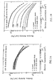
- FIGS. 1A-1B and FIGS. 2A-2B The results of the above calculations, which have been determined by computing the carrier mobilities using the Kubo-Greenwood formula (which results from a solution of the linearized Boltzmann transport equation) for carriers in inversion layers is shown in FIGS. 1A-1B and FIGS. 2A-2B .
- the sub-band structure has been calculated using a model band structure consisting of six ellipsoidal conduction-band valleys (with first-order nonparabolic corrections following Kane) for nFETs, or by solving the six-band k*p Hamiltonian (3 bands times 2 spin states) with spin-orbit interaction for the pFETs.
- FIG. 1A shows the calculated electron mobility in the inversion layer of nFETs (as a function of carrier sheet density) for a more common Si ⁇ 100> wafer surface along the [110] crystallographic direction, usually employed in present VLSI technology.
- the application of 1% biaxial tensile strain shows the well-known enhancement of the electron mobility at low electron densities.
- FIG. 1B shows that even moderate amounts of compressive strain (0.5% or larger) for ⁇ 110> surfaces boosts the electron mobility (along the [110] direction) above and beyond the values attained at all densities for the relaxed or strained ⁇ 100> surface.
- FIGS. 2A-2B present analogous information regarding the calculated hole mobility for ⁇ 100> ( FIG. 2A ) and ⁇ 110> ( FIG. 2B ) Si surfaces.
- the application of 1% compressive strain on ⁇ 110> surfaces boosts the hole mobility along the [110] direction by a factor of approximately 3 over the hole mobility for the relaxed ⁇ 100> Si surface.
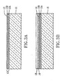
- FIGS. 3A-3E illustrate one method that can be employed in the present invention through which a biaxial compressive strain (greater than about 0.2%, preferably greater than about 0.5%) can be introduced into a ⁇ 110> Si-containing layer in order to achieve these significantly higher carrier mobilities.
- FIG. 3A illustrates an initial structure that can be used in forming the inventive substrate material of the present invention.
- the initial structure shown in FIG. 3A includes a ⁇ 110> Si-containing substrate 10 having at least one porous Si layer 12 formed on the surface of Si-containing substrate 10.
- the at least one porous Si layer 12 has an uppermost surface layer 13.
- two porous Si layers 12A and 12B are formed. Despite showing the presence of two porous Si layers 12A and 12B, the present invention works equally well when only one porous Si layer or more than two porous Si layers are formed.
- Si-containing substrate is used in the present invention to denote a semiconductor material that includes Si.
- Illustrative examples of such Si-containing materials that can be employed as substrate 10 include bulk Si, SiGe having a Ge content of about 25% or less, silicon-on-insulators (SOIs) and SiGe-on-insulators.
- SOIs silicon-on-insulators
- SiGe-on-insulators The substrates can be doped or undoped.
- the at least one porous Si layer is formed in the present invention by utilizing an electrolytic anodization process that is capable of converting a surface portion of the ⁇ 110> Si-containing substrate 10 into a porous Si layer.
- the anodization process is performed by immersing the ⁇ 110> Si-containing substrate 10 into an HF-containing solution while an electrical bias is applied to the ⁇ 110> Si-containing substrate 10 with respect to an electrode also placed in the HF-containing solution.
- the ⁇ 110> Si-containing substrate 10 itself typically serves as the positive electrode of the electrochemical cell, while another semiconducting material such as Si, or a metal is employed as the negative electrode.
- the anodization process used in forming the porous Si layers can also be referred to as an anodic etching process.
- the porous Si layers created using the anodization process are mechanically weak as compared to the remainder of the Si-containing substrate 10, yet the porous Si layers preserve the crystalline quality and orientation of the Si-containing substrate 10.
- porous Si layer 12 when more than one porous Si layer 12 is formed, the other porous layers can have the same or different pore morphology. Porous Si layers containing different pore morphologies can be formed in the present invention by changing the current flow conditions during the anodization process.
- the HF anodization converts a surface region of the Si-containing substrate 10 into porous Si.
- the rate of formation and the nature of the porous Si so-formed are determined by both the material properties as well as the reaction conditions of the anodization process itself (current density, bias, illumination and additives in the HF-containing solution).
- the porous Si layers 12A and 12B formed in the present invention have a porosity of about 0.1% or higher.
- each porous Si layer 12 may vary depending on the anodization conditions employed. Typically, the thickness of each porous Si layer 12 formed in the present invention is from about 100 nm to about several microns, with a thickness from about 300 to about 500 nm being more typical. Each porous Si layer 12 may have the same or different thickness that is within the ranges mentioned above.
- HF-containing solution includes concentrated HF (49%), a mixture of HF and water, a mixture of HF and a monohydric alcohol such as methanol, ethanol, propanol, etc, or HF mixed with at least one conventional surfactant.
- the amount of surfactant that is present in the HF solution is typically from about 1 to about 50%, based on 49% HF.
- the anodization process is performed using a constant current source that operates at a current density from about 0.05 to about 50 milliAmps/cm 2 .
- a light source may be optionally used to illuminate the sample.
- the anodization process of the present invention is employed using a constant current source operating at a current density from about 0.1 to about 5 milliAmps/cm 2 .
- the anodization process is typically performed at room temperature or at a temperature that is slightly elevated from room temperature may be used. Following the anodization process, the structure is typically rinsed with deionized water and dried.
- the structure shown in FIG. 3A is subjected to an annealing process that is performed under conditions (temperature and ambient) that are effective in sealing the pores at the uppermost porous Si layer.
- the annealing step would seal the pores at the surface of porous Si layer 12B.
- the annealing step performed at this point of the present invention causes surface diffusion of silicon atoms thereby creating a thin skin of non-porous Si.
- the thin skin of non-porous Si is designated by reference numeral 14 in FIG. 3B .
- the skin layer of non-porous Si formed at this point of the present invention generally has a thickness from about 5 to about 80 nm, with a thickness from about 10 to about 30 nm being more typical.
- the annealing step that is used to seal the pores of the uppermost porous Si layer 13 is performed at high annealing temperatures.
- high annealing temperatures it is meant annealing temperatures from about 900° to about 1150°C. More preferably, the annealing step is performed at a temperature from about 1000° to about 1100°C.
- the annealing may be performed using a single ramp up rate. Alternatively, the annealing may be performed using varies ramp-up rates in which optional soak cycles can be employed.
- the annealing step of the present invention which is used to seal the pores of the uppermost porous Si layer 13, is also performed in the presence of a hydrogen-containing ambient.
- a hydrogen-containing ambient that can be employed includes molecular or atomic hydrogen.
- the hydrogen-containing ambient may be admixed with an inert gas such as He, Ar, N 2 or Xe.
- the annealing ambient is H 2 .
- an epitaxial layer of a Si-containing material i.e., Si or SiGe, is formed on the thin skinned Si layer 14.
- the epitaxial Si-containing layer is a crystalline material that has the same crystal orientation as that of the substrate 10.
- the epitaxial Si-containing layer is formed by employing an epitaxial growth process that is well known to those skilled in the art.
- the epitaxial Si-containing layer can be formed by an ultra-high vacuum chemical vapor deposition (UHVCVD) process or any other like technique.
- UHVCVD ultra-high vacuum chemical vapor deposition
- the epitaxial Si-containing layer formed atop the thin skinned non-porous Si surface 14 is designed in FIG. 3B by reference numeral 16.
- the thickness of the epitaxial Si-containing layer 16 formed at this point of the present invention may vary depending on the process used in forming the same. Typically, the epitaxial Si-containing layer 16 has a thickness from about 10 to about 100 nm, with a thickness from about 10 to about 30 nm being more typical.
- an optional oxide layer 18 can be formed on the epitaxial Si-containing layer 16.
- the optional oxide layer 18 can be formed by a conventional oxidation process.
- the optional oxide layer 18 can be formed by a conventional deposition process such as chemical vapor deposition (CVD), plasma-enhanced chemical vapor deposition (PECVD), atomic layer deposition (ALD), chemical solution deposition, and the like.
- CVD chemical vapor deposition
- PECVD plasma-enhanced chemical vapor deposition
- ALD atomic layer deposition
- chemical solution deposition chemical solution deposition
- the thickness of the optional oxide layer 18 formed at this point of the present invention may vary depending on the process used in forming the same.
- the optional oxide layer 18 has a thickness from about 10 to about 200 nm, with a thickness from about 20 to about 100 nm being more typical.
- FIG. 3B The structure shown in FIG. 3B , with or without the optional oxide layer 18, is employed in the present invention as a transfer structure that will be bonded to a substrate 20 at elevated temperature.
- FIG. 3C shows substrate 20 which can be bonded to the optional oxide layer 18 or the epitaxial Si-containing layer 16 of the transfer structure. This bonding is achieved by first positioning the two structures as shown in FIG. 3C , bringing them in contact with each other, optionally applying an external force to the contacted structures, and heating the two structures.
- the substrate 20 includes any material that has a coefficient of thermal expansion that is significantly greater than the Si-containing substrate 10. That is, substrate 20 includes any material having a coefficient of thermal expansion á that is significantly greater than about 2.8 ppm/°C.
- an optional oxide layer can be formed on the surface of the substrate 20 prior to bonding.
- This optional oxide layer can be formed as described above and it alone or together with the optional oxide layer 18 of the transfer structure can be used to facilitate wafer bonding.
- the heating step used to bond the two structures together is performed at an elevated temperature that ranges from about 400° to about 1000°C. More preferably, the bonding is performed at a temperature from about 750° to about 925°C.
- the heating step can be performed using a single ramp-up rate or various ramp-up rates with optional soaking cycles can be employed.
- the heating step used to bond the two structures together can be performed in an inert ambient including, for example, He, Ar, N 2 , Xe and mixtures therefore. Other ambients can be also be used in bonding the two structures together.
- substrate 20 Upon cooling down from the high wafer bonding temperature, substrate 20 will contract more than Si-containing substrate 10 due to its higher coefficient of thermal expansion. This will create significant compressive stress in the Si-containing layer 16 above the optional oxide layer 18 (which will remain rigid at these temperatures) and in the porous Si layers.
- the cooling down is typically performed using a cool down rate of about 50°C/min or less.
- reference numeral 22 denotes the interface in which cleavage occurs.
- the cleavage will occur within the porous layer or at the edge or the porous layer.
- substrate 20 or the Si-containing substrate 10 will fracture due to the strong bonding and the mismatch in coefficients of thermal expansion. This cleavage is well-known to one skilled in the art of ELTRAN wafer fabrication.
- the remaining porous Si layer(s) can be removed with high selectivity (greater than 1000:1) to the epitaxial Si-containing layer 16 utilizing a wet etching process.
- the remaining porous Si layer not cleaved during the cool down process can be removed using a wet etch process in which the chemical etchant is a solution of hydrofluoric acid, nitric acid and acetic acid.
- the chemical etchant is a solution of hydrofluoric acid, nitric acid and acetic acid.
- Other chemical etchants that can be employed in selectively removing the remaining porous layers include a mixture of HF, H 2 O 2 , and H 2 O. The selective removing of the remaining porous Si layers exposes a surface of epitaxial Si-containing layer 16.
- FIG. 3E shows the structure that is formed after cleaving and removing of the remaining porous Si layers.
- the structure shown in FIG. 3E includes substrate 20, optional oxide layer 18 and epitaxial Si-containing layer 16 having a ⁇ 110> orientation that is under biaxial compressive strain. It is noted that the structure shown in FIG. 3E is an SOI like structure since the epitaxial Si-containing ⁇ 110> layer 16 is located directly upon an insulator, e.g., oxide layer 18.
- the newly exposed Si-containing surface of layer 16 can be smoothed at this point of the present invention utilizing an annealing process that is carried out in an H 2 -containing ambient.
- This annealing step is performed at a temperature from about 850° to about 1100°C, with a temperature from about 900° to about 950° being more preferred. Care should be taken during this annealing step so as not to relax the compressively strained Si-containing layer 16 by flowing the oxide 18 with an excessive (>1100°C) thermal treatment.
- CMP Chemical mechanical polishing
- the thin Si-containing layer 16 is analogous to that formed in strained Si directly on insulator (SSDOI) but with a strain of the opposite sign.
- the device scaling advantages that can be derived from the thin nature of Si-containing layer 16 would be similar to that of SSDOI, but with the potential for even higher carrier mobility enhancements due to the sign of the strained and the orientation of the wafer.
- the thin Si-containing layer 16 would be formed directly upon substrate 20. Note that since layer 16 is epitaxially grown it has the same crystallographic orientation as substrate 10 which is ⁇ 110>.
- the method of the present invention can lead to a biaxial compressive strain up to 0.6%.
- the method of the present invention can lead to a biaxial compressive strain up to 1.0%.
- CMOS devices including nFETS, pFETs and a combination thereof, can be formed directly on the Si-containing layer 16.
- the CMOS devices are formed utilizing conventional processes that are well known to those skilled in the art.
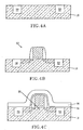
- FIGS. 6A-6B show the change of saturation current of narrow width devices.
- the nMOS current will be degraded by a large S/D overhang region and improved by a smaller S/D overhang region.
- This threshold region from mobility degradation to improvement indicates the effect from uni-axial to biaxial stress effect.
- Devices on (110) wafers have higher sensitivity than those on (110) wafers, and the improvement can be as high as 155%. This suggests that the longitudinal compressive stress plus the lateral stress, or simply biaxial compressive stress, can enhance the nMOS current.
- the nitride liner can also modulate the biaxial stress effect and is more effective on the devices built on the (110) wafer and narrow width devices ( FIGS. 7A-7B).
- FIGS. 7A-7B show the change of saturation current of narrow width devices.
- nMOS has current improvement instead of degradation with small S/D overhang region when the width is narrower than 0.2 mm.
- pMOS will have higher mobility change for narrower width devices compared to long width devices. Both uni-axial longitudinal and biaxial stress can improve pMOS performance.
Landscapes
- Insulated Gate Type Field-Effect Transistor (AREA)
- Metal-Oxide And Bipolar Metal-Oxide Semiconductor Integrated Circuits (AREA)
- Thin Film Transistor (AREA)
- Element Separation (AREA)
- Recrystallisation Techniques (AREA)
- Formation Of Insulating Films (AREA)
- Chemical Vapour Deposition (AREA)
- Luminescent Compositions (AREA)
- Photoreceptors In Electrophotography (AREA)
- Polymers With Sulfur, Phosphorus Or Metals In The Main Chain (AREA)
Claims (6)
- Matériau semi-conducteur, comprenant une couche (16) contenant du silicium, ayant une orientation de surface de cristal <110>, ladite couche contenant du silicium étant placée sous une contrainte compressive biaxiale, caractérisé en outre par le fait que la couche contenant du silicium surjacente à un substrat (20) présente un coefficient de dilatation thermique supérieur au coefficient de dilatation thermique de la couche contenant du silicium.
- Matériau semi-conducteur selon la revendication 1, dans lequel la contrainte compressive biaxiale est supérieure à 0,2 %.
- Matériau semi-conducteur selon la revendication 2, dans lequel la contrainte compressive biaxiale est supérieure à 0,3 %.
- Matériau semi-conducteur selon la revendication 1, comprenant une couche d'oxude (18), placée entre la couche contenant du silicium et le substrat.
- Matériau semi-conducteur selon la revendication 1, dans lequel le substrat est du saphir, du germanium ou du fluorure de calcium.
- Procédé de formation d'un matériau semi-conducteur contenant du silicium, comprenant les étapes consistant à :fournir une couche (16) contenant du silicium ayant une orientation de surface de cristal <110> ;lier ladite couche contenant du silicium à un substrat (20) présentant un coefficient de dilatation thermique supérieur au coefficient de dilatation thermique de ladite couche contenant du silicium ;durant la liaison, chauffer la couche contenant du silicium et le substrat à une température élevée ; etensuite, refroidir la couche contenant du silicium et le substrat liés, de manière à créer une contrainte compressive biaxiale dans ladite couche contenant du silicium.
Applications Claiming Priority (3)
| Application Number | Priority Date | Filing Date | Title |
|---|---|---|---|
| US53491604P | 2004-01-07 | 2004-01-07 | |
| US10/980,220 US7161169B2 (en) | 2004-01-07 | 2004-11-03 | Enhancement of electron and hole mobilities in <110> Si under biaxial compressive strain |
| PCT/US2004/042179 WO2006057645A2 (fr) | 2004-01-07 | 2004-12-15 | Amelioration de mobilites d'electrons et de trous en silicium 110 sous contrainte compressive biaxiale |
Publications (2)
| Publication Number | Publication Date |
|---|---|
| EP1702365A2 EP1702365A2 (fr) | 2006-09-20 |
| EP1702365B1 true EP1702365B1 (fr) | 2009-12-02 |
Family
ID=34713837
Family Applications (1)
| Application Number | Title | Priority Date | Filing Date |
|---|---|---|---|
| EP04822326A Expired - Lifetime EP1702365B1 (fr) | 2004-01-07 | 2004-12-15 | Amelioration de mobilites d'electrons et de trous en silicium 110 sous contrainte compressive biaxiale |
Country Status (8)
| Country | Link |
|---|---|
| US (5) | US7161169B2 (fr) |
| EP (1) | EP1702365B1 (fr) |
| JP (1) | JP5190201B2 (fr) |
| KR (1) | KR100961751B1 (fr) |
| AT (1) | ATE450892T1 (fr) |
| DE (1) | DE602004024448D1 (fr) |
| TW (1) | TWI430329B (fr) |
| WO (1) | WO2006057645A2 (fr) |
Families Citing this family (11)
| Publication number | Priority date | Publication date | Assignee | Title |
|---|---|---|---|---|
| US7217949B2 (en) * | 2004-07-01 | 2007-05-15 | International Business Machines Corporation | Strained Si MOSFET on tensile-strained SiGe-on-insulator (SGOI) |
| US7271043B2 (en) * | 2005-01-18 | 2007-09-18 | International Business Machines Corporation | Method for manufacturing strained silicon directly-on-insulator substrate with hybrid crystalline orientation and different stress levels |
| US8729635B2 (en) * | 2006-01-18 | 2014-05-20 | Macronix International Co., Ltd. | Semiconductor device having a high stress material layer |
| US7572712B2 (en) | 2006-11-21 | 2009-08-11 | Chartered Semiconductor Manufacturing, Ltd. | Method to form selective strained Si using lateral epitaxy |
| US7524740B1 (en) | 2008-04-24 | 2009-04-28 | International Business Machines Corporation | Localized strain relaxation for strained Si directly on insulator |
| JP4875115B2 (ja) * | 2009-03-05 | 2012-02-15 | 株式会社東芝 | 半導体素子及び半導体装置 |
| FR2966285B1 (fr) | 2010-10-14 | 2013-09-06 | St Microelectronics Crolles 2 | Procédé de formation de circuits intégrés sur substrat semi conducteur contraint |
| CN103270378B (zh) * | 2010-12-22 | 2016-01-27 | 国际商业机器公司 | 固体吸附制冷 |
| US8972053B2 (en) | 2011-08-30 | 2015-03-03 | 5D Robotics, Inc. | Universal payload abstraction |
| US8895381B1 (en) * | 2013-08-15 | 2014-11-25 | International Business Machines Corporation | Method of co-integration of strained-Si and relaxed Si or strained SiGe FETs on insulator with planar and non-planar architectures |
| CN110838435B (zh) * | 2019-10-14 | 2023-01-31 | 宁波大学 | 一种外延层转移方法 |
Family Cites Families (20)
| Publication number | Priority date | Publication date | Assignee | Title |
|---|---|---|---|---|
| JPS5317069A (en) * | 1976-07-30 | 1978-02-16 | Fujitsu Ltd | Semiconductor device and its production |
| JPH10107380A (ja) * | 1996-09-30 | 1998-04-24 | Toshiba Corp | 積層体のへき開方法 |
| JP3676910B2 (ja) * | 1997-07-30 | 2005-07-27 | インターナショナル・ビジネス・マシーンズ・コーポレーション | 半導体装置及び半導体アイランドの形成方法 |
| US20010020723A1 (en) * | 1998-07-07 | 2001-09-13 | Mark I. Gardner | Transistor having a transition metal oxide gate dielectric and method of making same |
| JP4476390B2 (ja) * | 1998-09-04 | 2010-06-09 | 株式会社半導体エネルギー研究所 | 半導体装置の作製方法 |
| JP4521542B2 (ja) * | 1999-03-30 | 2010-08-11 | ルネサスエレクトロニクス株式会社 | 半導体装置および半導体基板 |
| CN101465295A (zh) * | 2000-11-22 | 2009-06-24 | 株式会社日立制作所 | 半导体器件及其制造方法 |
| US6686300B2 (en) * | 2000-12-27 | 2004-02-03 | Texas Instruments Incorporated | Sub-critical-dimension integrated circuit features |
| US6531739B2 (en) * | 2001-04-05 | 2003-03-11 | Peregrine Semiconductor Corporation | Radiation-hardened silicon-on-insulator CMOS device, and method of making the same |
| JP2003017668A (ja) * | 2001-06-29 | 2003-01-17 | Canon Inc | 部材の分離方法及び分離装置 |
| JP3782021B2 (ja) * | 2002-02-22 | 2006-06-07 | 株式会社東芝 | 半導体装置、半導体装置の製造方法、半導体基板の製造方法 |
| WO2003105189A2 (fr) * | 2002-06-07 | 2003-12-18 | Amberwave Systems Corporation | Structures de dispositif a semi-conducteurs contraints sur isolant |
| US20030227057A1 (en) * | 2002-06-07 | 2003-12-11 | Lochtefeld Anthony J. | Strained-semiconductor-on-insulator device structures |
| TWI242796B (en) * | 2002-09-04 | 2005-11-01 | Canon Kk | Substrate and manufacturing method therefor |
| AU2003264642B2 (en) * | 2002-12-02 | 2009-08-06 | Tadahiro Ohmi | Semiconductor Device and Method of Manufacturing the Same |
| US7115480B2 (en) * | 2003-05-07 | 2006-10-03 | Micron Technology, Inc. | Micromechanical strained semiconductor by wafer bonding |
| US20040222090A1 (en) * | 2003-05-07 | 2004-11-11 | Tim Scott | Carbon fiber and copper support for physical vapor deposition target assemblies |
| FR2859312B1 (fr) * | 2003-09-02 | 2006-02-17 | Soitec Silicon On Insulator | Scellement metallique multifonction |
| US7354815B2 (en) * | 2003-11-18 | 2008-04-08 | Silicon Genesis Corporation | Method for fabricating semiconductor devices using strained silicon bearing material |
| JP4349151B2 (ja) * | 2004-02-26 | 2009-10-21 | トヨタ自動車株式会社 | 接触状態取得装置 |
-
2004
- 2004-11-03 US US10/980,220 patent/US7161169B2/en not_active Expired - Fee Related
- 2004-12-15 AT AT04822326T patent/ATE450892T1/de not_active IP Right Cessation
- 2004-12-15 WO PCT/US2004/042179 patent/WO2006057645A2/fr not_active Ceased
- 2004-12-15 KR KR1020067013491A patent/KR100961751B1/ko not_active Expired - Fee Related
- 2004-12-15 EP EP04822326A patent/EP1702365B1/fr not_active Expired - Lifetime
- 2004-12-15 DE DE602004024448T patent/DE602004024448D1/de not_active Expired - Lifetime
- 2004-12-15 JP JP2006549292A patent/JP5190201B2/ja not_active Expired - Fee Related
-
2005
- 2005-01-03 TW TW094100053A patent/TWI430329B/zh not_active IP Right Cessation
-
2006
- 2006-12-18 US US11/612,309 patent/US7314790B2/en not_active Expired - Fee Related
-
2007
- 2007-10-25 US US11/924,015 patent/US20080044987A1/en not_active Abandoned
- 2007-10-25 US US11/924,024 patent/US7462525B2/en not_active Expired - Lifetime
-
2008
- 2008-05-06 US US12/115,731 patent/US7943486B2/en not_active Expired - Fee Related
Non-Patent Citations (2)
| Title |
|---|
| JOURNAL ARTICLE: "Applying mechanical stress to improve MOS semiconductor performance", IBM TECHNICAL DISCLOSURE BULLETIN, vol. 30, no. 9, 1 February 1988 (1988-02-01), IBM CORP. NEW YORK, US, pages 330 - 333, XP000104874 * |
| MIZUNO T. ET AL: "(110)-Surface Strained-SOI CMOS Device with Higher Carrier Mobility", 2003 SYMPOSIUM ON VLSI TECHNOLOGY. DIGEST OF TECHNICAL PAPERS, 10 June 2003 (2003-06-10), NEW YORK, NY : IEEE, US, pages 97 - 98, XP001211708 * |
Also Published As
| Publication number | Publication date |
|---|---|
| WO2006057645A2 (fr) | 2006-06-01 |
| KR20060127021A (ko) | 2006-12-11 |
| JP2007527113A (ja) | 2007-09-20 |
| EP1702365A2 (fr) | 2006-09-20 |
| US7161169B2 (en) | 2007-01-09 |
| US20080044987A1 (en) | 2008-02-21 |
| US20050145837A1 (en) | 2005-07-07 |
| WO2006057645A3 (fr) | 2006-11-30 |
| WO2006057645A8 (fr) | 2006-08-03 |
| US20070099367A1 (en) | 2007-05-03 |
| US20080044966A1 (en) | 2008-02-21 |
| US20080206958A1 (en) | 2008-08-28 |
| DE602004024448D1 (de) | 2010-01-14 |
| JP5190201B2 (ja) | 2013-04-24 |
| KR100961751B1 (ko) | 2010-06-07 |
| US7462525B2 (en) | 2008-12-09 |
| ATE450892T1 (de) | 2009-12-15 |
| WO2006057645A9 (fr) | 2006-09-14 |
| TW200616021A (en) | 2006-05-16 |
| US7943486B2 (en) | 2011-05-17 |
| TWI430329B (zh) | 2014-03-11 |
| US7314790B2 (en) | 2008-01-01 |
Similar Documents
| Publication | Publication Date | Title |
|---|---|---|
| US7943486B2 (en) | Enhancement of electron and hole mobilities in <110> Si under biaxial compressive strain | |
| CA2501580C (fr) | Procede de formation de silicium contraint sur un isolant (ssoi), et structures formees y relatives | |
| US8017499B2 (en) | Strained Si MOSFET on tensile-strained SiGe-on-insulator (SGOI) | |
| US6583015B2 (en) | Gate technology for strained surface channel and strained buried channel MOSFET devices | |
| JP2008504678A (ja) | 圧縮歪Ge層内にPMOSデバイスを作製する構造および方法(先端CMOS技術への歪Geの統合) | |
| JP2009105427A (ja) | 半導体基板の製造方法 | |
| US20050280026A1 (en) | Strained silicon-on-silicon by wafer bonding and layer transfer | |
| WO2006002410A2 (fr) | Croissance de sige <110> par compression et structure de dispositif de transistor a effet de champ a porte isolee | |
| WO2005122272A1 (fr) | Transistor a effet de champ 'mis' ayant une couche de canal de silicium sous contrainte | |
| US20050285140A1 (en) | Isolation structure for strained channel transistors | |
| CN100544022C (zh) | 具有<110>晶体取向含硅层的半导体材料及其形成方法 | |
| US20050070070A1 (en) | Method of forming strained silicon on insulator | |
| US20070010070A1 (en) | Fabrication of strained semiconductor-on-insulator (ssoi) structures by using strained insulating layers | |
| JP2004356644A (ja) | 半導体基板の製造方法 |
Legal Events
| Date | Code | Title | Description |
|---|---|---|---|
| PUAI | Public reference made under article 153(3) epc to a published international application that has entered the european phase |
Free format text: ORIGINAL CODE: 0009012 |
|
| 17P | Request for examination filed |
Effective date: 20060622 |
|
| AK | Designated contracting states |
Kind code of ref document: A2 Designated state(s): AT BE BG CH CY CZ DE DK EE ES FI FR GB GR HU IE IS IT LI LT LU MC NL PL PT RO SE SI SK TR |
|
| AX | Request for extension of the european patent |
Extension state: AL BA HR LV MK YU |
|
| PUAK | Availability of information related to the publication of the international search report |
Free format text: ORIGINAL CODE: 0009015 |
|
| R17D | Deferred search report published (corrected) |
Effective date: 20061130 |
|
| RIN1 | Information on inventor provided before grant (corrected) |
Inventor name: HERGENROTHER, JOHN, M. Inventor name: SOLOMON, PAUL Inventor name: LEONG, MEIKEI Inventor name: CHAN, VICTOR Inventor name: RENGARAJAN, RAJESH Inventor name: REZNICEK, ALEXANDER C/O IBM UNITED KINGDOM LTD Inventor name: FISCHETTI, MASSIMO, V. Inventor name: SUNG, CHUN-YUNG Inventor name: YANG, MIN |
|
| 17Q | First examination report despatched |
Effective date: 20070201 |
|
| DAX | Request for extension of the european patent (deleted) | ||
| GRAP | Despatch of communication of intention to grant a patent |
Free format text: ORIGINAL CODE: EPIDOSNIGR1 |
|
| GRAS | Grant fee paid |
Free format text: ORIGINAL CODE: EPIDOSNIGR3 |
|
| GRAA | (expected) grant |
Free format text: ORIGINAL CODE: 0009210 |
|
| AK | Designated contracting states |
Kind code of ref document: B1 Designated state(s): AT BE BG CH CY CZ DE DK EE ES FI FR GB GR HU IE IS IT LI LT LU MC NL PL PT RO SE SI SK TR |
|
| REG | Reference to a national code |
Ref country code: GB Ref legal event code: FG4D |
|
| REG | Reference to a national code |
Ref country code: CH Ref legal event code: EP Ref country code: CH Ref legal event code: NV Representative=s name: IBM RESEARCH GMBH ZURICH RESEARCH LABORATORY INTEL |
|
| REG | Reference to a national code |
Ref country code: IE Ref legal event code: FG4D |
|
| REG | Reference to a national code |
Ref country code: GB Ref legal event code: 746 Effective date: 20091221 |
|
| REF | Corresponds to: |
Ref document number: 602004024448 Country of ref document: DE Date of ref document: 20100114 Kind code of ref document: P |
|
| REG | Reference to a national code |
Ref country code: NL Ref legal event code: VDEP Effective date: 20091202 |
|
| PG25 | Lapsed in a contracting state [announced via postgrant information from national office to epo] |
Ref country code: LT Free format text: LAPSE BECAUSE OF FAILURE TO SUBMIT A TRANSLATION OF THE DESCRIPTION OR TO PAY THE FEE WITHIN THE PRESCRIBED TIME-LIMIT Effective date: 20091202 Ref country code: SE Free format text: LAPSE BECAUSE OF FAILURE TO SUBMIT A TRANSLATION OF THE DESCRIPTION OR TO PAY THE FEE WITHIN THE PRESCRIBED TIME-LIMIT Effective date: 20091202 Ref country code: FI Free format text: LAPSE BECAUSE OF FAILURE TO SUBMIT A TRANSLATION OF THE DESCRIPTION OR TO PAY THE FEE WITHIN THE PRESCRIBED TIME-LIMIT Effective date: 20091202 |
|
| LTIE | Lt: invalidation of european patent or patent extension |
Effective date: 20091202 |
|
| PG25 | Lapsed in a contracting state [announced via postgrant information from national office to epo] |
Ref country code: CY Free format text: LAPSE BECAUSE OF FAILURE TO SUBMIT A TRANSLATION OF THE DESCRIPTION OR TO PAY THE FEE WITHIN THE PRESCRIBED TIME-LIMIT Effective date: 20091202 Ref country code: SI Free format text: LAPSE BECAUSE OF FAILURE TO SUBMIT A TRANSLATION OF THE DESCRIPTION OR TO PAY THE FEE WITHIN THE PRESCRIBED TIME-LIMIT Effective date: 20091202 Ref country code: PL Free format text: LAPSE BECAUSE OF FAILURE TO SUBMIT A TRANSLATION OF THE DESCRIPTION OR TO PAY THE FEE WITHIN THE PRESCRIBED TIME-LIMIT Effective date: 20091202 |
|
| PG25 | Lapsed in a contracting state [announced via postgrant information from national office to epo] |
Ref country code: AT Free format text: LAPSE BECAUSE OF FAILURE TO SUBMIT A TRANSLATION OF THE DESCRIPTION OR TO PAY THE FEE WITHIN THE PRESCRIBED TIME-LIMIT Effective date: 20091202 |
|
| PG25 | Lapsed in a contracting state [announced via postgrant information from national office to epo] |
Ref country code: RO Free format text: LAPSE BECAUSE OF FAILURE TO SUBMIT A TRANSLATION OF THE DESCRIPTION OR TO PAY THE FEE WITHIN THE PRESCRIBED TIME-LIMIT Effective date: 20091202 Ref country code: PT Free format text: LAPSE BECAUSE OF FAILURE TO SUBMIT A TRANSLATION OF THE DESCRIPTION OR TO PAY THE FEE WITHIN THE PRESCRIBED TIME-LIMIT Effective date: 20100402 Ref country code: ES Free format text: LAPSE BECAUSE OF FAILURE TO SUBMIT A TRANSLATION OF THE DESCRIPTION OR TO PAY THE FEE WITHIN THE PRESCRIBED TIME-LIMIT Effective date: 20100313 Ref country code: BG Free format text: LAPSE BECAUSE OF FAILURE TO SUBMIT A TRANSLATION OF THE DESCRIPTION OR TO PAY THE FEE WITHIN THE PRESCRIBED TIME-LIMIT Effective date: 20100302 Ref country code: EE Free format text: LAPSE BECAUSE OF FAILURE TO SUBMIT A TRANSLATION OF THE DESCRIPTION OR TO PAY THE FEE WITHIN THE PRESCRIBED TIME-LIMIT Effective date: 20091202 Ref country code: NL Free format text: LAPSE BECAUSE OF FAILURE TO SUBMIT A TRANSLATION OF THE DESCRIPTION OR TO PAY THE FEE WITHIN THE PRESCRIBED TIME-LIMIT Effective date: 20091202 Ref country code: MC Free format text: LAPSE BECAUSE OF NON-PAYMENT OF DUE FEES Effective date: 20100701 Ref country code: IS Free format text: LAPSE BECAUSE OF FAILURE TO SUBMIT A TRANSLATION OF THE DESCRIPTION OR TO PAY THE FEE WITHIN THE PRESCRIBED TIME-LIMIT Effective date: 20100402 |
|
| REG | Reference to a national code |
Ref country code: CH Ref legal event code: PL |
|
| PG25 | Lapsed in a contracting state [announced via postgrant information from national office to epo] |
Ref country code: BE Free format text: LAPSE BECAUSE OF FAILURE TO SUBMIT A TRANSLATION OF THE DESCRIPTION OR TO PAY THE FEE WITHIN THE PRESCRIBED TIME-LIMIT Effective date: 20091202 Ref country code: CZ Free format text: LAPSE BECAUSE OF FAILURE TO SUBMIT A TRANSLATION OF THE DESCRIPTION OR TO PAY THE FEE WITHIN THE PRESCRIBED TIME-LIMIT Effective date: 20091202 Ref country code: SK Free format text: LAPSE BECAUSE OF FAILURE TO SUBMIT A TRANSLATION OF THE DESCRIPTION OR TO PAY THE FEE WITHIN THE PRESCRIBED TIME-LIMIT Effective date: 20091202 |
|
| PLBE | No opposition filed within time limit |
Free format text: ORIGINAL CODE: 0009261 |
|
| STAA | Information on the status of an ep patent application or granted ep patent |
Free format text: STATUS: NO OPPOSITION FILED WITHIN TIME LIMIT |
|
| PG25 | Lapsed in a contracting state [announced via postgrant information from national office to epo] |
Ref country code: IE Free format text: LAPSE BECAUSE OF NON-PAYMENT OF DUE FEES Effective date: 20091215 Ref country code: LI Free format text: LAPSE BECAUSE OF NON-PAYMENT OF DUE FEES Effective date: 20091231 Ref country code: CH Free format text: LAPSE BECAUSE OF NON-PAYMENT OF DUE FEES Effective date: 20091231 Ref country code: GR Free format text: LAPSE BECAUSE OF FAILURE TO SUBMIT A TRANSLATION OF THE DESCRIPTION OR TO PAY THE FEE WITHIN THE PRESCRIBED TIME-LIMIT Effective date: 20100303 |
|
| 26N | No opposition filed |
Effective date: 20100903 |
|
| PG25 | Lapsed in a contracting state [announced via postgrant information from national office to epo] |
Ref country code: DK Free format text: LAPSE BECAUSE OF FAILURE TO SUBMIT A TRANSLATION OF THE DESCRIPTION OR TO PAY THE FEE WITHIN THE PRESCRIBED TIME-LIMIT Effective date: 20091202 |
|
| PG25 | Lapsed in a contracting state [announced via postgrant information from national office to epo] |
Ref country code: IT Free format text: LAPSE BECAUSE OF FAILURE TO SUBMIT A TRANSLATION OF THE DESCRIPTION OR TO PAY THE FEE WITHIN THE PRESCRIBED TIME-LIMIT Effective date: 20091202 |
|
| PG25 | Lapsed in a contracting state [announced via postgrant information from national office to epo] |
Ref country code: LU Free format text: LAPSE BECAUSE OF NON-PAYMENT OF DUE FEES Effective date: 20091215 |
|
| PG25 | Lapsed in a contracting state [announced via postgrant information from national office to epo] |
Ref country code: HU Free format text: LAPSE BECAUSE OF FAILURE TO SUBMIT A TRANSLATION OF THE DESCRIPTION OR TO PAY THE FEE WITHIN THE PRESCRIBED TIME-LIMIT Effective date: 20100603 |
|
| PG25 | Lapsed in a contracting state [announced via postgrant information from national office to epo] |
Ref country code: TR Free format text: LAPSE BECAUSE OF FAILURE TO SUBMIT A TRANSLATION OF THE DESCRIPTION OR TO PAY THE FEE WITHIN THE PRESCRIBED TIME-LIMIT Effective date: 20091202 |
|
| REG | Reference to a national code |
Ref country code: FR Ref legal event code: PLFP Year of fee payment: 12 |
|
| PGFP | Annual fee paid to national office [announced via postgrant information from national office to epo] |
Ref country code: GB Payment date: 20151209 Year of fee payment: 12 |
|
| REG | Reference to a national code |
Ref country code: DE Ref legal event code: R081 Ref document number: 602004024448 Country of ref document: DE Owner name: GLOBALFOUNDRIES INC., KY Free format text: FORMER OWNER: INTERNATIONAL BUSINESS MACHINES CORPORATION, ARMONK, NY, US Ref country code: DE Ref legal event code: R082 Ref document number: 602004024448 Country of ref document: DE Representative=s name: RICHARDT PATENTANWAELTE PARTG MBB, DE Ref country code: DE Ref legal event code: R081 Ref document number: 602004024448 Country of ref document: DE Owner name: GLOBALFOUNDRIES INC., KY Free format text: FORMER OWNER: INTERNATIONAL BUSINESS MACHINES CORPORATION, ARMONK, N.Y., US |
|
| REG | Reference to a national code |
Ref country code: DE Ref legal event code: R082 Ref document number: 602004024448 Country of ref document: DE Representative=s name: RICHARDT PATENTANWAELTE PARTG MBB, DE Ref country code: DE Ref legal event code: R081 Ref document number: 602004024448 Country of ref document: DE Owner name: GLOBALFOUNDRIES INC., KY Free format text: FORMER OWNER: GLOBALFOUNDRIES US 2 LLC (N.D.GES.DES STAATES DELAWARE), HOPEWELL JUNCTION, N.Y., US |
|
| REG | Reference to a national code |
Ref country code: FR Ref legal event code: TP Owner name: GLOBALFOUNDRIES INC., GB Effective date: 20160829 |
|
| REG | Reference to a national code |
Ref country code: FR Ref legal event code: PLFP Year of fee payment: 13 |
|
| PGFP | Annual fee paid to national office [announced via postgrant information from national office to epo] |
Ref country code: FR Payment date: 20161111 Year of fee payment: 13 |
|
| GBPC | Gb: european patent ceased through non-payment of renewal fee |
Effective date: 20161215 |
|
| PG25 | Lapsed in a contracting state [announced via postgrant information from national office to epo] |
Ref country code: GB Free format text: LAPSE BECAUSE OF NON-PAYMENT OF DUE FEES Effective date: 20161215 |
|
| PGFP | Annual fee paid to national office [announced via postgrant information from national office to epo] |
Ref country code: DE Payment date: 20171212 Year of fee payment: 14 |
|
| REG | Reference to a national code |
Ref country code: FR Ref legal event code: ST Effective date: 20180831 |
|
| PG25 | Lapsed in a contracting state [announced via postgrant information from national office to epo] |
Ref country code: FR Free format text: LAPSE BECAUSE OF NON-PAYMENT OF DUE FEES Effective date: 20180102 |
|
| REG | Reference to a national code |
Ref country code: DE Ref legal event code: R119 Ref document number: 602004024448 Country of ref document: DE |
|
| PG25 | Lapsed in a contracting state [announced via postgrant information from national office to epo] |
Ref country code: DE Free format text: LAPSE BECAUSE OF NON-PAYMENT OF DUE FEES Effective date: 20190702 |