EP1672712A2 - Méthode de fabrication des réseaux d'éléments à couche épaisse céramique ayant petites largeurs de trait, definitions de haute précision, et/ou hauts facteurs d'aspect - Google Patents
Méthode de fabrication des réseaux d'éléments à couche épaisse céramique ayant petites largeurs de trait, definitions de haute précision, et/ou hauts facteurs d'aspect Download PDFInfo
- Publication number
- EP1672712A2 EP1672712A2 EP05112474A EP05112474A EP1672712A2 EP 1672712 A2 EP1672712 A2 EP 1672712A2 EP 05112474 A EP05112474 A EP 05112474A EP 05112474 A EP05112474 A EP 05112474A EP 1672712 A2 EP1672712 A2 EP 1672712A2
- Authority
- EP
- European Patent Office
- Prior art keywords
- mold
- elements
- depositing
- piezoelectric
- ceramic material
- Prior art date
- Legal status (The legal status is an assumption and is not a legal conclusion. Google has not performed a legal analysis and makes no representation as to the accuracy of the status listed.)
- Granted
Links
Images


Classifications
-
- H—ELECTRICITY
- H10—SEMICONDUCTOR DEVICES; ELECTRIC SOLID-STATE DEVICES NOT OTHERWISE PROVIDED FOR
- H10N—ELECTRIC SOLID-STATE DEVICES NOT OTHERWISE PROVIDED FOR
- H10N39/00—Integrated devices, or assemblies of multiple devices, comprising at least one piezoelectric, electrostrictive or magnetostrictive element covered by groups H10N30/00 – H10N35/00
-
- H—ELECTRICITY
- H10—SEMICONDUCTOR DEVICES; ELECTRIC SOLID-STATE DEVICES NOT OTHERWISE PROVIDED FOR
- H10N—ELECTRIC SOLID-STATE DEVICES NOT OTHERWISE PROVIDED FOR
- H10N30/00—Piezoelectric or electrostrictive devices
- H10N30/01—Manufacture or treatment
- H10N30/07—Forming of piezoelectric or electrostrictive parts or bodies on an electrical element or another base
- H10N30/072—Forming of piezoelectric or electrostrictive parts or bodies on an electrical element or another base by laminating or bonding of piezoelectric or electrostrictive bodies
- H10N30/073—Forming of piezoelectric or electrostrictive parts or bodies on an electrical element or another base by laminating or bonding of piezoelectric or electrostrictive bodies by fusion of metals or by adhesives
-
- H—ELECTRICITY
- H10—SEMICONDUCTOR DEVICES; ELECTRIC SOLID-STATE DEVICES NOT OTHERWISE PROVIDED FOR
- H10N—ELECTRIC SOLID-STATE DEVICES NOT OTHERWISE PROVIDED FOR
- H10N30/00—Piezoelectric or electrostrictive devices
- H10N30/01—Manufacture or treatment
- H10N30/08—Shaping or machining of piezoelectric or electrostrictive bodies
- H10N30/081—Shaping or machining of piezoelectric or electrostrictive bodies by coating or depositing using masks, e.g. lift-off
-
- H—ELECTRICITY
- H10—SEMICONDUCTOR DEVICES; ELECTRIC SOLID-STATE DEVICES NOT OTHERWISE PROVIDED FOR
- H10N—ELECTRIC SOLID-STATE DEVICES NOT OTHERWISE PROVIDED FOR
- H10N30/00—Piezoelectric or electrostrictive devices
- H10N30/80—Constructional details
- H10N30/85—Piezoelectric or electrostrictive active materials
- H10N30/853—Ceramic compositions
- H10N30/8548—Lead based oxides
- H10N30/8554—Lead zirconium titanate based
-
- Y—GENERAL TAGGING OF NEW TECHNOLOGICAL DEVELOPMENTS; GENERAL TAGGING OF CROSS-SECTIONAL TECHNOLOGIES SPANNING OVER SEVERAL SECTIONS OF THE IPC; TECHNICAL SUBJECTS COVERED BY FORMER USPC CROSS-REFERENCE ART COLLECTIONS [XRACs] AND DIGESTS
- Y10—TECHNICAL SUBJECTS COVERED BY FORMER USPC
- Y10T—TECHNICAL SUBJECTS COVERED BY FORMER US CLASSIFICATION
- Y10T29/00—Metal working
- Y10T29/42—Piezoelectric device making
-
- Y—GENERAL TAGGING OF NEW TECHNOLOGICAL DEVELOPMENTS; GENERAL TAGGING OF CROSS-SECTIONAL TECHNOLOGIES SPANNING OVER SEVERAL SECTIONS OF THE IPC; TECHNICAL SUBJECTS COVERED BY FORMER USPC CROSS-REFERENCE ART COLLECTIONS [XRACs] AND DIGESTS
- Y10—TECHNICAL SUBJECTS COVERED BY FORMER USPC
- Y10T—TECHNICAL SUBJECTS COVERED BY FORMER US CLASSIFICATION
- Y10T29/00—Metal working
- Y10T29/43—Electric condenser making
- Y10T29/435—Solid dielectric type
-
- Y—GENERAL TAGGING OF NEW TECHNOLOGICAL DEVELOPMENTS; GENERAL TAGGING OF CROSS-SECTIONAL TECHNOLOGIES SPANNING OVER SEVERAL SECTIONS OF THE IPC; TECHNICAL SUBJECTS COVERED BY FORMER USPC CROSS-REFERENCE ART COLLECTIONS [XRACs] AND DIGESTS
- Y10—TECHNICAL SUBJECTS COVERED BY FORMER USPC
- Y10T—TECHNICAL SUBJECTS COVERED BY FORMER US CLASSIFICATION
- Y10T29/00—Metal working
- Y10T29/49—Method of mechanical manufacture
- Y10T29/49002—Electrical device making
- Y10T29/49117—Conductor or circuit manufacturing
- Y10T29/49124—On flat or curved insulated base, e.g., printed circuit, etc.
- Y10T29/49155—Manufacturing circuit on or in base
- Y10T29/49163—Manufacturing circuit on or in base with sintering of base
Definitions
- the present exemplary embodiments relate to a method for forming ceramic (e.g., piezoelectric such as lead zirconate titanate (PZT)) thick film element arrays with fine feature size, high-precision definition, and/or high aspect ratios. It finds particular application in conjunction with high frequency and/or ultrasonic implementations, and will be described with particular reference thereto. However, it is to be appreciated that the present exemplary embodiment is also amenable to other like applications.
- ceramic e.g., piezoelectric such as lead zirconate titanate (PZT)
- PZT lead zirconate titanate
- Ceramic thick films especially piezoelectric thick film (thickness between 10 to 100 ⁇ m) element arrays with fine feature size, high-precision definition, and/or high aspect ratios have many applications in, for example, micro electromechanical systems (MEMS) devices, nondestructive testing and medical imaging.
- MEMS micro electromechanical systems
- a one-dimensional (1-D) piezoelectric element array 10 for medical ultrasound imaging may comprise a plurality of high-aspect elements 12.
- the thickness t of the piezoelectric elements should be approximately ⁇ PZT /2, where ⁇ PZT is the acoustic wavelength in PZT ceramics.
- ⁇ PZT is the acoustic wavelength in PZT ceramics.
- the thickness of the PZT elements should be approximately 50 ⁇ m.
- the center-to-center distance d of the PZT elements should be about half of the acoustic wavelength in human organs, which is close to that of water.
- the lateral dimension b of the PZT elements being approximately ⁇ water /3.
- the lateral dimension b should be about 12.5 ⁇ m, and the spacing between the elements should be about 6.25 ⁇ m.
- sol-gel derived PZT films Due to the limited doping effect in the sol-gel films, the properties of the sol-gel derived PZT films cannot be easily tailored. That is, it is very difficult to make sol-gel PZT films to be intentionally soft or hard. Third, the sol-gel derived PZT films need to be annealed at 600°C or higher, so the choice of the substrates is limited.
- a method comprises depositing ceramic material into a mold disposed on a temporary substrate, removing the mold to obtain molded elements comprising the material, sintering the molded elements, bonding the molded elements to a target substrate and removing the temporary substrate.
- the method further comprises forming the mold of SU-8 or other suitable photoresist material.
- the method further comprises depositing electrodes on the molded elements;
- depositing the ceramic material comprises screen printing ceramic material into recesses of the mold.
- depositing the ceramic material comprises depositing a paste of ceramic material into the mold by a casting or a wiping process.
- the depositing of the ceramic material comprises use of an electrophoretic or gravity technique.
- removing of the mold comprises removing the mold by laser ablation through a mask.
- the removing of the mold comprises exposing the mold to a relatively high temperature in an open environment.
- the sintering is performed in a controlled environment having, for example, a lead-rich atmosphere.
- the sintering is performed at 600°C to 1500°C, and more preferably, at 1100°C to 1350°C.
- the ceramic material is prepared as a paste.
- the ceramic material is lead zirconate titanate (PZT) material.
- the temporary substrate is sapphire, zirconia, strontium titanate, or other suitable materials.
- the sintering is performed at 1100°C to 1350°C.
- the sintering is performed in a controlled environment.
- the controlled environment is a lead-rich atmosphere.
- the temporary substrate is sapphire or other suitable refractory material.
- the removing of temporary substrate comprises use of laser liftoff technique wherein the ceramic material is exposed to an excimer laser source through the temporary substrate.
- a method comprises forming a mold on a temporary substrate, depositing piezoelectric material into the mold, removing the mold to obtain molded piezoelectric elements comprising the piezoelectric material, sintering the piezoelectric elements, depositing first electrodes on the piezoelectric elements, bonding the piezoelectric elements to a target substrate, removing the temporary substrate and depositing second electrodes on the piezoelectric elements.
- the mold is formed of SU-8 or other suitable photoresist material.
- depositing the piezoelectric material comprises screen printing the piezoelectric material into recesses of the mold followed by a drying or soft baking process.
- the depositing of the piezoelectric material comprises depositing a paste of the piezoelectric material into the mold by a casting or a wiping process, followed by a drying or soft baking process.
- the removing of the mold comprises removing the mold by laser ablation through a mask.
- the removing of the mold comprises exposing the mold to a relatively high temperature in an open environment.
- the sintering is performed in a controlled environment in a lead-rich atmosphere.
- the sintering is performed at 600°C to 1500°C, and more preferably at 1100°C to 1350°C.
- the piezoelectric material is prepared as a paste.
- the piezoelectric material is lead zirconate titanate (PZT) material.
- the temporary substrate is sapphire, zirconia, strontium titanate, or other suitable materials.
- the depositing of the ceramic material comprises use of an electrophoretic or gravity technique.
- laser lift-off techniques are used to remove the temporary substrate.
- soft-polishing techniques are implemented after drying or soft baking.
- FIGURE 1 is an illustration of an array of high aspect ratio elements
- FIGURE 2 is a flow chart illustrating an overall method of the presently described embodiments
- FIGURE 3 is an illustration of a portion of a method according to the presently described embodiments.
- FIGURE 4 is an illustration of a portion of a method according to the presently described embodiments.
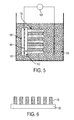
- FIGURE 5 is an illustration of an alternative approach to the portion of the method of FIGURE 4 portion
- FIGURE 6 is an illustration of a portion of a method according to the presently described embodiments.
- FIGURE 7 is an illustration of a portion of a method according to the presently described embodiments.
- FIGURE 8 is an illustration of a portion of a method according to the presently described embodiments.
- FIGURE 9 is an illustration of a portion of a method according to the presently described embodiments.
- techniques of screen printing or other deposition methods, molding, and laser liftoff are combined to advantageously form piezoelectric thick film elements with fine feature size, high-precision definition, and/or high aspect ratios.
- the overall method may be implemented in a number of different manners or embodiments using a variety of fabrication, hardware and/or software techniques.
- the techniques described may also vary as a function of whether the manufactured products are produced at high speed, in mass, or are custom formed.
- the method includes providing a mold on a temporary substrate, e.g., a sapphire substrate or substrate of another refractory material (at 102).
- a temporary substrate e.g., a sapphire substrate or substrate of another refractory material (at 102).
- An illustrative process for doing so will be described below; however, any of a variety of methods of mold forming may be used.
- SU-8 material is used to form the mold.
- Other photoresist material may also be used.
- a material such as PZT paste or other ceramic material is deposited into the mold (e.g., the recesses of the mold) which is disposed on the temporary substrate (at 104), followed by a drying or soft baking process if necessary.
- the mold is removed to obtain elements formed by the molds (at 106).
- these elements will then be heated to certain temperatures in an oxidizing environment (of which air is sufficiently oxidizing) to burn out the mold.
- the mold can also be removed by using laser ablation or other dry methods. Laser ablation may be conducted through a mask, if necessary.
- the formed elements will be sintered at high temperatures and, in one form, in a controlled environment with Pb-rich atmosphere (at 108). After sintering, electrode deposition is optionally performed on the elements (at 110).
- the sintered elements are then bonded to a final target substrate (at 112) and released from the temporary substrate through, for example, laser liftoff (at 114). Further, electrodes may also be optionally deposited at this point (at 116).
- the presently described embodiments combine screen printing or other deposition methods, molding such as SU-8 molding, and laser liftoff to form piezoelectric elements with fine feature size (e.g., as small as several ⁇ m in scale), high precision definition (e.g., having very sharp edges), and/or a high aspect ratio (e.g., having a thickness to width ratio larger than 2:1, and more preferably, larger than 4:1).
- the presently described embodiments as implemented may result in elements having lateral dimensions of 5 micrometers ( ⁇ m) to 5 millimeters (mm), height or thickness of 10 micrometers ( ⁇ m) to 500 micrometers ( ⁇ m), and spacing between elements of 1 micrometer ( ⁇ m) to 100 micrometers ( ⁇ m).
- One illustrative technique according to the presently described embodiments reflecting the method described in connection with Figure 2 is shown in more detail in Figures 3-9.
- a mold 150 is made on a substrate 152.
- the mold is formed (e.g., screen printed, spun, etc. to obtain uniform thickness) from SU-8 material
- the substrate is, in one form, formed from material that can withstand high temperatures such as sapphire.
- the mold 150 can be formed with a height-to-width ratio up to twenty (20), a very sharp edge, and an opening of only a few ⁇ m. It is expected that this method will allow making PZT element arrays with higher than 4:1 aspect ratio, high precision definition on the edge, and feature size at the ⁇ m scale. Of course, the dimensions and shapes may be varied. This variance between elements may even be present within a single array.
- the material of both the mold and substrate may be changed as a function of the design objectives and the implementation.
- other transparent materials such as transparent alumina ceramic, yttria-stabilized zirconia, strontium titanate, may be used for the substrate, for example, where laser lift-off is used.
- a material such as piezoelectric material 154 is deposited into the mold.
- the selected material may be lead zirconate titanate (PZT) and may take the form of paste, although other compositions and consistencies may be used.
- PZT lead zirconate titanate
- One method to deposit the material is to screen print the paste into the mold using a screen 156. Multiple passes of the screen printing mechanism may be used to deposit multiple layers of material. It should be understood that if the mold is only used to improve the edge definition of the PZT elements, i.e., the aspect ratio is not high, a slurry of material such as PZT paste can be printed into the openings of the mold using conventional screen printing methods. The air in the openings can be easily removed in this case. However, if the aspect ratio is high, other techniques for depositing may be more efficient.
- the screen printing of PZT paste may be accomplished in a vacuum.
- the rheologic properties of the paste and solvent concentration will not change significantly in this environment.
- a slurry of material such as PZT paste can also be deposited into the mold by a casting or wiping process.
- the screen 156 would not be necessary in this case. This may also be accomplished in a vacuum.
- Soft baking or drying should follow these deposition steps. Using any of these techniques (including screen printing), soft polishing may be used to level the surface. As with screen printing, multiple iterations may be used to deposit the material. So, a cycle of casting or wiping and/or soft baking or drying may be used to achieve a desired thickness of deposit. Of course, other techniques may also be implemented.
- Another method for depositing material such as PZT material into a deep hole is to use an electrophoretic method.
- the powder such as PZT powder is prepared as a colloidal dispersion by using a method such as spray coating of a binder and charge control agent and using typical colloidal dispersion preparation techniques (e.g., Isopar - like liquid toner).
- typical colloidal dispersion preparation techniques e.g., Isopar - like liquid toner.
- dispersed particles from the colloidal suspension 160 are deposited in the openings of a mold 150, as shown at 162.
- an electrode 164 is positioned against the backside surface of the sapphire substrate 152 so that voltages from a voltage source 168 can be applied.
- An insulator 166 is also provided for improved performance.
- the voltage source for deposition may be alternating current (AC) with asymmetric pulses, in order to provide motion in little steps via the displacement charge through the sapphire, or in combination with direct current (DC) voltage.
- AC alternating current
- DC direct current
- Still another method for depositing the PZT material into deep holes is to use a dispersion (e.g., diluted paste) of material such as PZT material with appropriate solvent and a binder/vehicle.
- a dispersion e.g., diluted paste
- the dispersed material would be allowed to settle under gravity into the deep holes of the SU-8 mold. Excess PZT on the surface would be polished or wiped away.
- the mold can be removed by a dry method such as laser ablation, which may be conducted through a mask if necessary.
- the SU-8 mold can be burned out when heating the sample to relatively high temperature (probably 300 to 600 °C) in an oxidizing environment.
- relatively high temperature probably 300 to 600 °C
- other methods may be used to remove the mold. This leaves the molded array elements 154 disposed on the temporary substrate.
- the array elements 154 are sintered at high temperatures (600°C to 1500°C, more preferably 1100 to 1350°C) and, in one form, in a controlled environment with lead-rich atmosphere to ensure high density and high quality.
- electrodes 170 may also be deposited on a surface of the molded elements 154. Any suitable electrode deposition process may be used.
- the array elements 154 are bonded to a final target substrate 172 using adhesive bonds 174.
- the final target substrate could take any of a number of forms as a function of, for example, the ultimate implementation of the ceramic element arrays. It could be, for example, a suitable ceramic material or a silicon-based material. It should be appreciated that any suitable bonding technique may be used.
- the array elements will be exposed to an excimer laser 190 and released from the temporary substrate using, for example, a laser liftoff process, as described in the U.S. Application No. 10/376,544 having Publication No.
- the proposed method can easily make piezoelectric ceramic thick film arrays or single elements in a thickness range from 10 to 100 ⁇ m, with aspect thickness-to-width ratio more than 2:1, and more preferably more than 4:1, and feature size at the ⁇ m scale.
- Other example dimensions are noted above.
- solid-state powders can be used as raw materials and the sapphire substrates can be repeatedly used, this is an inexpensive and effective method to produce thick film arrays and single elements with high precision definition, fine feature size, and/or high aspect ratio. It also produces high quality films, as the sintering temperature is less limited by the substrate.
Landscapes
- Engineering & Computer Science (AREA)
- Manufacturing & Machinery (AREA)
- Compositions Of Oxide Ceramics (AREA)
- Particle Formation And Scattering Control In Inkjet Printers (AREA)
- Ceramic Products (AREA)
Applications Claiming Priority (1)
| Application Number | Priority Date | Filing Date | Title |
|---|---|---|---|
| US11/017,569 US7401403B2 (en) | 2004-12-20 | 2004-12-20 | Method for forming ceramic thick film element arrays with fine feature size, high-precision definition, and/or high aspect ratios |
Publications (3)
| Publication Number | Publication Date |
|---|---|
| EP1672712A2 true EP1672712A2 (fr) | 2006-06-21 |
| EP1672712A3 EP1672712A3 (fr) | 2007-09-12 |
| EP1672712B1 EP1672712B1 (fr) | 2010-02-24 |
Family
ID=35929662
Family Applications (1)
| Application Number | Title | Priority Date | Filing Date |
|---|---|---|---|
| EP05112474A Expired - Fee Related EP1672712B1 (fr) | 2004-12-20 | 2005-12-20 | Méthode de fabrication des réseaux d'éléments à couche épaisse céramique ayant petites largeurs de trait, definitions de haute précision, et/ou hauts facteurs d'aspect |
Country Status (4)
| Country | Link |
|---|---|
| US (2) | US7401403B2 (fr) |
| EP (1) | EP1672712B1 (fr) |
| JP (2) | JP2006179910A (fr) |
| DE (1) | DE602005019527D1 (fr) |
Families Citing this family (6)
| Publication number | Priority date | Publication date | Assignee | Title |
|---|---|---|---|---|
| KR100856326B1 (ko) | 2006-07-19 | 2008-09-03 | 삼성전기주식회사 | 레이저 리프트 오프를 이용한 유전체 박막을 갖는 박막 커패시터 내장된 인쇄회로기판 제조방법, 및 이로부터 제조된 박막 커패시터 내장된 인쇄회로기판 |
| US9453289B2 (en) * | 2010-04-13 | 2016-09-27 | Lawrence Livermore National Security, Llc | Methods of three-dimensional electrophoretic deposition for ceramic and cermet applications and systems thereof |
| US9062952B2 (en) * | 2011-08-08 | 2015-06-23 | Lawrence Livermore National Security, Llc | Methods and systems for electrophoretic deposition of energetic materials and compositions thereof |
| TWI540475B (zh) * | 2014-05-20 | 2016-07-01 | 恆顥科技股份有限公司 | 觸控面板、走線結構及走線結構形成方法 |
| JP2021021102A (ja) * | 2019-07-25 | 2021-02-18 | セイコーエプソン株式会社 | ポーラス構造を有する金属造形物の製造方法 |
| CN114497352B (zh) * | 2022-04-06 | 2022-06-24 | 淄博高新技术产业开发区Mems研究院 | 具有微结构阵列的压电材料层及其制备方法和应用 |
Citations (1)
| Publication number | Priority date | Publication date | Assignee | Title |
|---|---|---|---|---|
| US20040164650A1 (en) | 2003-02-25 | 2004-08-26 | Palo Alto Research Center Incorporated | Methods to make piezoelectric ceramic thick film array and single elements and devices |
Family Cites Families (13)
| Publication number | Priority date | Publication date | Assignee | Title |
|---|---|---|---|---|
| US5580511A (en) * | 1990-01-25 | 1996-12-03 | Dai Nippon Insatsu Kabushiki Kaisha | Method of forming thick film pattern and material for forming thick film pattern |
| JP2924664B2 (ja) * | 1994-09-28 | 1999-07-26 | 住友電気工業株式会社 | 微細セラミックス構造体の形成方法 |
| US6375880B1 (en) * | 1997-09-30 | 2002-04-23 | The Board Of Trustees Of The Leland Stanford Junior University | Mold shape deposition manufacturing |
| US6265139B1 (en) * | 1998-12-30 | 2001-07-24 | Samsung Electro-Mechanics Co., Ltd. | Method for fabricating piezoelectric/electrostrictive ceramic micro actuator using photolithography |
| US6605293B1 (en) * | 1999-05-20 | 2003-08-12 | Trustees Of Boston University | Polymer re-inforced anatomically accurate bioactive protheses |
| JP3638473B2 (ja) * | 1999-05-31 | 2005-04-13 | 京セラ株式会社 | インクジェットプリンタヘッドの製造方法 |
| JP2001274528A (ja) * | 2000-01-21 | 2001-10-05 | Fujitsu Ltd | 薄膜デバイスの基板間転写方法 |
| JP2001261454A (ja) * | 2000-03-23 | 2001-09-26 | Sumitomo Electric Ind Ltd | セラミックス部品の製造方法 |
| JP2002075999A (ja) * | 2000-08-31 | 2002-03-15 | Ulvac Japan Ltd | 銅配線パターンの形成方法 |
| JP2002134806A (ja) | 2000-10-19 | 2002-05-10 | Canon Inc | 圧電膜型アクチュエータおよび液体噴射ヘッドとその製造方法 |
| JP4387623B2 (ja) * | 2000-12-04 | 2009-12-16 | キヤノン株式会社 | 圧電素子の製造方法 |
| US6964201B2 (en) | 2003-02-25 | 2005-11-15 | Palo Alto Research Center Incorporated | Large dimension, flexible piezoelectric ceramic tapes |
| US7070669B1 (en) | 2004-12-20 | 2006-07-04 | Xerox Corporation | Method for forming ceramic thick film element arrays |
-
2004
- 2004-12-20 US US11/017,569 patent/US7401403B2/en not_active Expired - Fee Related
-
2005
- 2005-12-19 JP JP2005364311A patent/JP2006179910A/ja active Pending
- 2005-12-20 DE DE602005019527T patent/DE602005019527D1/de active Active
- 2005-12-20 EP EP05112474A patent/EP1672712B1/fr not_active Expired - Fee Related
-
2008
- 2008-06-16 US US12/139,798 patent/US8001666B2/en not_active Expired - Fee Related
-
2013
- 2013-02-25 JP JP2013034240A patent/JP5657044B2/ja not_active Expired - Fee Related
Patent Citations (1)
| Publication number | Priority date | Publication date | Assignee | Title |
|---|---|---|---|---|
| US20040164650A1 (en) | 2003-02-25 | 2004-08-26 | Palo Alto Research Center Incorporated | Methods to make piezoelectric ceramic thick film array and single elements and devices |
Also Published As
| Publication number | Publication date |
|---|---|
| JP5657044B2 (ja) | 2015-01-21 |
| US7401403B2 (en) | 2008-07-22 |
| US20080244884A1 (en) | 2008-10-09 |
| JP2013168654A (ja) | 2013-08-29 |
| JP2006179910A (ja) | 2006-07-06 |
| DE602005019527D1 (de) | 2010-04-08 |
| EP1672712A3 (fr) | 2007-09-12 |
| US20060130302A1 (en) | 2006-06-22 |
| EP1672712B1 (fr) | 2010-02-24 |
| US8001666B2 (en) | 2011-08-23 |
Similar Documents
| Publication | Publication Date | Title |
|---|---|---|
| US8001666B2 (en) | Method for forming ceramic thick film element arrays with fine feature size, high-precision definition, and/or high aspect ratios | |
| CN1123939C (zh) | 具有至少一个应力释放端部的压电/电致伸缩膜元件 | |
| Chen et al. | Dielectric, ferroelectric, and piezoelectric properties of lead zirconate titanate thick films on silicon substrates | |
| EP1672711B1 (fr) | Procédé pour fabriquer des matrices d'éléments à couche épaisse | |
| US20020066524A1 (en) | Piezoelectric film type actuator, liquid discharge head, and method of manufacturing the same | |
| Shilpa et al. | PZT thin film deposition techniques, properties and its application in ultrasonic MEMS sensors: A review | |
| JP4086535B2 (ja) | アクチュエータ及びインクジェットヘッドの製造方法 | |
| JP2003309303A (ja) | 圧電膜型アクチュエータの製造方法および液体噴射ヘッドの製造方法 | |
| Zhou et al. | Fabrication and characterization of micromachined high-frequency tonpilz transducers derived by PZT thick films | |
| JP4795633B2 (ja) | 基材上に圧電性厚膜を製造する方法 | |
| CN100418769C (zh) | 压电陶瓷、促动器及其制造方法、印刷头及喷墨打印机 | |
| US6013311A (en) | Using morphological changes to make piezoelectric transducers | |
| Wang et al. | The fabrication of silicon-based PZT microstructures using an aerosol deposition method | |
| Aktakka | Integration of Bulk Piezoelectric Materials into Microsystems. | |
| Tanaka et al. | Fabrication of microdevices using bulk ceramics of lead zirconate titanate | |
| Medesi et al. | The co-casting process: A new manufacturing process for ceramic multilayer devices | |
| EP2423993B1 (fr) | Procédé de fabrication de corps piézoélectrique cuit en forme de plaque mince | |
| Xu et al. | Thick Piezoelectric films from laser transfer process | |
| JPH10181013A (ja) | 圧電アクチュエータとその製造方法 | |
| Lee et al. | Hybrid fabrication of piezoelectric thick films using a sol-infiltration and photosensitive direct-patterning technique | |
| Wang et al. | Processing of PZT microstructures | |
| Wang et al. | Micromoulding of PZT film structures using electrohydrodynamic atomization mould filling | |
| Lee et al. | Hybrid Fabrication of Screen-printed Pb (Zr, Ti) O 3 Thick Films Using a Sol-infiltration and Photosensitive Direct-patterning Technique | |
| Futakuchi et al. | Preparation of piezoelectric thick film actuator by screen printing and wet etching | |
| JPH04255244A (ja) | 圧電ステージ |
Legal Events
| Date | Code | Title | Description |
|---|---|---|---|
| PUAI | Public reference made under article 153(3) epc to a published international application that has entered the european phase |
Free format text: ORIGINAL CODE: 0009012 |
|
| AK | Designated contracting states |
Kind code of ref document: A2 Designated state(s): AT BE BG CH CY CZ DE DK EE ES FI FR GB GR HU IE IS IT LI LT LU LV MC NL PL PT RO SE SI SK TR |
|
| AX | Request for extension of the european patent |
Extension state: AL BA HR MK YU |
|
| PUAL | Search report despatched |
Free format text: ORIGINAL CODE: 0009013 |
|
| AK | Designated contracting states |
Kind code of ref document: A3 Designated state(s): AT BE BG CH CY CZ DE DK EE ES FI FR GB GR HU IE IS IT LI LT LU LV MC NL PL PT RO SE SI SK TR |
|
| AX | Request for extension of the european patent |
Extension state: AL BA HR MK YU |
|
| 17P | Request for examination filed |
Effective date: 20080312 |
|
| 17Q | First examination report despatched |
Effective date: 20080416 |
|
| AKX | Designation fees paid |
Designated state(s): DE FR GB |
|
| GRAP | Despatch of communication of intention to grant a patent |
Free format text: ORIGINAL CODE: EPIDOSNIGR1 |
|
| GRAS | Grant fee paid |
Free format text: ORIGINAL CODE: EPIDOSNIGR3 |
|
| GRAA | (expected) grant |
Free format text: ORIGINAL CODE: 0009210 |
|
| AK | Designated contracting states |
Kind code of ref document: B1 Designated state(s): DE FR GB |
|
| REG | Reference to a national code |
Ref country code: GB Ref legal event code: FG4D |
|
| REF | Corresponds to: |
Ref document number: 602005019527 Country of ref document: DE Date of ref document: 20100408 Kind code of ref document: P |
|
| PLBE | No opposition filed within time limit |
Free format text: ORIGINAL CODE: 0009261 |
|
| STAA | Information on the status of an ep patent application or granted ep patent |
Free format text: STATUS: NO OPPOSITION FILED WITHIN TIME LIMIT |
|
| 26N | No opposition filed |
Effective date: 20101125 |
|
| REG | Reference to a national code |
Ref country code: FR Ref legal event code: PLFP Year of fee payment: 11 |
|
| REG | Reference to a national code |
Ref country code: FR Ref legal event code: PLFP Year of fee payment: 12 |
|
| REG | Reference to a national code |
Ref country code: FR Ref legal event code: PLFP Year of fee payment: 13 |
|
| PGFP | Annual fee paid to national office [announced via postgrant information from national office to epo] |
Ref country code: DE Payment date: 20181126 Year of fee payment: 14 |
|
| PGFP | Annual fee paid to national office [announced via postgrant information from national office to epo] |
Ref country code: GB Payment date: 20181127 Year of fee payment: 14 Ref country code: FR Payment date: 20181127 Year of fee payment: 14 |
|
| REG | Reference to a national code |
Ref country code: DE Ref legal event code: R119 Ref document number: 602005019527 Country of ref document: DE |
|
| GBPC | Gb: european patent ceased through non-payment of renewal fee |
Effective date: 20191220 |
|
| PG25 | Lapsed in a contracting state [announced via postgrant information from national office to epo] |
Ref country code: GB Free format text: LAPSE BECAUSE OF NON-PAYMENT OF DUE FEES Effective date: 20191220 Ref country code: DE Free format text: LAPSE BECAUSE OF NON-PAYMENT OF DUE FEES Effective date: 20200701 Ref country code: FR Free format text: LAPSE BECAUSE OF NON-PAYMENT OF DUE FEES Effective date: 20191231 |