EP1667190B1 - Ecran plasma et son procede de fabrication - Google Patents
Ecran plasma et son procede de fabrication Download PDFInfo
- Publication number
- EP1667190B1 EP1667190B1 EP04773276A EP04773276A EP1667190B1 EP 1667190 B1 EP1667190 B1 EP 1667190B1 EP 04773276 A EP04773276 A EP 04773276A EP 04773276 A EP04773276 A EP 04773276A EP 1667190 B1 EP1667190 B1 EP 1667190B1
- Authority
- EP
- European Patent Office
- Prior art keywords
- magnesium oxide
- discharge
- layer
- display panel
- plasma display
- Prior art date
- Legal status (The legal status is an assumption and is not a legal conclusion. Google has not performed a legal analysis and makes no representation as to the accuracy of the status listed.)
- Expired - Fee Related
Links
- 238000004519 manufacturing process Methods 0.000 title claims description 14
- CPLXHLVBOLITMK-UHFFFAOYSA-N magnesium oxide Inorganic materials [Mg]=O CPLXHLVBOLITMK-UHFFFAOYSA-N 0.000 claims abstract description 246
- 239000000395 magnesium oxide Substances 0.000 claims abstract description 245
- AXZKOIWUVFPNLO-UHFFFAOYSA-N magnesium;oxygen(2-) Chemical compound [O-2].[Mg+2] AXZKOIWUVFPNLO-UHFFFAOYSA-N 0.000 claims abstract description 244
- 239000013078 crystal Substances 0.000 claims abstract description 119
- 239000000758 substrate Substances 0.000 claims abstract description 72
- 238000010894 electron beam technology Methods 0.000 claims abstract description 17
- 238000004020 luminiscence type Methods 0.000 claims abstract description 12
- 239000010410 layer Substances 0.000 claims description 218
- 238000000034 method Methods 0.000 claims description 84
- 239000012808 vapor phase Substances 0.000 claims description 59
- 239000002245 particle Substances 0.000 claims description 35
- 239000011241 protective layer Substances 0.000 claims description 21
- 239000000843 powder Substances 0.000 claims description 18
- 230000003647 oxidation Effects 0.000 claims description 6
- 238000007254 oxidation reaction Methods 0.000 claims description 6
- 230000000977 initiatory effect Effects 0.000 claims description 2
- 239000011521 glass Substances 0.000 abstract description 50
- 239000010408 film Substances 0.000 description 29
- 239000010409 thin film Substances 0.000 description 26
- 238000005192 partition Methods 0.000 description 24
- 239000011248 coating agent Substances 0.000 description 22
- 238000000576 coating method Methods 0.000 description 22
- FYYHWMGAXLPEAU-UHFFFAOYSA-N Magnesium Chemical compound [Mg] FYYHWMGAXLPEAU-UHFFFAOYSA-N 0.000 description 18
- 229910052749 magnesium Inorganic materials 0.000 description 18
- 239000011777 magnesium Substances 0.000 description 18
- 238000007740 vapor deposition Methods 0.000 description 15
- OAICVXFJPJFONN-UHFFFAOYSA-N Phosphorus Chemical compound [P] OAICVXFJPJFONN-UHFFFAOYSA-N 0.000 description 14
- 238000000151 deposition Methods 0.000 description 10
- 238000005507 spraying Methods 0.000 description 10
- 238000007650 screen-printing Methods 0.000 description 9
- 230000008021 deposition Effects 0.000 description 8
- 230000000694 effects Effects 0.000 description 8
- 238000009503 electrostatic coating Methods 0.000 description 8
- 239000000463 material Substances 0.000 description 6
- 229910052751 metal Inorganic materials 0.000 description 6
- 239000002184 metal Substances 0.000 description 6
- 238000007645 offset printing Methods 0.000 description 6
- 239000003086 colorant Substances 0.000 description 5
- 230000005284 excitation Effects 0.000 description 5
- 238000004438 BET method Methods 0.000 description 4
- 239000007789 gas Substances 0.000 description 4
- 238000010438 heat treatment Methods 0.000 description 4
- 238000005259 measurement Methods 0.000 description 3
- 230000037452 priming Effects 0.000 description 3
- 229910052724 xenon Inorganic materials 0.000 description 3
- FHNFHKCVQCLJFQ-UHFFFAOYSA-N xenon atom Chemical compound [Xe] FHNFHKCVQCLJFQ-UHFFFAOYSA-N 0.000 description 3
- IJGRMHOSHXDMSA-UHFFFAOYSA-N Atomic nitrogen Chemical compound N#N IJGRMHOSHXDMSA-UHFFFAOYSA-N 0.000 description 2
- 238000005054 agglomeration Methods 0.000 description 2
- 230000002776 aggregation Effects 0.000 description 2
- 230000015572 biosynthetic process Effects 0.000 description 2
- 230000007547 defect Effects 0.000 description 2
- 238000001035 drying Methods 0.000 description 2
- 230000005684 electric field Effects 0.000 description 2
- 238000007590 electrostatic spraying Methods 0.000 description 2
- 238000010030 laminating Methods 0.000 description 2
- 230000031700 light absorption Effects 0.000 description 2
- 238000002360 preparation method Methods 0.000 description 2
- 239000007921 spray Substances 0.000 description 2
- LFQSCWFLJHTTHZ-UHFFFAOYSA-N Ethanol Chemical compound CCO LFQSCWFLJHTTHZ-UHFFFAOYSA-N 0.000 description 1
- QVGXLLKOCUKJST-UHFFFAOYSA-N atomic oxygen Chemical compound [O] QVGXLLKOCUKJST-UHFFFAOYSA-N 0.000 description 1
- 238000001704 evaporation Methods 0.000 description 1
- 230000008020 evaporation Effects 0.000 description 1
- VTHJTEIRLNZDEV-UHFFFAOYSA-L magnesium dihydroxide Chemical compound [OH-].[OH-].[Mg+2] VTHJTEIRLNZDEV-UHFFFAOYSA-L 0.000 description 1
- 239000000347 magnesium hydroxide Substances 0.000 description 1
- 229910001862 magnesium hydroxide Inorganic materials 0.000 description 1
- 239000011159 matrix material Substances 0.000 description 1
- 239000000203 mixture Substances 0.000 description 1
- 229910052757 nitrogen Inorganic materials 0.000 description 1
- 239000001301 oxygen Substances 0.000 description 1
- 229910052760 oxygen Inorganic materials 0.000 description 1
- 238000000059 patterning Methods 0.000 description 1
- 238000001179 sorption measurement Methods 0.000 description 1
- 239000000725 suspension Substances 0.000 description 1
- 238000001771 vacuum deposition Methods 0.000 description 1
Images


Classifications
-
- H—ELECTRICITY
- H01—ELECTRIC ELEMENTS
- H01J—ELECTRIC DISCHARGE TUBES OR DISCHARGE LAMPS
- H01J11/00—Gas-filled discharge tubes with alternating current induction of the discharge, e.g. alternating current plasma display panels [AC-PDP]; Gas-filled discharge tubes without any main electrode inside the vessel; Gas-filled discharge tubes with at least one main electrode outside the vessel
- H01J11/10—AC-PDPs with at least one main electrode being out of contact with the plasma
- H01J11/12—AC-PDPs with at least one main electrode being out of contact with the plasma with main electrodes provided on both sides of the discharge space
-
- H—ELECTRICITY
- H01—ELECTRIC ELEMENTS
- H01J—ELECTRIC DISCHARGE TUBES OR DISCHARGE LAMPS
- H01J11/00—Gas-filled discharge tubes with alternating current induction of the discharge, e.g. alternating current plasma display panels [AC-PDP]; Gas-filled discharge tubes without any main electrode inside the vessel; Gas-filled discharge tubes with at least one main electrode outside the vessel
- H01J11/20—Constructional details
- H01J11/34—Vessels, containers or parts thereof, e.g. substrates
- H01J11/38—Dielectric or insulating layers
-
- H—ELECTRICITY
- H01—ELECTRIC ELEMENTS
- H01J—ELECTRIC DISCHARGE TUBES OR DISCHARGE LAMPS
- H01J11/00—Gas-filled discharge tubes with alternating current induction of the discharge, e.g. alternating current plasma display panels [AC-PDP]; Gas-filled discharge tubes without any main electrode inside the vessel; Gas-filled discharge tubes with at least one main electrode outside the vessel
- H01J11/20—Constructional details
- H01J11/34—Vessels, containers or parts thereof, e.g. substrates
- H01J11/40—Layers for protecting or enhancing the electron emission, e.g. MgO layers
-
- H—ELECTRICITY
- H01—ELECTRIC ELEMENTS
- H01J—ELECTRIC DISCHARGE TUBES OR DISCHARGE LAMPS
- H01J11/00—Gas-filled discharge tubes with alternating current induction of the discharge, e.g. alternating current plasma display panels [AC-PDP]; Gas-filled discharge tubes without any main electrode inside the vessel; Gas-filled discharge tubes with at least one main electrode outside the vessel
- H01J11/20—Constructional details
- H01J11/34—Vessels, containers or parts thereof, e.g. substrates
- H01J11/42—Fluorescent layers
Definitions
- This invention relates to plasma display panels and a method of manufacturing the plasma display panels.
- a surface-discharge-type alternating-current plasma display panel (hereinafter referred to as "PDP") has two opposing glass substrates placed on either side of a discharge-gas-filled discharge space, row electrode pairs extending in the row direction and regularly arranged in the column direction on one of the glass substrates, column electrodes extending in the column direction and regularly arranged in the row direction on the other glass substrate, and unit light emission areas (discharge cells) thus formed in matrix form in positions corresponding to the intersections between the row electrode pairs and the column electrodes in the discharge space.
- PDP surface-discharge-type alternating-current plasma display panel
- a magnesium oxide (MgO) film which has the function of protecting the dielectric layer and the function of emitting secondary electrons into the unit light emission area, is formed on a portion of a dielectric layer facing the unit light emission areas, the dielectric layer being provided for covering the row electrodes or the column electrodes.
- An MgO film which has been formed by means of a vacuum deposition method is for example shown in EP 1 298 694A1 .
- a method of preparing an MgO film is disclosed in XP-002503919.
- An urgent need arising from this is to form an MgO film capable of yielding a greater improvement in the discharge characteristics in the PDP.
- An object of the present invention is to solve the problem associated with PDPs having a conventional magnesium oxide film formed therein as described above.
- a PDP according to the invention i.e. the invention defined in claim 1, which is equipped with a front substrate and a back substrate facing each other across a discharge space, and with, between the front substrate and the back substrate, a plurality of row electrode pairs and a plurality of column electrodes extending in a direction intersecting the row electrode pairs to form unit light emitting areas in the respective portions of the discharge space corresponding to the intersections with the row electrode pairs, is characterized by providing, on an area facing the unit light emitting area between the front substrate and the back substrate, a magnesium oxide layer that includes a magnesium oxide crystal causing a cathode-luminescence emission having a peak within a wavelength range of 200nm to 300nm upon being excited by electron beams.
- the magnesium oxide layer provided in areas facing the discharge cells includes magnesium oxide crystals causing a cathode-luminescence emission having a peak within a wavelength range of 200nm to 300nm upon excitation by electron beams.
- a method of manufacturing a PDP according to the invention is a method of manufacturing a plasma display panel which is equipped with a front substrate and a back substrate facing each other across a discharge space, electrodes formed on at least one of the front and back substrates, a dielectric layer covering the electrodes, and a protective layer covering the dielectric layer, and is characterized by having a process of forming a magnesium oxide layer that includes a magnesium oxide crystal causing a cathode-luminescence emission having a peak within a wavelength range of 200nm to 300nm upon being excited by electron beams, in a position covering a required portion of the dielectric layer.
- the magnesium oxide layer covering the dielectric layer is formed of magnesium oxide crystals causing a cathode-luminescence emission having a peak within a wavelength range of 200nm to 300nm upon excitation by electron beams.
- Figs. 1 to 4 illustrate a first embodiment example in an embodiment of the invention.
- Fig. 1 is a schematic front view of the cell structure of a surface-discharge-type AC PDP in the first embodiment example.
- Fig. 2 is a sectional view taken along the V1-V1 line in Fig. 1
- Fig. 3 is a sectional view taken along the V2-V2 line in Fig. 1
- Fig. 4 is a sectional view taken along the W1-W1 line in Fig. 1 .
- the PDP in Figs. 1 to 4 has a plurality of row electrode pairs (X, Y) extending in the row direction (the right-left direction in Fig. 1 ) of a front glass substrate 1 and regularly arranged in the column direction (the up-down direction in Fig. 1 ) on the rear-facing face of the front glass substrate 1 serving as the display surface.
- a row electrode X is composed of T-shaped transparent electrodes Xa formed of a transparent conductive film made of ITO or the like, and a black bus electrode Xb which is formed of a metal film and which extends in the row direction of the front glass substrate 1 and is connected to the narrow proximal ends of the transparent electrodes Xa.
- a row electrode Y is composed of: T-shaped transparent electrodes Ya formed of a transparent conductive film made of ITO or the like; a black bus electrode Yb which is formed of a metal film, and which extends in the row direction of the front glass substrate 1 and is connected to the narrow proximal ends of the transparent electrodes Ya; and address-discharge transparent electrodes Yc each formed integrally with the transparent electrode Ya to extend out from the proximal end of the transparent electrode Ya toward the opposite side of the bus electrode Yb from the transparent electrode Ya.
- the row electrodes X and Y are arranged in alternate positions in the column direction of the front glass substrate 1 (the vertical direction in Fig. 1 and the right-left direction in Fig. 2 ).
- the transparent electrodes Xa and Ya which are regularly spaced along the associated bus electrodes Xb and Yb, each extend out toward their counterparts in the row electrode pair, so that the wide distal ends of the transparent electrodes Xa and Ya face each other across a discharge gap g of a required width.
- an address-discharge transparent electrode Yc of the row electrode Y is placed between the bus electrode Yb of this row electrode Y and the bus electrode Xb of the row electrode X which is of the adjacent row electrode pair (X, Y) in the column direction and is positioned back to back with and away from the bus electrode Yb.
- a display line L extending in the row direction is formed in each row electrode pair (X, Y).
- a dielectric layer 2 is formed on the rear-facing face of the front glass substrate 1 so as to cover the row electrode pairs (X, Y).
- Black or dark colored first additional dielectric layers 3A projecting backward (downward in Fig. 2 ) from the dielectric layer 2 are formed on the rear-facing face of the dielectric layer 2 so as to each extend, in parallel to the back-to-back bus electrodes Xb and Yb of the adjacent row electrode pairs (X, Y) in the row direction, along a position opposite to these bus electrodes Xb and Yb and the area between the back-to-back bus electrodes Xb and Yb (the area in which the address-discharge transparent electrodes Yc).
- a second additional dielectric layer 3B projecting backward (downward in Fig. 2 ) from the first additional dielectric layer 3A is formed on a portion of the rear-facing face of the first additional dielectric layer 3A opposite to the bus electrode Xb so as to extend parallel to the bus electrode Xb.
- a protective layer not diagrammed, made of magnesium oxide (MgO) covers the surface of the rear-facing faces of the dielectric layer 2, first additional dielectric layers 3A and second additional dielectric layers 3B.
- MgO magnesium oxide
- the front glass substrate 1 is placed in parallel to the back glass substrate 4 across the discharge space, and on the face of the back glass substrate 4 facing toward the front glass substrate 1, a plurality of column electrodes D are arranged in parallel to each other at predetermined intervals so as to each extend in a direction at right angles to the bus electrodes Xb, Yb (the column direction) through positions opposite to the paired transparent electrodes Xa and Ya in each row electrode pair (X, Y).
- a column-electrode protective layer (dielectric layer) 5 covering the column electrodes D is formed on the face of the back glass substrate 4 facing toward the front glass substrate 1.
- a partition unit 6 shaped as described below in detail is formed on the column-electrode protective layer 5.
- the partition unit 6 when viewed from the front glass substrate 1, is constituted of first lateral walls 6A each extending in the row direction along a position opposite to the bus electrode Xb of each row electrode X, vertical walls 6B each extending in the column direction in a strip between the transparent electrodes Xa, Ya which are regularly spaced along the associated bus electrodes Xb, Yb of the row electrodes X, Y, and second lateral walls 6C each extending parallel to the first lateral wall 6A at a required interval along a position opposite the bus electrode Yb of each row electrode Y.
- the height of the first lateral wall 6A, the vertical wall 6B and the second lateral wall 6C is set equal to the distance between the protective layer covering the rear-facing face of the second additional dielectric layers 3B and the column-electrode protective layer 5 covering the column electrodes D.
- the front-facing face (the upper face in Fig. 2 ) of the first lateral walls 6A of the partition unit 6 is in contact with the protective layer covering the second additional dielectric layers 3B.
- the first lateral walls 6A, the vertical walls 6B and the second lateral walls 6C of the partition unit 6 partition the space between the front glass substrate 1 and the back glass substrate 4 into areas each corresponding to the paired transparent electrodes Xa and Ya opposite each other to form display discharge cells (first light-emission areas) C1. Further, part of the space, which is sandwiched between the first lateral wall 6A and the second lateral wall 6C and is opposite to the area between the back-to-back bus electrodes Xb and Yb of the row electrode pairs (X, Y) adjacent to each other, is partitioned by the vertical walls 6B to thereby form address discharge cells (second light emission areas) C2 each alternating with the display discharge cells C1 in the column direction.
- the address discharge cell C2 is placed opposite the address-discharge transparent electrode Yc of the row electrode Y.
- the display discharge cell C1 and the address discharge cell C2 which are adjacent to each other across the second lateral wall 6C in the column direction, communicate with each other by means of a clearance r that is formed between the protective layer covering the first additional dielectric layer 3A and the second lateral wall 6C.
- a phosphor layer 7 is formed on the surface of the column-electrode protective layer 5 and the side faces of the first lateral wall 6A, the vertical walls 6B and the second lateral wall 6C of the partition unit 6 which face toward the discharge space in each display discharge cell C1, so as to cover approximately all the five faces.
- the arrangement of the colors of the phosphor layers 7 is red (R), green (G) and blue (B) in sequence in the row direction in the respective display discharge cells C1.
- a magnesium oxide (MgO) layer 8 which includes magnesium oxide crystals causing a cathode-luminescence emission (CL emission) having a peak within a wavelength range of 200nm to 300nm upon excitation by electron beams, as described later in detail, is formed on the surface of the column-electrode protective layer 5 and the side faces of the first lateral wall 6A, the vertical walls 6B and the second lateral wall 6C of the partition unit 6 which face toward the discharge space in each address discharge cell C2, so as to cover approximately all the five faces.
- MgO magnesium oxide
- the display discharge cells C1 and the address discharge cells C2 are filled with a discharge gas including xenon.
- the MgO layer 8 of the foregoing PDP is formed of the following materials and by the following method.
- MgO crystals which are used as materials for forming the MgO layer 8 and cause CL emission having a peak within a wavelength range of 200nm to 300nm upon being excited by an electron beam
- a single crystal of magnesium which is obtained by performing vapor-phase oxidation on magnesium steam generated by heating magnesium
- this single crystal of magnesium is hereinafter referred to as "vapor-phase MgO single crystal"
- vapor-phase MgO single crystal an MgO single crystal having a cubic single-crystal structure as illustrated in the SEM photograph in Fig. 5
- an MgO single crystal having a structure of cubic crystals fitted to each other i.e. a cubic polycrystal structure
- the vapor-phase MgO single crystal contributes to an improvement of the discharge characteristics such as a reduction in discharge delay as described later.
- the vapor-phase magnesium oxide single crystal has the features of being of a high purity, taking a microscopic particle form, causing less particle agglomeration, and the like.
- the vapor-phase MgO single crystal used in the embodiment example has an average particle diameter of 500 or more angstroms (preferably, 2000 or more angstroms) based on a measurement using the BET method.
- the MgO layer 8 is formed by use of a method such as screen printing, offset printing, dispenser technique, ink-jet technique, roll-coating technique to apply coating of a paste including vapor-phase magnesium oxide single crystals as described above to the surface of the column-electrode protective layer 5 and the side faces of the first lateral wall 6A, the vertical walls 6B and the second lateral wall 6C of the partition unit 6 facing toward the discharge space in each address discharge cell C2, or alternatively by use of a method such as spraying techniques, electrostatic spraying techniques to cause the vapor-phase magnesium oxide single crystals to adhere to the same.
- a method such as screen printing, offset printing, dispenser technique, ink-jet technique, roll-coating technique to apply coating of a paste including vapor-phase magnesium oxide single crystals as described above to the surface of the column-electrode protective layer 5 and the side faces of the first lateral wall 6A, the vertical walls 6B and the second lateral wall 6C of the partition unit 6 facing toward the discharge space in each address discharge cell C
- Charged particles thus generated through the address discharge in the address discharge cell C2 are introduced through the clearance r between the first additional dielectric layer 3A and the second lateral wall 6C into the display discharge cell C1.
- the display discharge cells C1 (light emission cells) having wall charges generated due to the charged particles and the display discharge cells C1 (non-light emission cells) having no wall charge generated are distributed over the panel face in accordance with the image to be formed.
- a sustaining discharge is initiated between the transparent electrode Xa and the transparent electrode Ya of the row electrode pair (X, Y) in each light emission cell, thereby causing the red (R), green (G) and blue (B) phosphor layers 7 to emit light to form the image on the panel face.
- the foregoing PDP is designed such that the address discharge is produced in the address discharge cell C2 that is partitioned off from the display discharge cell C1 in which the sustaining discharge is produced for causing the phosphor layer 7 to emit light.
- This makes it possible to provide stable address-discharge characteristics because the address discharge has no chance of being subject to effects originating in the phosphor layer, such as discharge characteristics varying according to the color of the phosphor materials and variations in the thickness of the phosphor layers occurring in the manufacturing process.
- the application of electron beam excites, in addition to a CL (cathode-luminescence) emission having a peak within a wavelength range of 300nm to 400nm, a CL emission having a peak within a wavelength range of 200nm to 300nm (in particular, around 235nm, of 230nm to 250nm) from the large-particle-diameter vapor-phase MgO single crystals included in the MgO layer 8.
- CL cathode-luminescence
- the CL emission with a peak within a wavelength range of 200nm to 300nm is not excited from a MgO layer formed typically by vapor deposition, but only a CL emission having a peak wavelengths from 300nm to 400nm is excited.
- the greater the particle diameter of the vapor-phase MgO single crystal the stronger the peak intensity of the CL emission having a peak within the wavelength range from 200nm to 300nm (in particular, 235nm).
- the BET specific surface area (s) is measured by a nitrogen adsorption method, and the particle diameter (D BET ) of the vapor-phase MgO single crystals forming the MgO layer 8 is calculated from the measured value by the following equation.
- Fig. 10 is a graph showing the correlation between the CL emission intensities and the discharge delay.
- the foregoing PDP is capable of providing satisfactory discharge characteristics as a result of the formation of the MgO layer 8 including the vapor-phase MgO single crystals of an average particle diameter of 500 or more angstroms (preferably, 2000 or more angstroms) measured by the BET method, for the purpose of an improvement of the discharge characteristics (a reduction in discharge delay, an increase in the discharge probability).
- Fig. 11 is a graph of the comparison of the discharge probabilities in the cases where the MgO layer 8 to be provided in the address discharge cell C2 is formed by application of coating of a paste including the vapor-phase MgO single crystals of an average particle diameter ranging from 2000 to 3000 angstroms, where an MgO layer is formed by conventional vapor deposition techniques, and where no MgO layer is formed.
- Fig. 12 shows the discharge probabilities in the cases in Fig. 11 when the rest time of the discharge is 1000 ⁇ sec.
- Fig. 13 is a graph of the comparison of the discharge delay times in the cases where the MgO layer 8 is formed by application of a coating of a paste including the vapor-phase MgO single crystals of an average particle diameter ranging from 2000 to 3000 angstroms, where an MgO layer is formed by conventional vapor deposition techniques, and where no MgO layer is formed.
- Fig. 14 shows the discharge delay times in the cases in Fig. 13 when the rest time of the discharge is 1000 ⁇ sec.
- Figs. 11 to 14 show the case where vapor-phase MgO single crystals of a polycrystal structure are included in the MgO layer 8.
- Fig. 15 is a graph showing the relationship between the discharge probabilities and the particle diameters of the vapor-phase MgO single crystals forming the MgO layer 8.
- the conjectured reason for the improvement of the discharge characteristics caused by the MgO layer 8 in the PDP as described above is because the vapor-phase MgO single crystals causing the CL emission having a peak within the wavelength range from 200nm to 300nm (in particular, around 235nm, of 230nm to 250nm) have an energy level corresponding to the peak wavelength, so that the energy level enables the trapping of electrons for a long time (some msec. or more), and the trapped electrons are extracted by an electric field so as to serve as the primary electrons required for starting a discharge.
- Fig. 15 the discharge probability is greatly enhanced even when the MgO layer 8 is formed by the application of a coating of a paste including vapor-phase MgO single crystals of an average particle diameter of the order of 500 angstroms by use of a method such as a screen printing technique, an offset printing technique, a dispenser technique, an ink-jet technique or a roll-coating technique, as compared with that in conventional vapor-deposited MgO layers.
- a method such as a screen printing technique, an offset printing technique, a dispenser technique, an ink-jet technique or a roll-coating technique, as compared with that in conventional vapor-deposited MgO layers.
- the MgO layer 8 is formed by the application of a coating of a paste including vapor-phase MgO single crystals by use of a method such as a screen printing technique, a nozzle coating or an ink-jet technique, but the MgO layer 8 may be formed of a powder layer resulting from deposition of the powder of vapor-phase MgO single crystals by use of a method such as a spraying technique or an electrostatic coating technique.
- the above embodiment example illustrates the case of forming the MgO layer 8 by applying a coating of a paste including vapor-phase single crystals to the interior of the address discharge cell.
- a paste including MgO single crystals may be applied so as to cover the dielectric layer 2 provided on the front substrate to form a protective layer.
- a conventional MgO film may be formed on the dielectric layer 2 on the front substrate by vapor deposition, and then the MgO film may be coated with a paste including the powder of vapor-phase MgO single crystals to form an MgO film as a second layer.
- Figs. 16 to 18 illustrate a second embodiment example of an embodiment of the PDP according to the invention.
- Fig. 16 is a schematic front view of the PDP in the second embodiment example.
- Fig. 17 is a sectional view taken along the V3-V3 line in Fig. 16
- Fig. 18 is a sectional view taken along the W2-W2 line in Fig. 16 .
- the PDP shown in Figs. 16 to 18 has a plurality of row electrode pairs (X1, Y1) arranged in parallel on a rear-facing face of a front glass substrate 10 serving as the display surface so as to extend in the row direction (the right-left direction in Fig. 16 ) of the front glass substrate 10.
- a row electrode X1 is composed of T-shaped transparent electrodes X1a formed of a transparent conductive film made of ITO or the like, and a bus electrode X1b which is formed of a metal film and which extends in the row direction of the front glass substrate 10 and is connected to the narrow proximal ends of the transparent electrodes X1a.
- a row electrode Y1 is composed of T-shaped transparent electrodes Y1a formed of a transparent conductive film made of ITO or the like, and a bus electrode Y1b which is formed of a metal film and which extends in the row direction of the front glass substrate 10 and is connected to the narrow proximal ends of the transparent electrodes Y1a.
- the row electrodes X1 and Y1 are arranged in alternate positions in the column direction of the front glass substrate 10 (the vertical direction in Fig. 16 ).
- the transparent electrodes X1a and Y1a which are regularly spaced along the associated bus electrodes X1b and Y1b, each extend out toward their counterparts in the row electrode pair, so that the wide distal ends of the transparent electrodes X1a and Y1a face each other across a discharge gap g1 of a required width.
- Black or dark-colored light absorption layers (light-shield layers) 11 are each formed on the rear-facing face of the front glass substrate 10 between the back-to-back bus electrodes X1b and Y1b of the row electrode pairs (X1, Y1) adjacent to each other in the column direction, and extend along these bus electrodes X1b, Y1b in the row direction.
- a dielectric layer 12 is formed on the rear-facing face of the front glass substrate 10 so as to cover the row electrode pairs (X1, Y1).
- additional dielectric layers 12A which project backward from the dielectric layer 12, are each formed in a position opposite to the back-to-back bus electrodes X1b and Y1b of the row electrode pairs (X1, Y1) adjacent to each other and to the area between the above bus electrode X1b and the above bus electrode Y1b positioned back to back, so as to extend parallel to the bus electrodes X1b, Y1b.
- an MgO layer 13 which includes MgO crystals causing a CL emission having a peak within a wavelength range of 200nm to 300nm upon excitation by electron beams, as described later, is formed.
- column electrodes D1 are arranged in parallel to each other at predetermined intervals so as to extend in a direction at right angles to the row electrode pairs (X1, Y1) (the column direction) through positions opposite to the paired transparent electrodes X1a and Y1a in each row electrode pair (X1, Y1).
- a white column-electrode protective layer 15 covering the column electrodes D1 is further formed on the display-side face of the back glass substrate 14, and in turn partition units 16 are formed on the column-electrode protective layer 15.
- Each of the partition units 16 is formed in a ladder shape made up of a pair of transverse walls 16A extending in the row direction in the respective positions opposite to the bus electrodes X1b and Y1b of each row electrode pair (X1, Y1), and vertical walls 16B each extending in the column direction between the pair of transverse walls 16A in a mid-position between the adjacent column electrodes D1.
- the partition units 16 are regularly arranged in the column direction on either side of an interstice SL which extends in the row direction between the back-to-back transverse walls 16A of the adjacent partition units 16.
- the ladder-shaped partition units 16 partition the discharge space S between the front glass substrate 10 and the back glass substrate 13 into quadrangular areas each corresponding to the paired transparent electrodes X1a and Y1a in each row electrode pair (X1, Y1) to form discharge cells C3.
- a phosphor layer 17 is formed on the side faces of the transverse walls 16A and the vertical walls 16B of the partition unit 16 and the face of the column-electrode protective layer 15 which face toward each discharge cell C3, so as to cover all these five faces.
- the arrangement of the colors of the phosphor layers 17 is the three primary colors, red, green and blue, in sequence in the row direction in the respective discharge cells C3.
- the MgO layer 13 covering the additional dielectric layers 12A is in contact with the display-side faces of the transparent walls 16A of the partition units 16 (see Fig. 17 ), whereby each additional dielectric layer 12A blocks off the discharge cell C3 and the interstice SL from each other.
- the display-side face of the vertical wall 16B is out of contact with the MgO layer 13 (see Fig. 18 ), to form a clearance r 1 therebetween, so that the adjacent discharge cells C3 in the row direction communicate with each other by means of the clearance r 1.
- the discharge space S is filled with a discharge gas including xenon.
- a single crystal obtained by performing vapor-phase oxidation on magnesium steam generated by heating magnesium by a vapor-phase oxidation technique for example, a vapor-phase MgO single crystal causing CL emission having a peak within a wavelength range of 200nm to 300nm (in particular, 235nm) upon being excited by an electron beam.
- a vapor-phase MgO single crystal an MgO single crystal having a cubic single crystal structure as illustrated in the SEM photograph in Fig. 5
- an MgO single crystal having a cubic polycrystal structure of cubic crystals fitted to each other as illustrated in the SEM photograph in Fig. 6 are included for example.
- the MgO layer 13 is formed by use of a method such as screen printing, offset printing, dispenser technique, ink-jet technique or a roll-coating technique to apply a coating of a paste including vapor-phase MgO single crystals as described above to the surfaces of the dielectric layer 12 and the additional dielectric layers 12A, or alternatively by use of a method such as spraying techniques, electrostatic spraying techniques to cause the vapor-phase MgO single crystals to adhere to the surfaces of the dielectric layer 12 and the additional dielectric layers 12A, or again by drying a coating of a paste including the vapor-phase MgO single crystal applied to a support film to form a film or a sheet shape and then laminating the film or sheet on the dielectric layer.
- a method such as screen printing, offset printing, dispenser technique, ink-jet technique or a roll-coating technique to apply a coating of a paste including vapor-phase MgO single crystals as described above to the surfaces of the dielectric layer 12 and the additional dielectric layers 12A
- Fig. 19 shows the state when the MgO layer 13(A) is formed by use of a method such as screen printing, offset printing, dispenser technique, ink-jet technique or roll-coating technique to apply a coating of a paste including the vapor-phase MgO single crystals.
- Fig. 20 shows the state when the MgO layer 13(B) is constituted of a powder layer formed by a deposition of powder of vapor-phase MgO single crystals by use of a method such as a spraying technique or electrostatic coating technique.
- the speeding up of a discharge initiated in the discharge cell C3 e.g. the speeding up of an address discharge by the long continuation of the priming effect resulting from a reset discharge
- an MgO layer 13 which includes MgO crystals causing CL emission having a peak within the wavelength from 200nm to 300nm upon being excited by electron beams.
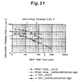
- Fig. 21 is a graph of the comparison between the discharge delay time in the case when a powder of MgO single crystals is dispersed in a medium such as a specific alcohol and then the suspension is sprayed to the surfaces of the dielectric layer 12 and the additional dielectric layers 12A by an air spray method using a spray gun to deposit the powder of MgO single crystals in order to form the MgO layer 13, and the discharge delay times in other examples.
- the graph a shows the discharge probabilities when a powder layer formed of a powder of vapor-phase MgO single crystals of an average particle diameter of 500 angstroms is formed on the surface of the dielectric layer 12.
- the graph b shows the discharge probabilities when a conventional vapor deposition technique is used to form an MgO layer on the surface of the dielectric layer.
- the graph c shows the discharge probabilities when, as described in the first embodiment example, in a PDP of the type having the discharge cells each divided into a display discharge cell and an address discharge cell, an MgO layer is formed in the address discharge cell by application of a coating of a paste including a powder of vapor-phase MgO single crystals of an average particle diameter of 500 angstroms.
- the graph d shows the discharge probabilities when in an address discharge cell of a similar type, an MgO layer is formed by a conventional vapor deposition technique.
- the discharge probabilities are greatly improved, either when, by use of the vapor-phase MgO single crystals of an average particle diameter of 500 angstroms, a coating is applied by a method such as screen printing, offset printing, dispenser technique, ink-jet technique or roll-coating technique to form an MgO layer, or when an MgO layer is formed by deposition using a method such as a spraying technique or electrostatic coating technique.
- Figs. 22 to 24 illustrate a third embodiment example of an embodiment of the PDP according to the invention.
- Fig. 22 is a schematic front view of the PDP in the third embodiment example.
- Fig. 23 is a sectional view taken along the V4-V4 line in Fig. 22
- Fig. 24 is a sectional view taken along the W3-W3 line in Fig. 22 .
- the PDP shown in Figs. 22 to 24 has a plurality of row electrode pairs (X2, Y2) arranged in parallel on a rear-facing face of a front glass substrate 21 serving as the display surface so as to extend in the row direction (the right-left direction in Fig. 22 ) of the front glass substrate 21.
- a row electrode X2 is composed of T-shaped transparent electrodes X2a formed of a transparent conductive film made of ITO or the like, and a bus electrode X2b which is formed of a metal film and which extends in the row direction of the front glass substrate 21 and is connected to the narrow proximal ends of the transparent electrodes X2a.
- a row electrode Y2 is composed of T-shaped transparent electrodes Y2a formed of a transparent conductive film made of ITO or the like, and a bus electrode Y2b which is formed of a metal film and which extends in the row direction of the front glass substrate 21 and is connected to the narrow proximal ends of the transparent electrodes Y2a.
- the row electrodes X2 and Y2 are arranged in alternate positions in the column direction of the front glass substrate 21 (the vertical direction in Fig. 22 ).
- the transparent electrodes X2a and Y2a which are regularly spaced along the associated bus electrodes X2b and Y2b, each extend out toward their counterparts in the row electrode pair, so that the wide distal ends of the transparent electrodes X2a and Y2a face each other across a discharge gap g 2 of a required width.
- Black or dark-colored light absorption layers (light-shield layers) 22 are each formed on the rear-facing face of the front glass substrate 21 between the back-to-back bus electrodes X2b and Y2b of the row electrode pairs (X2, Y2) adjacent to each other in the column direction, and extend along these bus electrodes X2b, Y2b in the row direction.
- a dielectric layer 23 is formed on the rear-facing face of the front glass substrate 21 so as to cover the row electrode pairs (X2, Y2).
- additional dielectric layers 23A which project backward from the dielectric layer 23, are each formed in a position opposite to the back-to-back bus electrodes X2b and Y2b of the row electrode pairs (X2, Y2) adjacent to each other and to the area between the above bus electrode X2b and the above bus electrode Y2b positioned back to back, so as to extend parallel to the bus electrodes X2b, Y2b.
- an MgO layer (hereinafter referred to as "thin-film MgO layer") 24 of a thin film formed by vapor deposition or spattering is formed and covers the rear-facing faces of the dielectric layer 23 and the additional dielectric layers 23A.
- crystalline MgO layers including MgO crystals causing a cathode-luminescence emission (CL emission) having a peak within a wavelength range of 200nm to 300nm (in particular, around 235nm, of 230nm to 250nm) upon excitation by electron beams as described in detail later is formed on the rear-facing face of the thin-film MgO layer 24.
- the crystalline MgO layer 25 is formed on either the entire rear-facing face or a part of the rear-facing face of the thin-film MgO layer 24, for example a part facing a discharge cell which will be described later (in the example illustrated in the figures, the crystalline MgO layer 25 is formed on the entire rear-facing face of the thin-film MgO layer 24).
- column electrodes D2 are arranged in parallel to each other at predetermined intervals so as to extend in a direction at right angles to the row electrode pairs (X2, Y2) (the column direction) through positions opposite to the paired transparent electrodes X2a and Y2a in each row electrode pair (X2, Y2).
- a white column-electrode protective layer (dielectric layer) 27 covering the column electrodes D2 is further formed on the display-side face of the back glass substrate 26, and in turn partition units 28 are formed on the column-electrode protective layer 27.
- Each of the partition units 28 is formed in a ladder shape made up of a pair of transverse walls 28A extending in the row direction in the respective positions opposite to the bus electrodes X2b and Y2b of each row electrode pair (X2, Y2), and vertical walls 28B each extending in the column direction between the pair of transverse walls 28A in a mid-position between the adjacent column electrodes D2.
- the partition units 28 are regularly arranged in the column direction on either side of an interstice SL which extends in the row direction between the back-to-back transverse walls 28A of the adjacent partition units 28.
- the ladder-shaped partition units 28 partition the discharge space S1 between the front glass substrate 21 and the back glass substrate 26 into quadrangles respectively corresponding to discharge cells C4 formed in relation to the paired transparent electrodes X2a and Y2a in each row electrode pair (X2, Y2).
- a phosphor layer 29 is formed on the side faces of the transverse walls 28A and the vertical walls 28B of the partition unit 28 and the face of the column-electrode protective layer 27 which face toward the discharge space S1, so as to cover all these five faces.
- the arrangement of the colors of the phosphor layers 29 is the three primary colors, red, green and blue, in sequence in the row direction in the respective discharge cells C4.
- the crystalline MgO layer 25 (or the thin-film MgO layer 24 if the crystalline MgO layer 25 is formed only a portion of the rear-facing face of the thin-film MgO layer 24 facing each discharge cell C4) covering the additional dielectric layers 23A is in contact with the display-side faces of the transparent walls 28A of the partition units 28 (see Fig. 23 ), whereby each additional dielectric layer 23A blocks off the discharge cell C4 and the interstice SL from each other.
- the crystalline MgO layer 25 (or the thin-film MgO layer 24) is out of contact with the display-side face of the vertical wall 28B (see Fig. 24 ), to form a clearance r 2 therebetween, so that the adjacent discharge cells C4 in the row direction communicate with each other by means of the clearance r 2.
- the discharge space S1 is filled with a discharge gas including xenon.
- the crystalline MgO layer 25 is formed by depositing MgO crystals, as described earlier, to the surface of the rear-facing face of the thin-film MgO layer 24 covering the dielectric layer 23 and the additional dielectric layers 23A by a method such as a spraying technique or electrostatic coating technique.
- the embodiment example describes the case where the thin-film MgO layer 24 is formed on the rear-facing faces of the dielectric layer 23 and the additional dielectric layers 23A and then the crystalline MgO layer 25 is formed on the rear-facing face of the thin-film MgO layer 24.
- the thin-film MgO layer 24 may be formed on the rear-facing face of the crystalline MgO layer 25 after the crystalline MgO layer 25 may be formed on the rear-facing faces of the dielectric layer 23 and the additional dielectric layers 23A.
- Fig. 25 illustrates the state when the thin-film MgO layer 24 is formed on the rear-facing face of the dielectric layer 23 and then MgO crystals are deposited to the rear-facing face of the thin-film MgO layer 24 to form the crystalline MgO layer 25 by use of a method such as a spraying technique or electrostatic coating technique.
- Fig. 26 illustrates the state when MgO crystals are deposited to the rear-facing face of the dielectric layer 23 to form the crystalline MgO layer 25 by use of a method such as a spraying technique or electrostatic coating technique, and then the thin-film MgO layer 24 is formed.
- the crystalline MgO layer 25 of the foregoing PDP is formed by use of the following materials and method.
- MgO crystals which are used as materials for forming the crystalline MgO layer 25 and causes CL emission having a peak within a wavelength range of 200nm to 300nm (in particular, around 235nm, of 230nm to 250nm) upon being excited by an electron beam
- a single crystal of magnesium obtained by performing vapor-phase oxidation on magnesium steam generated by heating magnesium (this single crystal of magnesium is hereinafter referred to as "vapor-phase MgO single crystal"
- vapor-phase MgO single crystal an MgO single crystal having a cubic single crystal structure as illustrated in the SEM photograph in Fig. 5
- an MgO single crystal having a structure of cubic crystals fitted to each other i.e. a cubic polycrystal structure
- the vapor-phase MgO single crystal contributes to an improvement of the discharge characteristics such as a reduction in discharge delay as described later.
- the vapor-phase MgO single crystal has the features of being of a high purity, taking a microscopic particle form, causing less particle agglomeration, and the like.
- the vapor-phase MgO single crystal used in the embodiment example has an average particle diameter of 500 or more angstroms (preferably, 2000 or more angstroms) based on a measurement using the BET method.
- the crystalline MgO layer 25 is formed, for example, by depositing the vapor-phase MgO single crystal by use of a method such as a spraying technique or electrostatic coating technique, as described earlier.
- a reset discharge, an address discharge and a sustaining discharge for generating an image are produced in the discharge cell C4.
- the priming effect resulting from the reset discharge lasts for a long time because of the formation of the crystalline MgO layer 25 in the discharge cell C4, thereby speeding up of the address discharge.
- the crystalline MgO layer 25 is formed of a vapor-phase MgO single crystal as described above, whereby the application of electron beams caused by the discharge excites, in addition to a CL emission having a peak within a wavelength range of 300nm to 400nm, a CL emission having a peak within a wavelength range of 200nm to 300nm (in particular, around 235nm, of 230nm to 250nm) from the large-particle-diameter vapor-phase MgO single crystals included in the crystalline MgO layer 25.
- the greater the particle diameter of the vapor-phase MgO single crystal the stronger the peak intensity of the CL emission having a peak within the wavelength range from 200nm to 300nm (in particular, around 235nm, of 230nm to 250nm).
- the CL emission with a peak at 235nm is not excited from a MgO layer formed typically by vapor deposition (corresponding to the thin-film MgO layer 24 in this embodiment example), but only a CL emission having a peak wavelengths from 300nm to 400nm is excited.
- the conjectured reason for the improvement of the discharge characteristics caused by the crystalline MgO layer 25 is because the vapor-phase MgO single crystals causing the CL emission having a peak within the wavelength range from 200nm to 300nm (in particular, around 235nm, of 230nm to 250nm) have an energy level corresponding to the peak wavelength, so that the energy level enables the trapping of electrons for a long time (some msec. or more), and the trapped electrons are extracted by an electric field so as to serve as the primary electrons required for starting a discharge.
- the reason that the stronger the intensity of the CL emission having a peak within the wavelength range from 200nm to 300nm (in particular, around 235nm, of 230nm to 250nm), the greater the improvement effects of the discharge characteristics caused by the vapor-phase MgO single crystal is as described in the aforementioned first embodiment example.
- the particle diameter (D BET ) of the vapor-phase MgO single crystals forming the crystalline MgO layer 25 is calculated by the same method as that in the first embodiment example.
- the correlation between the CL emission intensities and the discharge delay is, as is the case shown in Fig. 10 in the first embodiment example, that the display delay in the PDP is shortened by the 235nm CL emission excited from the crystalline MgO layer 25, and further, as the intensity of the 235nm CL emission increases, the discharge delay is shortened.
- Fig. 27 shows the comparison of the discharge delay characteristics between the case of the PDP having the double-layer structure of the thin-film MgO layer 24 and the crystalline MgO layer 25 as described above (Graph a ), and the case of a conventional PDP having only a MgO layer formed by vapor deposition (Graph b ).
- a PDP is provided with the double-layer structure of the thin-film MgO layer 24 and the crystalline MgO layer 25, whereby the discharge delay characteristics is significantly improved as compared with a conventional PDP having only a thin-film MgO layer formed by vapor deposition.
- the above-described PDP is improved in the discharge characteristics such as the discharge delay, and is capable of showing satisfactory discharge characteristics.
- the crystalline MgO layer 25 is not necessary required to be formed so as to cover the entire face of the thin-film MgO layer 24 as described earlier, and may be formed by patterning partially on portions facing the transparent electrodes X2a, Y2a of the row electrodes X2, Y2 or on portions excepting portions facing the transparent electrodes X2a, Y2a, for example.
- the area ratio of the crystalline MgO layers 25 to the thin-film MgO layer 24 is set at from 0.1 to 85 percent.
- the present invention is applicable to various types of PDPs, such as a reflection-type AC PDP having row electrode pairs and column electrodes formed on the front glass substrate and covered with a dielectric layer, and having phosphor layers formed on the back glass substrate; a transmission-type AC PDP having phosphor layers formed on the front glass substrate, and row electrode pairs and column electrodes formed on the back glass substrate and covered with a dielectric layer; a three-electrode AC PDP having discharge cells formed in positions corresponding to the intersections between row electrode pairs and column electrodes in the discharge space; a two-electrode AC PDP having discharge cells formed in positions corresponding to the intersections between row electrode pairs and column electrodes in the discharge space.
- the crystalline MgO layer 25 is formed through deposition by use of a method such as a spraying technique or an electrostatic coating technique.
- the crystalline MgO layer 25 may be formed through application of a coating of a paste including a powder of MgO crystals by use of a method such as a screen printing technique, an offset printing technique, a dispenser technique, an ink-jet technique of a roll-coating technique, or alternatively may be formed by applying a paste including MgO crystals to a support film, then drying it to a film and then laminating the film on the thin-film MgO layer.
- the invention is useful to provide a PDP improved in discharge characteristics such as discharge probabilities and discharge delay to provide satisfactory discharge characteristics.
Abstract
Claims (15)
- Ecran plasma équipé d'un substrat avant (1) et d'un substrat arrière (4) se faisant face l'un l'autre de part et d'autre d'un espace de décharge, et avec, entre le substrat avant (1) et le substrat arrière (4), une pluralité de paires d'électrodes en rangées (X, Y) et une pluralité d'électrodes en colonnes (D) s'étendant dans une direction croisant les paires d'électrodes en rangées (X, Y) pour former des zones luminescentes unitaires (C) dans les parties respectives de l'espace de décharge correspondant aux intersections avec les paires d'électrodes en rangées (X, Y), caractérisé par la disposition :sur une zone faisant face à la zone luminescente unitaire entre le substrat avant (1) et le substrat arrière (4), d'une couche d'oxyde de magnésium qui comprend un cristal d'oxyde de magnésium provoquant une émission de luminescence cathodique ayant un pic à une longueur d'onde située dans la plage allant de 200 nm à 300 nm après excitation par des faisceaux d'électrons.
- Ecran plasma selon la revendication 1, dans lequel le cristal d'oxyde de magnésium est un monocristal d'oxyde de magnésium.
- Ecran plasma selon la revendication 1, dans lequel le cristal d'oxyde de magnésium provoque une émission de luminescence cathodique ayant un pic à une longueur d'onde située dans la plage allant de 230 nm à 250 nm.
- Ecran plasma selon la revendication 1, dans lequel le cristal d'oxyde de magnésium a un diamètre de particule de 2000 angströms ou plus.
- Ecran plasma selon la revendication 1, dans lequel la couche d'oxyde de magnésium est formée sur une couche diélectrique (2) recouvrant les paires d'électrodes en rangées (X, Y).
- Ecran plasma selon la revendication 1, dans lequel la zone luminescente unitaire est divisée en une première zone luminescente (C1) pour provoquer une émission de lumière pour former une image et une deuxième zone luminescente (C2) pour initier une décharge pour sélectionner la première zone luminescente (C1) afin qu'elle provoque une émission de lumière pour former l'image, et la couche d'oxyde de magnésium (8) est disposée dans une zone faisant face à la deuxième zone luminescente (C2) de la zone luminescente unitaire.
- Ecran plasma selon la revendication 2, dans lequel le monocristal d'oxyde de magnésium a un diamètre de particule de 500 angströms ou plus.
- Ecran plasma selon la revendication 2, dans lequel le monocristal d'oxyde de magnésium a un diamètre de particule de 2000 angströms ou plus.
- Procédé pour fabriquer un écran plasma équipé d'un substrat avant (1) et d'un substrat arrière (4) se faisant face l'un l'autre de part et d'autre d'un espace de décharge, d'électrodes (X, Y, D) formées sur au moins l'un des substrats avant et arrière, d'une couche diélectrique (2, 5) recouvrant les électrodes (X, Y, D) et d'une couche protectrice recouvrant la couche diélectrique (2), caractérisé en ce qu'il comprend :un procédé de formation d'une couche d'oxyde de magnésium (8) qui comprend un cristal d'oxyde de magnésium provoquant une émission de luminescence cathodique ayant un pic à une longueur d'onde située dans la plage allant de 200 nm à 300 nm après excitation par des faisceaux d'électrons, en une position recouvrant une partie requise de la couche diélectrique.
- Procédé pour fabriquer un écran plasma selon la revendication 9, dans lequel, dans le procédé de formation de l'oxyde de magnésium (8), une poudre du cristal d'oxyde de magnésium est pulvérisée et déposée sur la couche diélectrique (5) pour former la couche d'oxyde de magnésium (8).
- Procédé pour fabriquer un écran plasma selon la revendication 9, dans lequel le cristal d'oxyde de magnésium est un monocristal d'oxyde de magnésium produit par une technique d'oxydation en phase vapeur.
- Procédé pour fabriquer un écran plasma selon la revendication 9, dans lequel le cristal d'oxyde de magnésium provoque une émission de luminescence cathodique ayant un pic à une longueur d'onde située dans la plage allant de 230 nm à 250 nm.
- Procédé pour fabriquer un écran plasma selon la revendication 9, dans lequel le cristal d'oxyde de magnésium a un diamètre de particule de 2000 angströms ou plus.
- Procédé pour fabriquer un écran plasma selon la revendication 11, dans lequel le monocristal d'oxyde de magnésium a un diamètre de particule de 500 angströms ou plus.
- Procédé pour fabriquer un écran plasma selon la revendication 11, dans lequel le monocristal d'oxyde de magnésium a un diamètre de particule de 2000 angströms ou plus.
Priority Applications (3)
| Application Number | Priority Date | Filing Date | Title |
|---|---|---|---|
| EP11004074.8A EP2360710B1 (fr) | 2003-09-26 | 2004-09-17 | Ecran plasma et son procédé de fabrication |
| EP11004073.0A EP2360709B1 (fr) | 2003-09-26 | 2004-09-17 | Ecran d'affichage plasma et son procédé de production |
| EP11004075A EP2369611A1 (fr) | 2003-09-26 | 2004-09-17 | Ecran plasma et son procede de fabrication |
Applications Claiming Priority (8)
| Application Number | Priority Date | Filing Date | Title |
|---|---|---|---|
| JP2003335866 | 2003-09-26 | ||
| JP2004052194 | 2004-02-26 | ||
| JP2004052193 | 2004-02-26 | ||
| JP2004212959 | 2004-07-21 | ||
| JP2004212960 | 2004-07-21 | ||
| JP2004262988A JP3878635B2 (ja) | 2003-09-26 | 2004-09-09 | プラズマディスプレイパネルおよびその製造方法 |
| JP2004262989A JP3842276B2 (ja) | 2004-02-26 | 2004-09-09 | プラズマディスプレイパネルおよびその製造方法 |
| PCT/JP2004/013641 WO2005031782A1 (fr) | 2003-09-26 | 2004-09-17 | Ecran d'affichage plasma et son procede de production |
Related Child Applications (3)
| Application Number | Title | Priority Date | Filing Date |
|---|---|---|---|
| EP11004074.8 Division-Into | 2011-05-17 | ||
| EP11004075.5 Division-Into | 2011-05-17 | ||
| EP11004073.0 Division-Into | 2011-05-17 |
Publications (3)
| Publication Number | Publication Date |
|---|---|
| EP1667190A1 EP1667190A1 (fr) | 2006-06-07 |
| EP1667190A4 EP1667190A4 (fr) | 2009-04-01 |
| EP1667190B1 true EP1667190B1 (fr) | 2011-11-16 |
Family
ID=34397290
Family Applications (4)
| Application Number | Title | Priority Date | Filing Date |
|---|---|---|---|
| EP04773276A Expired - Fee Related EP1667190B1 (fr) | 2003-09-26 | 2004-09-17 | Ecran plasma et son procede de fabrication |
| EP11004075A Withdrawn EP2369611A1 (fr) | 2003-09-26 | 2004-09-17 | Ecran plasma et son procede de fabrication |
| EP11004073.0A Expired - Fee Related EP2360709B1 (fr) | 2003-09-26 | 2004-09-17 | Ecran d'affichage plasma et son procédé de production |
| EP11004074.8A Expired - Fee Related EP2360710B1 (fr) | 2003-09-26 | 2004-09-17 | Ecran plasma et son procédé de fabrication |
Family Applications After (3)
| Application Number | Title | Priority Date | Filing Date |
|---|---|---|---|
| EP11004075A Withdrawn EP2369611A1 (fr) | 2003-09-26 | 2004-09-17 | Ecran plasma et son procede de fabrication |
| EP11004073.0A Expired - Fee Related EP2360709B1 (fr) | 2003-09-26 | 2004-09-17 | Ecran d'affichage plasma et son procédé de production |
| EP11004074.8A Expired - Fee Related EP2360710B1 (fr) | 2003-09-26 | 2004-09-17 | Ecran plasma et son procédé de fabrication |
Country Status (6)
| Country | Link |
|---|---|
| US (1) | US7626336B2 (fr) |
| EP (4) | EP1667190B1 (fr) |
| KR (2) | KR101099251B1 (fr) |
| CN (1) | CN100559540C (fr) |
| TW (1) | TW200514114A (fr) |
| WO (1) | WO2005031782A1 (fr) |
Families Citing this family (39)
| Publication number | Priority date | Publication date | Assignee | Title |
|---|---|---|---|---|
| KR100612297B1 (ko) * | 2003-10-24 | 2006-08-11 | 삼성에스디아이 주식회사 | 보호막을 개선한 플라즈마 디스플레이 패널 |
| JP4541832B2 (ja) * | 2004-03-19 | 2010-09-08 | パナソニック株式会社 | プラズマディスプレイパネル |
| JP4683547B2 (ja) * | 2004-09-16 | 2011-05-18 | パナソニック株式会社 | プラズマディスプレイパネル |
| JP4541840B2 (ja) * | 2004-11-08 | 2010-09-08 | パナソニック株式会社 | プラズマディスプレイパネル |
| JP4399344B2 (ja) | 2004-11-22 | 2010-01-13 | パナソニック株式会社 | プラズマディスプレイパネルおよびその製造方法 |
| JP4704109B2 (ja) * | 2005-05-30 | 2011-06-15 | パナソニック株式会社 | プラズマディスプレイ装置 |
| JP4987256B2 (ja) * | 2005-06-22 | 2012-07-25 | パナソニック株式会社 | プラズマディスプレイ装置 |
| JP4987255B2 (ja) * | 2005-06-22 | 2012-07-25 | パナソニック株式会社 | プラズマディスプレイ装置 |
| JP4987258B2 (ja) * | 2005-07-07 | 2012-07-25 | パナソニック株式会社 | プラズマディスプレイ装置 |
| JP2007072266A (ja) * | 2005-09-08 | 2007-03-22 | Pioneer Electronic Corp | プラズマディスプレイ装置 |
| JP4972302B2 (ja) * | 2005-09-08 | 2012-07-11 | パナソニック株式会社 | プラズマディスプレイ装置 |
| JP4976684B2 (ja) * | 2005-11-04 | 2012-07-18 | パナソニック株式会社 | プラズマディスプレイ装置 |
| EP1833070A3 (fr) * | 2006-03-10 | 2008-12-03 | Pioneer Corporation | Panneau d'affichage à plasma de type de décharge de surface |
| KR100768223B1 (ko) * | 2006-04-12 | 2007-10-17 | 삼성에스디아이 주식회사 | 디스플레이 장치 |
| JP4148986B2 (ja) * | 2006-05-31 | 2008-09-10 | 松下電器産業株式会社 | プラズマディスプレイパネル |
| US8222814B2 (en) * | 2006-10-20 | 2012-07-17 | Panasonic Corporation | Plasma display panel with exposed crystal particles and manufacturing method thereof |
| US8026668B2 (en) * | 2007-01-23 | 2011-09-27 | Panasonic Corporation | Plasma display panel and method for driving same |
| JP5016935B2 (ja) * | 2007-01-30 | 2012-09-05 | タテホ化学工業株式会社 | 立方体状酸化マグネシウム粉末及びその製法 |
| JP5134264B2 (ja) * | 2007-03-02 | 2013-01-30 | パナソニック株式会社 | プラズマディスプレイパネルの駆動方法 |
| EP1968036A3 (fr) * | 2007-03-06 | 2010-07-14 | Panasonic Corporation | Procédé de commande d'un panneau d'affichage à plasma |
| JP5236893B2 (ja) * | 2007-04-25 | 2013-07-17 | タテホ化学工業株式会社 | 酸化物発光体 |
| JP2008311203A (ja) * | 2007-06-15 | 2008-12-25 | Seoul National Univ Industry Foundation | 特定の負極発光特性を有する酸化マグネシウムの微粒子を含むプラズマ素子 |
| KR20090021733A (ko) * | 2007-08-28 | 2009-03-04 | 엘지전자 주식회사 | 플라즈마 디스플레이 패널 및 그 제조방법 |
| US8207672B2 (en) * | 2007-10-02 | 2012-06-26 | Hitachi, Ltd | Plasma display panel having a discharge stabilizer powder and method of manufacturing the same |
| KR100927623B1 (ko) * | 2007-11-20 | 2009-11-20 | 삼성에스디아이 주식회사 | 플라즈마 디스플레이 패널 |
| KR100943194B1 (ko) * | 2007-12-14 | 2010-02-19 | 삼성에스디아이 주식회사 | 마그네슘 산화물 입자가 표면에 부착된 플라즈마디스플레이 패널용 보호막, 이의 제조 방법 및 상기보호막을 구비한 플라즈마 디스플레이 패널 |
| JP2009253790A (ja) * | 2008-04-09 | 2009-10-29 | Panasonic Corp | 操作記録同時再生システム |
| KR20090118266A (ko) * | 2008-05-13 | 2009-11-18 | 삼성에스디아이 주식회사 | 플라즈마 디스플레이 패널 |
| JP2010009900A (ja) * | 2008-06-26 | 2010-01-14 | Panasonic Corp | プラズマディスプレイパネルの製造方法 |
| JP5012698B2 (ja) * | 2008-06-30 | 2012-08-29 | パナソニック株式会社 | プラズマディスプレイパネル用金属酸化物ペースト及びプラズマディスプレイパネルの製造方法 |
| JP2010015699A (ja) * | 2008-07-01 | 2010-01-21 | Panasonic Corp | プラズマディスプレイパネルの製造方法及びプラズマディスプレイパネル用金属酸化物ペーストの製造方法 |
| JP5251355B2 (ja) * | 2008-08-20 | 2013-07-31 | パナソニック株式会社 | プラズマディスプレイパネルの製造方法 |
| JP5090401B2 (ja) * | 2009-05-13 | 2012-12-05 | パナソニック株式会社 | プラズマディスプレイパネルの製造方法 |
| US9336028B2 (en) | 2009-06-25 | 2016-05-10 | Apple Inc. | Virtual graphics device driver |
| JP5161173B2 (ja) * | 2009-08-26 | 2013-03-13 | パナソニック株式会社 | プラズマディスプレイパネルの製造方法 |
| JP4972173B2 (ja) * | 2010-01-13 | 2012-07-11 | パナソニック株式会社 | プラズマディスプレイパネルの製造方法 |
| US8513888B2 (en) | 2010-03-15 | 2013-08-20 | Panasonic Corporation | Plasma display panel |
| US8482190B2 (en) | 2010-03-15 | 2013-07-09 | Panasonic Corporation | Plasma display panel |
| WO2011114697A1 (fr) | 2010-03-15 | 2011-09-22 | パナソニック株式会社 | Panneau d'affichage à plasma |
Citations (4)
| Publication number | Priority date | Publication date | Assignee | Title |
|---|---|---|---|---|
| JPH07147149A (ja) * | 1993-11-24 | 1995-06-06 | Matsushita Electric Ind Co Ltd | 平板型画像表示装置およびその製造法 |
| JPH09167566A (ja) * | 1995-12-15 | 1997-06-24 | Fujitsu Ltd | プラズマディスプレイパネル及びその製造方法 |
| JPH11213869A (ja) * | 1998-01-21 | 1999-08-06 | Asahi Glass Co Ltd | 交流型プラズマディスプレイパネルの保護膜の形成方法ならびにその装置 |
| JP2001118511A (ja) * | 1999-09-15 | 2001-04-27 | Koninkl Philips Electronics Nv | プラズマ画像スクリーン |
Family Cites Families (22)
| Publication number | Priority date | Publication date | Assignee | Title |
|---|---|---|---|---|
| US4604118A (en) * | 1985-08-13 | 1986-08-05 | Corning Glass Works | Method for synthesizing MgO--Al2 O3 --SiO2 glasses and ceramics |
| JP2731854B2 (ja) * | 1989-02-10 | 1998-03-25 | 協和化学工業株式会社 | 高耐水和性、高流動性酸化マグネシウムの製造方法 |
| JP3459933B2 (ja) * | 1993-05-10 | 2003-10-27 | 平樹 内池 | ac形プラズマディスプレイおよびその製造方法 |
| JP3476217B2 (ja) | 1993-07-26 | 2003-12-10 | 富士通株式会社 | プラズマディスプレイパネル |
| JPH07192630A (ja) * | 1993-12-27 | 1995-07-28 | Oki Electric Ind Co Ltd | ガス放電表示パネル及びその保護膜形成方法 |
| JP2571015B2 (ja) | 1994-04-27 | 1997-01-16 | 日本電気株式会社 | ガス放電表示パネルの製造方法 |
| JPH08287823A (ja) * | 1995-04-17 | 1996-11-01 | Oki Electric Ind Co Ltd | 交流型ガス放電パネルの保護膜形成方法 |
| JP3339554B2 (ja) * | 1995-12-15 | 2002-10-28 | 松下電器産業株式会社 | プラズマディスプレイパネル及びその製造方法 |
| KR19980065367A (ko) * | 1996-06-02 | 1998-10-15 | 오평희 | 액정표시소자용 백라이트 |
| US6013309A (en) * | 1997-02-13 | 2000-01-11 | Lg Electronics Inc. | Protection layer of plasma display panel and method of forming the same |
| JP2000156153A (ja) | 1998-11-17 | 2000-06-06 | Dainippon Printing Co Ltd | 二次電子放出膜の製造方法及び二次電子放出膜 |
| KR100899311B1 (ko) * | 1998-12-10 | 2009-05-27 | 미쓰비시 마테리알 가부시키가이샤 | Fpd 용 보호막 및 그 제조방법 그리고 이것을 사용한 fpd |
| JP3623406B2 (ja) | 1999-09-07 | 2005-02-23 | 松下電器産業株式会社 | ガス放電パネルとその製造方法 |
| US6492770B2 (en) * | 2000-02-07 | 2002-12-10 | Pioneer Corporation | Plasma display panel |
| JP4248721B2 (ja) * | 2000-02-22 | 2009-04-02 | 三菱電機株式会社 | 紫外線変換材料とこの紫外線変換材料を用いた表示装置 |
| EP1298694B1 (fr) | 2000-05-11 | 2010-06-23 | Panasonic Corporation | Film mince a emission d'electrons, ecran a plasma comportant un tel film et procede de fabrication dudit film et dudit ecran |
| JP4153983B2 (ja) | 2000-07-17 | 2008-09-24 | パイオニア株式会社 | 保護膜、その成膜方法、プラズマディスプレイパネル及びその製造方法 |
| JP4878425B2 (ja) * | 2000-08-29 | 2012-02-15 | パナソニック株式会社 | プラズマディスプレイパネルおよびその製造方法ならびにプラズマディスプレイパネル表示装置 |
| WO2002019368A1 (fr) * | 2000-08-29 | 2002-03-07 | Matsushita Electric Industrial Co., Ltd. | Ecran a plasma et son procede de production et unite d'affichage d'ecran a plasma |
| US6674238B2 (en) * | 2001-07-13 | 2004-01-06 | Pioneer Corporation | Plasma display panel |
| JP2003031130A (ja) | 2001-07-13 | 2003-01-31 | Pioneer Electronic Corp | プラズマディスプレイパネル |
| JP2003151445A (ja) * | 2001-11-09 | 2003-05-23 | Pioneer Electronic Corp | プラズマディスプレイパネルおよびその駆動方法 |
-
2004
- 2004-09-17 KR KR1020067004477A patent/KR101099251B1/ko not_active IP Right Cessation
- 2004-09-17 CN CNB2004800234174A patent/CN100559540C/zh not_active Expired - Fee Related
- 2004-09-17 EP EP04773276A patent/EP1667190B1/fr not_active Expired - Fee Related
- 2004-09-17 EP EP11004075A patent/EP2369611A1/fr not_active Withdrawn
- 2004-09-17 EP EP11004073.0A patent/EP2360709B1/fr not_active Expired - Fee Related
- 2004-09-17 US US10/573,446 patent/US7626336B2/en not_active Expired - Fee Related
- 2004-09-17 WO PCT/JP2004/013641 patent/WO2005031782A1/fr active Application Filing
- 2004-09-17 KR KR1020117005960A patent/KR101031581B1/ko not_active IP Right Cessation
- 2004-09-17 EP EP11004074.8A patent/EP2360710B1/fr not_active Expired - Fee Related
- 2004-09-23 TW TW093128863A patent/TW200514114A/zh unknown
Patent Citations (4)
| Publication number | Priority date | Publication date | Assignee | Title |
|---|---|---|---|---|
| JPH07147149A (ja) * | 1993-11-24 | 1995-06-06 | Matsushita Electric Ind Co Ltd | 平板型画像表示装置およびその製造法 |
| JPH09167566A (ja) * | 1995-12-15 | 1997-06-24 | Fujitsu Ltd | プラズマディスプレイパネル及びその製造方法 |
| JPH11213869A (ja) * | 1998-01-21 | 1999-08-06 | Asahi Glass Co Ltd | 交流型プラズマディスプレイパネルの保護膜の形成方法ならびにその装置 |
| JP2001118511A (ja) * | 1999-09-15 | 2001-04-27 | Koninkl Philips Electronics Nv | プラズマ画像スクリーン |
Non-Patent Citations (1)
| Title |
|---|
| GANDY H: "Cathodoluminescence of strontium oxide, barium-strontium oxide and magnesium oxide", INSPEC,, 1 August 1958 (1958-08-01), XP002503919 * |
Also Published As
| Publication number | Publication date |
|---|---|
| EP1667190A1 (fr) | 2006-06-07 |
| CN100559540C (zh) | 2009-11-11 |
| CN1836305A (zh) | 2006-09-20 |
| KR20110031508A (ko) | 2011-03-28 |
| EP1667190A4 (fr) | 2009-04-01 |
| EP2360710B1 (fr) | 2013-05-22 |
| KR101099251B1 (ko) | 2011-12-28 |
| WO2005031782A1 (fr) | 2005-04-07 |
| US20070013306A1 (en) | 2007-01-18 |
| TW200514114A (en) | 2005-04-16 |
| US7626336B2 (en) | 2009-12-01 |
| EP2360709B1 (fr) | 2013-11-20 |
| EP2360709A1 (fr) | 2011-08-24 |
| EP2369611A1 (fr) | 2011-09-28 |
| EP2360710A1 (fr) | 2011-08-24 |
| KR20070006661A (ko) | 2007-01-11 |
| KR101031581B1 (ko) | 2011-04-27 |
Similar Documents
| Publication | Publication Date | Title |
|---|---|---|
| EP1667190B1 (fr) | Ecran plasma et son procede de fabrication | |
| US8508129B2 (en) | Plasma display panel including metal oxide crystal powder and method of manufacturing same | |
| US7474055B2 (en) | Plasma display panel | |
| US7880387B2 (en) | Plasma display panel having a crystalline magnesium oxide layer | |
| US7567036B2 (en) | Plasma display panel with single crystal magnesium oxide layer | |
| US7535178B2 (en) | Plasma display panel | |
| US20060214585A1 (en) | Plasma display panel and method of manufacturing same | |
| JP2006059779A (ja) | プラズマディスプレイパネルおよびその製造方法 | |
| JP3842276B2 (ja) | プラズマディスプレイパネルおよびその製造方法 | |
| JP4657988B2 (ja) | プラズマディスプレイパネルおよびその製造方法 |
Legal Events
| Date | Code | Title | Description |
|---|---|---|---|
| PUAI | Public reference made under article 153(3) epc to a published international application that has entered the european phase |
Free format text: ORIGINAL CODE: 0009012 |
|
| AK | Designated contracting states |
Kind code of ref document: A1 Designated state(s): DE FR GB |
|
| 17P | Request for examination filed |
Effective date: 20060324 |
|
| DAX | Request for extension of the european patent (deleted) | ||
| RBV | Designated contracting states (corrected) |
Designated state(s): DE FR GB |
|
| A4 | Supplementary search report drawn up and despatched |
Effective date: 20090227 |
|
| 17Q | First examination report despatched |
Effective date: 20090507 |
|
| RAP1 | Party data changed (applicant data changed or rights of an application transferred) |
Owner name: PANASONIC CORPORATION |
|
| REG | Reference to a national code |
Ref country code: DE Ref legal event code: R079 Ref document number: 602004035343 Country of ref document: DE Free format text: PREVIOUS MAIN CLASS: H01J0011020000 Ipc: H01J0017160000 |
|
| GRAP | Despatch of communication of intention to grant a patent |
Free format text: ORIGINAL CODE: EPIDOSNIGR1 |
|
| RIC1 | Information provided on ipc code assigned before grant |
Ipc: H01J 9/02 20060101ALI20110420BHEP Ipc: H01J 9/24 20060101ALI20110420BHEP Ipc: H01J 17/49 20060101ALI20110420BHEP Ipc: H01J 17/16 20060101AFI20110420BHEP |
|
| GRAS | Grant fee paid |
Free format text: ORIGINAL CODE: EPIDOSNIGR3 |
|
| GRAA | (expected) grant |
Free format text: ORIGINAL CODE: 0009210 |
|
| AK | Designated contracting states |
Kind code of ref document: B1 Designated state(s): DE FR GB |
|
| REG | Reference to a national code |
Ref country code: GB Ref legal event code: FG4D |
|
| REG | Reference to a national code |
Ref country code: DE Ref legal event code: R096 Ref document number: 602004035343 Country of ref document: DE Effective date: 20120126 |
|
| PLBE | No opposition filed within time limit |
Free format text: ORIGINAL CODE: 0009261 |
|
| STAA | Information on the status of an ep patent application or granted ep patent |
Free format text: STATUS: NO OPPOSITION FILED WITHIN TIME LIMIT |
|
| 26N | No opposition filed |
Effective date: 20120817 |
|
| REG | Reference to a national code |
Ref country code: DE Ref legal event code: R097 Ref document number: 602004035343 Country of ref document: DE Effective date: 20120817 |
|
| REG | Reference to a national code |
Ref country code: DE Ref legal event code: R084 Ref document number: 602004035343 Country of ref document: DE |
|
| REG | Reference to a national code |
Ref country code: GB Ref legal event code: 746 Effective date: 20130617 |
|
| REG | Reference to a national code |
Ref country code: DE Ref legal event code: R084 Ref document number: 602004035343 Country of ref document: DE Effective date: 20130701 |
|
| REG | Reference to a national code |
Ref country code: FR Ref legal event code: PLFP Year of fee payment: 12 |
|
| PGFP | Annual fee paid to national office [announced via postgrant information from national office to epo] |
Ref country code: GB Payment date: 20150917 Year of fee payment: 12 Ref country code: DE Payment date: 20150922 Year of fee payment: 12 |
|
| PGFP | Annual fee paid to national office [announced via postgrant information from national office to epo] |
Ref country code: FR Payment date: 20150922 Year of fee payment: 12 |
|
| REG | Reference to a national code |
Ref country code: DE Ref legal event code: R119 Ref document number: 602004035343 Country of ref document: DE |
|
| GBPC | Gb: european patent ceased through non-payment of renewal fee |
Effective date: 20160917 |
|
| REG | Reference to a national code |
Ref country code: FR Ref legal event code: ST Effective date: 20170531 |
|
| PG25 | Lapsed in a contracting state [announced via postgrant information from national office to epo] |
Ref country code: GB Free format text: LAPSE BECAUSE OF NON-PAYMENT OF DUE FEES Effective date: 20160917 Ref country code: DE Free format text: LAPSE BECAUSE OF NON-PAYMENT OF DUE FEES Effective date: 20170401 Ref country code: FR Free format text: LAPSE BECAUSE OF NON-PAYMENT OF DUE FEES Effective date: 20160930 |