EP1661173B1 - Verfahren zur herstellung eines halbleiterbauelements mit ultraschmalem kanal - Google Patents
Verfahren zur herstellung eines halbleiterbauelements mit ultraschmalem kanal Download PDFInfo
- Publication number
- EP1661173B1 EP1661173B1 EP04778888A EP04778888A EP1661173B1 EP 1661173 B1 EP1661173 B1 EP 1661173B1 EP 04778888 A EP04778888 A EP 04778888A EP 04778888 A EP04778888 A EP 04778888A EP 1661173 B1 EP1661173 B1 EP 1661173B1
- Authority
- EP
- European Patent Office
- Prior art keywords
- region
- nanowire
- dielectric layer
- sacrificial
- source
- Prior art date
- Legal status (The legal status is an assumption and is not a legal conclusion. Google has not performed a legal analysis and makes no representation as to the accuracy of the status listed.)
- Expired - Lifetime
Links
Images


Classifications
-
- H—ELECTRICITY
- H10—SEMICONDUCTOR DEVICES; ELECTRIC SOLID-STATE DEVICES NOT OTHERWISE PROVIDED FOR
- H10D—INORGANIC ELECTRIC SEMICONDUCTOR DEVICES
- H10D30/00—Field-effect transistors [FET]
- H10D30/40—FETs having zero-dimensional [0D], one-dimensional [1D] or two-dimensional [2D] charge carrier gas channels
- H10D30/43—FETs having zero-dimensional [0D], one-dimensional [1D] or two-dimensional [2D] charge carrier gas channels having one-dimensional [1D] charge carrier gas channels, e.g. quantum wire FETs or transistors having 1D quantum-confined channels
-
- H—ELECTRICITY
- H10—SEMICONDUCTOR DEVICES; ELECTRIC SOLID-STATE DEVICES NOT OTHERWISE PROVIDED FOR
- H10P—GENERIC PROCESSES OR APPARATUS FOR THE MANUFACTURE OR TREATMENT OF DEVICES COVERED BY CLASS H10
- H10P14/00—Formation of materials, e.g. in the shape of layers or pillars
- H10P14/20—Formation of materials, e.g. in the shape of layers or pillars of semiconductor materials
-
- B—PERFORMING OPERATIONS; TRANSPORTING
- B82—NANOTECHNOLOGY
- B82Y—SPECIFIC USES OR APPLICATIONS OF NANOSTRUCTURES; MEASUREMENT OR ANALYSIS OF NANOSTRUCTURES; MANUFACTURE OR TREATMENT OF NANOSTRUCTURES
- B82Y10/00—Nanotechnology for information processing, storage or transmission, e.g. quantum computing or single electron logic
-
- H—ELECTRICITY
- H10—SEMICONDUCTOR DEVICES; ELECTRIC SOLID-STATE DEVICES NOT OTHERWISE PROVIDED FOR
- H10D—INORGANIC ELECTRIC SEMICONDUCTOR DEVICES
- H10D30/00—Field-effect transistors [FET]
- H10D30/01—Manufacture or treatment
- H10D30/014—Manufacture or treatment of FETs having zero-dimensional [0D] or one-dimensional [1D] channels, e.g. quantum wire FETs, single-electron transistors [SET] or Coulomb blockade transistors
-
- H—ELECTRICITY
- H10—SEMICONDUCTOR DEVICES; ELECTRIC SOLID-STATE DEVICES NOT OTHERWISE PROVIDED FOR
- H10D—INORGANIC ELECTRIC SEMICONDUCTOR DEVICES
- H10D30/00—Field-effect transistors [FET]
- H10D30/40—FETs having zero-dimensional [0D], one-dimensional [1D] or two-dimensional [2D] charge carrier gas channels
- H10D30/402—Single electron transistors; Coulomb blockade transistors
-
- H—ELECTRICITY
- H10—SEMICONDUCTOR DEVICES; ELECTRIC SOLID-STATE DEVICES NOT OTHERWISE PROVIDED FOR
- H10D—INORGANIC ELECTRIC SEMICONDUCTOR DEVICES
- H10D62/00—Semiconductor bodies, or regions thereof, of devices having potential barriers
- H10D62/10—Shapes, relative sizes or dispositions of the regions of the semiconductor bodies; Shapes of the semiconductor bodies
- H10D62/117—Shapes of semiconductor bodies
- H10D62/118—Nanostructure semiconductor bodies
- H10D62/119—Nanowire, nanosheet or nanotube semiconductor bodies
- H10D62/121—Nanowire, nanosheet or nanotube semiconductor bodies oriented parallel to substrates
-
- B—PERFORMING OPERATIONS; TRANSPORTING
- B82—NANOTECHNOLOGY
- B82Y—SPECIFIC USES OR APPLICATIONS OF NANOSTRUCTURES; MEASUREMENT OR ANALYSIS OF NANOSTRUCTURES; MANUFACTURE OR TREATMENT OF NANOSTRUCTURES
- B82Y40/00—Manufacture or treatment of nanostructures
-
- H—ELECTRICITY
- H10—SEMICONDUCTOR DEVICES; ELECTRIC SOLID-STATE DEVICES NOT OTHERWISE PROVIDED FOR
- H10D—INORGANIC ELECTRIC SEMICONDUCTOR DEVICES
- H10D30/00—Field-effect transistors [FET]
- H10D30/01—Manufacture or treatment
- H10D30/021—Manufacture or treatment of FETs having insulated gates [IGFET]
- H10D30/024—Manufacture or treatment of FETs having insulated gates [IGFET] of fin field-effect transistors [FinFET]
- H10D30/0245—Manufacture or treatment of FETs having insulated gates [IGFET] of fin field-effect transistors [FinFET] by further thinning the channel after patterning the channel, e.g. using sacrificial oxidation on fins
-
- H—ELECTRICITY
- H10—SEMICONDUCTOR DEVICES; ELECTRIC SOLID-STATE DEVICES NOT OTHERWISE PROVIDED FOR
- H10D—INORGANIC ELECTRIC SEMICONDUCTOR DEVICES
- H10D30/00—Field-effect transistors [FET]
- H10D30/60—Insulated-gate field-effect transistors [IGFET]
- H10D30/62—Fin field-effect transistors [FinFET]
-
- H—ELECTRICITY
- H10—SEMICONDUCTOR DEVICES; ELECTRIC SOLID-STATE DEVICES NOT OTHERWISE PROVIDED FOR
- H10D—INORGANIC ELECTRIC SEMICONDUCTOR DEVICES
- H10D64/00—Electrodes of devices having potential barriers
- H10D64/01—Manufacture or treatment
- H10D64/017—Manufacture or treatment using dummy gates in processes wherein at least parts of the final gates are self-aligned to the dummy gates, i.e. replacement gate processes
-
- Y—GENERAL TAGGING OF NEW TECHNOLOGICAL DEVELOPMENTS; GENERAL TAGGING OF CROSS-SECTIONAL TECHNOLOGIES SPANNING OVER SEVERAL SECTIONS OF THE IPC; TECHNICAL SUBJECTS COVERED BY FORMER USPC CROSS-REFERENCE ART COLLECTIONS [XRACs] AND DIGESTS
- Y10—TECHNICAL SUBJECTS COVERED BY FORMER USPC
- Y10S—TECHNICAL SUBJECTS COVERED BY FORMER USPC CROSS-REFERENCE ART COLLECTIONS [XRACs] AND DIGESTS
- Y10S977/00—Nanotechnology
- Y10S977/70—Nanostructure
- Y10S977/762—Nanowire or quantum wire, i.e. axially elongated structure having two dimensions of 100 nm or less
Definitions
- a method of fabricating an ultra-small nanowire and a semiconductor device having an ultra-narrow channel formed in the nanowire is a method of fabricating an ultra-small nanowire and a semiconductor device having an ultra-narrow channel formed in the nanowire.
- Nanoscale structures are being made on nanoscale structures since smaller devices typically equate to faster switching times, which lead to speedier and better performance.
- Devices based upon nanoscale structures having ultra-small dimensions are thus a natural progression of semiconductor device scaling.
- devices have been made on a semiconductor nanoscale structures generally known as "nanowire.”
- a nanowire is referred to as a semiconductor (e.g., silicon) structure having dimensions in the order of nanometers.
- Current methods of fabricating nanowires include photolithography and vapor liquid solid epitaxy deposition.
- a thin layer of semiconductor material e.g., silicon
- a substrate e.g., silicon
- metal colloids e.g., gold or nickel
- silicon source gas e.g., silane
- Silicon is then decomposed and grown on the colloids forming silicon nanowires.
- the silicon nanowires are removed from the colloids and are deposited on a substrate. Under both methods, the dimensions of the nanowires are difficult to control especially for dimensions less than 5 nm.
- Document US 5612255 discloses a silicon quantum wire transistor where a silicon substrate is sub-etched leaving a thin ridge ( ⁇ 500 ⁇ tall by ⁇ 500 ⁇ wide) of a silicon quantum wire, on the substrate surface from which a FET may be formed by depositing or growing gate oxide and depositing gate poly.
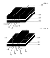
- Figure 1 illustrates a nanowire formed on a substrate
- Figure 2 illustrates a sacrificial gate stack formed over the nanowire of Figure 1 ;
- Figure 3 illustrates a sacrificial gate stack and two spacers formed adjacent to the sacrificial gate stack that is formed over the nanowire;
- Figure 4 illustrates a sacrificial gate stack, at least one spacer adjacent each side of the sacrificial gate stack, and a dielectric layer formed over the nanowire;
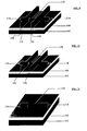
- Figure 5 illustrates the sacrificial gate stack of Figure 4 is removed to expose a section of the nanowire
- Figure 6 illustrates thinning of the exposed section of the nanowire of Figure 5 down to a desired dimension
- Figure 7 illustrates that a device gate stack formed over the thinned nanowire of Figure 6 to form a semiconductor device having an ultra-narrow channel region;
- Figure 8 illustrates the semiconductor device of Figure 7 with the dielectric layer removed for clarity purpose
- Figure 9 illustrates the semiconductor device of Figure 7 with the dielectric layer and the device gate stack removed for clarity purpose
- Figure 10 illustrates the semiconductor device of Figure 7 with the dielectric layer and the device gate stack removed, and only one spacer is shown for clarity purpose;
- Figure 11 illustrates the semiconductor device of Figure 7 with everything removed except for the nanowire having sections of different cross-sectional dimensions
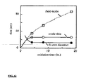
- Figure 12 shows that thermal oxidation of nanoscale semiconductor structure is self-limiting.
- nanoscale structures such as nanowires are extremely difficult to make with reliable and controllable dimensions.
- Current methods used to make nanowires include dimensional control of initial growth from nanometer sized nucleation sites or lithographic and patterning methods to print small dimensional structures that then use over-etching techniques to reduce the dimensions of the nanowires. These approaches can be difficult in practice, especially when trying to control the dimensions of billions of small regions across a giant 300mm wafer.
- Exemplary embodiments of the present invention describe methods of making nanowires that allow for easy control of the dimensions of the nanowires. More particularly, the embodiments disclose methods of making nanowires that have at least one region (e.g., the middle region) being extremely small or ultra-narrow (e.g., having dimensions about less than 5 nm). Further, as will be apparent from the discussion below that the embodiments demonstrate a reliable and controllable way to fabricate an ultra-small nanowire (e.g., having dimensions of about less than 5 nm) and/or to fabricate a nanowire that has an ultra-small or ultra-narrow channel region useful for making other semiconductor devices.
- the embodiments demonstrate a reliable and controllable way to fabricate an ultra-small nanowire (e.g., having dimensions of about less than 5 nm) and/or to fabricate a nanowire that has an ultra-small or ultra-narrow channel region useful for making other semiconductor devices.
- a method of reducing a dimension of a nanowire is disclosed.
- a nanowire is deposited on a first dielectric layer that is formed on a substrate.
- the nanowire has a first dimension.
- the nanowire provides a first region, a second region, and a third region.
- a sacrificial gate stack having a sacrificial dielectric layer and a sacrificial gate electrode layer is deposited over the first region of the nanowire leaving exposed the second region and the third region of the nanowire.
- a first spacer is deposited adjacent each side of the sacrificial gate stack.
- a second dielectric layer is deposited over the first dielectric layer to cover the second region and third region.
- the sacrificial gate electrode and the sacrificial dielectric layer are removed after the first spacer is deposited. Removing the sacrificial gate electrode and the sacrificial dielectric layer exposes the first region of the nanowire.
- the first region of the nanowire is thinned by at least one thermal oxidation and oxide removal process. After thinning, the first region has a second dimension that is smaller than the first dimension. Thinning the first region of the nanowire provide the first region of the nanowire with a cross-sectional dimension that is substantially smaller (e.g., ten times or at least two times smaller) than that of the second region and the third region.
- the first region can be the middle region of the nanowire and the second and third regions can be the side regions of the nanowire.
- a method of fabricating a nanowire is disclosed.
- a nanowire is deposited on a first dielectric layer that is formed on a substrate.
- the nanowire has a first dimension.
- a sacrificial dielectric layer is deposited over a first region of the nanowire and an etchable sacrificial layer is deposited over the sacrificial dielectric layer leaving exposed a second region and a third region of the nanowire.
- a first spacer is deposited adjacent each side of the sacrificial dielectric layer and the etchable sacrificial layer.
- a second dielectric layer is deposited over the first dielectric layer to cover the second region and third region. The etchable sacrificial layer and the dielectric layer are etched away.
- the first region of the nanowire is exposed.
- the first region of the nanowire is thinned by at least one thermal oxidation and oxide removal process. After thinning, the first region has a second dimension that is smaller than the first dimension.
- thinning the first region of the nanowire provides the first region with a cross-sectional dimension that is substantially smaller (e.g., ten times or at least two times smaller) than that of the second region and third region of the nanowire.
- a method of fabricating a semiconductor device in a nanowire is disclosed.
- a nanowire is deposited on a first dielectric layer that is formed on a substrate.
- the nanowire has a first dimension.
- a sacrificial dielectric layer is deposited over a first region of the nanowire and an etchable sacrificial layer is deposited over the sacrificial dielectric layer leaving exposed a second region and a third region of the nanowire.
- the first region defines a channel region for the semiconductor device.
- the second and third regions define source/drain regions for the semiconductor device.
- a first spacer is deposited adjacent each side of the sacrificial dielectric layer and the etchable sacrificial layer.
- a second dielectric layer is deposited over the first dielectric layer to cover the second region and third region.
- the etchable sacrificial layer and the sacrificial dielectric layer are etched away. Etching away the etchable sacrificial layer and the dielectric layer exposes the first region of the nanowire.
- the first region of the nanowire is thinned by at least one thermal oxidation and oxide removal process to provide the first region with a second dimension that is smaller or substantially smaller (e.g., ten times or at least two times smaller) than the first dimension.
- a device gate stack comprising a third dielectric layer and a gate electrode is deposited over the first region.
- the semiconductor device formed in the nanowire thus has a channel region that is smaller or substantially smaller than the source/drain regions of the device.
- a substrate 102 is provided.
- the substrate 102 is made of a semiconductor material such as silicon.
- the substrate 102 can be a monocrystalline silicon, a polycrystalline silicon, an amorphous silicon, or a silicon alloy.
- the substrate 102 is a silicon on insulator (SOI) substrate.
- SOI silicon on insulator
- the substrate 102 can also be any suitable semiconductor substrate typically used for fabricating semiconductor devices as is known in the art.
- the substrate 102 is insulated with a thin layer of dielectric layer 104, which may be comprised of an insulating material such as silicon dioxide (SiO 2 ), silicon nitride (Si 3 N 4 ), or other suitable semiconductor insulating material.
- the dielectric layer 104 can be formed on the substrate 102 using conventional methods such as chemical vapor deposition (CVD) or physical deposition.
- CVD chemical vapor deposition
- the dielectric layer 104 functions to isolate one nanowire from another and/or to isolate one device formed in the nanowire from another.
- a nanowire is referred to as a semiconductor strip (e.g., a silicon strip) that has a thickness ranging from a few nanometers (nm) (e.g., 10nm) to a few hundreds nanometers (e.g., 100-200nm).
- nm nanometers
- a nanowire can also be referred to a semiconductor strip that has cross-sectional dimensions (e.g., height and width) in the order of nanometers.
- the nanowire 106 can be grown, deposited, or patterned on the dielectric layer 104.
- the nanowire 106 is formed using a conventional method that can reliably deposit a silicon strip in the order of 10-100 nm thick.
- the nanowire 106 is deposited using a process called Vapor Liquid Solid Epitaxy (VLSE).
- VLSE Vapor Liquid Solid Epitaxy
- metal colloids e.g., gold or nickel
- SiH4 silicon source gas
- the silicon source gas is dissolved into the colloidal particles and silicon sections are grown on the colloids.
- the silicon sections are then removed and deposited on the dielectric layer 104.
- VLSE is known in the art.
- the nanowire 106 is deposited using conventional lithography and etching processes in which a thin silicon film is deposited on the dielectric layer 104, using method such as CVD or plasma enhanced CVD, and patterned (e.g., etching) to form the individual nanowire 106. It is to be noted that other methods can be used to form the nanowire 106 on the dielectric layer 104 as is known in the art.
- the nanowire 106 has first cross-sectional dimensions that are in the order of nanoscale.
- the nanowire 106 has a first length 130, which can be about 100nm to about few microns depending on application.
- the nanowire 106 has a first height 132 and a first width 134.
- the first height 132 and the first width 134 define the first cross-sectional dimension or the first thickness of the nanowire 106.
- the first width 134 and the first height 132 need to be reliably controlled.
- the nanowire 106 has a first height 132 of about 10-100nm and a first width 134 of about 10-100nm.
- the first height 132, first width 134, and first length 130 can be varied depending on the methods used to form the nanowire 106 on the dielectric layer 104.
- a method that can reliably and controllably forms the nanowire 106 in the order of about 10-100nm is used to form the nanowire 106 on the dielectric layer 104.
- a semiconductor device such as a transistor is formed in the nanowire 106.
- the nanowire 106 needs to be as thin as possible. More optimally, the channel region for the transistor should be as thin as possible.
- the cross-sectional dimension of the nanowire 106 or optimally, the cross-sectional dimension of the device channel region needs to be as thin as possible.
- the cross-sectional dimension of the nanowire 106 needs to be reliably controlled for an efficient and reliable performance of the device.
- the nanowire 106 is thinned.
- the nanowire 106 is thinned at least at the region of the nanowire 106 that will form the channel region for the device.
- the following sections also describe a novel process of reliably fabricating an ultra-small semiconductor device from the nanowire 106. Even though the discussion focuses on fabricating a nanowire 106 for a transistor, it is to be appreciated that other semiconductor devices can be formed in the nanowire 106 without deviating from the scope of the embodiments.
- a sacrificial gate stack 108 is formed (via a planar deposition process) over a first region of the nanowire 106.
- the first region is the middle region of the nanowire 106.
- the sacrificial gate stack 108 forms a sacrificial tri-gate structure covering all three exposed sides of the middle region of the nanowire 106.
- the sacrificial gate stack 108 is a non-planner structure because it is formed to wrap around all exposed sides of the middle region of the nanowire 106.
- the remaining regions of the nanowire 106 are the second region 114 and the third region 116. The regions 114 and 116 are left exposed at this point.
- the first region will form the device channel region and the second region 114 and the third region 116 will form the source and drain regions for a semiconductor device formed in the nanowire 106.
- the sacrificial gate stack 108 includes a sacrificial gate electrode 119 and on a sacrificial dielectric layer 121.
- the sacrificial gate stack 108 is a conventional gate stack as known in the art.
- the sacrificial gate electrode 119 is a polysilicon film and the sacrificial dielectric layer 121 is a silicon oxide film.
- the sacrificial dielectric layer 121 and the sacrificial gate electrode 119 are deposited over the middle region of the nanowire 106 using any semiconductor deposition methods known in the art such as CVD.
- the sacrificial gate electrode 119 is replaced with an etchable sacrificial layer that can be easily and selectively etched off.
- the sacrificial gate electrode 119 thus needs not be polysilicon and/or needs not be conductive.
- the sacrificial gate electrode 119 only needs to be removable and or etchable.
- a first spacer 110 is formed adjacent each side of the sacrificial gate stack 108.
- the spacer 110 is similar to a conventional spacer wall found in a semiconductor transistor.
- the spacer 110 comprises silicon nitride or any other material suitable for a spacer wall of a transistor.
- the spacer 110 can be formed using methods known in the art such as CVD followed by patterning to form the spacer 110 adjacent each side of the sacrificial gate stack 108.
- a semiconductor epitaxial film (e.g., a silicon or germanium epitaxial film) is further formed over the second region 114 and the third region 116 of the nanowire 106. Since the second region 114 and the third region 116 will form the source/drain regions of a semiconductor device, it is optimal to make these regions as large as possible for better contact landings made to the source/drain regions. For nanoscale semiconductor devices, electrical contacts to the source/drain regions are often difficult to control due to the small surface areas of the nanowire. Forming an epitaxial film of a suitable thickness over the regions 114 and 116 allow the source/drain regions to be made larger than permitted by the dimensions of the nanowires 106. Electrical contacts to the source/drain regions thus can be obtained more easily.
- a semiconductor epitaxial film e.g., a silicon or germanium epitaxial film
- the epitaxial film may be used to decrease the series resistance of the source/drain-regions formed in the second region 114 and third region 116. Better contact landings and lower series resistance for the source/drain regions lead to a better device performance.
- the epitaxial film may be of any suitable thickness that will give the second region 114 and third region 116 sufficient contact areas.
- a semiconductor epitaxial film is deposited such that each of the second region 114 and third region 116 has a cross-sectional dimension that is about 3 times the first cross-sectional dimension of the nanowire 106.
- the epitaxial film is not shown in the Figure 2 .
- the epitaxial film can be formed over the second region 114 and the third region 116 using methods known in the art.
- the second region 114 and the third region 116 are implanted using conventional methods such as ion implantation to form the source/drain regions for a semiconductor device.
- a silicide layer (not shown) can be formed over each of the second region 114 and the third region 116 after the implantation to facilitate contacts to the source/drain regions.
- the silicide layer provides a low contact resistance to the source/drain regions formed in the second region 114 and the third region 116.
- the silicide layer can be formed of a metal such as cobalt, nickel, or etc.
- the silicide layer can be formed using conventional methods that deposit the metal over the second region 114 and the third region 116. After the metal is deposited, heat is applied to these regions to allow the silicon in these regions to react with the metals to form silicide.
- a second spacer 112 is formed adjacent each side of the first spacer 110.
- the second spacer 112 is similar to the first spacer 110 and can be made out of nitride, similar materials as those used to form the first spacers 110, or other suitable materials known in the art.
- the second spacer 112 is beneficial in that it adds stress to the device to improve device performance. Additionally, when there are two spacers, 110 and 112, patterning to complete the device is easier.
- a dielectric layer 118 is formed over the dielectric layer 104 covering the second region 114 and the third region 116.
- the dielectric layer 118 is similar to a conventional interlayer dielectric layer.
- the dielectric layer 118 is similar to the dielectric layer 104 and may be made of an insulating material such as silicon dioxide (SiO 2 ), silicon nitride (Si 3 N 4 ), or other suitable insulating material.
- the dielectric layer 118 can be formed using conventional methods such as CVD.
- the dielectric layer 118 is blanketly deposited over everything including the sacrificial gate stack 108. The dielectric layer 118 is then polished back to expose the top surface of the sacrificial gate electrode 119 of the sacrificial gate stack 108.
- the sacrificial gate stack 108 is removed.
- the sacrificial gate electrode 119 of the sacrificial gate stack 108 is removed.
- a selective etching process that is selective to etch away the sacrificial gate electrode 119 is used.
- a conventional etching process typically used to remove polysilicon can be used to remove the sacrificial gate electrode 119.
- a Tetra Methyl Ammonium Hydroxide (TMAH) or Potassium Hydroxide (KOH) etching solution is used to remove the sacrificial gate electrode 119.
- etching solutions etch away the polysilicon and are selective to silicon dioxide (SiO 2 ) and silicon nitride (Si 3 N 4 ).
- the sacrificial dielectric layer 121 is removed.
- an etching process that is selective to remove SiO 2 is used to remove the sacrificial gate dielectric layer 121.
- a buffered etchant solution containing hydrofluoric acid and water can be used to remove the sacrificial dielectric layer 121.
- the etching process- is controlled so that only the sacrificial dielectric layer 121 is removed leaving intact the first spacers 110 and the second spacers 112 and the dielectric layer 104.
- the dielectric layer 104, the first spacers 110, and the second spacers 112 can be made of different materials (e.g., SiO 2 for the dielectric layer 104 and SiON or Si 3 N 4 for the spacers 110 and 112) to ensure that only the sacrificial dielectric layer 121 is removed.
- the middle region of the nanowire 106 is now exposed.
- the middle region is labeled as region 120.
- the middle region 120 of the nanowire 106 is thinned to provide an ultra-narrow (e.g., having dimension less than 5nm) channel for the device.
- the middle region 120 is thinned to provide the nanowire 106 with at least one region that is ultra-small (e.g., having dimension less than 5nm).
- the nanowire 106 is formed with a first cross-sectional dimension having a first height 132 of about 10-100 nm and a first width 134 of about 10-100nm.
- the first cross-sectional dimension may also be referred to as the initial thickness of the nanowire 106.
- the middle region 120 Before thinning, the middle region 120 has the same initial thickness or cross-sectional dimension as the rest of the nanowire 106 (e.g., about 10-100nm). After thinning, the middle region 120 will have a second cross-sectional dimension that is smaller or substantially smaller than the first cross-sectional dimension. In one embodiment, the second cross-sectional dimension is less than about 5nm or less than about 2-3nm.
- At least one thermal oxidation process and at least one etching process are used to thin the middle region 120.
- the initial thickness (the first cross-sectional dimension) of the nanowire 106 can be thinned or reduced to a second thickness by controlled thermal oxidation and etching processes.
- an oxide layer is controllably and thermally grown on the exposed surfaces of the middle region 120.
- the silicon on the exposed surfaces of the middle region 120 is consumed during the thermal oxidation process.
- the amount of the silicon consumed is about 44% of the total thickness of the middle region 120 of the nanowire 106.
- the nanowire 106 may have an initial thickness of the middle region 120 of about 10nm.
- the thermal oxidation process would consume 4.4nm of the silicon (44% of the silicon).
- the thickness of the middle region 120 is about 5nm or 5.6nm.
- 0.44nm of silicon is consumed to produce 1nm of SiO 2 .
- the nanowire 106 has a thickness of about 5.6nm.
- the middle region 120 can be successively and repeatedly thermally oxidized and etched to achieve a desired thickness or cross-sectional dimension (e.g., about or less than 5nm).
- the nanowire 106 may have an initial thickness of the middle region 120 of about 100nm. Several successive thermal oxidation and etching processes may be necessary to thin the middle region 120 down to about or less than 5nm.
- the middle region 120 may be thermally oxidized at a temperature of about 800-900°C for about 2 hours followed by a wet etching using a buffered oxide etchant such as hydrofluoric acid or equivalent.
- the middle region 120 can be thinned down to a second cross-sectional dimension of about 5 nm (e.g., a height 132 of about 5 nm and width 134 of about 5 nm). Similar thermal oxidation and etching can be performed to further thin the nanowire 106 down to a cross-sectional dimension of about 2-3 nm.
- a suitable dry etching process known in the art e.g., reactive ion etching or plasma etching
- a wet etching process is used for better selectivity.
- the oxidized portion of the silicon structure is removed and the remaining silicon structure can be similarly oxidized again to another self-limited thickness. This process can be repeated as necessary to achieve the desired thickness.
- Fukuda oxidized the silicon structure for various durations of time, from about 3 to about 20 hours.
- the silicon structure is oxidized and the oxided layer is removed to leave the silicon structure with a core thickness of about 10-15nm irrespective of the oxidation time.
- any region of the nanowire 106 can be thermally oxidized relying on the self-limiting oxidation for some control of the thickness to be oxidized.
- the oxidized portion can be removed.
- the thermal oxidation and the removal processes can be repeated to oxidize the nanowire 106 to another self-limiting thickness until the desired thickness is achieved.
- the thermal oxidation and removal processes are repeated until the nanowire 106 is thinned to about or less than 5nm.
- the thinning of a region of the nanowire 106 can be easily controlled because the oxidation thickness for each oxidation process will be less sensitive to process variations such as time and temperature.
- a device gate stack 122 is formed over the thinned middle region 120 using conventional methods.
- the middle region 120 forms a narrow channel region for the device.
- the device gate stack 122 comprises a dielectric layer 123 and a gate electrode 125 formed over the dielectric layer 123.
- the device gate stack 122 is a conventional gate stack as known in the art.
- the gate electrode 125 is a polysilicon film formed on the dielectric layer 123 which can be a silicon oxide film.
- the gate electrode 125 is a damascene gate that can be made of a semiconductor material such as silicon, polysilicon, silicon germanium, germanium, or a metal such as copper, aluminum, and titanium.
- the gate electrode 125 is made of metal. Having the gate electrode 125 being made of metal avoids the need to treat the gate electrode 125 so that it is conductive as is needed when the gate electrode 125 is made of a semiconductor material such as polysilicon. Additionally, for smaller devices, a metal gate electrode is more beneficial since it allows for lower resistance than would a semiconductor (e.g., polysilicon gate) electrode.
- the device gate stack 122 forms a tri-gate structure since it covers three sides of the middle region 120. In another embodiment, the device gate stack 122 is a non-planar structure since it covers all exposed sides of the middle region 120.
- the device includes a substrate 102, a first dielectric layer 104, and a nanowire 106.
- the nanowire 106 includes a middle region 120 that forms a channel region of the device and regions 114 and 116 that form source/drain regions of the device.
- the channel region of the device is smaller or substantially smaller than each of the source/drain regions. For instance, the channel region may be at least 10-20 times smaller than each of the source/drain regions. Alternatively, the channel region may only be 2 time smaller than each of the source/drain regions.
- only the channel region of the device is thinned down from the original cross-sectional dimension using the methods previously described.
- the channel region of the device is an ultra-narrow channel region.
- the source/drain regions of the deice can have the same cross-sectional dimension as the original cross-sectional dimension of the nanowire. More optimally, each of the source/drain regions has an epitaxial film formed thereover as previously discussed. Thus, each of the source/drain regions has a cross-sectional dimension that is larger than the original cross-sectional dimension of the nanowire.
- the device further includes a device gate stack 122 formed over the channel region of the nanowire 106.
- the device also includes a first spacer 110 formed adjacent to each side of the device gate stack 122.
- the device may include a second spacer 112 formed adjacent to each side of the first spacers 110 as previously described.
- the device may also include a second dielectric layer 118 formed over the source/drain regions (regions 114 and 116) and the first dielectric layer 104. Contact vias (not shown) may be created into the second dielectric layer 118 using methods known in the art to allow for electrical contacts to the source/drain regions.
- Figure 8 shows the device with the second dielectric layer 118 removed to show only the device gate stack 122 formed over the middle region 120 of the nanowire 106, and the first spacers 110 and the second spacers 12 formed on each side of the device gate stack 122.
- Figure 9 shows the device with the device gate stack removed to show that the middle region has a smaller cross-sectional dimension than the regions 114 and 116.
- Figure 10 shows the device with the second spacers 112 removed to show only the first spacer 110.
- Figure 11 shows the device with only the nanowire 106 remained on the first dielectric layer 104. This figure shows that the regions 114 and 116 of the nanowire 106 are substantially larger than the middle region 120.
Landscapes
- Engineering & Computer Science (AREA)
- Chemical & Material Sciences (AREA)
- Nanotechnology (AREA)
- Physics & Mathematics (AREA)
- Mathematical Physics (AREA)
- Theoretical Computer Science (AREA)
- Crystallography & Structural Chemistry (AREA)
- Thin Film Transistor (AREA)
- Crystals, And After-Treatments Of Crystals (AREA)
- Container, Conveyance, Adherence, Positioning, Of Wafer (AREA)
Claims (17)
- Verfahren zur Reduzierung der Größe eines Nanodrahtes, wobei das Verfahren folgendes umfasst:das Abscheiden eines Nanodrahtes auf einer ersten dielektrischen Schicht, die auf einem Substrat ausgebildet ist, wobei der genannte Nanodraht eine erste Querschnittsgröße aufweist;das Abscheiden eines Opfer-Gate-Stapels mi einer dielektrischen Opferschicht und einer Opfer-Gate-Elektrodenschicht über einem ersten Bereich des genannten Nanodrahtes, wobei ein zweiter Bereich und ein dritter Bereich des genannten Nanodrahtes frei bleiben;das Abscheiden eines ersten Abstandshalters auf jeder Seite des genannten Opfer-Gate-Stapels;das Abscheiden einer zweiten dielektrischen Schicht über der genannten ersten dielektrischen Schicht, so dass der genannte zweite Bereich und der dritte Bereich abgedeckt werden;das Entfernen des genannten Opfer-Gate-Stapels; unddas Ausdünnen des genannten ersten Bereichs des genannten Nanodrahtes zumindest durch einen thermischen Oxidationsprozess oder einen Oxidentfernungsprozess, um den genannten ersten Bereich von der genannten ersten Querschnittsgröße auf eine zweite Querschnittsgröße dünner zu gestalten.
- Verfahren nach Anspruch 1, wobei es sich bei dem genannten Abscheiden der genannten zweiten dielektrischen Schicht um ein dünnflächiges Abscheiden handelt, wobei die genannte zweite dielektrische Schicht ferner poliert wird, um die genannte Opfer-Gate-Elektrode freizulegen.
- Verfahren zur Herstellung eines Nanodrahtes, das das Verfahren zum Reduzieren der Größe eines Nanodrahtes nach Anspruch 1 umfasst, und wobei das Verfahren ferner folgendes umfasst:wobei das Abscheiden eines Opfer-Gate-Stapels das Abscheiden einer dielektrischen Opferschicht über dem ersten Bereich des genannten Nanodrahtes und einer ätzbaren Opferschicht über der genannten dielektrischen Opferschicht umfasst, wobei der zweite Bereich und der dritte Bereich des genannten Nanodrahtes frei bleiben, wobei der genannte erste Bereich einen Kanalbereich für den genannten Nanodraht definiert;wobei das Abscheiden eines ersten Abstandshalters das Abscheiden des ersten Abstandshalters auf jeder Seite der genannten dielektrischen Opferschicht und der genannten äztbaren Opferschicht umfasst; undwobei das Entfernen des genannten Opfer-Gate-Stapels das Wegätzen der genannten ätzbaren Opferschicht und der genannten dielektrischen Opferschicht umfasst.
- Verfahren zur Herstellung einer elektronischen Vorrichtung, wobei das Verfahren folgendes umfasst:das Herstellen eines Nanodrahtes nach Anspruch 3, wobei der genannte erste Bereich einen Kanalbereich für die genannte elektronische Vorrichtung definiert;das Bilden eines Source-/Drain-Bereichs in jedem Bereich des genannten zweiten Bereichs und des genannten dritten Bereichs; unddas Abscheiden eines Vorrichtungs-Gate-Stapels über dem genannten ersten Bereich, wobei der genannte Vorrichtungs-Gate-Stapel eine dritte dielektrische Schicht und eine Gate-Elektrode aufweist.
- Verfahren nach Anspruch 4, wobei dieses ferner folgendes umfasst:das Bilden eines Kontakts mit dem genannten Source-/Drain-Bereich.
- Verfahren nach einem der Ansprüche 1, 3 oder 4, wobei das Verfahren ferner folgendes umfasst:das Abscheiden eines zweiten Abstandshalters auf jeder Seite des genannten ersten Abstandshalters vor dem genannten Abscheiden der genannten zweiten dielektrischen Schicht.
- Verfahren nach einem der Ansprüche 1, 3 oder 4, wobei das Verfahren ferner folgendes umfasst:das Bilden eines Epitaxialfilms über dem genannten zweiten Bereich und dem dritten Bereich des genannten Nanodrahtes vor dem genannten Abscheiden der genannten zweiten dielektrischen Schicht.
- Verfahren nach Anspruch 4, wobei das genannte Bilden des genannten Source-/Drain-Bereichs ferner folgendes umfasst:das Bilden eines Epitaxialfilms über jedem Bereich des genannten zweiten Bereichs und des genannten dritten Bereichs des genannten Nanodrahtes;das Implantieren eines Dotierstoffs in den genannten zweiten Bereich und in den genannten dritten Bereich; unddas Bilden einer Silizidschicht über dem genannten Epitaxialfilm.
- Verfahren nach einem der Ansprüche 1, 3 oder 4, wobei das Verfahren ferner folgendes umfasst:das Bilden einer Silizidschicht über jedem Bereich des genannten zweiten Bereichs und des dritten Bereichs des genannten Nanodrahtes vor dem genannten Abscheiden der genannten zweiten dielektrischen Schicht.
- Verfahren nach einem der Ansprüche 1, 3 oder 4, wobei das Verfahren ferner folgendes umfasst:das Implantieren von Dotierstoffen in jeden Bereich des genannten zweiten Bereichs und des genannten dritten Bereichs des genannten Nanodrahtes, so dass Source-/Drain-Bereiche vor dem Abscheiden der genannten zweiten dielektrischen Schicht gebildet werden.
- Verfahren nach einem der Ansprüche 1, 3 oder 4, wobei das genannte Ausdünnen des genannten ersten Bereichs ferner folgendes umfasst:das sequentielle Wachsen von Oxidschichten auf dem genannten ersten Bereich durch die genannte thermische Oxidation, und das Wegätzen der genannten Oxidschichten unter Verwendung eines gepufferten Oxidätzmittels, bis die genannte zweite Querschnittsgröße einen gewünschten Wert erreicht.
- Verfahren nach einem der Ansprüche 1, 3 oder 4, wobei die genannte zweite Querschnittsgröße mindestens zehn Mal kleiner ist als die genannte erste Querschnittsgröße.
- Verfahren nach Anspruch 4, wobei die genannte ätzbare Opferschicht Silizium oder Polysilizium umfasst.
- Elektronische Vorrichtung, die folgendes umfasst:einen Nanodraht, der auf einer ersten dielektrischen Schicht ausgebildet ist, die auf einem Substrat ausgebildet ist, wobei der genannte Nanodraht einen Kanalbereich, einen ersten Source-/Drain-Bereich und einen zweiten Source-/Drain-Bereich aufweist, wobei der genannte Kanalbereich einen Querschnitt aufweist, der deutlich kleiner ist als jeder Querschnitt des genannten ersten Source-/Drain-Bereichs und des genannten zweiten Source-/Drain-Bereichs ist;einen Vorrichtungs-Gate-Stapel, der über dem genannten Kanalbereich ausgebildet ist;einen ersten Abstandshalter, der auf jeder Seite des genannten Vorrichtungs-Gate-Stapels ausgebildet ist; undeine zweite dielektrische Schicht, die über der genannten ersten dielektrischen Schicht, dem genannten ersten Source-/Drain-Bereich und dem genannten zweiten Source-/Drain-Bereich ausgebildet ist.
- Elektronische Vorrichtung nach Anspruch 14, wobei diese ferner folgendes umfasst:einen zweiten Abstandshalter, der auf jeder Seite des genannten ersten Abstandshalters ausgebildet ist.
- Elektronische Vorrichtung nach Anspruch 14, wobei diese ferner folgendes umfasst:eine Epitaxialschicht, die über jedem Bereich des genannten ersten Source-/Drain-Bereichs und des genannten zweiten Source-/Drain-Bereichs ausgebildet ist, um die Größen des genannten ersten Source-/Drain-Bereichs und des genannten Source-/Drain-Bereichs zu vergrößern.
- Elektronische Vorrichtung nach Anspruch 14, wobei die genannte dielektrische Schicht ferner folgendes umfasst:Durchkontaktierungen, um Kontakte mit jedem genannten Bereich des genannten ersten Source-/Drain-Bereichs und des genannten zweiten Source-/Drain-Bereichs zu ermöglichen.
Applications Claiming Priority (2)
| Application Number | Priority Date | Filing Date | Title |
|---|---|---|---|
| US10/629,039 US6897098B2 (en) | 2003-07-28 | 2003-07-28 | Method of fabricating an ultra-narrow channel semiconductor device |
| PCT/US2004/023569 WO2005020312A1 (en) | 2003-07-28 | 2004-07-21 | Method of fabricating an ultra-narrow channel semiconductor device |
Publications (2)
| Publication Number | Publication Date |
|---|---|
| EP1661173A1 EP1661173A1 (de) | 2006-05-31 |
| EP1661173B1 true EP1661173B1 (de) | 2010-09-08 |
Family
ID=34103524
Family Applications (1)
| Application Number | Title | Priority Date | Filing Date |
|---|---|---|---|
| EP04778888A Expired - Lifetime EP1661173B1 (de) | 2003-07-28 | 2004-07-21 | Verfahren zur herstellung eines halbleiterbauelements mit ultraschmalem kanal |
Country Status (8)
| Country | Link |
|---|---|
| US (2) | US6897098B2 (de) |
| EP (1) | EP1661173B1 (de) |
| KR (1) | KR100676020B1 (de) |
| CN (1) | CN1311525C (de) |
| AT (1) | ATE480869T1 (de) |
| DE (1) | DE602004029060D1 (de) |
| TW (1) | TWI248677B (de) |
| WO (1) | WO2005020312A1 (de) |
Families Citing this family (127)
| Publication number | Priority date | Publication date | Assignee | Title |
|---|---|---|---|---|
| JP4251268B2 (ja) * | 2002-11-20 | 2009-04-08 | ソニー株式会社 | 電子素子及びその製造方法 |
| US20040228168A1 (en) * | 2003-05-13 | 2004-11-18 | Richard Ferrant | Semiconductor memory device and method of operating same |
| US7085153B2 (en) * | 2003-05-13 | 2006-08-01 | Innovative Silicon S.A. | Semiconductor memory cell, array, architecture and device, and method of operating same |
| US7256435B1 (en) * | 2003-06-02 | 2007-08-14 | Hewlett-Packard Development Company, L.P. | Multilevel imprint lithography |
| US7335934B2 (en) * | 2003-07-22 | 2008-02-26 | Innovative Silicon S.A. | Integrated circuit device, and method of fabricating same |
| US7184298B2 (en) * | 2003-09-24 | 2007-02-27 | Innovative Silicon S.A. | Low power programming technique for a floating body memory transistor, memory cell, and memory array |
| US7101761B2 (en) * | 2003-12-23 | 2006-09-05 | Intel Corporation | Method of fabricating semiconductor devices with replacement, coaxial gate structure |
| US20090227107A9 (en) * | 2004-02-13 | 2009-09-10 | President And Fellows Of Havard College | Nanostructures Containing Metal Semiconductor Compounds |
| US7312155B2 (en) * | 2004-04-07 | 2007-12-25 | Intel Corporation | Forming self-aligned nano-electrodes |
| US7692179B2 (en) * | 2004-07-09 | 2010-04-06 | Hewlett-Packard Development Company, L.P. | Nanowire device with (111) vertical sidewalls and method of fabrication |
| US7301803B2 (en) * | 2004-12-22 | 2007-11-27 | Innovative Silicon S.A. | Bipolar reading technique for a memory cell having an electrically floating body transistor |
| WO2006070670A1 (ja) * | 2004-12-28 | 2006-07-06 | Matsushita Electric Industrial Co., Ltd. | 半導体ナノワイヤ、および当該ナノワイヤを備えた半導体装置 |
| US8022408B2 (en) | 2005-05-13 | 2011-09-20 | Samsung Electronics Co., Ltd. | Crystalline nanowire substrate, method of manufacturing the same, and method of manufacturing thin film transistor using the same |
| KR101127132B1 (ko) * | 2005-05-13 | 2012-03-21 | 삼성전자주식회사 | 실리콘 나노와이어 기판 및 그 제조방법, 그리고 이를이용한 박막 트랜지스터의 제조방법 |
| US7230286B2 (en) | 2005-05-23 | 2007-06-12 | International Business Machines Corporation | Vertical FET with nanowire channels and a silicided bottom contact |
| US20070023833A1 (en) * | 2005-07-28 | 2007-02-01 | Serguei Okhonin | Method for reading a memory cell having an electrically floating body transistor, and memory cell and array implementing same |
| US7606066B2 (en) | 2005-09-07 | 2009-10-20 | Innovative Silicon Isi Sa | Memory cell and memory cell array having an electrically floating body transistor, and methods of operating same |
| KR100740531B1 (ko) | 2005-09-22 | 2007-07-18 | 전자부품연구원 | 나노와이어 소자 제조 방법 |
| JP2007158119A (ja) * | 2005-12-06 | 2007-06-21 | Canon Inc | ナノワイヤを有する電気素子およびその製造方法並びに電気素子集合体 |
| US7683430B2 (en) * | 2005-12-19 | 2010-03-23 | Innovative Silicon Isi Sa | Electrically floating body memory cell and array, and method of operating or controlling same |
| KR100790863B1 (ko) | 2005-12-28 | 2008-01-03 | 삼성전자주식회사 | 나노 와이어 제조 방법 |
| US7542345B2 (en) * | 2006-02-16 | 2009-06-02 | Innovative Silicon Isi Sa | Multi-bit memory cell having electrically floating body transistor, and method of programming and reading same |
| US7492632B2 (en) | 2006-04-07 | 2009-02-17 | Innovative Silicon Isi Sa | Memory array having a programmable word length, and method of operating same |
| US7606098B2 (en) | 2006-04-18 | 2009-10-20 | Innovative Silicon Isi Sa | Semiconductor memory array architecture with grouped memory cells, and method of controlling same |
| US7933142B2 (en) | 2006-05-02 | 2011-04-26 | Micron Technology, Inc. | Semiconductor memory cell and array using punch-through to program and read same |
| US8069377B2 (en) | 2006-06-26 | 2011-11-29 | Micron Technology, Inc. | Integrated circuit having memory array including ECC and column redundancy and method of operating the same |
| US7542340B2 (en) * | 2006-07-11 | 2009-06-02 | Innovative Silicon Isi Sa | Integrated circuit including memory array having a segmented bit line architecture and method of controlling and/or operating same |
| US7999251B2 (en) * | 2006-09-11 | 2011-08-16 | International Business Machines Corporation | Nanowire MOSFET with doped epitaxial contacts for source and drain |
| TWI426531B (zh) | 2006-10-12 | 2014-02-11 | 坎畢歐科技公司 | 以奈米線為主之透明導體及其應用 |
| KR101406604B1 (ko) | 2007-01-26 | 2014-06-11 | 마이크론 테크놀로지, 인코포레이티드 | 게이트형 바디 영역으로부터 격리되는 소스/드레인 영역을 포함하는 플로팅-바디 dram 트랜지스터 |
| KR100844094B1 (ko) * | 2007-02-16 | 2008-07-04 | 연세대학교 산학협력단 | 나노 와이어 반도체 소자, 이를 구비하는 반도체 메모리소자 및 그의 제조방법 |
| KR100858882B1 (ko) * | 2007-03-19 | 2008-09-17 | 주식회사 하이닉스반도체 | 반도체 소자의 트랜지스터 제조 방법 |
| US8518774B2 (en) | 2007-03-29 | 2013-08-27 | Micron Technology, Inc. | Manufacturing process for zero-capacitor random access memory circuits |
| US7906778B2 (en) * | 2007-04-02 | 2011-03-15 | Hewlett-Packard Development Company, L.P. | Methods of making nano-scale structures having controlled size, nanowire structures and methods of making the nanowire structures |
| US8064274B2 (en) | 2007-05-30 | 2011-11-22 | Micron Technology, Inc. | Integrated circuit having voltage generation circuitry for memory cell array, and method of operating and/or controlling same |
| US8085594B2 (en) | 2007-06-01 | 2011-12-27 | Micron Technology, Inc. | Reading technique for memory cell with electrically floating body transistor |
| US7923337B2 (en) | 2007-06-20 | 2011-04-12 | International Business Machines Corporation | Fin field effect transistor devices with self-aligned source and drain regions |
| US8492231B2 (en) * | 2007-06-27 | 2013-07-23 | Arizona Board Of Regents On Behalf Of The University Of Arizona | Nanoscale variable resistor/electromechanical transistor |
| US7795677B2 (en) | 2007-09-05 | 2010-09-14 | International Business Machines Corporation | Nanowire field-effect transistors |
| US7534675B2 (en) * | 2007-09-05 | 2009-05-19 | International Business Machiens Corporation | Techniques for fabricating nanowire field-effect transistors |
| KR100949038B1 (ko) * | 2007-09-14 | 2010-03-24 | 충북대학교 산학협력단 | 상온에서 동작하는 단전자 논리 소자 제조방법 |
| US8194487B2 (en) | 2007-09-17 | 2012-06-05 | Micron Technology, Inc. | Refreshing data of memory cells with electrically floating body transistors |
| US8536628B2 (en) | 2007-11-29 | 2013-09-17 | Micron Technology, Inc. | Integrated circuit having memory cell array including barriers, and method of manufacturing same |
| US8349662B2 (en) | 2007-12-11 | 2013-01-08 | Micron Technology, Inc. | Integrated circuit having memory cell array, and method of manufacturing same |
| US8388854B2 (en) | 2007-12-31 | 2013-03-05 | Intel Corporation | Methods of forming nanodots using spacer patterning techniques and structures formed thereby |
| US8773933B2 (en) | 2012-03-16 | 2014-07-08 | Micron Technology, Inc. | Techniques for accessing memory cells |
| US8014195B2 (en) | 2008-02-06 | 2011-09-06 | Micron Technology, Inc. | Single transistor memory cell |
| US8189376B2 (en) | 2008-02-08 | 2012-05-29 | Micron Technology, Inc. | Integrated circuit having memory cells including gate material having high work function, and method of manufacturing same |
| US8158538B2 (en) * | 2008-02-16 | 2012-04-17 | Nanochips, Inc. | Single electron transistor operating at room temperature and manufacturing method for same |
| US8278687B2 (en) * | 2008-03-28 | 2012-10-02 | Intel Corporation | Semiconductor heterostructures to reduce short channel effects |
| US8129749B2 (en) * | 2008-03-28 | 2012-03-06 | Intel Corporation | Double quantum well structures for transistors |
| US7957206B2 (en) | 2008-04-04 | 2011-06-07 | Micron Technology, Inc. | Read circuitry for an integrated circuit having memory cells and/or a memory cell array, and method of operating same |
| US7800166B2 (en) | 2008-05-30 | 2010-09-21 | Intel Corporation | Recessed channel array transistor (RCAT) structures and method of formation |
| US7947543B2 (en) | 2008-09-25 | 2011-05-24 | Micron Technology, Inc. | Recessed gate silicon-on-insulator floating body device with self-aligned lateral isolation |
| US7933140B2 (en) | 2008-10-02 | 2011-04-26 | Micron Technology, Inc. | Techniques for reducing a voltage swing |
| US7924630B2 (en) | 2008-10-15 | 2011-04-12 | Micron Technology, Inc. | Techniques for simultaneously driving a plurality of source lines |
| US8223574B2 (en) | 2008-11-05 | 2012-07-17 | Micron Technology, Inc. | Techniques for block refreshing a semiconductor memory device |
| US8213226B2 (en) * | 2008-12-05 | 2012-07-03 | Micron Technology, Inc. | Vertical transistor memory cell and array |
| KR101539669B1 (ko) * | 2008-12-16 | 2015-07-27 | 삼성전자주식회사 | 코어-쉘 타입 구조물 형성방법 및 이를 이용한 트랜지스터 제조방법 |
| US7884004B2 (en) | 2009-02-04 | 2011-02-08 | International Business Machines Corporation | Maskless process for suspending and thinning nanowires |
| US8319294B2 (en) | 2009-02-18 | 2012-11-27 | Micron Technology, Inc. | Techniques for providing a source line plane |
| WO2010102106A2 (en) | 2009-03-04 | 2010-09-10 | Innovative Silicon Isi Sa | Techniques for forming a contact to a buried diffusion layer in a semiconductor memory device |
| CN102365628B (zh) | 2009-03-31 | 2015-05-20 | 美光科技公司 | 用于提供半导体存储器装置的技术 |
| US7943530B2 (en) * | 2009-04-03 | 2011-05-17 | International Business Machines Corporation | Semiconductor nanowires having mobility-optimized orientations |
| US7902541B2 (en) * | 2009-04-03 | 2011-03-08 | International Business Machines Corporation | Semiconductor nanowire with built-in stress |
| US8237150B2 (en) * | 2009-04-03 | 2012-08-07 | International Business Machines Corporation | Nanowire devices for enhancing mobility through stress engineering |
| US8013324B2 (en) * | 2009-04-03 | 2011-09-06 | International Business Machines Corporation | Structurally stabilized semiconductor nanowire |
| US8139418B2 (en) | 2009-04-27 | 2012-03-20 | Micron Technology, Inc. | Techniques for controlling a direct injection semiconductor memory device |
| US8508994B2 (en) | 2009-04-30 | 2013-08-13 | Micron Technology, Inc. | Semiconductor device with floating gate and electrically floating body |
| US8080456B2 (en) * | 2009-05-20 | 2011-12-20 | International Business Machines Corporation | Robust top-down silicon nanowire structure using a conformal nitride |
| US8498157B2 (en) * | 2009-05-22 | 2013-07-30 | Micron Technology, Inc. | Techniques for providing a direct injection semiconductor memory device |
| US8537610B2 (en) | 2009-07-10 | 2013-09-17 | Micron Technology, Inc. | Techniques for providing a semiconductor memory device |
| US20110012177A1 (en) * | 2009-07-20 | 2011-01-20 | International Business Machines Corporation | Nanostructure For Changing Electric Mobility |
| US8368125B2 (en) | 2009-07-20 | 2013-02-05 | International Business Machines Corporation | Multiple orientation nanowires with gate stack stressors |
| US9076543B2 (en) | 2009-07-27 | 2015-07-07 | Micron Technology, Inc. | Techniques for providing a direct injection semiconductor memory device |
| US8199595B2 (en) | 2009-09-04 | 2012-06-12 | Micron Technology, Inc. | Techniques for sensing a semiconductor memory device |
| US8174881B2 (en) | 2009-11-24 | 2012-05-08 | Micron Technology, Inc. | Techniques for reducing disturbance in a semiconductor device |
| US8313990B2 (en) | 2009-12-04 | 2012-11-20 | International Business Machines Corporation | Nanowire FET having induced radial strain |
| US8309991B2 (en) * | 2009-12-04 | 2012-11-13 | International Business Machines Corporation | Nanowire FET having induced radial strain |
| US8310893B2 (en) | 2009-12-16 | 2012-11-13 | Micron Technology, Inc. | Techniques for reducing impact of array disturbs in a semiconductor memory device |
| US8440998B2 (en) | 2009-12-21 | 2013-05-14 | Intel Corporation | Increasing carrier injection velocity for integrated circuit devices |
| US8633470B2 (en) * | 2009-12-23 | 2014-01-21 | Intel Corporation | Techniques and configurations to impart strain to integrated circuit devices |
| US8416636B2 (en) * | 2010-02-12 | 2013-04-09 | Micron Technology, Inc. | Techniques for controlling a semiconductor memory device |
| JP2011171716A (ja) * | 2010-02-16 | 2011-09-01 | Korea Electronics Telecommun | 熱電素子及びその形成方法、これを利用した温度感知センサ及び熱源イメージセンサ |
| US8576631B2 (en) | 2010-03-04 | 2013-11-05 | Micron Technology, Inc. | Techniques for sensing a semiconductor memory device |
| US8411513B2 (en) | 2010-03-04 | 2013-04-02 | Micron Technology, Inc. | Techniques for providing a semiconductor memory device having hierarchical bit lines |
| US8369177B2 (en) | 2010-03-05 | 2013-02-05 | Micron Technology, Inc. | Techniques for reading from and/or writing to a semiconductor memory device |
| CN102812552B (zh) | 2010-03-15 | 2015-11-25 | 美光科技公司 | 半导体存储器装置及用于对半导体存储器装置进行偏置的方法 |
| US8411524B2 (en) | 2010-05-06 | 2013-04-02 | Micron Technology, Inc. | Techniques for refreshing a semiconductor memory device |
| US8513099B2 (en) * | 2010-06-17 | 2013-08-20 | International Business Machines Corporation | Epitaxial source/drain contacts self-aligned to gates for deposited FET channels |
| US9029834B2 (en) | 2010-07-06 | 2015-05-12 | International Business Machines Corporation | Process for forming a surrounding gate for a nanowire using a sacrificial patternable dielectric |
| US8835261B2 (en) * | 2011-03-14 | 2014-09-16 | International Business Machines Corporation | Field effect transistor structure and method of forming same |
| US8531878B2 (en) | 2011-05-17 | 2013-09-10 | Micron Technology, Inc. | Techniques for providing a semiconductor memory device |
| CN102214595B (zh) * | 2011-05-26 | 2012-10-10 | 北京大学 | 一种空气为侧墙的围栅硅纳米线晶体管的制备方法 |
| CN102214596B (zh) | 2011-05-26 | 2012-08-29 | 北京大学 | 一种以空气为侧墙的围栅硅纳米线晶体管的制备方法 |
| CN102214611B (zh) * | 2011-05-27 | 2012-10-10 | 北京大学 | 以空气为侧墙的围栅硅纳米线晶体管的制备方法 |
| CN102208351B (zh) * | 2011-05-27 | 2012-10-10 | 北京大学 | 空气侧墙围栅硅纳米线晶体管的制备方法 |
| US9559216B2 (en) | 2011-06-06 | 2017-01-31 | Micron Technology, Inc. | Semiconductor memory device and method for biasing same |
| DE112011105996B4 (de) * | 2011-12-22 | 2023-11-16 | Intel Corporation | Halbleiterbauelement mit einem verengten Halbleiterkörper |
| DE112011106006B4 (de) * | 2011-12-23 | 2021-01-14 | Intel Corp. | Nanodrahtstrukturen mit Rundumkontakten und zugehöriges Herstellungsverfahren |
| KR101337267B1 (ko) * | 2012-01-03 | 2013-12-05 | 고려대학교 산학협력단 | 단결정 실리콘 나노와이어를 이용한 트랜지스터 제조방법 |
| US8648330B2 (en) * | 2012-01-05 | 2014-02-11 | International Business Machines Corporation | Nanowire field effect transistors |
| US8492208B1 (en) | 2012-01-05 | 2013-07-23 | International Business Machines Corporation | Compressive (PFET) and tensile (NFET) channel strain in nanowire FETs fabricated with a replacement gate process |
| CN102683206A (zh) * | 2012-05-04 | 2012-09-19 | 上海华力微电子有限公司 | 应变硅纳米线pmosfet的制备方法 |
| US8735869B2 (en) | 2012-09-27 | 2014-05-27 | Intel Corporation | Strained gate-all-around semiconductor devices formed on globally or locally isolated substrates |
| US9209288B2 (en) * | 2012-12-21 | 2015-12-08 | Intel Corporation | Reduced scale resonant tunneling field effect transistor |
| CN103915483B (zh) * | 2012-12-28 | 2019-06-14 | 瑞萨电子株式会社 | 具有被改造以减少漏电流的沟道芯部的场效应晶体管及制作方法 |
| KR102033579B1 (ko) | 2013-01-25 | 2019-10-17 | 삼성전자주식회사 | 나노 와이어 채널 구조의 반도체 소자 및 그 제조 방법 |
| US8846511B2 (en) * | 2013-02-12 | 2014-09-30 | Globalfoundries Inc. | Methods of trimming nanowire structures |
| WO2015050546A1 (en) * | 2013-10-03 | 2015-04-09 | Intel Corporation | Internal spacers for nanowire transistors and method of fabrication thereof |
| US9502408B2 (en) * | 2013-11-14 | 2016-11-22 | Globalfoundries Inc. | FinFET device including fins having a smaller thickness in a channel region, and a method of manufacturing same |
| WO2015094301A1 (en) * | 2013-12-19 | 2015-06-25 | Intel Corporation | Non-planar semiconductor device having hybrid geometry-based active region |
| US9361418B2 (en) * | 2014-06-23 | 2016-06-07 | Synopsys, Inc. | Nanowire or 2D material strips interconnects in an integrated circuit cell |
| US10037397B2 (en) | 2014-06-23 | 2018-07-31 | Synopsys, Inc. | Memory cell including vertical transistors and horizontal nanowire bit lines |
| US9378320B2 (en) * | 2014-06-23 | 2016-06-28 | Synopsys, Inc. | Array with intercell conductors including nanowires or 2D material strips |
| US9400862B2 (en) | 2014-06-23 | 2016-07-26 | Synopsys, Inc. | Cells having transistors and interconnects including nanowires or 2D material strips |
| WO2016014083A1 (en) * | 2014-07-25 | 2016-01-28 | Hewlett-Packard Development Company, L.P. | Printhead with a number of vertical oxide memristors having a sacrificial dielectric layer |
| CN104241375B (zh) * | 2014-08-29 | 2017-03-22 | 北京大学 | 一种跨骑型异质结共振隧穿场效应晶体管及其制备方法 |
| CN105990413B (zh) | 2015-02-06 | 2020-11-17 | 联华电子股份有限公司 | 具有纳米线结构的半导体结构与制造方法 |
| US10361219B2 (en) * | 2015-06-30 | 2019-07-23 | International Business Machines Corporation | Implementing a hybrid finFET device and nanowire device utilizing selective SGOI |
| US9786784B1 (en) | 2016-05-27 | 2017-10-10 | Samsung Electronics Co., Ltd. | Vertical field effect transistor and method of fabricating the same |
| US10312229B2 (en) | 2016-10-28 | 2019-06-04 | Synopsys, Inc. | Memory cells including vertical nanowire transistors |
| US9660028B1 (en) * | 2016-10-31 | 2017-05-23 | International Business Machines Corporation | Stacked transistors with different channel widths |
| CN108305897A (zh) * | 2017-01-11 | 2018-07-20 | 中芯国际集成电路制造(上海)有限公司 | 一种半导体器件及其制造方法 |
| US10957786B2 (en) * | 2018-10-18 | 2021-03-23 | Samsung Electronics Co., Ltd. | FinFET with reduced extension resistance and methods of manufacturing the same |
| US10930768B2 (en) | 2018-10-18 | 2021-02-23 | Samsung Electronics Co., Ltd. | Low current leakage finFET and methods of making the same |
| CN111029407B (zh) * | 2019-11-25 | 2023-10-03 | 长江存储科技有限责任公司 | 场效应晶体管及其制造方法 |
Family Cites Families (10)
| Publication number | Priority date | Publication date | Assignee | Title |
|---|---|---|---|---|
| JPH0555545A (ja) * | 1991-08-27 | 1993-03-05 | Matsushita Electric Ind Co Ltd | 量子素子の製造方法 |
| US5962863A (en) | 1993-09-09 | 1999-10-05 | The United States Of America As Represented By The Secretary Of The Navy | Laterally disposed nanostructures of silicon on an insulating substrate |
| EP0661733A2 (de) | 1993-12-21 | 1995-07-05 | International Business Machines Corporation | Eindimensionale Silizium-Quantumdrahtelementen und Verfahren zur Herstellung |
| CN1146639A (zh) * | 1995-09-27 | 1997-04-02 | 南京大学 | 一种用SiGe/Si异质结构制备硅量子线的方法 |
| US5858256A (en) | 1996-07-11 | 1999-01-12 | The Board Of Trustees Of The Leland Stanford, Jr. University | Method of forming small aperture |
| US6967140B2 (en) | 2000-03-01 | 2005-11-22 | Intel Corporation | Quantum wire gate device and method of making same |
| US6342410B1 (en) * | 2000-07-10 | 2002-01-29 | Advanced Micro Devices, Inc. | Fabrication of a field effect transistor with three sided gate structure on semiconductor on insulator |
| US6562665B1 (en) * | 2000-10-16 | 2003-05-13 | Advanced Micro Devices, Inc. | Fabrication of a field effect transistor with a recess in a semiconductor pillar in SOI technology |
| AU2002364157A1 (en) * | 2001-12-12 | 2003-06-23 | The Pennsylvania State University | Chemical reactor templates: sacrificial layer fabrication and template use |
| AU2003258969A1 (en) * | 2002-06-27 | 2004-01-19 | Nanosys Inc. | Planar nanowire based sensor elements, devices, systems and methods for using and making same |
-
2003
- 2003-07-28 US US10/629,039 patent/US6897098B2/en not_active Expired - Lifetime
-
2004
- 2004-05-21 TW TW093114506A patent/TWI248677B/zh not_active IP Right Cessation
- 2004-07-21 EP EP04778888A patent/EP1661173B1/de not_active Expired - Lifetime
- 2004-07-21 DE DE602004029060T patent/DE602004029060D1/de not_active Expired - Lifetime
- 2004-07-21 KR KR1020067001855A patent/KR100676020B1/ko not_active Expired - Fee Related
- 2004-07-21 AT AT04778888T patent/ATE480869T1/de not_active IP Right Cessation
- 2004-07-21 WO PCT/US2004/023569 patent/WO2005020312A1/en not_active Ceased
- 2004-07-27 CN CNB2004100546642A patent/CN1311525C/zh not_active Expired - Fee Related
-
2005
- 2005-02-23 US US11/064,808 patent/US7145246B2/en not_active Expired - Lifetime
Also Published As
| Publication number | Publication date |
|---|---|
| DE602004029060D1 (de) | 2010-10-21 |
| TW200509387A (en) | 2005-03-01 |
| US6897098B2 (en) | 2005-05-24 |
| KR20060030912A (ko) | 2006-04-11 |
| TWI248677B (en) | 2006-02-01 |
| EP1661173A1 (de) | 2006-05-31 |
| CN1311525C (zh) | 2007-04-18 |
| ATE480869T1 (de) | 2010-09-15 |
| US20050142766A1 (en) | 2005-06-30 |
| US7145246B2 (en) | 2006-12-05 |
| WO2005020312A1 (en) | 2005-03-03 |
| KR100676020B1 (ko) | 2007-01-30 |
| US20050026333A1 (en) | 2005-02-03 |
| CN1577734A (zh) | 2005-02-09 |
Similar Documents
| Publication | Publication Date | Title |
|---|---|---|
| EP1661173B1 (de) | Verfahren zur herstellung eines halbleiterbauelements mit ultraschmalem kanal | |
| US7329913B2 (en) | Nonplanar transistors with metal gate electrodes | |
| US6914295B2 (en) | Tri-gate devices and methods of fabrication | |
| EP1639652B1 (de) | Nicht ebenes Bauelement mit eingefügter Spannungsschicht und Herstellungsverfahren | |
| KR100517126B1 (ko) | 양자점 크기를 조절할 수 있는 단전자 트랜지스터와동일한 soi기판에 집적할 수 있는 단전자 트랜지스터및 이중게이트 mosfet과 그 각각의 제조방법 | |
| KR100596508B1 (ko) | FinFET 및 Fin 채널 제조방법 | |
| WO2006083401A2 (en) | Method of making a planar double-gated transistor | |
| CN106898643B (zh) | 一种高迁移率沟道双纳米线场效应晶体管及其制备方法 |
Legal Events
| Date | Code | Title | Description |
|---|---|---|---|
| PUAI | Public reference made under article 153(3) epc to a published international application that has entered the european phase |
Free format text: ORIGINAL CODE: 0009012 |
|
| 17P | Request for examination filed |
Effective date: 20060228 |
|
| AK | Designated contracting states |
Kind code of ref document: A1 Designated state(s): AT BE BG CH CY CZ DE DK EE ES FI FR GB GR HU IE IT LI LU MC NL PL PT RO SE SI SK TR |
|
| DAX | Request for extension of the european patent (deleted) | ||
| 17Q | First examination report despatched |
Effective date: 20080922 |
|
| GRAP | Despatch of communication of intention to grant a patent |
Free format text: ORIGINAL CODE: EPIDOSNIGR1 |
|
| GRAS | Grant fee paid |
Free format text: ORIGINAL CODE: EPIDOSNIGR3 |
|
| GRAA | (expected) grant |
Free format text: ORIGINAL CODE: 0009210 |
|
| AK | Designated contracting states |
Kind code of ref document: B1 Designated state(s): AT BE BG CH CY CZ DE DK EE ES FI FR GB GR HU IE IT LI LU MC NL PL PT RO SE SI SK TR |
|
| REG | Reference to a national code |
Ref country code: GB Ref legal event code: FG4D |
|
| REG | Reference to a national code |
Ref country code: CH Ref legal event code: EP |
|
| REG | Reference to a national code |
Ref country code: IE Ref legal event code: FG4D |
|
| REF | Corresponds to: |
Ref document number: 602004029060 Country of ref document: DE Date of ref document: 20101021 Kind code of ref document: P |
|
| REG | Reference to a national code |
Ref country code: NL Ref legal event code: VDEP Effective date: 20100908 |
|
| PG25 | Lapsed in a contracting state [announced via postgrant information from national office to epo] |
Ref country code: FI Free format text: LAPSE BECAUSE OF FAILURE TO SUBMIT A TRANSLATION OF THE DESCRIPTION OR TO PAY THE FEE WITHIN THE PRESCRIBED TIME-LIMIT Effective date: 20100908 Ref country code: AT Free format text: LAPSE BECAUSE OF FAILURE TO SUBMIT A TRANSLATION OF THE DESCRIPTION OR TO PAY THE FEE WITHIN THE PRESCRIBED TIME-LIMIT Effective date: 20100908 |
|
| PG25 | Lapsed in a contracting state [announced via postgrant information from national office to epo] |
Ref country code: SI Free format text: LAPSE BECAUSE OF FAILURE TO SUBMIT A TRANSLATION OF THE DESCRIPTION OR TO PAY THE FEE WITHIN THE PRESCRIBED TIME-LIMIT Effective date: 20100908 Ref country code: PL Free format text: LAPSE BECAUSE OF FAILURE TO SUBMIT A TRANSLATION OF THE DESCRIPTION OR TO PAY THE FEE WITHIN THE PRESCRIBED TIME-LIMIT Effective date: 20100908 Ref country code: CY Free format text: LAPSE BECAUSE OF FAILURE TO SUBMIT A TRANSLATION OF THE DESCRIPTION OR TO PAY THE FEE WITHIN THE PRESCRIBED TIME-LIMIT Effective date: 20100908 |
|
| PG25 | Lapsed in a contracting state [announced via postgrant information from national office to epo] |
Ref country code: NL Free format text: LAPSE BECAUSE OF FAILURE TO SUBMIT A TRANSLATION OF THE DESCRIPTION OR TO PAY THE FEE WITHIN THE PRESCRIBED TIME-LIMIT Effective date: 20100908 Ref country code: GR Free format text: LAPSE BECAUSE OF FAILURE TO SUBMIT A TRANSLATION OF THE DESCRIPTION OR TO PAY THE FEE WITHIN THE PRESCRIBED TIME-LIMIT Effective date: 20101209 Ref country code: SE Free format text: LAPSE BECAUSE OF FAILURE TO SUBMIT A TRANSLATION OF THE DESCRIPTION OR TO PAY THE FEE WITHIN THE PRESCRIBED TIME-LIMIT Effective date: 20100908 |
|
| PG25 | Lapsed in a contracting state [announced via postgrant information from national office to epo] |
Ref country code: IT Free format text: LAPSE BECAUSE OF FAILURE TO SUBMIT A TRANSLATION OF THE DESCRIPTION OR TO PAY THE FEE WITHIN THE PRESCRIBED TIME-LIMIT Effective date: 20100908 Ref country code: CZ Free format text: LAPSE BECAUSE OF FAILURE TO SUBMIT A TRANSLATION OF THE DESCRIPTION OR TO PAY THE FEE WITHIN THE PRESCRIBED TIME-LIMIT Effective date: 20100908 Ref country code: PT Free format text: LAPSE BECAUSE OF FAILURE TO SUBMIT A TRANSLATION OF THE DESCRIPTION OR TO PAY THE FEE WITHIN THE PRESCRIBED TIME-LIMIT Effective date: 20110110 Ref country code: EE Free format text: LAPSE BECAUSE OF FAILURE TO SUBMIT A TRANSLATION OF THE DESCRIPTION OR TO PAY THE FEE WITHIN THE PRESCRIBED TIME-LIMIT Effective date: 20100908 Ref country code: RO Free format text: LAPSE BECAUSE OF FAILURE TO SUBMIT A TRANSLATION OF THE DESCRIPTION OR TO PAY THE FEE WITHIN THE PRESCRIBED TIME-LIMIT Effective date: 20100908 Ref country code: SK Free format text: LAPSE BECAUSE OF FAILURE TO SUBMIT A TRANSLATION OF THE DESCRIPTION OR TO PAY THE FEE WITHIN THE PRESCRIBED TIME-LIMIT Effective date: 20100908 |
|
| PG25 | Lapsed in a contracting state [announced via postgrant information from national office to epo] |
Ref country code: ES Free format text: LAPSE BECAUSE OF FAILURE TO SUBMIT A TRANSLATION OF THE DESCRIPTION OR TO PAY THE FEE WITHIN THE PRESCRIBED TIME-LIMIT Effective date: 20101219 Ref country code: BE Free format text: LAPSE BECAUSE OF FAILURE TO SUBMIT A TRANSLATION OF THE DESCRIPTION OR TO PAY THE FEE WITHIN THE PRESCRIBED TIME-LIMIT Effective date: 20100908 |
|
| PLBE | No opposition filed within time limit |
Free format text: ORIGINAL CODE: 0009261 |
|
| STAA | Information on the status of an ep patent application or granted ep patent |
Free format text: STATUS: NO OPPOSITION FILED WITHIN TIME LIMIT |
|
| 26N | No opposition filed |
Effective date: 20110609 |
|
| PG25 | Lapsed in a contracting state [announced via postgrant information from national office to epo] |
Ref country code: DK Free format text: LAPSE BECAUSE OF FAILURE TO SUBMIT A TRANSLATION OF THE DESCRIPTION OR TO PAY THE FEE WITHIN THE PRESCRIBED TIME-LIMIT Effective date: 20100908 |
|
| REG | Reference to a national code |
Ref country code: DE Ref legal event code: R097 Ref document number: 602004029060 Country of ref document: DE Effective date: 20110609 |
|
| PG25 | Lapsed in a contracting state [announced via postgrant information from national office to epo] |
Ref country code: MC Free format text: LAPSE BECAUSE OF NON-PAYMENT OF DUE FEES Effective date: 20110731 |
|
| REG | Reference to a national code |
Ref country code: CH Ref legal event code: PL |
|
| REG | Reference to a national code |
Ref country code: FR Ref legal event code: ST Effective date: 20120330 |
|
| REG | Reference to a national code |
Ref country code: IE Ref legal event code: MM4A |
|
| PG25 | Lapsed in a contracting state [announced via postgrant information from national office to epo] |
Ref country code: FR Free format text: LAPSE BECAUSE OF NON-PAYMENT OF DUE FEES Effective date: 20110801 Ref country code: LI Free format text: LAPSE BECAUSE OF NON-PAYMENT OF DUE FEES Effective date: 20110731 Ref country code: CH Free format text: LAPSE BECAUSE OF NON-PAYMENT OF DUE FEES Effective date: 20110731 |
|
| PG25 | Lapsed in a contracting state [announced via postgrant information from national office to epo] |
Ref country code: IE Free format text: LAPSE BECAUSE OF NON-PAYMENT OF DUE FEES Effective date: 20110721 |
|
| PG25 | Lapsed in a contracting state [announced via postgrant information from national office to epo] |
Ref country code: LU Free format text: LAPSE BECAUSE OF NON-PAYMENT OF DUE FEES Effective date: 20110721 |
|
| PG25 | Lapsed in a contracting state [announced via postgrant information from national office to epo] |
Ref country code: TR Free format text: LAPSE BECAUSE OF FAILURE TO SUBMIT A TRANSLATION OF THE DESCRIPTION OR TO PAY THE FEE WITHIN THE PRESCRIBED TIME-LIMIT Effective date: 20100908 Ref country code: BG Free format text: LAPSE BECAUSE OF FAILURE TO SUBMIT A TRANSLATION OF THE DESCRIPTION OR TO PAY THE FEE WITHIN THE PRESCRIBED TIME-LIMIT Effective date: 20101208 |
|
| PG25 | Lapsed in a contracting state [announced via postgrant information from national office to epo] |
Ref country code: HU Free format text: LAPSE BECAUSE OF FAILURE TO SUBMIT A TRANSLATION OF THE DESCRIPTION OR TO PAY THE FEE WITHIN THE PRESCRIBED TIME-LIMIT Effective date: 20100908 |
|
| PGFP | Annual fee paid to national office [announced via postgrant information from national office to epo] |
Ref country code: GB Payment date: 20130717 Year of fee payment: 10 |
|
| REG | Reference to a national code |
Ref country code: DE Ref legal event code: R082 Ref document number: 602004029060 Country of ref document: DE Representative=s name: BOCKHORNI & KOLLEGEN PATENT- UND RECHTSANWAELT, DE Ref country code: DE Ref legal event code: R082 Ref document number: 602004029060 Country of ref document: DE Representative=s name: HEYER, VOLKER, DIPL.-PHYS. DR.RER.NAT., DE |
|
| REG | Reference to a national code |
Ref country code: DE Ref legal event code: R082 Ref document number: 602004029060 Country of ref document: DE Representative=s name: HEYER, VOLKER, DIPL.-PHYS. DR.RER.NAT., DE |
|
| GBPC | Gb: european patent ceased through non-payment of renewal fee |
Effective date: 20140721 |
|
| PG25 | Lapsed in a contracting state [announced via postgrant information from national office to epo] |
Ref country code: GB Free format text: LAPSE BECAUSE OF NON-PAYMENT OF DUE FEES Effective date: 20140721 |
|
| PGFP | Annual fee paid to national office [announced via postgrant information from national office to epo] |
Ref country code: DE Payment date: 20160712 Year of fee payment: 13 |
|
| REG | Reference to a national code |
Ref country code: DE Ref legal event code: R119 Ref document number: 602004029060 Country of ref document: DE |
|
| PG25 | Lapsed in a contracting state [announced via postgrant information from national office to epo] |
Ref country code: DE Free format text: LAPSE BECAUSE OF NON-PAYMENT OF DUE FEES Effective date: 20180201 |