EP1659599A2 - Contre électrode pour cellule photovoltaique comportant un pigment photosensible, et cellule photovoltaique comportant ledit pigment - Google Patents
Contre électrode pour cellule photovoltaique comportant un pigment photosensible, et cellule photovoltaique comportant ledit pigment Download PDFInfo
- Publication number
- EP1659599A2 EP1659599A2 EP05024902A EP05024902A EP1659599A2 EP 1659599 A2 EP1659599 A2 EP 1659599A2 EP 05024902 A EP05024902 A EP 05024902A EP 05024902 A EP05024902 A EP 05024902A EP 1659599 A2 EP1659599 A2 EP 1659599A2
- Authority
- EP
- European Patent Office
- Prior art keywords
- material film
- solar cell
- counter electrode
- corrosion
- dye
- Prior art date
- Legal status (The legal status is an assumption and is not a legal conclusion. Google has not performed a legal analysis and makes no representation as to the accuracy of the status listed.)
- Withdrawn
Links
- 230000001235 sensitizing effect Effects 0.000 title claims abstract description 59
- 239000000463 material Substances 0.000 claims abstract description 54
- 238000005260 corrosion Methods 0.000 claims abstract description 47
- 230000007797 corrosion Effects 0.000 claims abstract description 47
- 239000007769 metal material Substances 0.000 claims abstract description 46
- 230000003197 catalytic effect Effects 0.000 claims abstract description 42
- 239000000758 substrate Substances 0.000 claims abstract description 41
- 239000003792 electrolyte Substances 0.000 claims abstract description 14
- BASFCYQUMIYNBI-UHFFFAOYSA-N platinum Chemical compound [Pt] BASFCYQUMIYNBI-UHFFFAOYSA-N 0.000 claims description 30
- 229910052697 platinum Inorganic materials 0.000 claims description 15
- RTAQQCXQSZGOHL-UHFFFAOYSA-N Titanium Chemical compound [Ti] RTAQQCXQSZGOHL-UHFFFAOYSA-N 0.000 claims description 10
- 229910052719 titanium Inorganic materials 0.000 claims description 10
- 239000010936 titanium Substances 0.000 claims description 10
- KDLHZDBZIXYQEI-UHFFFAOYSA-N Palladium Chemical compound [Pd] KDLHZDBZIXYQEI-UHFFFAOYSA-N 0.000 claims description 6
- OKTJSMMVPCPJKN-UHFFFAOYSA-N Carbon Chemical compound [C] OKTJSMMVPCPJKN-UHFFFAOYSA-N 0.000 claims description 4
- 229910052799 carbon Inorganic materials 0.000 claims description 4
- 239000011347 resin Substances 0.000 claims description 4
- 229920005989 resin Polymers 0.000 claims description 4
- 229910001362 Ta alloys Inorganic materials 0.000 claims description 3
- 229910001069 Ti alloy Inorganic materials 0.000 claims description 3
- 229910052763 palladium Inorganic materials 0.000 claims description 3
- 229910052715 tantalum Inorganic materials 0.000 claims description 3
- GUVRBAGPIYLISA-UHFFFAOYSA-N tantalum atom Chemical compound [Ta] GUVRBAGPIYLISA-UHFFFAOYSA-N 0.000 claims description 3
- 229910052751 metal Inorganic materials 0.000 claims description 2
- 239000002184 metal Substances 0.000 claims description 2
- 239000010408 film Substances 0.000 description 131
- 239000004065 semiconductor Substances 0.000 description 24
- 238000004544 sputter deposition Methods 0.000 description 18
- 238000000034 method Methods 0.000 description 9
- 239000004020 conductor Substances 0.000 description 7
- XKRFYHLGVUSROY-UHFFFAOYSA-N Argon Chemical compound [Ar] XKRFYHLGVUSROY-UHFFFAOYSA-N 0.000 description 6
- GWEVSGVZZGPLCZ-UHFFFAOYSA-N Titan oxide Chemical compound O=[Ti]=O GWEVSGVZZGPLCZ-UHFFFAOYSA-N 0.000 description 6
- 239000007789 gas Substances 0.000 description 6
- 230000001788 irregular Effects 0.000 description 6
- 229920000139 polyethylene terephthalate Polymers 0.000 description 6
- 239000005020 polyethylene terephthalate Substances 0.000 description 6
- 230000003247 decreasing effect Effects 0.000 description 5
- 239000008151 electrolyte solution Substances 0.000 description 5
- -1 polyethylene terephthalate Polymers 0.000 description 5
- 238000000635 electron micrograph Methods 0.000 description 4
- 229910052786 argon Inorganic materials 0.000 description 3
- 239000003054 catalyst Substances 0.000 description 3
- 239000013078 crystal Substances 0.000 description 3
- 238000000151 deposition Methods 0.000 description 3
- 239000011521 glass Substances 0.000 description 3
- 239000002245 particle Substances 0.000 description 3
- 239000000725 suspension Substances 0.000 description 3
- 239000013077 target material Substances 0.000 description 3
- 229920000178 Acrylic resin Polymers 0.000 description 2
- 239000004925 Acrylic resin Substances 0.000 description 2
- XLOMVQKBTHCTTD-UHFFFAOYSA-N Zinc monoxide Chemical compound [Zn]=O XLOMVQKBTHCTTD-UHFFFAOYSA-N 0.000 description 2
- 238000005266 casting Methods 0.000 description 2
- 238000010276 construction Methods 0.000 description 2
- 230000008021 deposition Effects 0.000 description 2
- 238000001035 drying Methods 0.000 description 2
- 150000002500 ions Chemical class 0.000 description 2
- 230000035699 permeability Effects 0.000 description 2
- 229920003023 plastic Polymers 0.000 description 2
- 238000007747 plating Methods 0.000 description 2
- 239000004417 polycarbonate Substances 0.000 description 2
- 229920000515 polycarbonate Polymers 0.000 description 2
- 229920000098 polyolefin Polymers 0.000 description 2
- 239000004408 titanium dioxide Substances 0.000 description 2
- MYMOFIZGZYHOMD-UHFFFAOYSA-N Dioxygen Chemical compound O=O MYMOFIZGZYHOMD-UHFFFAOYSA-N 0.000 description 1
- 239000012327 Ruthenium complex Substances 0.000 description 1
- SWJBITNFDYHWBU-UHFFFAOYSA-N [I].[I] Chemical compound [I].[I] SWJBITNFDYHWBU-UHFFFAOYSA-N 0.000 description 1
- 239000002253 acid Substances 0.000 description 1
- GDTBXPJZTBHREO-UHFFFAOYSA-N bromine Substances BrBr GDTBXPJZTBHREO-UHFFFAOYSA-N 0.000 description 1
- 229910052794 bromium Inorganic materials 0.000 description 1
- 239000011248 coating agent Substances 0.000 description 1
- 238000000576 coating method Methods 0.000 description 1
- 238000000748 compression moulding Methods 0.000 description 1
- 229910001882 dioxygen Inorganic materials 0.000 description 1
- 230000007613 environmental effect Effects 0.000 description 1
- 230000005284 excitation Effects 0.000 description 1
- 230000005281 excited state Effects 0.000 description 1
- 238000001125 extrusion Methods 0.000 description 1
- 239000003349 gelling agent Substances 0.000 description 1
- 230000005283 ground state Effects 0.000 description 1
- 238000010335 hydrothermal treatment Methods 0.000 description 1
- AMGQUBHHOARCQH-UHFFFAOYSA-N indium;oxotin Chemical compound [In].[Sn]=O AMGQUBHHOARCQH-UHFFFAOYSA-N 0.000 description 1
- 238000001746 injection moulding Methods 0.000 description 1
- 239000011244 liquid electrolyte Substances 0.000 description 1
- 229910044991 metal oxide Inorganic materials 0.000 description 1
- 239000000203 mixture Substances 0.000 description 1
- 238000000465 moulding Methods 0.000 description 1
- 230000033116 oxidation-reduction process Effects 0.000 description 1
- BPUBBGLMJRNUCC-UHFFFAOYSA-N oxygen(2-);tantalum(5+) Chemical compound [O-2].[O-2].[O-2].[O-2].[O-2].[Ta+5].[Ta+5] BPUBBGLMJRNUCC-UHFFFAOYSA-N 0.000 description 1
- 239000004033 plastic Substances 0.000 description 1
- 239000002994 raw material Substances 0.000 description 1
- 238000009751 slip forming Methods 0.000 description 1
- 239000007784 solid electrolyte Substances 0.000 description 1
- 229910001936 tantalum oxide Inorganic materials 0.000 description 1
- 239000010409 thin film Substances 0.000 description 1
- XOLBLPGZBRYERU-UHFFFAOYSA-N tin dioxide Chemical compound O=[Sn]=O XOLBLPGZBRYERU-UHFFFAOYSA-N 0.000 description 1
- 229910001887 tin oxide Inorganic materials 0.000 description 1
- OGIDPMRJRNCKJF-UHFFFAOYSA-N titanium oxide Inorganic materials [Ti]=O OGIDPMRJRNCKJF-UHFFFAOYSA-N 0.000 description 1
- 239000011787 zinc oxide Substances 0.000 description 1
Images


Classifications
-
- H—ELECTRICITY
- H01—ELECTRIC ELEMENTS
- H01G—CAPACITORS; CAPACITORS, RECTIFIERS, DETECTORS, SWITCHING DEVICES OR LIGHT-SENSITIVE DEVICES, OF THE ELECTROLYTIC TYPE
- H01G9/00—Electrolytic capacitors, rectifiers, detectors, switching devices, light-sensitive or temperature-sensitive devices; Processes of their manufacture
- H01G9/20—Light-sensitive devices
- H01G9/2022—Light-sensitive devices characterized by he counter electrode
-
- H—ELECTRICITY
- H01—ELECTRIC ELEMENTS
- H01G—CAPACITORS; CAPACITORS, RECTIFIERS, DETECTORS, SWITCHING DEVICES OR LIGHT-SENSITIVE DEVICES, OF THE ELECTROLYTIC TYPE
- H01G9/00—Electrolytic capacitors, rectifiers, detectors, switching devices, light-sensitive or temperature-sensitive devices; Processes of their manufacture
- H01G9/20—Light-sensitive devices
- H01G9/2027—Light-sensitive devices comprising an oxide semiconductor electrode
- H01G9/2031—Light-sensitive devices comprising an oxide semiconductor electrode comprising titanium oxide, e.g. TiO2
-
- Y—GENERAL TAGGING OF NEW TECHNOLOGICAL DEVELOPMENTS; GENERAL TAGGING OF CROSS-SECTIONAL TECHNOLOGIES SPANNING OVER SEVERAL SECTIONS OF THE IPC; TECHNICAL SUBJECTS COVERED BY FORMER USPC CROSS-REFERENCE ART COLLECTIONS [XRACs] AND DIGESTS
- Y02—TECHNOLOGIES OR APPLICATIONS FOR MITIGATION OR ADAPTATION AGAINST CLIMATE CHANGE
- Y02E—REDUCTION OF GREENHOUSE GAS [GHG] EMISSIONS, RELATED TO ENERGY GENERATION, TRANSMISSION OR DISTRIBUTION
- Y02E10/00—Energy generation through renewable energy sources
- Y02E10/50—Photovoltaic [PV] energy
- Y02E10/542—Dye sensitized solar cells
Definitions
- the present invention relates to a counter electrode used as a component of a dye sensitizing solar cell, and a dye sensitizing solar cell having the counter electrode.
- the dye sensitizing solar cell 101 schematically shown in FIG. 4 comprises a photoelectrode 102, a counter electrode 103, and an electrolytic solution 104 filled in a space therebetween.
- the photoelectrode 102 comprises a substrate member 105, a transparent electrode film 106 formed on the surface of the substrate member 105, and a porous semiconductor electrode film 107 of titanium oxide or the like formed on the surface of the transparent electrode film 106, the porous semiconductor electrode film 107 absorbing a sensitizing dye.
- the porous semiconductor electrode film 107 is formed by a method comprising the steps of applying a suspension containing semiconductor particles on the transparent electrode film 106, and drying and burning it.
- the counter electrode 103 comprises a counter substrate member 108, a conductive material film 110 formed on the counter substrate member 108, and a conductive catalytic material film 111 formed on the conductive material film 110 by coating a catalyst such as platinum thereon (see, e.g., JapanesePatentLaid-OpenNo. 2002-298936).
- the substrate member 105 and the counter substrate member 108 are arranged so that the conductive catalytic material film 111 faces the porous semiconductor electrode film 107 at an interval.
- the electrolytic solution 104 is filled in the space between the conductive catalytic material film 111 and the porous semiconductor electrode film 107 to form the dye sensitizing solar cell 101.
- the sensitizing dye absorbed on the porous semiconductor electrode film 107 is irradiated with sunlight, the sensitizing dye absorbs light in a visible region to be exited. Then, electrons produced by the excitation of the sensitizing dye move in the porous semiconductor electrode film 107 to reach the transparent electrode film 106. The electrons moving to the transparent electrode film 106 move to the conductive material film 110 via an external circuit (not shown) which electrically connects the transparent electrode film 106 to the conductive material film 110.
- the electrons moving to the conductive material film 110 are designed to move to the electrolytic solution 104 via the conductive catalytic material film 111 to be carried on ions in the electrolytic solution 104 from the counter electrode 103 toward the photoelectrode 102 to return to the sensitizing dye of the porous semiconductor electrode film 107. Such an operation is repeated to extract electric energy.
- the corrosion-resistant conductive material film e.g., a film of carbon, or a film of a metallic oxide, such as tin oxide or tantalum oxide, known as a conductive oxide
- a thin film of a catalyst, such as platinum, serving as the conductive catalytic material film 111 is formed on the conductive material film 110.
- the thickness of the conductive catalytic material film 111 is decreased, the electric resistance of the counter electrode 103 increases, so that there is a problem in that the photoelectric transfer efficiency deteriorates.
- the thickness of the conductive catalytic material film 111 of platinum or the like is increased, the electric resistance of the counter electrode 103 can be decreased, but the costs for preparing the parts of the counter electrode 103 rise.
- a counter electrode for a dye sensitizing solar cell wherein an electrolyte is filled in a space between a photoelectrode and the counter electrode
- the counter electrode comprising: a counter substrate; a corrosion-resistant metallic material film formed on the counter substrate, the corrosion-resistant metallic material film having a large number of recesses which are formed in a surface thereof and which are arranged in intervals so that the surface of the corrosion-resistant metallic material film has a waveform cross-section; and a conductive catalytic material film formed on the surface of the corrosion-resistant metallic material film so as to extend along the surface of the corrosion-resistant metallic material film.
- the conductive catalytic material film may have a substantially uniform thickness.
- Each of the recesses preferably has a depth of 1 to 1000 nm, and more preferably has a depth of 10 to 100 nm.
- the recesses are preferably arranged at intervals of 1 to 1000 nm, and more preferably arranged at intervals of 1 to 1000 nm.
- the counter substrate may be made of a resin material.
- the corrosion-resistant metallic material film may be made of a metal selected from the group consisting of titanium, tantalum, titanium alloys and tantalum alloys.
- the conductive catalytic material film may be made of platinum, carbon or palladium.
- a dye sensitizing solar cell comprises: the above described counter electrode; a photoelectrode arranged so as to face the counter electrode; and an electrolyte filled in a space between the counter electrode and the photoelectrode.
- the surface of the corrosion-resistant metallic material film formed on the counter substrate has a large number of recesses which are formed in a surface thereof and which are arranged in intervals so that the surface of the corrosion-resistant metallic material film has a waveform cross-section, and the conductive catalytic material film is formed on the surface of the corrosion-resistant metallic material film so as to extend along the surface of the corrosion-resistant metallic material film. Therefore, the contact area of the conductive catalytic material film with the electrolyte increases, so that it is possible to enhance the photoelectric transfer efficiency without increasing the electric resistance even if the thickness of the conductive catalytic material film is decreased.
- the present invention even if an expensive material, such as platinum, is used as the material of the conductive catalytic material film, it is possible to provide an inexpensive counter electrode and an inexpensive dye sensitizing solar cell having the counter electrode since it is possible to decrease the thickness of the conductive catalytic material film.
- FIG. 1 shows a preferred embodiment of a dye sensitizing solar cell 1 according to the present invention.
- the dye sensitizing solar cell 1 in this preferred embodiment comprises a photoelectrode 2, a counter electrode 3, and an electrolyte 4 filled in a space therebetween.
- the photoelectrode 2 comprises a transparent substrate member 5 (a light permeable substrate), a transparent electrode film 6 formed on the lower side of the substrate member 5 in FIG. 1, a porous semiconductor electrode film 7 formed on the surface (on the lower side in FIG. 1) of the transparent electrode film 6, and a sensitizing dye absorbed and carried on the porous semiconductor electrode film 7.
- the substrate member 5 may be made of a transparent resin material, such as acrylic resin, polyethylene terephthalate (PET), polyethylene naphthalene (PEN), polyolefine or polycarbonate (PC), or a transparent glass material.
- a transparent resin material such as acrylic resin, polyethylene terephthalate (PET), polyethylene naphthalene (PEN), polyolefine or polycarbonate (PC), or a transparent glass material.
- the substrate member 5 may be formed by a molding method, such as the injection molding, thermal compression molding or extrusion molding.
- the transparent electrode film 6 is formed so as to have a substantially uniform thickness (e.g., 700 nm).
- the transparent electrode film 6 is formed by sputtering.
- ITO indium-tin oxide
- argon gas and oxygen gas are fed into a sputtering apparatus at 100 sccm and 2 sccm, respectively, and the pressure in the apparatus is set to be in the range of from 0.5 Pa to 3 Pa. A power of 1 to 3 kW is applied to the interior of the apparatus to produce plasma.
- the transparent electrode film 6 is formed so as to have a substantially uniform thickness.
- the porous semiconductor electrode film 7 of titanium dioxide (TiO 2 ) or the like is formed so as to have a predetermined thickness (e.g., 10 4 nm) (see FIG. 1).
- the porous semiconductor electrode film 7 is formed by a method comprising the steps of applying a suspension containing semiconductor particles on the transparent electrode film 6, and drying and burning the applied suspension. Then, on the porous semiconductor electrode film 7 thus formed, a sensitizing dye (e.g., ruthenium complex) having a photoelectric transfer function is absorbed and carried.
- the porous semiconductor electrode film 7 may be formed by the electrolytic deposition method or the hydrothermal treatment method in place of the burning method.
- the porous semiconductor electrode film 7 may be formed of zinc oxide or the like in place of titanium dioxide.
- porous semiconductor electrode film 7 of the photoelectrode 2 thus formed is irradiated with sunlight to excite the sensitizing dye carried thereon, electrons of the sensitizing dye move toward the transparent electrode film 6.
- the counter electrode 3 comprises a counter substrate member (counter substrate) 8, a corrosion-resistant metallic material film 10 formed on the surface (the upper surface in FIG. 1) of the counter substrate member 8, and a conductive catalytic material film 11 formed on the surface of the corrosion-resistant metallic material film 10.
- the counter substrate member 8 may be formed of a resinmaterial, such as acrylic resin, polyethylene terephthalate (PET), polyethylene naphthalene (PEN), polyolefine or polycarbonate (PC), or a glass material.
- the corrosion-resistant metallic material film 10 may be made of titanium, tantalum, a titanium alloy or a tantalum alloy, and is preferably titanium.
- the corrosion-resistant metallic material film 10 may be formed on the counter substrate member 8 by sputtering so as to have a predetermined thickness (e.g., 200 nm) .
- a predetermined thickness e.g. 200 nm
- the temperature of the counter substrate member 8 is adjusted to be a room temperature, and titanium is used as a target material.
- argon gas is fed into a sputtering apparatus at 10 sccm, and the pressure in the apparatus is set to be about 1 Pa.
- a power of 2 kW is applied to the interior of the apparatus to produce plasma.
- the thickness of the corrosion-resistant metallic material film 10 is controlled in accordance with the deposition time.
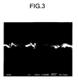
- the corrosion-resistant metallic material film 10 formed by sputtering has a large number of regular or irregular recesses 12 in the surface thereof to have irregularities at least on the surface side thereof (see FIGS. 1 and 2 schematically showing the irregularities by substantially triangular cross sections, or FIG. 3 showing an electron micrograph). If the corrosion-resistant metallic material film 10 formed by sputtering is formed at a low temperature (e.g., 25 °C) of the counter substrate member 8, the movement of atoms entering the counter substrate member 8 on the surface thereof are influenced by absorbed atoms (adatoms) to form a crystal structure which has tapered side faces and a semi-spherical dome-shaped upper end portion, so that the surface has irregularities.
- a low temperature e.g. 25 °C
- the crystal structure of the corrosion-resistant metallic material film 10 can also be controlled by parameters, such as the gas pressure in the sputtering apparatus and the input power to the sputtering apparatus, in addition to the temperature of the counter substrate member 8.
- the surface of the corrosion-resistant metallic material film 10 can be formed so as to have a desired irregular or concavoconvex shape.
- FIG. 3 is an electron micrograph showing a titanium filmservingasacorrosion-resistantmetallicmaterial film 10 which has a dome-shaped crystal structure formed on a glass plate serving as a counter substrate member 8.
- the surface of the titanium film has irregularities having a height or depth of about 10 to 100 nm.
- the irregularities of the titanium film can be formed so that the height of convexes (or protrusions) or the depth of concaves (or recesses) is preferably in the range of from about 1 nm to about 1000 nm, and more preferably in the range of from about 10 nm to about 100 nm.
- the conductive catalytic material film 11 formed on the corrosion-resistant metallic material film 10 may be made of platinum, carbon or palladium, and is preferably platinum.
- the conductive catalytic material film 11 may be formed on the corrosion-resistant metallic material film 10 by sputtering so as to have a predetermined thickness (e.g., 10 nm) (see FIGS. 1 and 2).
- a predetermined thickness e.g. 10 nm
- platinum is used as the material of the conductive catalytic material film 11
- platinum is used as a target material.
- argon gas is fed into a sputtering apparatus at 10 sccm, and the pressure in the apparatus is set to be about 1 Pa. A power of 1 kW is applied to the interior of the apparatus to produce plasma.
- the thickness of platinum is controlled in accordance with the deposition time.
- the conductive catalytic material film 11 is formed so as to have recesses 13 which correspond to the recesses 12 of the corrosion-resistant metallic material film 10.
- the counter electrode 3 is formed so as to have the irregularities of the corrosion-resistant metallic material film 10 and conductive catalytic material film 11 on the side of the electrolyte 4 (see FIGS. 1 and 2 schematically showing the irregularities by substantially triangular cross sections, or FIG. 3 showing an electron micrograph).
- FIGS. 1 and 2 schematically showing the irregularities by substantially triangular cross sections, or FIG. 3 showing an electron micrograph.
- platinic acid may be used as a raw material for casting or plating.
- the porous semiconductor electrode film 7 of the photoelectrode 2 thus formed is arranged so as to face the conductive catalytic material film 11 of the counter electrode 3 at an interval, and then, the electrolyte 4 is filled in a space between the porous semiconductor electrode film 7 and the conductive catalytic material film 11 to form the dye sensitizing solar cell 1 in this preferred embodiment (see FIG. 1).
- electrolyte 4 a redox electrolytic solution containing an oxidation-reduction pair, such as an iodine-iodine compound or abromine-bromine compound, is usuallyused.
- the electrolyte 4 may be a solid electrolyte solidified by using a gelling agent or a p-type semiconductor (CuI), in place of the above described liquid electrolyte.
- the sensitizing solar cell 1 if sunlight is incident on the photoelectrode 2 from the outside, the sensitizing dye absorbed and carried on the porous semiconductor electrode film 7 is excited to an excited state from an electronic ground state.
- the electrons of the excited sensitizing dye are injected into the conduction band of TiO 2 forming the porous semiconductor electrode film 7, to move so as to substantially take the shortest route to the transparent electrode film 6.
- the electrons moving to the transparent electrode film 6 move to the corrosion-resistant metallic material film 10 of the counter electrode 3 via an external circuit (not shown).
- the electrons moving to the corrosion-resistant metallic material film 10 move to the electrolyte 4 via the conductive catalytic material film 11 to be carried on ions in the electrolyte 4 to return to the sensitizing dye. Such an operation is repeated to extract electric energy.
- the corrosion-resistant metallic material film 10 since the corrosion-resistant metallic material film 10 is formed on the counter substrate member 8 by sputtering, the corrosion-resistant metallic material film 10 thus formed has an irregular or concavoconvex structure wherein a large number of fine recesses 12 are formed in the surface thereof. In addition, since the corrosion-resistant metallic material film 10 is continuously formed in vacuum, the surface of the corrosion-resistant metallic material film 10 is not oxidized.
- the conductive catalytic material film 11 is formed on the corrosion-resistant metallic material film 10 by sputtering, the contact area of the corrosion-resistant metallic material film 10 with the conductive catalytic material film 11 is increased, and the movement of electrons is not obstructed by the oxide film of the corrosion-resistant metallic material film 10.
- the surface of the corrosion-resistant metallic material film 10 formed on the counter substrate member 8 has the large number of fine recesses 12, and since the conductive catalytic material film 11 is formed so as to extend along the corrosion-resistant metallic material film 10, the surface of the conductive catalytic material film 11 also has the large number of fine recesses 13, and the contact area of the conductive catalytic material film 11 with the electrolyte 4 is increased. As a result, even if the thickness of the conductive catalytic material film 11 is decreased, the electric resistance of the counter electrode 3 does not increase.
- the dye sensitizing solar cell 1 in this preferred embodiment can smoothly move electrons between the counter electrode 3 and the photoelectrode 2 even if the thickness of the conductive catalytic material film 11 of the counter electrode 3 is decreased. Therefore, it is possible to enhance the photoelectric transfer efficiency of the dye sensitizing solar cell 1, and it is possible to reduce the costs for preparing parts of the counter electrode 3. In particular, according to this preferred embodiment, the costs can be greatly reduced when the material of the conductive catalytic material film 11 of the counter electrode 3 is platinum.
- the dye sensitizing solar cell 1 in this preferred embodiment is designed to cause sunlight to be incident on the substrate member 5, so that the substrate member 5 is made of a transparent plastic material having an excellent light permeability. Therefore, in this preferred embodiment, it is not always required that the counter substrate 8 is made of a plastic material having an excellent light permeability.
- the counter electrode 3 should not be limited to that in the preferred embodiment shown in FIGS. 1 and 2 according to the present invention.
- the surface (the upper surface in FIGS. 1 and 2) of the counter substrate member 8 may have a large number of recesses, and the corrosion-resistant metallic material film 10 and the conductive catalytic material film 11 may be sequentially formed on the surface of the counter substrate member 8 so that the corrosion-resistant metallic material film 10 and conductive catalytic material film 11 have an irregular or concavoconvex structure.
- a titanium film having a thickness of 300 nm serving as the corrosion-resistant metallic material film 11 was formed by sputtering while conditions were adjusted so as to obtain an irregular or concavoconvex structure by controlling the temperature of the substrate and the gas pressure (e. g. , the temperature of the substrate was 25 °C, the gas pressure was 1 Pa, and the electric energywas DC500W) .
- the gas pressure e. g. , the temperature of the substrate was 25 °C, the gas pressure was 1 Pa, and the electric energywas DC500W
- a platinum film having a thickness of 10 nm serving as the conductive catalytic material film 11 was formed by sputtering.
- the conductive film serving as the counter electrode 3 was formed.
- the surface of the conductive film had an irregular or concavoconvex structure wherein irregularities were arranged at intervals of 10 to 100 nm.
- the sheet resistance of the conductive film serving as the counter electrode 3 was 5 ⁇ / ⁇ .
- a plurality of dye sensitizing solar cells in this preferred embodiment are connected to each other in series, or if a plurality of solar cell series, each of which is formed by connecting a plurality of dye sensitizing solar cells in this preferred embodiment to each other in series, are connected to each other in parallel to form a dye sensitizing solar cell assembly, it is possible to obtain electric energy having a desired voltage value. Moreover, if the dye sensitizing solar cell assembly is connected to a storage battery, it is possible to store electric energy.
Applications Claiming Priority (1)
| Application Number | Priority Date | Filing Date | Title |
|---|---|---|---|
| JP2004333687A JP2006147261A (ja) | 2004-11-17 | 2004-11-17 | 色素増感太陽電池の対向電極及び色素増感太陽電池 |
Publications (2)
| Publication Number | Publication Date |
|---|---|
| EP1659599A2 true EP1659599A2 (fr) | 2006-05-24 |
| EP1659599A3 EP1659599A3 (fr) | 2006-07-26 |
Family
ID=35953997
Family Applications (1)
| Application Number | Title | Priority Date | Filing Date |
|---|---|---|---|
| EP05024902A Withdrawn EP1659599A3 (fr) | 2004-11-17 | 2005-11-15 | Contre électrode pour cellule photovoltaique comportant un pigment photosensible, et cellule photovoltaique comportant ledit pigment |
Country Status (3)
| Country | Link |
|---|---|
| US (1) | US20060102229A1 (fr) |
| EP (1) | EP1659599A3 (fr) |
| JP (1) | JP2006147261A (fr) |
Cited By (2)
| Publication number | Priority date | Publication date | Assignee | Title |
|---|---|---|---|---|
| EP2352202A1 (fr) * | 2008-11-26 | 2011-08-03 | Sony Corporation | Dispositif fonctionnel et son procédé de fabrication |
| AU2009303186B2 (en) * | 2008-10-10 | 2014-01-23 | Nisshin Steel Co., Ltd. | Dye-sensitized solar cells |
Families Citing this family (14)
| Publication number | Priority date | Publication date | Assignee | Title |
|---|---|---|---|---|
| JP5135744B2 (ja) * | 2006-09-20 | 2013-02-06 | 株式会社明電舎 | 色素増感太陽電池 |
| JP4488034B2 (ja) * | 2007-06-29 | 2010-06-23 | 株式会社日立製作所 | 色素増感太陽電池 |
| JP4945491B2 (ja) * | 2008-03-24 | 2012-06-06 | 株式会社Spd研究所 | 積層電極およびそれを用いた色素増感太陽電池 |
| JP5406570B2 (ja) * | 2009-03-13 | 2014-02-05 | アイシン精機株式会社 | 色素増感型太陽電池及びその製造方法 |
| WO2010119775A1 (fr) * | 2009-04-15 | 2010-10-21 | シャープ株式会社 | Cellule solaire à colorant et module de cellule solaire à colorant |
| US8372678B2 (en) * | 2009-12-21 | 2013-02-12 | Honeywell International Inc. | Counter electrode for solar cell |
| JP2011204464A (ja) * | 2010-03-25 | 2011-10-13 | Casio Computer Co Ltd | 色素増感太陽電池 |
| JP5851938B2 (ja) * | 2012-05-29 | 2016-02-03 | 株式会社Neomaxマテリアル | 色素増感型太陽電池用金属基板 |
| CN103515104B (zh) * | 2012-06-21 | 2017-09-26 | 日立金属株式会社 | 色素增感型太阳能电池用金属基板 |
| US10121602B2 (en) * | 2012-06-22 | 2018-11-06 | Hitachi Metals, Ltd. | Metal substrate for dye-sensitized solar cell |
| JP5382186B1 (ja) * | 2012-10-10 | 2014-01-08 | ウシオ電機株式会社 | 色素増感型太陽電池 |
| JP2014238969A (ja) * | 2013-06-07 | 2014-12-18 | シャープ株式会社 | 太陽電池 |
| US10605760B2 (en) | 2014-07-22 | 2020-03-31 | Toyobo Co., Ltd. | Thin film-laminated film |
| CN113345968B (zh) * | 2021-05-31 | 2022-07-12 | 武汉华星光电技术有限公司 | 薄膜晶体管、薄膜晶体管的制作方法和显示面板 |
Citations (1)
| Publication number | Priority date | Publication date | Assignee | Title |
|---|---|---|---|---|
| WO2004006381A1 (fr) * | 2002-07-09 | 2004-01-15 | Fujikura Ltd. | Cellule solaire |
Family Cites Families (6)
| Publication number | Priority date | Publication date | Assignee | Title |
|---|---|---|---|---|
| AU774443B2 (en) * | 1999-06-30 | 2004-06-24 | Jgc Catalysts And Chemicals Ltd. | Photoelectric cell |
| US7022910B2 (en) * | 2002-03-29 | 2006-04-04 | Konarka Technologies, Inc. | Photovoltaic cells utilizing mesh electrodes |
| JP4213355B2 (ja) * | 2001-02-28 | 2009-01-21 | 株式会社豊田中央研究所 | 色素増感型太陽電池及び色素増感型太陽電池モジュール |
| JP4037618B2 (ja) * | 2001-04-13 | 2008-01-23 | アイシン精機株式会社 | 色素増感型太陽電池及びその製造方法 |
| JP4894101B2 (ja) * | 2001-07-19 | 2012-03-14 | アイシン精機株式会社 | 色素増感型太陽電池の対極の製造方法、色素増感型太陽電池の製造方法 |
| US7145071B2 (en) * | 2002-12-11 | 2006-12-05 | General Electric Company | Dye sensitized solar cell having finger electrodes |
-
2004
- 2004-11-17 JP JP2004333687A patent/JP2006147261A/ja active Pending
-
2005
- 2005-11-14 US US11/274,082 patent/US20060102229A1/en not_active Abandoned
- 2005-11-15 EP EP05024902A patent/EP1659599A3/fr not_active Withdrawn
Patent Citations (1)
| Publication number | Priority date | Publication date | Assignee | Title |
|---|---|---|---|---|
| WO2004006381A1 (fr) * | 2002-07-09 | 2004-01-15 | Fujikura Ltd. | Cellule solaire |
Non-Patent Citations (2)
| Title |
|---|
| CAMERON P J ET AL: "Electrochemical studies of the Co(III)/Co(II)(dbbip)2 redox couple as a mediator for dye-sensitized nanocrystalline solar cells" COORDINATION CHEMISTRY REVIEWS, ELSEVIER SCIENCE, AMSTERDAM, NL, vol. 248, no. 13-14, July 2004 (2004-07), pages 1447-1453, XP004578930 ISSN: 0010-8545 * |
| HAUCH A ET AL: "Diffusion in the electrolyte and charge-transfer reaction at the platinum electrode in dye-sensitized solar cells" ELECTROCHIMICA ACTA, ELSEVIER SCIENCE PUBLISHERS, BARKING, GB, vol. 46, no. 22, 1 August 2001 (2001-08-01), pages 3457-3466, XP004298164 ISSN: 0013-4686 * |
Cited By (4)
| Publication number | Priority date | Publication date | Assignee | Title |
|---|---|---|---|---|
| AU2009303186B2 (en) * | 2008-10-10 | 2014-01-23 | Nisshin Steel Co., Ltd. | Dye-sensitized solar cells |
| EP2352202A1 (fr) * | 2008-11-26 | 2011-08-03 | Sony Corporation | Dispositif fonctionnel et son procédé de fabrication |
| EP2352202A4 (fr) * | 2008-11-26 | 2012-05-23 | Sony Corp | Dispositif fonctionnel et son procédé de fabrication |
| EP2458605A1 (fr) | 2008-11-26 | 2012-05-30 | Sony Corporation | Dispositif fonctionnel et son procédé de production |
Also Published As
| Publication number | Publication date |
|---|---|
| JP2006147261A (ja) | 2006-06-08 |
| US20060102229A1 (en) | 2006-05-18 |
| EP1659599A3 (fr) | 2006-07-26 |
Similar Documents
| Publication | Publication Date | Title |
|---|---|---|
| EP1659599A2 (fr) | Contre électrode pour cellule photovoltaique comportant un pigment photosensible, et cellule photovoltaique comportant ledit pigment | |
| EP1643516A1 (fr) | Photoélectrode pour cellule solaire avec colorant sensibilisateur ou cellule solaire organique | |
| US8637766B2 (en) | Dye-sensitized solar cell | |
| JP2001093591A (ja) | 光電変換素子 | |
| US20090078307A1 (en) | Three-Pole Two-Layer Photo-Rechargeable Battery | |
| EP1646059A3 (fr) | Contre-électrode très efficace pour une cellule solaire sensibilisée par un colorant et méthode de production | |
| JP2007134328A (ja) | 太陽電池及びその製造方法 | |
| JP5458271B2 (ja) | 色素増感太陽電池およびその製造方法 | |
| US20130237006A1 (en) | Dye-sensitized solar cell and method of fabricating the same | |
| US7858213B2 (en) | Hybrid electrode and method of preparing the same | |
| JP2000285974A (ja) | 光増感型太陽光発電素子 | |
| EP1753000A2 (fr) | Substrat de photoelectrode d'une cellule solaire avec colorant sensibilisateur et méthode pour sa fabrication | |
| JP2007294288A (ja) | 色素増感型太陽電池 | |
| JP5699828B2 (ja) | 色素増感太陽電池用アノードの製造方法 | |
| JP5095126B2 (ja) | 光電変換素子 | |
| KR101583701B1 (ko) | 수퍼캐패시터용 투명전극, 그 제조방법 및 상기 투명전극을 포함한 수퍼캐패시터 | |
| JP4872861B2 (ja) | プラズモン共鳴型光電変換素子および該製造方法 | |
| JP2007115514A (ja) | 色素増感太陽電池の作用極及びそれを備えた色素増感太陽電池並びに色素増感太陽電池の作用極の製造方法 | |
| JP5148835B2 (ja) | 色素増感型太陽電池およびその光電極基板 | |
| JP2007257930A (ja) | 色素増感型太陽電池 | |
| JP2005317225A (ja) | 色素増感型太陽電池、及び色素増感型太陽電池の光電極基板 | |
| JP4061811B2 (ja) | 半導体電極、半導体電極の製造方法および太陽電池 | |
| JP5048281B2 (ja) | 色素増感太陽電池およびその製造方法 | |
| JP5128076B2 (ja) | 色素増感型太陽電池及びその製造方法 | |
| JP5025938B2 (ja) | 色素増感型太陽電池、その対向電極およびその対向電極の製造方法 |
Legal Events
| Date | Code | Title | Description |
|---|---|---|---|
| PUAI | Public reference made under article 153(3) epc to a published international application that has entered the european phase |
Free format text: ORIGINAL CODE: 0009012 |
|
| AK | Designated contracting states |
Kind code of ref document: A2 Designated state(s): AT BE BG CH CY CZ DE DK EE ES FI FR GB GR HU IE IS IT LI LT LU LV MC NL PL PT RO SE SI SK TR |
|
| AX | Request for extension of the european patent |
Extension state: AL BA HR MK YU |
|
| PUAL | Search report despatched |
Free format text: ORIGINAL CODE: 0009013 |
|
| AK | Designated contracting states |
Kind code of ref document: A3 Designated state(s): AT BE BG CH CY CZ DE DK EE ES FI FR GB GR HU IE IS IT LI LT LU LV MC NL PL PT RO SE SI SK TR |
|
| AX | Request for extension of the european patent |
Extension state: AL BA HR MK YU |
|
| 17P | Request for examination filed |
Effective date: 20061030 |
|
| AKX | Designation fees paid |
Designated state(s): AT BE BG CH CY CZ DE DK EE ES FI FR GB GR HU IE IS IT LI LT LU LV MC NL PL PT RO SE SI SK TR |
|
| STAA | Information on the status of an ep patent application or granted ep patent |
Free format text: STATUS: THE APPLICATION IS DEEMED TO BE WITHDRAWN |
|
| 18D | Application deemed to be withdrawn |
Effective date: 20110601 |